JP2005292234A - Liquid crystal panel and liquid crystal display using the same - Google Patents
Liquid crystal panel and liquid crystal display using the same Download PDFInfo
- Publication number
- JP2005292234A JP2005292234A JP2004103611A JP2004103611A JP2005292234A JP 2005292234 A JP2005292234 A JP 2005292234A JP 2004103611 A JP2004103611 A JP 2004103611A JP 2004103611 A JP2004103611 A JP 2004103611A JP 2005292234 A JP2005292234 A JP 2005292234A
- Authority
- JP
- Japan
- Prior art keywords
- liquid crystal
- substrate
- alignment
- phase
- crystal panel
- Prior art date
- Legal status (The legal status is an assumption and is not a legal conclusion. Google has not performed a legal analysis and makes no representation as to the accuracy of the status listed.)
- Granted
Links
Images


Abstract
Description
本発明は、液晶TVまたはパソコン用液晶モニタ等に用いることのできる、液晶パネル、液晶表示装置に関し、特にアクティブマトリックス駆動型の液晶表示装置に好適に用いることのできる、強誘電性液晶を用いた液晶パネル、液晶表示装置に関する。 The present invention relates to a liquid crystal panel and a liquid crystal display device that can be used for a liquid crystal TV or a liquid crystal monitor for a personal computer, and in particular, a ferroelectric liquid crystal that can be suitably used for an active matrix drive type liquid crystal display device is used. The present invention relates to a liquid crystal panel and a liquid crystal display device.
近年、フラットディスプレイとして、液晶表示装置の市場が急拡大している。液晶表示装置には、互いに直交するストライプ状の電極で液晶を駆動する単純マトリックス駆動型と、薄膜トランジスタ(TFT)素子等によるアクティブマトリックス駆動型とに大別されるが、近年、アクティブマトリックス駆動型の液晶表示装置のコストダウンと大画面化が進展し、液晶TV用途等の動画表示の利用に供されている。 In recent years, the market for liquid crystal display devices as a flat display has been rapidly expanding. Liquid crystal display devices are roughly classified into a simple matrix driving type in which liquid crystal is driven by stripe electrodes orthogonal to each other and an active matrix driving type using a thin film transistor (TFT) element. Liquid crystal display devices are being reduced in cost and increased in screen size, and are being used for video display applications such as liquid crystal TV applications.
このように液晶表示装置は、動画表示に利用されているが、従来使用されているネマチック液晶は、電圧印加に対する応答が遅いために、特に液晶表示装置を大画面化した際に、動画表示の速い動きに追随することができないため画質が低下するという問題があり、この問題の解決が課題となっている。 As described above, the liquid crystal display device is used for moving image display. However, the nematic liquid crystal that has been used in the past has a slow response to voltage application. There is a problem that the image quality deteriorates because it cannot follow the fast movement, and the solution to this problem is an issue.
こうした中、ネマチック液晶と比較して応答が速い強誘電性液晶を液晶表示装置へ適用することが検討されている。 Under such circumstances, it has been studied to apply a ferroelectric liquid crystal having a quick response compared with a nematic liquid crystal to a liquid crystal display device.
特開昭56−107216号公報には、双安定性を有する強誘電性液晶のメモリー性を利用した液晶表示装置が開示されている。しかしながら、このように双安定強誘電性液晶は、電圧−光透過率曲線(VT曲線)にヒステリシスを有するので、TFT素子等によるアクティブマトリックス駆動法の適用が困難であることから、主に単純マトリックス駆動型の液晶表示装置への適用が検討されてきた。 Japanese Patent Application Laid-Open No. 56-107216 discloses a liquid crystal display device using the memory property of ferroelectric liquid crystal having bistability. However, since the bistable ferroelectric liquid crystal has hysteresis in the voltage-light transmittance curve (VT curve) as described above, it is difficult to apply the active matrix driving method using a TFT element or the like. Application to drive-type liquid crystal display devices has been studied.
しかし、近年、電圧無印加時に単安定分子配向を有する強誘電性液晶を用いて前記VT曲線のヒステリシスを解消することで、アクティブマトリックス駆動に適した強誘電性液晶表示装置を実現することが提案されている((1)特許第2921577号公報、(2)特許第3403114号公報、(3)特開2003−5223号公報、(4)特許第3466635号公報)。特に特許文献(2)および特許文献(3)には、相転移系列として、等方液体相−コレステリック相−カイラルスメクチックC相、または、等方液体相−カイラルスメクチックC相を示す強誘電性液晶に着目し、電界を印加しながら強誘電性液晶相に徐冷すること(以下、電界印加徐冷という。)によって、ヒステリシスのないV字状またはハーフV字状のVT曲線が得られることが開示されており、また、特許文献(2)には液晶性光反応性モノマーを強誘電性液晶に混合し、強誘電性液晶の高温相で液晶層に電界印加と紫外線照射を行ない室温まで徐冷する方法(以下、高分子安定化法という。)等によっても、ヒステリシスのないV字状またはハーフV字状のVT曲線が得られることが開示されている。 However, in recent years, it has been proposed to realize a ferroelectric liquid crystal display device suitable for active matrix driving by eliminating the hysteresis of the VT curve using a ferroelectric liquid crystal having monostable molecular orientation when no voltage is applied. ((1) Japanese Patent No. 2921577, (2) Japanese Patent No. 3403114, (3) Japanese Patent Laid-Open No. 2003-5223, (4) Japanese Patent No. 3466635). In particular, in Patent Document (2) and Patent Document (3), a ferroelectric liquid crystal showing an isotropic liquid phase-cholesteric phase-chiral smectic C phase or an isotropic liquid phase-chiral smectic C phase as a phase transition series. Focusing on the above, by slowly cooling the ferroelectric liquid crystal phase while applying an electric field (hereinafter referred to as electric field applied gradual cooling), a V-shaped or half V-shaped VT curve without hysteresis can be obtained. Patent Document (2) discloses that a liquid crystalline photoreactive monomer is mixed with a ferroelectric liquid crystal, an electric field is applied to the liquid crystal layer in the high temperature phase of the ferroelectric liquid crystal and ultraviolet irradiation is performed, and the temperature is gradually lowered to room temperature. It is disclosed that a V-shaped or half V-shaped VT curve having no hysteresis can be obtained by a cooling method (hereinafter referred to as a polymer stabilization method) or the like.
また、特許文献(4)には、相転移系列にスメクチックA相を有する強誘電性液晶を用いても、所定の電界を印加して徐冷することにより単安定分子配向した強誘電性液晶が得られることが開示してあり、当該強誘電性液晶と三原色の各光を継続的に切り替え照射させるバックライトの構成により、アナログ階調が可能な高速応答性に優れたフルカラー表示が得られることが開示されている。
しかしながら、上記電界印加徐冷法においては、コレステリック相からカイラルスメクチックC相(強誘電性液晶相)へ相転移する際に、液晶表示装置の各画素に電圧を印加するという余分のプロセスが必要であり、コストアップの要因となる。さらに、上記高分子安定化法においても、コレステリック相またはスメクチックA相からカイラルスメクチックC相(強誘電性液晶)へ相転移する際に、液晶表示装置の各画素に電圧を印加しながら紫外光を照射するという複雑なプロセスが必要であり、コストアップの要因となる。 However, the electric field application slow cooling method requires an extra process of applying a voltage to each pixel of the liquid crystal display device when the cholesteric phase transitions to the chiral smectic C phase (ferroelectric liquid crystal phase). This will increase costs. Further, in the above polymer stabilization method, ultraviolet light is applied while applying a voltage to each pixel of the liquid crystal display device when the phase transition from the cholesteric phase or smectic A phase to the chiral smectic C phase (ferroelectric liquid crystal). A complicated process of irradiation is necessary, which increases costs.
本発明は、このような課題を解決するするためになされたものであって、その目的は、コスト上昇要因である上述の電界印加処理や紫外線照射のプロセスを不要としつつ、TFT素子等によるアクティブマトリックス駆動に適した液晶パネルを提供し、さらには、高品質で高速なフルカラー動画表示を実現できる液晶表示装置を提供することにある。 The present invention has been made to solve such problems, and its purpose is to eliminate the need for the above-described electric field application process and ultraviolet irradiation process, which are cost-increased factors. An object of the present invention is to provide a liquid crystal panel suitable for matrix driving, and further to provide a liquid crystal display device capable of realizing high-quality and high-speed full-color moving image display.
本発明者は、各種相転移系列を有する強誘電性液晶を用いて、液晶パネルにおける各種配向膜材料および配向処理方法を検討した。その結果、一方の基板は一方向への配向処理が施され、他方の基板は、異なる方向に配向処理が施された単一または複数の領域を有するものとすることによって、前記電界印加徐冷および前記紫外線照射のプロセスを使用することなく、ヒステリシスのないVT曲線を得ることができ、前記強誘電性液晶を用いた液晶表示装置をTFT素子等によるアクティブマトリックス駆動できることを見出した。 The present inventor has studied various alignment film materials and alignment treatment methods in liquid crystal panels using ferroelectric liquid crystals having various phase transition series. As a result, one substrate is subjected to orientation treatment in one direction, and the other substrate has single or plural regions subjected to orientation treatment in different directions. It has also been found that a VT curve without hysteresis can be obtained without using the ultraviolet irradiation process, and that the liquid crystal display device using the ferroelectric liquid crystal can be driven in an active matrix by a TFT element or the like.
上記課題を解決するための本発明の液晶表示装置は、上記知見に基づいてなされたものである。 The liquid crystal display device of the present invention for solving the above problems has been made based on the above findings.
即ち、本発明に係る液晶パネルは、一対の基板間に、相転移系列として、等方液体相−コレステリック相−カイラルスメクチックC相を有する液晶が封入されてなる液晶パネルであって、前記基板のうち、第1の基板は配向処理が施され、第2の基板は少なくともその一部が、第1の基板に施された配向処理方向と異なる方向に配向処理が施され、電圧無印加時に前記カイラルスメクチックC相において、前記液晶が一様な単安定分子配向を有していることを特徴とするものである。 That is, the liquid crystal panel according to the present invention is a liquid crystal panel in which a liquid crystal having an isotropic liquid phase-cholesteric phase-chiral smectic C phase as a phase transition series is sealed between a pair of substrates. Among them, the first substrate is subjected to an alignment treatment, and at least a part of the second substrate is subjected to an alignment treatment in a direction different from the alignment treatment direction applied to the first substrate. In the chiral smectic C phase, the liquid crystal has a uniform monostable molecular orientation.
また、本発明に係る液晶パネルでは、前記第2の基板は、前記第1の基板に施した配向処理方向と異なる方向に単一の配向処理が施されていてもよいが、隣接する領域が相互に異なる方向に配向処理が施されてなる複数の配向処理領域を有していてもよい。 In the liquid crystal panel according to the present invention, the second substrate may be subjected to a single alignment process in a direction different from the alignment process direction applied to the first substrate. You may have the some orientation processing area | region by which orientation processing is performed in a mutually different direction.
さらに、本発明に係る液晶パネルでは、好ましくは前記コレステリック相において、当該液晶の分子配向が、前記第1の基板から前記第2の基板に向かってツイストしていることができ、特に好ましくは前記複数の配向領域を有する場合には、前記コレステリック相において、前記液晶が前記複数の配向処理領域で配向分割されていることができる。 Furthermore, in the liquid crystal panel according to the present invention, preferably in the cholesteric phase, the molecular orientation of the liquid crystal can be twisted from the first substrate toward the second substrate, and particularly preferably In the case of having a plurality of alignment regions, in the cholesteric phase, the liquid crystal can be divided in the plurality of alignment treatment regions.
なお、本発明においては、第1の基板の配向膜と、第2の基板の配向膜とが、表面をラビング配向処理または偏光紫外光照射による配向処理が施されたポリイミド配向膜であっても良く、第1の基板の配向膜と、第2の基板の配向膜とが、表面に紫外光照射による配向処理が施された光配向膜であっても良い。さらに、第1の基板の配向膜がポリイミド配向膜であり、第2の基板の配向膜が光配向膜であっても良い。さらに、本発明においては、前記第2の基板の方位角アンカリングエネルギーが、前記第1の基板の方位角アンカリングエネルギーよりも小さいことが好ましい。 In the present invention, the alignment film of the first substrate and the alignment film of the second substrate may be polyimide alignment films whose surfaces have been subjected to a rubbing alignment process or an alignment process by irradiation with polarized ultraviolet light. Alternatively, the alignment film of the first substrate and the alignment film of the second substrate may be a photo-alignment film whose surface is subjected to an alignment process by irradiation with ultraviolet light. Furthermore, the alignment film of the first substrate may be a polyimide alignment film, and the alignment film of the second substrate may be a photo-alignment film. Furthermore, in the present invention, it is preferable that the azimuth anchoring energy of the second substrate is smaller than the azimuth anchoring energy of the first substrate.
また、本発明に係る液晶パネルは、前記第1基板または前記第2基板に、各画素に対応してアクティブマトリックス駆動を行うための薄膜トランジスタを有することを特徴とする。 The liquid crystal panel according to the present invention includes a thin film transistor for performing active matrix driving corresponding to each pixel on the first substrate or the second substrate.
なお、本発明に係る液晶表示装置は、好ましくは前記第1基板または前記第2基板に、各画素に対応してアクティブマトリックス駆動を行うための薄膜トランジスタを有する液晶パネルと、複数色のLEDからなるバックライトと、前記薄膜トランジスタに電圧を供給して前記液晶をスイッチングさせるための駆動回路を有し、さらに、好ましくは前記液晶のスイッチングに同期して、前記LEDを色順次に点灯することによりカラー表示を行う液晶表示装置であることができる。 The liquid crystal display device according to the present invention preferably includes a liquid crystal panel having thin film transistors for performing active matrix driving corresponding to each pixel on the first substrate or the second substrate, and a plurality of LEDs. A backlight and a driving circuit for switching the liquid crystal by supplying a voltage to the thin film transistor, and further preferably performing color display by lighting the LEDs in color sequence in synchronization with the switching of the liquid crystal It can be a liquid crystal display device.
また、好ましくは前記第1の基板または第2の基板に、カラーフィルタを有し、前記カラーフィルタを有する基板とは異なる基板に、前記薄膜トランジスタを有していても良いが、前記第1の基板または前記第2の基板に、薄膜トランジスタと、当該薄膜トランジスタ上に複数色の着色層からなるオンアレイタイプのカラーフィルタを有していても良い。 Preferably, the first substrate or the second substrate has a color filter, and the thin film transistor may be included in a substrate different from the substrate having the color filter. Alternatively, the second substrate may include a thin film transistor and an on-array type color filter including a plurality of colored layers on the thin film transistor.
本発明に係る液晶表示装置の他の構成は、好ましくは前記カラーフィルタまたはオンアレイタイプのカラーフィルタおよび前記薄膜トランジスタを有する、前記液晶パネルと、複数の冷陰極管または白色LEDからなるバックライトと、前記薄膜トランジスタに電圧を供給して前記液晶をスイッチングさせる駆動回路を有することができる。 Another configuration of the liquid crystal display device according to the present invention is preferably the liquid crystal panel having the color filter or the on-array type color filter and the thin film transistor, and a backlight composed of a plurality of cold cathode tubes or white LEDs, A driving circuit for supplying a voltage to the thin film transistor to switch the liquid crystal may be provided.
本発明によれば、前記カイラルスメクチックC相(強誘電性液晶相)において単安定分子配向が得られ、且つ、ヒステリシスのないVT曲線が得られるので、TFT素子等によるアクティブマトリックス駆動による階調表示が可能となる。また特に、コスト上昇要因である液晶層に対する電界印加処理や紫外線照射等のプロセスが不要となるので、高品質かつ高速で動画表示可能なアクティブマトリックス駆動に適した液晶パネル、液晶表示装置の提供を低コストで実現できる。 According to the present invention, a monostable molecular orientation is obtained in the chiral smectic C phase (ferroelectric liquid crystal phase), and a VT curve without hysteresis is obtained, so that gradation display by active matrix driving by a TFT element or the like is obtained. Is possible. In particular, it eliminates the need for electric field application processing and ultraviolet irradiation, etc., on the liquid crystal layer, which is a cause of increased costs, and therefore provides liquid crystal panels and liquid crystal display devices suitable for active matrix driving capable of displaying moving images at high speed and high speed. Realized at low cost.
以下、本発明の液晶パネル、液晶表示装置について、図面を参照して説明する。 Hereinafter, a liquid crystal panel and a liquid crystal display device of the present invention will be described with reference to the drawings.
(液晶パネル、液晶表示装置)
図1は本発明に係る液晶パネルの一例を示す概略断面図である。この液晶パネル1は、共通電極112および配向膜113が形成された第1の基板115と、TFT素子121、画素電極122、および配向膜123が形成された第2の基板125とを所定の間隔で対向させた間隙に強誘電性液晶層131が形成され、第1の基板と第2の基板とを、所定の間隔で対向させるために、基板間に、ガラスまたは樹脂からなるスペーサ132が配置されている。さらに、基板115上には、液晶層131に並列に保持容量が形成されているのが好ましい(図示せず)。保持容量は、自発分極の大きさにも依存するが、自発分極が2〜10nC/cm2の大きさの範囲にあるとき、各画素の液晶層に対応した静電容量の1倍〜10倍程度の大きさが好ましい。
(Liquid crystal panel, liquid crystal display device)
FIG. 1 is a schematic sectional view showing an example of a liquid crystal panel according to the present invention. In the
なお、図1の、前記配向膜113には、一方向に配向処理が施されており、前記配向膜123は、配向膜113に施した配向方向とは異なる方向に配向処理が施された単一または複数の領域を有している。
In FIG. 1, the
図2は本発明に係る液晶パネルの他の例を示す概略断面図である。この液晶パネル2は、カラーフィルタ211、共通電極212および配向膜213が形成された第1の基板215と、TFT素子221、画素電極222、配向膜223が形成された第2の基板225とを所定の間隔で対向させた間隙に強誘電性液晶層231が形成され、第1の基板と第2の基板とを、所定の間隔で対向させるために、基板間に、ガラスまたは樹脂からなるスペーサ232が配置されている。さらに、基板215上には、液晶層231に並列に保持容量が形成されているのが好ましい(図示せず)。保持容量は、自発分極の大きさにも依存するが、自発分極が2〜10nC/cm2の大きさの範囲にあるとき、各画素の液晶層に対応した静電容量の1倍〜10倍程度の大きさが好ましい。
FIG. 2 is a schematic sectional view showing another example of the liquid crystal panel according to the present invention. The
なお、図2の、前記配向膜213には、一方向に配向処理が施されており、前記配向膜223は、配向膜213に施した配向方向とは異なる方向に配向処理が施された単一または複数の領域を有している。
Note that the
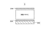
図3は本発明に係る液晶表示装置の一例を示す概略断面図である。この液晶表示装置は、図1に示した液晶パネル1、前記液晶パネル1の上面に形成された偏光板314、該液晶パネル1の下面に形成され、偏光板314と偏光軸が直交する偏光板324、およびR、G、Bの3原色等のLEDバックライト342から構成されてなる液晶表示装置である。なお、本液晶表示装置には、液晶表示を行うための駆動回路が具備されている(図示せず)。
FIG. 3 is a schematic sectional view showing an example of the liquid crystal display device according to the present invention. This liquid crystal display device includes the
図3に示した本発明に係る液晶表示装置においては、フィールドシーケンシャルカラー駆動法によるカラー液晶表示を好適に実現できる。このフィールドシーケンシャルカラー駆動法によるカラー液晶表示は、前記R、G、Bの3原色等のLEDのバックライト等を前記強誘電性液晶のスイッチングに同期して、色順次に点灯することにより達成することができる。 In the liquid crystal display device according to the present invention shown in FIG. 3, a color liquid crystal display by a field sequential color driving method can be suitably realized. The color liquid crystal display by the field sequential color driving method is achieved by lighting the backlights of the LEDs of the three primary colors such as R, G, and B in order of color in synchronization with the switching of the ferroelectric liquid crystal. be able to.
なお、例えば、テレビ表示の映像信号の方式であるNTSC(National Television Standards Committee)方式では、垂直走査周波数が60Hzとなるので、1画面の表示時間は約16.7msである。一方、前記フィールドシーケンシャルカラー駆動法では、1フィールド期間内でR,G.BのLED等のバックライトを色順次に点灯させるために、垂直走査周波数は180Hzとなり、1画面の表示時間は約5.56msと短くなる。したがって、ネマチック液晶の応答時間は数m秒乃至数十m秒と遅いことから、ネマチック液晶を用いた液晶表示装置では、前記フィールドシーケンシャルカラー駆動法で画像表示を行おうとすると、前記垂直走査周波数(180Hz)の駆動波形に追随することができずに、高品質な動画表示を行うことが困難となる。これに対して、強誘電性液晶の応答時間は1m秒以下と高速であるため、図3の本発明に係る液晶表示装置においては、前記垂直走査周波数180Hzの駆動波形に十分追随することができ、しかもヒステリシスのないVT曲線が得られるので、フィールドシーケンシャルカラー駆動法を用いて、前記アクティブマトリックス駆動により、高品質かつ高速な動画表示が可能となる。 For example, in the NTSC (National Television Standards Committee) system, which is a video signal system for television display, the vertical scanning frequency is 60 Hz, so the display time for one screen is about 16.7 ms. On the other hand, in the field sequential color driving method, R, G. In order to turn on the backlight such as the LED of B in order of color, the vertical scanning frequency is 180 Hz, and the display time of one screen is shortened to about 5.56 ms. Accordingly, since the response time of nematic liquid crystal is as slow as several milliseconds to several tens of milliseconds, in a liquid crystal display device using nematic liquid crystal, if an image is displayed by the field sequential color driving method, the vertical scanning frequency ( It is difficult to follow a drive waveform of 180 Hz), and it becomes difficult to display a high-quality moving image. On the other hand, since the response time of the ferroelectric liquid crystal is as fast as 1 ms or less, the liquid crystal display device according to the present invention shown in FIG. 3 can sufficiently follow the drive waveform at the vertical scanning frequency of 180 Hz. In addition, since a VT curve having no hysteresis is obtained, high-quality and high-speed moving image display can be performed by the active matrix driving using the field sequential color driving method.
このフィールドシーケンシャルカラー駆動法によると、カラーフィルタが不要となるので、前記カラーフィルタによる光吸収がなく、明るい表示が得られ、バックライトの消費電力も少なくて済む。また、前記フィールドシーケンシャル駆動法によるカラー表示は、画素をR,G,B3原色等のカラーフィルタ毎に空間的に分割する必要がないため、開口率が高く高精細なカラー液晶表示が可能となるというメリットがある。 According to this field sequential color driving method, since a color filter is not required, light is not absorbed by the color filter, a bright display can be obtained, and power consumption of the backlight can be reduced. Further, in the color display by the field sequential driving method, it is not necessary to spatially divide the pixels for each color filter such as R, G, B3 primary colors, so that a high-definition color liquid crystal display with a high aperture ratio becomes possible. There is a merit.
ただし、フィールドシーケンシャル駆動法を用いた液晶表示装置は、上述したメリットを有するのではあるが、例えば対角20インチ以上の大画面液晶表示装置に対しては、バックライトに使用するLEDの数量が面積に概略比例して増加するために、このような大型の液晶表示装置においては、輝度およびコスト等で制約があるため、カラーフィルタを用いた方式が有利となり得る。 However, although the liquid crystal display device using the field sequential driving method has the above-mentioned advantages, for example, for a large-screen liquid crystal display device having a diagonal of 20 inches or more, the number of LEDs used for the backlight is small. Since it increases in proportion to the area, in such a large-sized liquid crystal display device, there is a limitation in brightness, cost, etc., and therefore a method using a color filter can be advantageous.
上述したように、本発明に係る液晶表示装置は、前記強誘電性液晶の高速応答性を有効に活用できるフィールドシーケンシャルカラー駆動法による画像表示おいて最も大きな効果が得られるが、図4に示した本発明に係る液晶表示装置によれば、カラーフィルタ方式によるアクティブマトリックス駆動法を用いたカラー液晶表示に際しても、従来のネマチック液晶を用いた液晶表示装置よりも、動画像の表示品質の優れたカラー液晶表示を実現できる。 As described above, the liquid crystal display device according to the present invention is most effective in displaying an image by the field sequential color driving method capable of effectively utilizing the high-speed response of the ferroelectric liquid crystal. According to the liquid crystal display device according to the present invention, in the color liquid crystal display using the active matrix driving method by the color filter method, the moving image display quality is superior to the liquid crystal display device using the conventional nematic liquid crystal. Color liquid crystal display can be realized.
すなわち、図4は本発明に係る液晶表示装置の他の例を示す概略断面図である。この液晶表示装置は、図2に示した液晶パネル2、該液晶パネル2の上面に形成された偏光板414、該液晶パネル2の下面に形成され、偏光板414と偏光軸が直交する偏光板424、および冷陰極管または白色LED等のバックライト442から構成されてなる液晶表示装置である。なお、本液晶表示装置には、液晶表示を行うための駆動回路が具備されている(図示せず)。図4に示す強誘電性液晶パネル2では(図2参照)、カラーフィルタを有する基板とは異なる基板上に、薄膜トランジスタを有するが、その他にも、カラーフィルタと薄膜トランジスタとが同一の基板上に形成されていてもよい。
That is, FIG. 4 is a schematic sectional view showing another example of the liquid crystal display device according to the present invention. This liquid crystal display device includes the
上述したように、前記垂直走査周波数60Hzの場合であっても、図4の本発明に係る液晶表示装置は、ヒステリシスのないVT曲線を有するので、前記アクティブマトリックス駆動法を用いることができ、従来のネマチック液晶を用いた液晶表示装置よりも、高品質かつ高速な動画表示が可能である。 As described above, even in the case of the vertical scanning frequency of 60 Hz, the liquid crystal display device according to the present invention of FIG. 4 has a VT curve without hysteresis, so that the active matrix driving method can be used. High-quality and high-speed moving image display is possible as compared with a liquid crystal display device using nematic liquid crystal.
なお、これらの発明においては、2枚の基板間に設けられるスペーサの形成方法としては、球状のスペーサを予め基板上に散布により配置してもよく、あるいはフォトリソ工程で、柱状突起物あるいは壁状構造物を基板上に設けてもよい。 In these inventions, as a method for forming a spacer provided between two substrates, spherical spacers may be arranged in advance on the substrate, or a columnar projection or a wall-like shape may be formed by a photolithography process. The structure may be provided on the substrate.
(液晶配列)
前記強誘電性液晶は、自発分極を有するという特質を有する。したがって、従来のネマチック液晶は、自発分極を持たないため、駆動回路から供給される電界がネマチッック液晶の誘電率の異方部分に作用することで応答するのに対して、強誘電性液晶は自発分極に直接作用するため、ネマチック液晶の数百倍程度の大きなトルクが液晶分子に加わり、その結果、1ms以下で高速に応答することができる。特に、パネルギャップが小さい場合には、基板界面の配向規制力によって、一様に配向した表面安定化強誘電性液晶が実現し、かかる場合には前記強誘電性液晶が双安定分子配列を示すことがクラーク等により見いだされている(特開昭56−107216号公報)。図5Aと図5Bには、前記表面安定化強誘電性液晶の分子配列の概略図を示してある。図5に示すように、強誘電性液晶分子551Aおよび551Bは、基板(515A、525A、515B、525B)に平行配向し、自発分極561Aおよび561Bは基板に対して上向きまたは下向きの双安定配置をとる。スメクチック層界面541A、およびスメクチック層界面541Bが同一方向に形成される。駆動回路(図示せず)から駆動電圧を加えることによって、その電圧の極性に応じて自発分極の向きが上向きまたは下向きに反転し、電圧切断後はそのままの配列を維持するというメモリー性を有する。
(Liquid crystal alignment)
The ferroelectric liquid crystal has a characteristic of having spontaneous polarization. Therefore, the conventional nematic liquid crystal does not have spontaneous polarization, so that the electric field supplied from the drive circuit responds by acting on the anisotropic part of the dielectric constant of the nematic liquid crystal, whereas the ferroelectric liquid crystal is spontaneous. Since it acts directly on the polarization, a large torque of several hundred times that of nematic liquid crystal is applied to the liquid crystal molecules, and as a result, it can respond quickly in 1 ms or less. In particular, when the panel gap is small, a uniformly stabilized surface-stabilized ferroelectric liquid crystal is realized by the alignment regulating force at the substrate interface. In such a case, the ferroelectric liquid crystal exhibits a bistable molecular arrangement. This has been found by Clark et al. (Japanese Patent Laid-Open No. 56-107216). 5A and 5B are schematic views showing the molecular arrangement of the surface-stabilized ferroelectric liquid crystal. As shown in FIG. 5, the ferroelectric
なお、図5Aと図5Bの前記基板には通常ポリイミド樹脂等の配向膜(図示せず)が形成されており、前記配向膜の表面は一方向にラビング処理等が施されている。 5A and 5B is usually formed with an alignment film (not shown) such as polyimide resin, and the surface of the alignment film is rubbed in one direction.
図6には表面安定化強誘電性液晶のVT曲線の概略図を示す。前記表面安定化強誘電性液晶はメモリー性を有するので、VT曲線はヒステリシスを有し、電圧無印加時(V=0)に明と暗の2状態をとる。このため、表面安定化強誘電性液晶は、従来、主に単純マトリックス駆動方式による液晶表示装置に使用されており、階調表示が困難なため、TFT素子等によるアクティブマトリックス駆動法の適用がむずかしいと考えられていた。 FIG. 6 shows a schematic diagram of the VT curve of the surface-stabilized ferroelectric liquid crystal. Since the surface-stabilized ferroelectric liquid crystal has a memory property, the VT curve has hysteresis and takes two states of light and dark when no voltage is applied (V = 0). For this reason, surface-stabilized ferroelectric liquid crystals are conventionally used mainly for liquid crystal display devices using a simple matrix drive method, and it is difficult to apply gray scale display, so it is difficult to apply an active matrix drive method using a TFT element or the like. It was thought.
本発明に係る液晶表示装置においては、この液晶表示装置に使用される強誘電性液晶として前記表面安定化強誘電性液晶を用いるが、前記強誘電性液晶の双安定分子配向ではなく単安定分子配向を利用することによって、VT曲線の形状を、図7Aおよび図7Bに示すように、ヒステリシスのないV字またはハーフV字形状を得ることができ、アクティブマトリックス駆動法による階調表示が容易に実現可能となる。 In the liquid crystal display device according to the present invention, the surface-stabilized ferroelectric liquid crystal is used as the ferroelectric liquid crystal used in the liquid crystal display device, but the bistable molecular orientation of the ferroelectric liquid crystal is not a monostable molecule. By using the orientation, as shown in FIGS. 7A and 7B, the shape of the VT curve can be obtained as a V shape or a half V shape without hysteresis, and gradation display by the active matrix driving method can be easily performed. It becomes feasible.
本発明においては、相転移系列として、
Iso.→ Ch → Sc*
のように、等方液体相(Iso.)の低温相に、コレステリック相(Ch)とカイラルスメクチックC相(Sc*)を有し、スメクチックA相(SA)を含まない強誘電性液晶を用いて、前記コレステリック相の温度範囲において、図8に示すように第1の基板から第2の基板に向って液晶の平均的な分子配列がツイスト(以下、基板間ツイストという)をしている単一または複数の領域を有する場合に、強誘電性液晶の単安定分子配向を実現し、V字形状、または、ハーフV形状の、TFT素子駆動に適合する強誘電性液晶表示装置を得ることができる。
In the present invention, as the phase transition series,
Iso. → Ch → Sc *
As described above, a ferroelectric liquid crystal having a cholesteric phase (Ch) and a chiral smectic C phase (Sc *) as a low temperature phase of the isotropic liquid phase (Iso.) And not including a smectic A phase (SA) is used. In the temperature range of the cholesteric phase, the average molecular arrangement of the liquid crystal is twisted (hereinafter referred to as inter-substrate twist) from the first substrate to the second substrate as shown in FIG. It is possible to obtain a ferroelectric liquid crystal display device that realizes monostable molecular alignment of a ferroelectric liquid crystal and has a V shape or a half V shape and is suitable for driving a TFT element when it has one or a plurality of regions. it can.
図8は、図1または図2に示した本発明に係る液晶パネルの例のコレステリック相の温度範囲での上面図を模式的に示したものである。図8の実線で示した液晶分子811は、前記第1の基板界面での液晶の平均的な分子配列を示しており、一方、点線で示した液晶分子821は、前記第2の基板界面での液晶の平均的な分子配列を示している。したがって、液晶分子は前記第1の基板界面の前記分子配列(実線)から前記第2の基板界面の前記分子配列まで連続的にねじれた構造(ツイスト)をとっていることになる。なお、図8には、一例として、前記第2の基板の配向処理方向が異なる4個の領域(812、822、832、842)の分子配列が示してあるが、図8のツイスト構造は、前記第1の基板の配向処理方向は共通であり、前記第2の基板の配向処理方向が、単一の配向領域または隣接する領域で異なっている複数の配向領域を有することなどにより実現できる。
FIG. 8 schematically shows a top view in the temperature range of the cholesteric phase of the example of the liquid crystal panel according to the present invention shown in FIG. 1 or FIG.
本発明者は、上記コレステリック相において、液晶が前記基板間ツイストする領域を有する場合に、コレステリック相から強誘電性液晶相であるカイラルスメクチックC相へ徐冷することにより、前記カイラルスメクチックC相において上記基板間ツイストが消失するため、強誘電性液晶相において、コントラストの高い一様に液晶分子配列した単安定分子配向が実現し、TFT素子駆動に適合するV形状またはハーフV形状のVT特性を発現することを見出した。 In the cholesteric phase, when the liquid crystal has a region that twists between the substrates, the inventor gradually cools the cholesteric phase to the chiral smectic C phase that is a ferroelectric liquid crystal phase, so that the chiral smectic C phase Since the inter-substrate twist disappears, the ferroelectric liquid crystal phase realizes monostable molecular alignment with high-contrast and uniform liquid crystal molecular alignment, and V-shaped or half-V shaped VT characteristics suitable for driving TFT devices. It was found to be expressed.
従来、相転移系列にスメクチックA相を含まない強誘電性液晶においては、液晶配向方向が異なる二種類のドメイン(以下、ダブルドメインという。)が得られやすく液晶分子の単安定均一配向が得られにくかった。 Conventionally, in a ferroelectric liquid crystal that does not contain a smectic A phase in the phase transition series, two types of domains having different liquid crystal alignment directions (hereinafter referred to as double domains) are easily obtained, and monostable and uniform alignment of liquid crystal molecules is obtained. It was difficult.
図9は、本発明とは異なり、相転移系列にスメクチックA相を含む場合のスメクチックA相の概略説明図である。この場合は、コレステリック相からスメクチックA相に相転移する際に、液晶分子951の配向方向とスメクチック層界面941の法線方向とが一致するため、一様なスメクチック層が形成され、カイラルスメクチックC相に相転移した後においても、ほぼ一様な液晶分子配向が得られる。
FIG. 9 is a schematic explanatory view of a smectic A phase in the case where the phase transition series includes a smectic A phase, unlike the present invention. In this case, when the phase transition from the cholesteric phase to the smectic A phase occurs, the alignment direction of the
一方、図10は、相転移系列にスメクチックA相を含まない場合のカイラルスメクチックC相の概略説明図である。この場合には、コレステリック相からカイラルスメクチックC相に直接相転移する際に、スメクチックC相では液晶分子1051の配向方向とスメクチック層界面1041の法線方向とが一致しないため、一様なスメクチック層が形成されるのではなく、スメクチック層が、液晶分子配向方向から傾いたエネルギー的に等価な二種類のドメインが形成される。これらの二種類のドメインそれぞれの内部では液晶分子配向方法はほぼ同一であるものの、上記二種類のドメイン相互の間では、液晶分子配向方向は、約5°程度異なるため、直交偏光板下で消光位が得られなくなってしまう。
On the other hand, FIG. 10 is a schematic explanatory diagram of the chiral smectic C phase when the phase transition series does not include the smectic A phase. In this case, when the phase transition directly from the cholesteric phase to the chiral smectic C phase, the orientation direction of the
これに対し、本発明では、相転移系列にスメクチックA相を含まないが、コレステリック相において基板間でツイスト構造を有しているため、コレステリック相からカイラルスメクチックC相に徐冷すると、前記コレステリック相の前記基板間ツイストがスメクチック層の弾性力によって消失し、スメクチック層がほぼ一様に形成されたカイラルスメクチックCの分子配列を得ることができる。 In contrast, in the present invention, the smectic A phase is not included in the phase transition series, but since the cholesteric phase has a twist structure between the substrates, when the cholesteric phase is gradually cooled to the chiral smectic C phase, the cholesteric phase The above-mentioned twist between the substrates disappears due to the elastic force of the smectic layer, and a molecular arrangement of chiral smectic C in which the smectic layer is formed almost uniformly can be obtained.
さらに、コントラストの高い、前記単安定分子配向が安定に発現するためには、前記2枚の基板に形成した配向膜の方位角アンカリングエネルギーの大きさが異なることが好ましい。具体的には、前記第2の基板に形成した配向膜の方位角アンカリングエネルギーが、前記第1の基板に形成した方位角アンカリングエネルギーよりも小さいことが望ましい。これは、前記方位角アンカリングエネルギーの大きさが異なる場合には、前記コレステリック相から前記カイラルスメクチックC相に相転移して前記ツイスト構造が消失する際に、前記方位角アンカリングエネルギーが大きな基板の配向膜の配向処理方向に液晶分子がほぼ一様に単安定分子配列するため、乱れのないスメクチック層構造が形成され、コントラストの高い液晶表示装置が得られるからである。 Furthermore, in order for the monostable molecular alignment with high contrast to be stably expressed, it is preferable that the azimuth anchoring energies of the alignment films formed on the two substrates are different. Specifically, it is desirable that the azimuth anchoring energy of the alignment film formed on the second substrate is smaller than the azimuth anchoring energy formed on the first substrate. This is because, when the magnitude of the azimuth anchoring energy is different, the substrate having a large azimuth angle anchoring energy when the twist structure disappears due to the phase transition from the cholesteric phase to the chiral smectic C phase. This is because the liquid crystal molecules are arranged almost uniformly in the alignment treatment direction of the alignment film, so that a smectic layer structure without disorder is formed and a liquid crystal display device with high contrast can be obtained.
方位角アンカリングエネルギーの測定は、通常、トルクバランス法によって行われる。トルクバランス法は、強い配向規制力を有する基板と弱い配向規制力を有する基板を組み合わせて、上下基板の配向処理方向が交差するように液晶パネルを作製すると、ネマチック相またはコレステリック相において、液晶の平均的は分子配列が、一方の基板から他方への基板にツイストした配列をとるが、そのツイスト角は、液晶のツイスト弾性エネルギーと基板界面の配向規制力からのトルクとのバランスで決定され、上記交差角よりも小さくなるという原理に基づいている。具体的には、方位角アンカリングエネルギーUは、K22がツイスト弾性定数、dがパネルギャップ、Δψが上下基板間の液晶ツイスト角、Δφが交差角と液晶ツイスト角との差であるとき、下記式(1)で表される。

前記2枚の基板の配向膜の方位角アンカリングエネルギーの大きさを異なる値とするためには、前記第1の基板と前記第2の基板が、表面にポリイミド配向膜を形成したものである場合には、分子骨格の異なるポリイミド膜を選択すること、または/および、ポリイミド膜へのラビング配向処理が、前記2枚の基板で異なる条件で実施されれば良く、具体的には、ラビングローラの押し込み量やラビング回数を異なる値に設定することにより実現できる。前記第1の基板と前記第2の基板が、表面に光配向膜を形成したものである場合には、分子骨格の異なる光配向膜を選択すること、または/および、前記光配向膜への紫外線照射強度を異なる値に設定することにより実現することができる。前記第1の基板が、表面にポリイミド配向膜を形成したものであり、前記第2の基板が、表面に光配向膜を形成したものである場合も同様である。 In order to make the magnitudes of azimuth anchoring energy of the alignment films of the two substrates different, the first substrate and the second substrate are formed by forming a polyimide alignment film on the surface. In this case, the polyimide film having a different molecular skeleton may be selected and / or the rubbing alignment treatment to the polyimide film may be performed on the two substrates under different conditions. Specifically, the rubbing roller This can be realized by setting the amount of pushing and the number of rubbing to different values. When the first substrate and the second substrate are formed by forming a photo-alignment film on the surface, a photo-alignment film having a different molecular skeleton is selected, and / or to the photo-alignment film This can be realized by setting the ultraviolet irradiation intensity to different values. The same applies to the case where the first substrate has a polyimide alignment film formed on the surface and the second substrate has a photo alignment film formed on the surface.
本発明では、前記第1の基板の方位角アンカリングエネルギーが、前記第2の基板の方位角アンカリングエネルギーよりも大きいことが望ましいが、この場合において、コレステリック相における前記基板間ツイストが、カイラルスメクチックC相で解消したとき、消光位が第1の基板の配向処理方向にほぼ一致する分子配列となり、液晶の単安定分子配列が得られやすい。一方、前記第1の基板と第2の基板の方位角アンカリングエネルギー差が小さい場合は、前記第1の基板の配向処理方向に消光位がある第1の領域と前記第2の基板の配向処理方向に消光位がある第2の領域とが混在した分子配列となりやすく、液晶の単安定分子配列を実現することが困難となる。 In the present invention, it is desirable that the azimuth anchoring energy of the first substrate is larger than the azimuth anchoring energy of the second substrate. In this case, the twist between the substrates in the cholesteric phase is chiral. When eliminated in the smectic C phase, the extinction position becomes a molecular arrangement that substantially coincides with the alignment treatment direction of the first substrate, and a monostable molecular arrangement of the liquid crystal is easily obtained. On the other hand, when the azimuth anchoring energy difference between the first substrate and the second substrate is small, the first region having an extinction position in the alignment processing direction of the first substrate and the alignment of the second substrate It tends to be a molecular arrangement mixed with a second region having a quenching position in the processing direction, and it becomes difficult to realize a monostable molecular arrangement of liquid crystal.
なお、光配向膜への誘電率異方性(複屈折異方性)の付与(配向処理)は、基板表面に塗布した前記有機膜に典型的には紫外線を照射し、分解、異性化、二量化等の光誘起反応を誘起することにより行うことができる。例えば、光分解は、有機膜(例えば、ポリイミド膜)に波長が300nm以下の偏光紫外光を照射し、ポリイミド分子鎖が異方的に分解することによって、誘電率異方性を生じさせている。一方、光異性化は、例えばアゾベンゼン分子からなる有機膜において波長が365nmの紫外光を照射することによってシス・トランス異性化反応が生じることによって、誘電率異方性を生じさせている。また、偏光紫外線光照射による二量化反応によっても配向膜に誘電率異方性を付与することができる。 In addition, for imparting dielectric anisotropy (birefringence anisotropy) to the photo-alignment film (orientation treatment), the organic film coated on the substrate surface is typically irradiated with ultraviolet rays to decompose, isomerize, It can be carried out by inducing a photoinduced reaction such as dimerization. For example, in photolysis, dielectric anisotropy is caused by irradiating an organic film (for example, polyimide film) with polarized ultraviolet light having a wavelength of 300 nm or less and anisotropically decomposing polyimide molecular chains. . On the other hand, in photoisomerization, for example, dielectric anisotropy is generated by causing a cis-trans isomerization reaction by irradiating ultraviolet light having a wavelength of 365 nm in an organic film made of azobenzene molecules. Moreover, dielectric anisotropy can be imparted to the alignment film also by a dimerization reaction by irradiation with polarized ultraviolet light.
また、本発明における配向処理方向の用語は、屈折率楕円体の長軸方向に対応するものとして用いる。例えば、ラビング配向処理では、擦る方向とその反対方向を区別せず、両者が同等のものであるとして用いる。したがって、本明細書においては、配向処理方向が180°異なるものは、同一の配向処理方向であるとして扱っている。 Moreover, the term of the orientation process direction in this invention is used as a thing corresponding to the major axis direction of a refractive index ellipsoid. For example, in the rubbing alignment treatment, the rubbing direction and the opposite direction are not distinguished, and both are used as being equivalent. Therefore, in the present specification, those having an orientation treatment direction different by 180 ° are treated as the same orientation treatment direction.
さらに、前記2枚の基板のうち、第1の基板は一方向の配向処理が施された単一の領域を有し、第2の基板は、例えば、異なる方向に配向処理が施された複数の領域を有する(隣接する領域が相互に異なる方向に配向処理がなされ、配向処理方向が2以上の方向を有する)ことが好ましい。さらに、前記第1の基板の配向処理方向と、前記第2の基板の前記複数の領域の一の配向処理方向とのなす角度(鋭角)が、10°以上50°以下の範囲にあることが望ましい。ここで、前記第1の基板の配向処理方向と、前記第2の基板の前記複数の領域の一の配向処理方向とのなす角度(鋭角)が10°未満の場合は、前記2枚の基板の配向処理方向はほぼ平行で前記コレステリック相でのツイストの角度が10°未満と小さくなるため、カイラルスメクチックC相の単安定化に及ぼす前記ツイストの効果が小さいものとなるからであり、前記第1の基板の配向処理方向と、前記第2の基板の前記複数の領域の一の配向処理方向とのなす角度(鋭角)が50°以上90°以下の場合は、前記ツイストの効果が大きくなり、液晶の単安定配向がむずかしくなる。なお、上記複数の配向領域の一の領域の大きさは、10μm以上の範囲が好ましい。ここで、前記領域の大きさの下限を10μmとしたのは、10μm以下の場合には前記紫外線照射またはラビングによって配向処理を施すのが難しくなるからである。 Further, of the two substrates, the first substrate has a single region that has been subjected to alignment treatment in one direction, and the second substrate is, for example, a plurality of substrates that have been subjected to alignment treatment in different directions. It is preferable to have the region (adjacent regions are subjected to orientation treatment in different directions, and the orientation treatment direction has two or more directions). Furthermore, an angle (acute angle) formed by the alignment treatment direction of the first substrate and one alignment treatment direction of the plurality of regions of the second substrate may be in a range of 10 ° to 50 °. desirable. Here, when the angle (acute angle) formed by the alignment processing direction of the first substrate and the alignment processing direction of one of the plurality of regions of the second substrate is less than 10 °, the two substrates This is because the orientation treatment direction is substantially parallel and the twist angle in the cholesteric phase is as small as less than 10 °, so that the effect of the twist on monostabilization of the chiral smectic C phase is small. When the angle (acute angle) formed between the alignment treatment direction of one substrate and the alignment treatment direction of one of the plurality of regions of the second substrate is 50 ° or more and 90 ° or less, the effect of the twist is increased. , Monostable alignment of the liquid crystal becomes difficult. The size of one of the plurality of alignment regions is preferably in the range of 10 μm or more. Here, the reason why the lower limit of the size of the region is set to 10 μm is that when it is 10 μm or less, it is difficult to perform alignment treatment by the ultraviolet irradiation or rubbing.
上記のコレステリック相での液晶の平均的な分子配列を基板間でツイストさせるためには、前記2枚の基板に形成した配向膜がポリイミド樹脂からなる場合は、図11に示すように矢印1100A方向と1100B方向にラビング配向処理を施せば良く、第1の基板1115の配向膜がポリイミド樹脂、第2の基板1125に形成した配向膜が光配向膜のときは、矢印1100A方向にラビングを行い、矢印1100B方向に偏光する紫外線を照射すればよく、第1の基板1115に形成した配向膜が光配向膜、第2の基板1125に形成した配向膜が光配向膜のときは、矢印1100A方向および矢印1100B方向に偏光する紫外光を照射すれば良い。また、上記紫外光は、偏光光に限らず、無偏光光の場合であってもよい。
In order to twist the average molecular arrangement of the liquid crystal in the cholesteric phase between the substrates, in the case where the alignment film formed on the two substrates is made of polyimide resin, the direction of the
また、前記第2の基板に形成した配向膜に複数の配向領域を形成するためには、配向膜が光配向膜の場合にあっては、複数の配向領域に対応して光線透過領域が形成されたフォトマスクを配向膜の上面に配置して、配向制御のための紫外線を照射することによって達成することができる。また、配向膜がポリイミド膜の場合には、当該配向領域に対応した穴空孔領域が形成されているマスクを配向膜上に押し当て、マスク上からラビングを施すこと等によって達成することができる。 Further, in order to form a plurality of alignment regions in the alignment film formed on the second substrate, when the alignment film is a photo-alignment film, a light transmission region is formed corresponding to the plurality of alignment regions. This can be achieved by placing the photomask formed on the upper surface of the alignment film and irradiating ultraviolet rays for alignment control. In the case where the alignment film is a polyimide film, it can be achieved by pressing a mask in which a hole / hole region corresponding to the alignment region is formed on the alignment film and rubbing from the mask. .
次に実施例を示して本発明を詳細に説明する。 EXAMPLES Next, an Example is shown and this invention is demonstrated in detail.
一対のITO付きガラス基板の一方(第1の基板)にポリイミド膜(AL-1254、JSR製)をスピンコートし、焼成後、一方向にラビング処理を施した。次に、他のITO付き基板(第2の基板)には光配向膜(Staralign2100、Rolic社製)を塗布し、180℃で20分間乾燥した後、図12に示す格子状パターンの光線透過領域と遮光領域を有するフォトマスクを、該光配向膜に押し当てて偏光紫外光照射装置(UX-1000SM、ウシオ電機製)により、偏光紫外光の照射を行った(第1の照射)。次に、このフォトマスクを取り去った後に、前記紫外光の偏光方向と30°の角度をなす方向に偏光する紫外光を照射した(第2の照射)。これにより、前記フォトマスクの隣接する光線透過領域と遮光領域(マスク部分)で配向処理方向が異なった領域を形成した。次に、当該一対の基板を、第1の基板に施したラビング方向と前記第1の照射の紫外光の偏光方向とがほぼ60°の配置になるように貼り合わせセルを作製した。作製したセルに、カイラルスメクチックC(Sc*)相の高温域にコレステリック(Ch)相を有する強誘電性液晶(Clariant Japan社製、R2301)を等方液体(Iso.)相に加熱後、大気圧下で毛細管現象を利用して注入し、そのまま室温まで1℃/分の割合で徐冷した。この液晶の相転移温度のカタログ値は、
84.8℃ 64.7℃
Iso. → Ch → Sc*
である。
A polyimide film (AL-1254, manufactured by JSR) was spin-coated on one of the pair of glass substrates with ITO (first substrate) and rubbed in one direction after firing. Next, a photo-alignment film (Staralign2100, manufactured by Rolic) is applied to another ITO-attached substrate (second substrate), dried at 180 ° C. for 20 minutes, and then a light-transmitting region having a lattice pattern shown in FIG. A photomask having a light shielding region was pressed against the photo-alignment film and irradiated with polarized ultraviolet light using a polarized ultraviolet light irradiation device (UX-1000SM, manufactured by Ushio Electric) (first irradiation). Next, after removing this photomask, ultraviolet light polarized in a direction forming an angle of 30 ° with the polarization direction of the ultraviolet light was irradiated (second irradiation). As a result, regions having different alignment processing directions were formed between the light transmitting region and the light shielding region (mask part) adjacent to each other in the photomask. Next, a cell was prepared by bonding the pair of substrates so that the rubbing direction applied to the first substrate and the polarization direction of the ultraviolet light of the first irradiation were approximately 60 °. In the fabricated cell, a ferroelectric liquid crystal having a cholesteric (Ch) phase in the high temperature region of the chiral smectic C (Sc *) phase (Clariant Japan, R2301) is heated to an isotropic liquid (Iso.) Phase, The solution was injected using capillary action under atmospheric pressure, and gradually cooled to room temperature at a rate of 1 ° C./min. The catalog value of the phase transition temperature of this liquid crystal is
84.8 ° C 64.7 ° C
Iso. → Ch → Sc *
It is.
徐冷中の液晶セルを偏光顕微鏡観察したところ、コレステリック相の温度域では前記フォトマスクの格子状の光線透過領域と遮光領域に対応して配向分割されており、しかも偏光顕微鏡下で消光位が存在しないこと、および、別途作製した上下基板の配向処理方向が平行なセルに前記強誘電性液晶を注入したセルでは、コレステリック相において、偏光顕微鏡下で消光位が存在していたことから、前記配向分割領域では上下の基板間でツイスト構造を有していることがわかった。 When the liquid crystal cell under slow cooling was observed with a polarizing microscope, it was divided in alignment with the lattice-shaped light transmitting region and light shielding region of the photomask in the temperature range of the cholesteric phase, and there was no extinction position under the polarizing microscope. In addition, in the cell in which the ferroelectric liquid crystal is injected into a cell in which the alignment treatment directions of the upper and lower substrates prepared separately are parallel, the extinction position exists in the cholesteric phase under a polarizing microscope. It was found that the region has a twisted structure between the upper and lower substrates.
しかし、前記基板間ツイスト構造および前記配向分割領域は、コレステリック相からカイラルスメクチックC相に徐冷することによって消滅し、消光位の方向に一様に液晶分子配向した、単安定分子配向した液晶セルが得られた。 However, the inter-substrate twist structure and the alignment division region disappeared by slow cooling from the cholesteric phase to the chiral smectic C phase, and the liquid crystal molecules were aligned in the direction of the extinction position. was gotten.
この液晶セルに、周波数100Hz、電圧5Vの矩形波を印加して、液晶の電界応答を偏光顕微鏡下にて観察したところ、セル全体にわたって均一な電界応答が行なわれ、0.8msの応答時間と100程度の明暗コントラストが得られた。 When a rectangular wave having a frequency of 100 Hz and a voltage of 5 V was applied to the liquid crystal cell and the electric field response of the liquid crystal was observed under a polarizing microscope, a uniform electric field response was performed over the entire cell, and a response time of 0.8 ms was obtained. A contrast of about 100 was obtained.
なお、前記格子状パターンの各格子のサイズは、25μm〜200μmの範囲で検討したが、格子サイズが200μmでも、強誘電性液晶の一様な単安定分子配向が得られるものの、格子サイズが25μmの場合が最もコントラストの高い単安定分子配向が得られた。ただし、格子サイズが100μm〜25μmまでの各場合においては、液晶分子配向特性に顕著な差異はなかった(以下の実施例においても同様である)。 Although the size of each lattice of the lattice pattern was examined in the range of 25 μm to 200 μm, even if the lattice size is 200 μm, a uniform monostable molecular orientation of the ferroelectric liquid crystal can be obtained, but the lattice size is 25 μm. In this case, the monostable molecular orientation with the highest contrast was obtained. However, in each case where the lattice size was 100 μm to 25 μm, there was no significant difference in the liquid crystal molecule alignment characteristics (the same applies to the following examples).
次に、前記液晶セルに周波数が0.1Hz、電圧が5Vの三角波を印加して、透過光強度と電圧値との関係を測定したところ、図7Aに示すように、ハーフV状の曲線が得られた。当該ハーフV状のVT曲線は、正の電圧印加とともに連続的に透過光強度が変化するので、TFT素子駆動に適合することがわかった。 Next, when a triangular wave having a frequency of 0.1 Hz and a voltage of 5 V was applied to the liquid crystal cell and the relationship between the transmitted light intensity and the voltage value was measured, a half V-shaped curve was obtained as shown in FIG. 7A. It was. The half V-shaped VT curve was found to be suitable for TFT element driving because the transmitted light intensity continuously changed with the application of positive voltage.
また、前記第1の基板に形成したポリイミド配向膜の方位角アンカリングエネルギーは、トルクバランス法による測定で、7.5×10⁻⁴N/m2の値が得られ、第2の基板に形成した前記光配向膜の方位角アンカリングエネルギーは、トルクバランス法による測定で、1.1×10-5J/m2の値が得られ、前記第2の基板のアンカリングエネルギーは前記第1の基板のアンカリングエネルギーよりも、一桁程度小さい値を示した。 The azimuth anchoring energy of the polyimide alignment film formed on the first substrate was 7.5 × 10 −4 N / m 2 as measured by the torque balance method, and formed on the second substrate. The azimuth anchoring energy of the photo-alignment film is 1.1 × 10 −5 J / m 2 as measured by the torque balance method, and the anchoring energy of the second substrate is the same as that of the first substrate. The value was an order of magnitude smaller than the anchoring energy.
なお、実施例1において、上記第2の照射における上記偏光紫外線の偏光方向が、上記第1の照射における上記偏光紫外線の偏光方向と30°としたものの他に、10°以上50°以下の様々な角度としたものについても、良好な単安定配向を得ることができる。 In Example 1, the polarization direction of the polarized ultraviolet light in the second irradiation is various from 10 ° to 50 ° in addition to the polarization direction of the polarized ultraviolet light in the first irradiation of 30 °. Good monostable orientation can be obtained even with a small angle.
一対のITOの付きガラス基板の一方(第1基板)に 光配向膜A(Staralign2110、Rolic社製)をスピンコートにより形成し、150℃で20分間乾燥後、偏光紫外光照射装置(UX-1000SM、ウシオ電機製)により、偏光紫外光照射を行った。次に、他のITO基板(第2の基板)には光配向膜B(Staralign2100、Rolic社製)をスピンコートし、150℃で20分間乾燥後に、図12に示すパターンの光線透過領域と遮光領域を有するフォトマスクを、該光配向膜Bに押し当てて前記偏光紫外光照射装置により、偏光紫外光照射を行った(第1の照射)。次に、このフォトマスクを取り去った後に、前記偏光紫外光の偏光方向と20°の角度をなす方向に偏光する紫外光を照射した(第2の照射)。これにより、前記フォトマスクの隣接する光線透過領域と遮光領域(マスク部分)で配向処理方向が異なった領域を形成した。次に、当該一対のITO基板を、前記第1の基板の配向処理方向と前記第2の基板の第1の照射の偏光方向とがほぼ40°の配置になるように貼り合わせセルを作製した。作製したセルに、実施例1と同一の強誘電性液晶を同一条件で注入し室温まで1℃/分の割合で徐冷した。 A photo-alignment film A (Staralign2110, manufactured by Rolic) is formed by spin coating on one of the glass substrates with ITO (first substrate), dried at 150 ° C for 20 minutes, and then polarized UV light irradiation device (UX-1000SM The product was irradiated with polarized ultraviolet light. Next, another ITO substrate (second substrate) is spin-coated with a photo-alignment film B (Staralign2100, manufactured by Rolic) and dried at 150 ° C. for 20 minutes, and then the light transmission region and light shielding pattern of the pattern shown in FIG. A photomask having a region was pressed against the photo-alignment film B and irradiated with polarized ultraviolet light by the polarized ultraviolet light irradiation device (first irradiation). Next, after removing this photomask, ultraviolet light polarized in a direction forming an angle of 20 ° with the polarization direction of the polarized ultraviolet light was irradiated (second irradiation). As a result, regions having different alignment processing directions were formed between the light transmitting region and the light shielding region (mask part) adjacent to each other in the photomask. Next, the pair of ITO substrates were bonded to each other so that the alignment processing direction of the first substrate and the polarization direction of the first irradiation of the second substrate were arranged at about 40 °. . The same ferroelectric liquid crystal as in Example 1 was injected into the produced cell under the same conditions and gradually cooled to room temperature at a rate of 1 ° C./min.
徐冷中の液晶セルを偏光顕微鏡観察したところ、コレステリック相の温度域では前記フォトマスクの格子状の光線透過領域と遮光領域に対応して配向分割されており、しかも実施例1と同様に、前記配向分割領域では上下の基板間でツイスト構造を有していることがわかった。 When the liquid crystal cell of the slow cooling was observed with a polarizing microscope, the alignment was divided in the temperature range of the cholesteric phase corresponding to the lattice-shaped light transmission region and the light shielding region of the photomask. It was found that the divided area has a twisted structure between the upper and lower substrates.
得られた液晶セルに、周波数100Hz、電圧5Vの矩形波を印加して、液晶の電界応答を偏光顕微鏡にて観察したところ、セル全体にわたって均一な電界応答が行なわれ、0.8msの応答時間と150程度の明暗コントラストが得られた。 When a rectangular wave having a frequency of 100 Hz and a voltage of 5 V was applied to the obtained liquid crystal cell and the electric field response of the liquid crystal was observed with a polarizing microscope, a uniform electric field response was performed throughout the cell, and a response time of 0.8 ms was obtained. A contrast of about 150 was obtained.
さらに、前記液晶セルに周波数が0.1Hz、電圧が5Vの三角波を印加して、透過光強度と電圧値との関係を測定したところ、図7aに示した図と同様な、ハーフV状の曲線が得られた。当該ハーフV状のVT曲線は、電圧印加とともに連続的に透過光強度が変化するので、TFT素子駆動に適合することがわかった。 Further, when a triangular wave having a frequency of 0.1 Hz and a voltage of 5 V was applied to the liquid crystal cell and the relationship between the transmitted light intensity and the voltage value was measured, a half-V-shaped curve similar to the diagram shown in FIG. was gotten. The half-V shaped VT curve was found to be suitable for TFT element driving because the transmitted light intensity continuously changed with voltage application.
なお、前記第1の基板に形成した光配向膜の方位角アンカリングエネルギーは、トルクバランス法による測定で、3.4×10⁻⁵J/m2の値が得られ、第2の基板に形成した前記光配向膜の方位角アンカリングエネルギーは、トルクバランス法による測定で、1.1×10-5J/m2の値が得られ、前記第2の基板のアンカリングエネルギーは前記第1の基板のアンカリングエネルギーよりも、1/3程度小さい値を示した。 The azimuth anchoring energy of the photo-alignment film formed on the first substrate was 3.4 × 10 −5 J / m 2 as measured by the torque balance method, and was formed on the second substrate. The azimuth anchoring energy of the photo-alignment film is 1.1 × 10 −5 J / m 2 as measured by the torque balance method, and the anchoring energy of the second substrate is the same as that of the first substrate. The value was about 1/3 smaller than the anchoring energy.
なお、本実施例において、上記第2の照射における上記紫外光の偏光方向が、上記第1の照射における上記紫外光の偏光方向と30°としたものの他に、10°以上50°以下の様々な角度としたものについても、良好に配向した単安定性を得ることができる。 In this example, the polarization direction of the ultraviolet light in the second irradiation is various from 10 ° to 50 ° in addition to the polarization direction of the ultraviolet light in the first irradiation of 30 °. Even with a small angle, well-oriented monostability can be obtained.
実施例1では、前記第2の基板に前記フォトマスクを押し当て紫外光を照射し(第1の照射)、次にフォトマスクを取り去った後に第2の照射を行ったが、本実施例3は、フォトマスクを使用しないで、前記第2の基板全体に偏光紫外光を1回のみ照射し、他の作製条件は実施例1と同一の条件でセルを作製した。ただし、第1の基板の配向処理方向と第2の基板の配向処理方向は30°の角度になるように設定した。 In Example 1, the photomask was pressed against the second substrate and irradiated with ultraviolet light (first irradiation), and then the second irradiation was performed after removing the photomask. In this example, the cell was fabricated under the same conditions as in Example 1 except that the entire second substrate was irradiated with polarized ultraviolet light only once without using a photomask. However, the alignment treatment direction of the first substrate and the alignment treatment direction of the second substrate were set to be an angle of 30 °.
作製したセルに、実施例2と同一の強誘電性液晶を同一条件で注入し室温まで1℃/分の割合で徐冷した。 The same ferroelectric liquid crystal as in Example 2 was injected into the produced cell under the same conditions and gradually cooled to room temperature at a rate of 1 ° C./min.
徐冷中の液晶セルを偏光顕微鏡観察したところ、コレステリック相の温度域では、偏光顕微鏡下で消光位が存在しないこと、および、別途作製した上下基板の配向処理方向が平行なセルに前記強誘電性液晶を注入したセルでは、コレステリック相において、偏光顕微鏡下で消光位が存在していたことから、上下の基板間でツイスト構造を有していることがわかった。 When the liquid crystal cell under slow cooling was observed with a polarizing microscope, there was no extinction position under the polarizing microscope in the temperature range of the cholesteric phase, and the ferroelectric liquid crystal was aligned with the cell in which the alignment treatment directions of the upper and lower substrates prepared separately were parallel. It was found that the cell in which the selenium was injected had a twisted structure between the upper and lower substrates because the extinction position was present in the cholesteric phase under a polarizing microscope.
この液晶セルに、周波数100Hz、電圧5Vの矩形波を印加して、液晶の電界応答を偏光顕微鏡にて観察したところ、セル全体にわたって均一な電界応答が行なわれ、0.8msの応答時間と100程度の明暗コントラストが得られた。 When a rectangular wave having a frequency of 100 Hz and a voltage of 5 V was applied to the liquid crystal cell and the electric field response of the liquid crystal was observed with a polarizing microscope, a uniform electric field response was performed over the entire cell, with a response time of 0.8 ms and 100 A moderate brightness contrast was obtained.
さらに、前記液晶セルに周波数が0.1Hz、電圧が5Vの三角波を印加して、透過光強度と電圧値との関係を測定したところ、図7aに示した図と同様なハーフV状の曲線が得られた。当該ハーフV状のVT曲線は、電圧印加とともに連続的に透過光強度が変化するので、TFT素子駆動に適合することがわかった。 Furthermore, when a triangular wave having a frequency of 0.1 Hz and a voltage of 5 V was applied to the liquid crystal cell and the relationship between the transmitted light intensity and the voltage value was measured, a half V-shaped curve similar to the diagram shown in FIG. Obtained. The half-V shaped VT curve was found to be suitable for TFT element driving because the transmitted light intensity continuously changed with voltage application.
なお、前記第1および第2の基板に形成した光配向膜の方位角アンカリングエネルギーは、実施例1の場合と同様である。 The azimuth anchoring energy of the photo-alignment films formed on the first and second substrates is the same as that in the first embodiment.
一様な単安定分子配向を示さない例を比較例として示す。 An example that does not show uniform monostable molecular orientation is shown as a comparative example.
実施例3と同様なセル作製条件において、前記第1の基板の配向処理方向と、前記第2の基板の配向処理方向とが、0°の角度をなすように、液晶セルAを作製した。 Under the same cell manufacturing conditions as in Example 3, the liquid crystal cell A was manufactured such that the alignment treatment direction of the first substrate and the alignment treatment direction of the second substrate made an angle of 0 °.
作製した液晶セルAに、実施例1と同一の強誘電性液晶を同一条件で注入し室温まで1℃/分の割合で徐冷した。 Into the prepared liquid crystal cell A, the same ferroelectric liquid crystal as in Example 1 was injected under the same conditions and gradually cooled to room temperature at a rate of 1 ° C./min.
徐冷中の液晶セルを偏光顕微鏡観察したところ、コレステリック相の温度域では、液晶セルAでは消光位が存在した。 When the liquid crystal cell under slow cooling was observed with a polarizing microscope, the liquid crystal cell A had an extinction position in the temperature range of the cholesteric phase.
液晶セルAを室温(25℃)で偏光顕微鏡にて観察したところ、セル全体にわたって均一な液晶配向が得られておらず、消光位方向が約5°ずれている液晶配向ドメインが混在しており、この液晶セルに周波数が100Hz、電圧が5Vの三角波を印加したところ。50程度のコントラストしか得られなかった。 When the liquid crystal cell A was observed with a polarizing microscope at room temperature (25 ° C.), uniform liquid crystal alignment was not obtained over the entire cell, and liquid crystal alignment domains whose extinction position was shifted by about 5 ° were mixed. When a triangular wave having a frequency of 100 Hz and a voltage of 5 V is applied to the liquid crystal cell. Only a contrast of about 50 was obtained.
一様な単安定分子配向を示さない例を比較例として示す。 An example that does not show uniform monostable molecular orientation is shown as a comparative example.
実施例3と同様なセル作製条件において、前記第1の基板の配向処理方向と、前記第2の基板の配向処理方向とが、60°の角度をなすように、液晶セルBを作製した。 Under the same cell manufacturing conditions as in Example 3, a liquid crystal cell B was manufactured so that the alignment treatment direction of the first substrate and the alignment treatment direction of the second substrate made an angle of 60 °.
作製した液晶セルBに、実施例1と同一の強誘電性液晶を同一条件で注入し室温まで1℃/分の割合で徐冷した。 Into the prepared liquid crystal cell B, the same ferroelectric liquid crystal as in Example 1 was injected under the same conditions and gradually cooled to room temperature at a rate of 1 ° C./min.
徐冷中の液晶セルを偏光顕微鏡観察したところ、コレステリック相の温度域では、液晶セルBでは消光位が存在しないことがわかり、液晶セルBにおいては、上下の基板間でツイスト構造を有していることがわかった。 When the liquid crystal cell under slow cooling is observed with a polarizing microscope, it is found that there is no extinction position in the liquid crystal cell B in the temperature range of the cholesteric phase, and the liquid crystal cell B has a twist structure between the upper and lower substrates. I understood.
液晶セルBを室温(25℃)で偏光顕微鏡にて観察したところ、セル全体にわたって均一な液晶配向が得られておらず、明確な消光位も観察されなかった。この液晶セルBに周波数が100Hz、電圧が5Vの三角波を印加したところ、10程度のコントラストしか得られなかった。 When the liquid crystal cell B was observed with a polarizing microscope at room temperature (25 ° C.), uniform liquid crystal alignment was not obtained over the entire cell, and no clear extinction position was observed. When a triangular wave having a frequency of 100 Hz and a voltage of 5 V was applied to the liquid crystal cell B, only a contrast of about 10 was obtained.
112、212 共通電極
113、123、213、223 配向膜
115、215 第1の基板
121、221 TFT素子
122、222 画素電極
125、225 第2の基板
131、231 強誘電性液晶層
132、232 スペーサ
211 カラーフィルタ
314、324、414、424 偏光板
342、442 バックライト
551A、551B 強誘電性液晶分子
541A、541B スメクチック層界面
515A、525A、515B、525B 基板
561A、561B 自発分極
811 第1の基板界面での液晶の平均的な分子配列
821 第2の基板界面での液晶の平均的な分子配列
812、822、832、842 第2の基板の配向処理方向が異なる4個の領域
941、1041 スメクチック層界面
951、1051 液晶分子の配向方向
1100A、1100B ラビング配向処理方向
1115、1125 基板
112, 212
Claims (14)
前記基板のうち、第1の基板は配向処理が施され、第2の基板は少なくともその一部が、第1の基板に施された配向処理方向と異なる方向に配向処理が施され、
電圧無印加時に前記カイラルスメクチックC相において、前記液晶が一様な単安定分子配向を有していることを特徴とする、液晶パネル。 A liquid crystal panel in which a liquid crystal having an isotropic liquid phase-cholesteric phase-chiral smectic C phase as a phase transition series is sealed between a pair of substrates,
Among the substrates, the first substrate is subjected to alignment treatment, and the second substrate is subjected to alignment treatment in a direction different from the alignment treatment direction applied to the first substrate,
A liquid crystal panel, wherein the liquid crystal has uniform monostable molecular alignment in the chiral smectic C phase when no voltage is applied.
Priority Applications (1)
| Application Number | Priority Date | Filing Date | Title |
|---|---|---|---|
| JP2004103611A JP4508697B2 (en) | 2004-03-31 | 2004-03-31 | Liquid crystal panel and liquid crystal display device using the same |
Applications Claiming Priority (1)
| Application Number | Priority Date | Filing Date | Title |
|---|---|---|---|
| JP2004103611A JP4508697B2 (en) | 2004-03-31 | 2004-03-31 | Liquid crystal panel and liquid crystal display device using the same |
Publications (2)
| Publication Number | Publication Date |
|---|---|
| JP2005292234A true JP2005292234A (en) | 2005-10-20 |
| JP4508697B2 JP4508697B2 (en) | 2010-07-21 |
Family
ID=35325266
Family Applications (1)
| Application Number | Title | Priority Date | Filing Date |
|---|---|---|---|
| JP2004103611A Expired - Fee Related JP4508697B2 (en) | 2004-03-31 | 2004-03-31 | Liquid crystal panel and liquid crystal display device using the same |
Country Status (1)
| Country | Link |
|---|---|
| JP (1) | JP4508697B2 (en) |
Cited By (1)
| Publication number | Priority date | Publication date | Assignee | Title |
|---|---|---|---|---|
| JP2008151959A (en) * | 2006-12-15 | 2008-07-03 | Dainippon Printing Co Ltd | Orientation processing board for ferroelectric liquid crystal, and liquid crystal display element |
Citations (3)
| Publication number | Priority date | Publication date | Assignee | Title |
|---|---|---|---|---|
| JPH09185061A (en) * | 1995-12-28 | 1997-07-15 | Canon Inc | Liquid crystal element and liquid crystal device |
| JP2001051275A (en) * | 1999-08-09 | 2001-02-23 | Sony Corp | Liquid crystal device |
| JP2004077542A (en) * | 2002-08-09 | 2004-03-11 | Canon Inc | Liquid crystal element, and method for driving and manufacturing the same |
-
2004
- 2004-03-31 JP JP2004103611A patent/JP4508697B2/en not_active Expired - Fee Related
Patent Citations (3)
| Publication number | Priority date | Publication date | Assignee | Title |
|---|---|---|---|---|
| JPH09185061A (en) * | 1995-12-28 | 1997-07-15 | Canon Inc | Liquid crystal element and liquid crystal device |
| JP2001051275A (en) * | 1999-08-09 | 2001-02-23 | Sony Corp | Liquid crystal device |
| JP2004077542A (en) * | 2002-08-09 | 2004-03-11 | Canon Inc | Liquid crystal element, and method for driving and manufacturing the same |
Cited By (1)
| Publication number | Priority date | Publication date | Assignee | Title |
|---|---|---|---|---|
| JP2008151959A (en) * | 2006-12-15 | 2008-07-03 | Dainippon Printing Co Ltd | Orientation processing board for ferroelectric liquid crystal, and liquid crystal display element |
Also Published As
| Publication number | Publication date |
|---|---|
| JP4508697B2 (en) | 2010-07-21 |
Similar Documents
| Publication | Publication Date | Title |
|---|---|---|
| JP5007771B2 (en) | Liquid crystal display element | |
| JP2008545159A (en) | Liquid crystal display element | |
| US20090219466A1 (en) | Electro-Optical Device and Display Device | |
| JP4520314B2 (en) | Liquid crystal display element | |
| JP3551702B2 (en) | Liquid crystal display device and driving method thereof | |
| US7532298B2 (en) | Fabrication method of an in-plane switching mode liquid crystal display device comprising first and second ferroelectric liquid crystal layers having different rotational velocities of their spontaneous polarizations | |
| JP2003005223A (en) | Method for manufacturing liquid crystal display element of high-contrast asymmetrical electrooptic characteristics | |
| JP4508697B2 (en) | Liquid crystal panel and liquid crystal display device using the same | |
| JP2007094020A (en) | Liquid crystal display device | |
| JP4508696B2 (en) | Liquid crystal panel and liquid crystal display device using the same | |
| JP4888049B2 (en) | Liquid crystal display element | |
| JP3404467B2 (en) | Liquid crystal display | |
| JP4034000B2 (en) | Method for manufacturing liquid crystal electro-optical device | |
| JP3091642B2 (en) | Liquid crystal electro-optical device and manufacturing method thereof | |
| JP3682925B2 (en) | Liquid crystal electro-optical device and manufacturing method thereof | |
| JP3086682B2 (en) | Liquid crystal electro-optical device | |
| JP4034051B2 (en) | Method for manufacturing liquid crystal electro-optical device | |
| JP2003344857A (en) | Liquid crystal element and driving method of the same | |
| JP3091741B2 (en) | Liquid crystal electro-optical device | |
| JP2007094021A (en) | Liquid crystal display device | |
| JP3091742B2 (en) | Liquid crystal electro-optical device | |
| JP2984790B2 (en) | Display element device and display element driving method | |
| JP2004077542A (en) | Liquid crystal element, and method for driving and manufacturing the same | |
| JP2004078099A (en) | Method for manufacturing liquid crystal element | |
| JP2004151578A (en) | Liquid crystal display device and method for manufacturing the same |
Legal Events
| Date | Code | Title | Description |
|---|---|---|---|
| A621 | Written request for application examination |
Free format text: JAPANESE INTERMEDIATE CODE: A621 Effective date: 20070323 |
|
| A977 | Report on retrieval |
Free format text: JAPANESE INTERMEDIATE CODE: A971007 Effective date: 20091030 |
|
| A131 | Notification of reasons for refusal |
Free format text: JAPANESE INTERMEDIATE CODE: A131 Effective date: 20091104 |
|
| A521 | Written amendment |
Free format text: JAPANESE INTERMEDIATE CODE: A523 Effective date: 20091228 |
|
| TRDD | Decision of grant or rejection written | ||
| A01 | Written decision to grant a patent or to grant a registration (utility model) |
Free format text: JAPANESE INTERMEDIATE CODE: A01 Effective date: 20100413 |
|
| A01 | Written decision to grant a patent or to grant a registration (utility model) |
Free format text: JAPANESE INTERMEDIATE CODE: A01 |
|
| A61 | First payment of annual fees (during grant procedure) |
Free format text: JAPANESE INTERMEDIATE CODE: A61 Effective date: 20100427 |
|
| FPAY | Renewal fee payment (prs date is renewal date of database) |
Free format text: PAYMENT UNTIL: 20130514 Year of fee payment: 3 |
|
| R150 | Certificate of patent (=grant) or registration of utility model |
Free format text: JAPANESE INTERMEDIATE CODE: R150 |
|
| FPAY | Renewal fee payment (prs date is renewal date of database) |
Free format text: PAYMENT UNTIL: 20140514 Year of fee payment: 4 |
|
| LAPS | Cancellation because of no payment of annual fees |