JP2005292227A - 画像形成装置 - Google Patents
画像形成装置 Download PDFInfo
- Publication number
- JP2005292227A JP2005292227A JP2004103471A JP2004103471A JP2005292227A JP 2005292227 A JP2005292227 A JP 2005292227A JP 2004103471 A JP2004103471 A JP 2004103471A JP 2004103471 A JP2004103471 A JP 2004103471A JP 2005292227 A JP2005292227 A JP 2005292227A
- Authority
- JP
- Japan
- Prior art keywords
- transfer
- value
- current value
- target
- voltage value
- Prior art date
- Legal status (The legal status is an assumption and is not a legal conclusion. Google has not performed a legal analysis and makes no representation as to the accuracy of the status listed.)
- Granted
Links
- 238000012546 transfer Methods 0.000 claims abstract description 306
- 238000001514 detection method Methods 0.000 claims abstract description 22
- 238000004364 calculation method Methods 0.000 claims abstract description 10
- 230000014509 gene expression Effects 0.000 claims description 12
- 238000000034 method Methods 0.000 description 21
- 230000008569 process Effects 0.000 description 15
- 238000004804 winding Methods 0.000 description 14
- 238000007639 printing Methods 0.000 description 7
- 230000001276 controlling effect Effects 0.000 description 5
- 238000009499 grossing Methods 0.000 description 5
- 238000001816 cooling Methods 0.000 description 4
- 229920003002 synthetic resin Polymers 0.000 description 4
- 239000000057 synthetic resin Substances 0.000 description 4
- 230000032683 aging Effects 0.000 description 3
- 230000008859 change Effects 0.000 description 3
- 238000004140 cleaning Methods 0.000 description 3
- 230000007613 environmental effect Effects 0.000 description 3
- 238000010438 heat treatment Methods 0.000 description 3
- 230000002093 peripheral effect Effects 0.000 description 3
- 108091008695 photoreceptors Proteins 0.000 description 3
- 238000012545 processing Methods 0.000 description 3
- 238000009423 ventilation Methods 0.000 description 3
- 230000008901 benefit Effects 0.000 description 2
- 238000010586 diagram Methods 0.000 description 2
- 239000000463 material Substances 0.000 description 2
- 238000012986 modification Methods 0.000 description 2
- 230000004048 modification Effects 0.000 description 2
- 238000003825 pressing Methods 0.000 description 2
- 238000003860 storage Methods 0.000 description 2
- 238000011144 upstream manufacturing Methods 0.000 description 2
- XAGFODPZIPBFFR-UHFFFAOYSA-N aluminium Chemical compound [Al] XAGFODPZIPBFFR-UHFFFAOYSA-N 0.000 description 1
- 229910052782 aluminium Inorganic materials 0.000 description 1
- 239000003990 capacitor Substances 0.000 description 1
- 238000004891 communication Methods 0.000 description 1
- 230000007423 decrease Effects 0.000 description 1
- 230000000694 effects Effects 0.000 description 1
- 230000008030 elimination Effects 0.000 description 1
- 238000003379 elimination reaction Methods 0.000 description 1
- 238000005516 engineering process Methods 0.000 description 1
- 229910052731 fluorine Inorganic materials 0.000 description 1
- 239000011737 fluorine Substances 0.000 description 1
- 125000001153 fluoro group Chemical group F* 0.000 description 1
- 230000006870 function Effects 0.000 description 1
- 239000011521 glass Substances 0.000 description 1
- 238000001746 injection moulding Methods 0.000 description 1
- 238000003780 insertion Methods 0.000 description 1
- 230000037431 insertion Effects 0.000 description 1
- 238000004519 manufacturing process Methods 0.000 description 1
- 230000000149 penetrating effect Effects 0.000 description 1
- 230000001105 regulatory effect Effects 0.000 description 1
- 239000004065 semiconductor Substances 0.000 description 1
- 238000000926 separation method Methods 0.000 description 1
- 230000003068 static effect Effects 0.000 description 1
Images
Classifications
-
- G—PHYSICS
- G03—PHOTOGRAPHY; CINEMATOGRAPHY; ANALOGOUS TECHNIQUES USING WAVES OTHER THAN OPTICAL WAVES; ELECTROGRAPHY; HOLOGRAPHY
- G03G—ELECTROGRAPHY; ELECTROPHOTOGRAPHY; MAGNETOGRAPHY
- G03G15/00—Apparatus for electrographic processes using a charge pattern
- G03G15/14—Apparatus for electrographic processes using a charge pattern for transferring a pattern to a second base
- G03G15/16—Apparatus for electrographic processes using a charge pattern for transferring a pattern to a second base of a toner pattern, e.g. a powder pattern, e.g. magnetic transfer
- G03G15/1665—Apparatus for electrographic processes using a charge pattern for transferring a pattern to a second base of a toner pattern, e.g. a powder pattern, e.g. magnetic transfer by introducing the second base in the nip formed by the recording member and at least one transfer member, e.g. in combination with bias or heat
- G03G15/167—Apparatus for electrographic processes using a charge pattern for transferring a pattern to a second base of a toner pattern, e.g. a powder pattern, e.g. magnetic transfer by introducing the second base in the nip formed by the recording member and at least one transfer member, e.g. in combination with bias or heat at least one of the recording member or the transfer member being rotatable during the transfer
- G03G15/1675—Apparatus for electrographic processes using a charge pattern for transferring a pattern to a second base of a toner pattern, e.g. a powder pattern, e.g. magnetic transfer by introducing the second base in the nip formed by the recording member and at least one transfer member, e.g. in combination with bias or heat at least one of the recording member or the transfer member being rotatable during the transfer with means for controlling the bias applied in the transfer nip
-
- G—PHYSICS
- G03—PHOTOGRAPHY; CINEMATOGRAPHY; ANALOGOUS TECHNIQUES USING WAVES OTHER THAN OPTICAL WAVES; ELECTROGRAPHY; HOLOGRAPHY
- G03G—ELECTROGRAPHY; ELECTROPHOTOGRAPHY; MAGNETOGRAPHY
- G03G2215/00—Apparatus for electrophotographic processes
- G03G2215/16—Transferring device, details
- G03G2215/1604—Main transfer electrode
- G03G2215/1614—Transfer roll
Landscapes
- Physics & Mathematics (AREA)
- General Physics & Mathematics (AREA)
- Electrostatic Charge, Transfer And Separation In Electrography (AREA)
- Control Or Security For Electrophotography (AREA)
Abstract
簡単な構成で、より多くの場合に適切な転写条件制御を実現することが可能な画像形成装置を提供する。
【解決手段】
転写電圧検出部160により、転写ローラ等の転写部材に印加される転写電圧値を検出するとともに、転写電流検出部150が、転写電流を検出し、それぞれCPU100に送信する。CPU100では、転写電圧値及び転写電流値から制御目標となる目標電流値を決定し、決定された目標電流値に基づいて定電流制御が行われるように昇圧回路130を駆動する。目標電流値を、転写電圧の範囲ごとに異なる算出式を用いて算出することにより、より多くの環境、条件下において適切な転写条件制御を実現することができる。
【選択図】 図3
Description
(1)レーザプリンタの全体構成
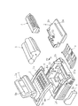
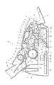
図1は、本発明の一適用対象である画像形成装置としてのレーザプリンタの主要構成部品の斜視図、図2はレーザプリンタの概略側断面図である。
メインフレーム1aの前部位とメインカバー体1bの前部位との連設部下面側には、冷却ファン35を収納するための収納部36と、記録紙Pの通過方向と直交する左右方向に延びる通風ダクト37とが連通して形成される。そして、通風ダクト37の上面板部37aを断面下向きV字状に形成し、この上面板部37aをプロセスユニット3と定着ユニット4との間に位置させて、定着ユニット4における加熱ローラ15から発生する熱がプロセスユニット3側に直接伝達しないように遮断する。
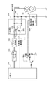
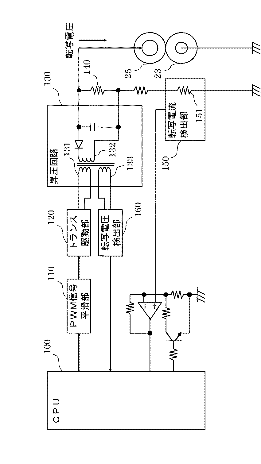
次に、本実施の形態において前記転写ローラ25に印加する転写電圧を制御する転写電圧制御部の構成について説明する。図3は、転写電圧制御部の構成の一例を示す図である。同図に示される転写電圧制御部は、CPU100を中心として構成され、CPU100から出力される転写電圧制御信号(PWMデューティ比により転写電圧の制御内容を示す。)を平滑化するPWM信号平滑部110、PWM信号平滑部110により出力されるアナログ電圧に基づいて、昇圧回路130の一次巻き線131への通電量を制御するトランス駆動部120、内部に前記一次巻き線131、二次巻き線132、及び転写電圧検出用の検出巻き線133がそれぞれ巻回されたトランスを含み、二次巻き線132に生じる電圧を転写電圧として印加することにより転写電圧印加手段の一部として機能する昇圧回路130、昇圧回路130の出力電圧を安定化させるべく設けられ、転写電圧印加手段の一部として機能している抵抗素子140、転写ローラ25と感光体ドラム23との間に流れる転写電流値を検出する転写電流検出部150、前記検出巻き線133から転写電圧値を検出する転写電圧検出部160等を含んでいる。
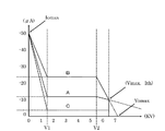
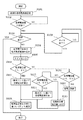
次に、本実施の形態において、検出された転写電流値及び転写電圧値から目標電流値を決定する方法について詳細に説明する。図4は、目標電流値の決定について説明するための図である。
以上、本発明の実施の形態について説明したが、本発明の内容が上記実施の形態において説明された具体例に限定されないことは勿論であり、例えば、以下のような変形例を考えることができる。
110 PWM信号平滑部
120 トランス駆動部
130 昇圧回路
131 一次巻き線
132 二次巻き線
133 検出用巻き線
140 抵抗素子
150 転写電流検出部
151 抵抗素子
160 転写電圧検出部
Claims (15)
- トナー像を担持する像担持体と、当該像担持体と対向して設けられた転写部材と、当該転写部材に転写電圧を印加する転写電圧印加手段とを備え、前記転写電圧印加手段により前記転写部材に転写電圧が印加されることにより、前記転写部材と像担持体との間に介送される記録媒体にトナー像が転写される画像形成装置において、
前記転写部材と前記像担持体との間に流れる転写電流値を検出する転写電流検出手段と、
前記転写電圧印加手段が印加している転写電圧値を検出する転写電圧検出手段と、
検出された転写電圧値及び転写電流値に基づいて制御目標とする目標電流値を決定し、当該目標電流値となるように前記転写電圧印加手段を定電流制御する制御手段とを備える
ことを特徴とする画像形成装置。 - 前記制御手段は、
検出された転写電圧値と転写電流値との比に基づいて目標電流値を決定する
ことを特徴とする請求項1に記載の画像形成装置。 - 前記制御手段は、
検出された転写電圧値及び転写電流値と目標電流値との対応関係を示すテーブルを保持するテーブル手段を備え、当該テーブル手段の内容に基づいて目標電流値を決定する
ことを特徴とする請求項1又は2に記載の画像形成装置。 - 前記制御手段は、
検出された転写電圧値及び転写電流値から、所定の数式に従って目標電流値を算出する目標電流値算出手段を備え、算出結果に従って目標電流値を決定する
ことを特徴とする請求項1又は2に記載の画像形成装置。 - 前記制御手段は、
検出された転写電圧値V0が第1の所定値V1を下回った場合において、検出された転写電流値をI0とした場合に、目標電流値を下記の(数1)により規定される電流値(I)に基づいて決定する
ことを特徴とする請求項3又は4に記載の画像形成装置。
- 前記制御手段は、
検出された転写電圧値によって目標電流値を変化させない電圧範囲における目標電流値が所定の電流値Ithを超える場合において、検出された転写電圧値V0が第2の所定値V2を上回った場合、検出された転写電流値をI0とした場合に、目標電流値を下記の(数2)により規定される電流値(I)に基づいて決定する
ことを特徴とする請求項3から5のいずれかに記載の画像形成装置。
- 前記制御手段は、
前記(数1)及び/又は(数2)において、検出された転写電圧値V0がV1とV2との間の範囲にある場合の目標電流値によりa及び/又はbの値が異なる複数の数式の中で、いずれの数式に基づいて目標電流値を決定するかを選択する選択部を有する
ことを特徴とする請求項5又は6に記載の画像形成装置。 - 前記制御手段は、
検出された転写電圧値が最大出力値Vmax以上となった場合には、定電圧制御を行う
ことを特徴とする請求項1から7のいずれかに記載の画像形成装置。 - トナー像を担持する像担持体と、当該像担持体と対向して設けられた転写部材と、当該転写部材に転写電圧を印加する転写電圧印加手段とを備え、前記転写電圧印加手段により前記転写部材に転写電圧が印加されることにより、前記転写部材と像担持体との間に介送される記録媒体にトナー像が転写される画像形成装置において、
前記転写部材と前記像担持体との間に流れる転写電流値を検出する転写電流検出手段と、
前記転写電圧印加手段が印加している転写電圧値を検出する転写電圧検出手段と、
検出された転写電圧値及び転写電流値に基づいて制御目標とする目標電圧値を決定し、当該目標電圧値となるように前記転写電圧印加手段を定電圧制御する制御手段とを備える
ことを特徴とする画像形成装置。 - 前記制御手段は、
検出された転写電圧値と転写電流値との比に基づいて目標電圧値を決定する
ことを特徴とする請求項9に記載の画像形成装置。 - 前記制御手段は、
検出された転写電圧値及び転写電流値と目標電圧値との対応関係を示すテーブルを保持するテーブル手段を備え、当該テーブル手段の内容に基づいて目標電圧値を決定する
ことを特徴とする請求項9又は10に記載の画像形成装置。 - 前記制御手段は、
検出された転写電圧値及び転写電流値から、所定の数式に従って目標電圧値を算出する目標電圧値算出手段を備え、算出結果に従って目標電圧値を決定する
ことを特徴とする請求項9又は10に記載の画像形成装置。 - 前記制御手段は、
検出された転写電圧値V0が第1の所定値V1を下回った場合において、検出された転写電流値をI0とした場合に、目標電圧値を下記の(数3)により規定される電圧値(V)に基づいて決定する
ことを特徴とする請求項11又は12に記載の画像形成装置。
- 前記制御手段は、
検出された転写電圧値によって目標電圧値を変化させない電圧範囲において設定されている所定の電流値I2が、所定の電流値Ithを超える場合において、検出された転写電圧値V0が第2の所定値V2を上回った場合、検出された転写電流値をI0とした場合に、目標電圧値を下記の(数4)により規定される電圧値(V)に基づいて決定する
ことを特徴とする請求項11から13のいずれかに記載の画像形成装置。
- 前記制御手段は、
前記(数3)及び/又は(数4)において、検出された転写電圧値V0がV1とV2との間の範囲にある場合に設定されている所定の電流値によりa及び/又はbの値が異なる複数の数式の中で、いずれの数式に基づいて目標電圧値を決定するかを選択する選択部を有する
ことを特徴とする請求項13又は14に記載の画像形成装置。
Priority Applications (2)
| Application Number | Priority Date | Filing Date | Title |
|---|---|---|---|
| JP2004103471A JP4207225B2 (ja) | 2004-03-31 | 2004-03-31 | 画像形成装置 |
| US11/092,815 US7266318B2 (en) | 2004-03-31 | 2005-03-30 | Image-forming device that performs transfer condition control |
Applications Claiming Priority (1)
| Application Number | Priority Date | Filing Date | Title |
|---|---|---|---|
| JP2004103471A JP4207225B2 (ja) | 2004-03-31 | 2004-03-31 | 画像形成装置 |
Publications (2)
| Publication Number | Publication Date |
|---|---|
| JP2005292227A true JP2005292227A (ja) | 2005-10-20 |
| JP4207225B2 JP4207225B2 (ja) | 2009-01-14 |
Family
ID=35054392
Family Applications (1)
| Application Number | Title | Priority Date | Filing Date |
|---|---|---|---|
| JP2004103471A Expired - Lifetime JP4207225B2 (ja) | 2004-03-31 | 2004-03-31 | 画像形成装置 |
Country Status (2)
| Country | Link |
|---|---|
| US (1) | US7266318B2 (ja) |
| JP (1) | JP4207225B2 (ja) |
Cited By (2)
| Publication number | Priority date | Publication date | Assignee | Title |
|---|---|---|---|---|
| JP2008129471A (ja) * | 2006-11-22 | 2008-06-05 | Canon Inc | 画像形成装置 |
| JP2009048020A (ja) * | 2007-08-21 | 2009-03-05 | Funai Electric Co Ltd | 画像投影装置、及び画像投影装置の調光制御方法 |
Families Citing this family (5)
| Publication number | Priority date | Publication date | Assignee | Title |
|---|---|---|---|---|
| JP4367285B2 (ja) * | 2004-08-09 | 2009-11-18 | ブラザー工業株式会社 | 画像形成装置 |
| JP2009157231A (ja) * | 2007-12-27 | 2009-07-16 | Brother Ind Ltd | 画像形成装置 |
| JP4666036B2 (ja) * | 2008-09-18 | 2011-04-06 | コニカミノルタビジネステクノロジーズ株式会社 | 画像形成装置 |
| JP6128871B2 (ja) * | 2013-02-05 | 2017-05-17 | キヤノン株式会社 | 画像形成装置 |
| JP2019020656A (ja) * | 2017-07-20 | 2019-02-07 | キヤノン株式会社 | 画像形成装置 |
Citations (5)
| Publication number | Priority date | Publication date | Assignee | Title |
|---|---|---|---|---|
| JPH04275583A (ja) * | 1991-03-01 | 1992-10-01 | Canon Inc | 画像形成装置 |
| JPH10301408A (ja) * | 1997-04-30 | 1998-11-13 | Fuji Xerox Co Ltd | 転写方法 |
| JP2000330401A (ja) * | 1999-05-21 | 2000-11-30 | Ricoh Co Ltd | 画像形成方法及び装置 |
| JP2002202671A (ja) * | 2000-12-28 | 2002-07-19 | Brother Ind Ltd | 画像形成装置 |
| JP2004045731A (ja) * | 2002-07-11 | 2004-02-12 | Fuji Xerox Co Ltd | 画像形成装置 |
Family Cites Families (6)
| Publication number | Priority date | Publication date | Assignee | Title |
|---|---|---|---|---|
| JP4532629B2 (ja) * | 1999-10-06 | 2010-08-25 | キヤノン株式会社 | 画像形成装置 |
| JP2001282012A (ja) * | 2000-03-31 | 2001-10-12 | Canon Inc | 画像形成装置 |
| US6442356B2 (en) * | 2000-04-06 | 2002-08-27 | Canon Kabushiki Kaisha | Image forming apparatus |
| JP2003241544A (ja) * | 2002-02-15 | 2003-08-29 | Canon Inc | 画像形成装置 |
| JP4464092B2 (ja) * | 2002-09-30 | 2010-05-19 | キヤノン株式会社 | 画像形成装置 |
| JP4393212B2 (ja) * | 2003-02-26 | 2010-01-06 | キヤノン株式会社 | 画像形成装置 |
-
2004
- 2004-03-31 JP JP2004103471A patent/JP4207225B2/ja not_active Expired - Lifetime
-
2005
- 2005-03-30 US US11/092,815 patent/US7266318B2/en not_active Expired - Lifetime
Patent Citations (5)
| Publication number | Priority date | Publication date | Assignee | Title |
|---|---|---|---|---|
| JPH04275583A (ja) * | 1991-03-01 | 1992-10-01 | Canon Inc | 画像形成装置 |
| JPH10301408A (ja) * | 1997-04-30 | 1998-11-13 | Fuji Xerox Co Ltd | 転写方法 |
| JP2000330401A (ja) * | 1999-05-21 | 2000-11-30 | Ricoh Co Ltd | 画像形成方法及び装置 |
| JP2002202671A (ja) * | 2000-12-28 | 2002-07-19 | Brother Ind Ltd | 画像形成装置 |
| JP2004045731A (ja) * | 2002-07-11 | 2004-02-12 | Fuji Xerox Co Ltd | 画像形成装置 |
Cited By (2)
| Publication number | Priority date | Publication date | Assignee | Title |
|---|---|---|---|---|
| JP2008129471A (ja) * | 2006-11-22 | 2008-06-05 | Canon Inc | 画像形成装置 |
| JP2009048020A (ja) * | 2007-08-21 | 2009-03-05 | Funai Electric Co Ltd | 画像投影装置、及び画像投影装置の調光制御方法 |
Also Published As
| Publication number | Publication date |
|---|---|
| US7266318B2 (en) | 2007-09-04 |
| US20050220472A1 (en) | 2005-10-06 |
| JP4207225B2 (ja) | 2009-01-14 |
Similar Documents
| Publication | Publication Date | Title |
|---|---|---|
| EP2107430A2 (en) | Image forming apparatus | |
| US20130223860A1 (en) | Image forming apparatus | |
| JP4207225B2 (ja) | 画像形成装置 | |
| JP4059223B2 (ja) | 電源装置及び画像形成装置 | |
| JP2009251202A (ja) | 画像形成装置 | |
| US6192213B1 (en) | Double-side printing apparatus | |
| US6064124A (en) | Power supplying apparatus for use in an image forming apparatus | |
| JPH08220816A (ja) | 画像形成装置ならびに画像形成装置の制御方法 | |
| JP4178596B2 (ja) | 画像形成装置用電源装置 | |
| JP2005287244A (ja) | 電源装置及び画像形成装置 | |
| JP4067010B2 (ja) | 電子機器 | |
| JP5155045B2 (ja) | 画像形成装置、画像形成装置の画質調整方法及びプログラム | |
| JP3915254B2 (ja) | 画像形成装置用電源装置及び画像形成装置 | |
| JP2018045046A (ja) | 画像形成装置 | |
| JPH1195606A (ja) | トナー画像定着装置 | |
| JP3166408B2 (ja) | 定着装置 | |
| JP2003167450A (ja) | 画像形成装置 | |
| JPH1195604A (ja) | トナー画像定着装置 | |
| JP4696726B2 (ja) | 電子機器 | |
| JP4706406B2 (ja) | 画像形成装置 | |
| JP4897642B2 (ja) | 画像形成装置 | |
| JP3924908B2 (ja) | 定着装置およびそれが取り付けられた画像形成装置 | |
| JPH03139682A (ja) | 定着装置 | |
| JPH11133790A (ja) | 印字装置 | |
| JP2010137481A (ja) | 光走査装置およびこれを備えた画像形成装置 |
Legal Events
| Date | Code | Title | Description |
|---|---|---|---|
| A621 | Written request for application examination |
Free format text: JAPANESE INTERMEDIATE CODE: A621 Effective date: 20050824 |
|
| A977 | Report on retrieval |
Free format text: JAPANESE INTERMEDIATE CODE: A971007 Effective date: 20080620 |
|
| A131 | Notification of reasons for refusal |
Free format text: JAPANESE INTERMEDIATE CODE: A131 Effective date: 20080711 |
|
| A521 | Request for written amendment filed |
Free format text: JAPANESE INTERMEDIATE CODE: A523 Effective date: 20080905 |
|
| TRDD | Decision of grant or rejection written | ||
| A01 | Written decision to grant a patent or to grant a registration (utility model) |
Free format text: JAPANESE INTERMEDIATE CODE: A01 Effective date: 20080929 |
|
| A01 | Written decision to grant a patent or to grant a registration (utility model) |
Free format text: JAPANESE INTERMEDIATE CODE: A01 |
|
| A61 | First payment of annual fees (during grant procedure) |
Free format text: JAPANESE INTERMEDIATE CODE: A61 Effective date: 20081012 |
|
| R150 | Certificate of patent or registration of utility model |
Ref document number: 4207225 Country of ref document: JP Free format text: JAPANESE INTERMEDIATE CODE: R150 Free format text: JAPANESE INTERMEDIATE CODE: R150 |
|
| FPAY | Renewal fee payment (event date is renewal date of database) |
Free format text: PAYMENT UNTIL: 20111031 Year of fee payment: 3 |
|
| FPAY | Renewal fee payment (event date is renewal date of database) |
Free format text: PAYMENT UNTIL: 20111031 Year of fee payment: 3 |
|
| FPAY | Renewal fee payment (event date is renewal date of database) |
Free format text: PAYMENT UNTIL: 20121031 Year of fee payment: 4 |
|
| FPAY | Renewal fee payment (event date is renewal date of database) |
Free format text: PAYMENT UNTIL: 20131031 Year of fee payment: 5 |
|
| EXPY | Cancellation because of completion of term |