JP2005291978A - Semiconductor sensor - Google Patents
Semiconductor sensor Download PDFInfo
- Publication number
- JP2005291978A JP2005291978A JP2004108639A JP2004108639A JP2005291978A JP 2005291978 A JP2005291978 A JP 2005291978A JP 2004108639 A JP2004108639 A JP 2004108639A JP 2004108639 A JP2004108639 A JP 2004108639A JP 2005291978 A JP2005291978 A JP 2005291978A
- Authority
- JP
- Japan
- Prior art keywords
- semiconductor
- diaphragm
- pressure
- ring oscillator
- sensor
- Prior art date
- Legal status (The legal status is an assumption and is not a legal conclusion. Google has not performed a legal analysis and makes no representation as to the accuracy of the status listed.)
- Pending
Links
Images


Landscapes
- Pressure Sensors (AREA)
- Measuring Fluid Pressure (AREA)
Abstract
【課題】小型で、ノイズ耐性の高い出力信号を有し、低電圧で動作する半導体圧力センサ、半導体加速度センサ、半導体応力センサを提供すること。
【解決手段】応力、圧力、加速度検出部である半導体表面にリングオシレータを形成する。それらのリングオシレータの発振するデジタル・パルス信号は、応力、圧力、加速度の変化に従って、周波数が変化する。これらのデジタル・パルス信号から応力、圧力、加速度を算出することによって、上記課題を解決する。
【選択図】図1
To provide a semiconductor pressure sensor, a semiconductor acceleration sensor, and a semiconductor stress sensor which are small in size, have an output signal with high noise resistance, and operate at a low voltage.
A ring oscillator is formed on a semiconductor surface which is a stress, pressure, and acceleration detection unit. The digital pulse signals oscillated by these ring oscillators change in frequency according to changes in stress, pressure, and acceleration. The above-described problems are solved by calculating stress, pressure, and acceleration from these digital pulse signals.
[Selection] Figure 1
Description
本発明は、CMOS回路半導体チップ中に集積する半導体圧力センサに関し、例えば、自動車タイヤ空気圧モニタに用いられる半導体圧力センサに関する。 The present invention relates to a semiconductor pressure sensor integrated in a CMOS circuit semiconductor chip, for example, a semiconductor pressure sensor used for an automobile tire pressure monitor.
自動車タイヤ空気圧不足が交通事故の一因となっていることから、自動車の安全性を高めるために、自動車タイヤ空気圧モニタ・システムは発展を続けている。自動車タイヤ空気圧が適切に保たれていれば、制動時の停止距離を伸ばしてしまうことなく、タイヤのバーストも発生しないだけでなく、燃費低下、タイヤ磨耗軽減効果もある。この自動車タイヤ空気圧モニタ・システム構成要素のひとつに、タイヤ空気圧検出用圧力センサがある。 Insufficient car tire pressure has contributed to traffic accidents, so car tire pressure monitoring systems continue to develop to increase car safety. If the vehicle tire pressure is properly maintained, the stopping distance at the time of braking is not increased, and not only the tire burst does not occur, but also the fuel consumption is reduced and the tire wear is reduced. One of the components of the automobile tire pressure monitoring system is a tire pressure detecting pressure sensor.
圧力センサの一例が特許文献1に開示されている。センサ周辺の圧力が変化すると、その周辺圧によって押されていたダイヤフラム・キャパシタの電気容量が変化する。そこで、その容量変化を電気信号として取り出し、増幅後、演算処理することで、センサ周辺圧力をモニタするという発明である。この発明の特色のひとつは、容量変化を電気信号へ変換するのに、オシレータ信号を利用しているので、耐雑音性能が高いことである。 An example of a pressure sensor is disclosed in Patent Document 1. When the pressure around the sensor changes, the capacitance of the diaphragm capacitor that has been pushed by the ambient pressure changes. Therefore, the invention is an invention in which the pressure around the sensor is monitored by taking out the capacitance change as an electric signal, performing amplification, and performing arithmetic processing. One of the features of the present invention is that noise resistance is high because an oscillator signal is used to convert a capacitance change into an electric signal.
この発明を発展させ小型化を図った発明として、特許文献2が挙げられる。この発明においては、容量変化を電気信号として取り出す回路を形成した半導体チップ中に、ダイヤフラム型キャパシタを集積すべく、キャパシタとして、ポリシリコン電極を利用している。
一方、自動車タイヤ空気圧センサは安全上、低検出精度のものは好ましくない。すなわち、ダイヤフラム・キャパシタ型自動車タイヤ空気圧センサは、安全上、十分な検出精度を保つために、十分なキャパシタ面積確保が必要となる。このため、ポリシリコン電極キャパシタタイプのセンサチップは、安全性能上、チップサイズ縮小が困難である。
On the other hand, a vehicle tire pressure sensor with low detection accuracy is not preferable for safety. That is, in the diaphragm capacitor type automobile tire pressure sensor, it is necessary to secure a sufficient capacitor area in order to maintain sufficient detection accuracy for safety. For this reason, it is difficult to reduce the chip size of the polysilicon electrode capacitor type sensor chip in terms of safety performance.
他方、センサ製造のコストパフォーマンスを上げるためには、チップサイズは小さいほど好ましい。したがって、ポリシリコン電極キャパシタタイプのセンサチップは、コストパフォーマンス向上には不向きである。更に、ポリシリコン電極をタイヤ空気圧に耐え得る厚さ(数μmオーダー)に形成すると、製造過程での熱処理条件によって、割れたり、剥がれたりするため、この圧力検出部と増幅回路や演算回路を同一のチップ上に製造するのは容易ではない。 On the other hand, in order to improve the cost performance of sensor manufacturing, it is preferable that the chip size is smaller. Therefore, the polysilicon electrode capacitor type sensor chip is not suitable for improving the cost performance. Furthermore, if the polysilicon electrode is formed to a thickness (on the order of several μm) that can withstand the tire air pressure, it will crack or peel off depending on the heat treatment conditions in the manufacturing process. It is not easy to manufacture on the chip.
チップサイズ縮小、すなわち、コストパフォーマンス向上に好適な圧力センサとしては、特許文献3が挙げられる。センサ周辺圧が変化すると、その周辺圧によって押されていたダイヤフラム型抵抗体の電気抵抗が変化する。その抵抗変化をブリッジ回路によって、電気信号として取り出し、増幅後、演算処理するという発明である。ダイヤフラム型ブリッジ抵抗体の場合、ダイヤフラム型キャパシタのような大きな面積を必要としないので、チップサイズ縮小に向いている。
As a pressure sensor suitable for chip size reduction, that is, cost performance improvement,
一方、自動車タイヤ空気圧センサは、150℃程度の高温環境にも耐えられることが要求されている。他方、ダイヤフラム型ブリッジ抵抗体センサは、小型化には向いているが、熱雑音に弱い。抵抗体自身が熱雑音発生源になるという欠点を持っているため、高温環境下での信頼性は低い。
また、半導体が歪んで結晶格子が引き伸ばされるとトランジスタの電流駆動能力が向上することが知られている(例えば、非特許文献1第14頁を参照)。
On the other hand, automobile tire pressure sensors are required to withstand a high temperature environment of about 150 ° C. On the other hand, the diaphragm type bridge resistor sensor is suitable for miniaturization, but is vulnerable to thermal noise. Since the resistor itself has a drawback of becoming a thermal noise source, its reliability in a high temperature environment is low.
Further, it is known that when a semiconductor is distorted and a crystal lattice is stretched, a current driving capability of a transistor is improved (see, for example,
CMOS回路半導体チップ中に集積できて小型化が容易なダイヤフラム型圧力センサであって、より雑音を低減できる構造のものを提供することにある。 An object of the present invention is to provide a diaphragm type pressure sensor which can be integrated in a CMOS circuit semiconductor chip and can be easily miniaturized, and has a structure capable of further reducing noise.
ダイヤフラムを半導体で形成し、当該半導体ダイヤフラム表面にリングオシレータを形成する。そのリングオシレータの発振するデジタル・パルス周波数は、圧力変化に対応して変化する。したがって、半導体ダイヤフラム表面上リングオシレータの発振するデジタル・パルス信号をデジタル演算回路に取り込み、圧力を算出する。 A diaphragm is formed of a semiconductor, and a ring oscillator is formed on the surface of the semiconductor diaphragm. The digital pulse frequency oscillated by the ring oscillator changes in response to the pressure change. Therefore, the digital pulse signal oscillated by the ring oscillator on the surface of the semiconductor diaphragm is taken into the digital arithmetic circuit to calculate the pressure.
センサ部をCMOS回路半導体チップ中に集積することにより小型化が容易である。また、半導体圧力センサのダイヤフラム部からの出力は、デジタル・パルス信号であるため、従来のアナログ出力に比べ、雑音に強くすることもできる。
さらに、ダイヤフラム部からの出力をそのままデジタル演算回路に取り込むため、従来のアナログ出力では必須だったオペレーション・アンプと増幅率規定用の高精度抵抗素子が不用となる。このため、セル数を減らすことができ、より一層、チップ小型化を可能にするという効果もある。
By integrating the sensor unit in the CMOS circuit semiconductor chip, the size can be easily reduced. Further, since the output from the diaphragm portion of the semiconductor pressure sensor is a digital pulse signal, it can be made more resistant to noise than the conventional analog output.
Further, since the output from the diaphragm section is directly taken into the digital arithmetic circuit, the operation amplifier and the high-precision resistance element for defining the amplification factor, which are essential for the conventional analog output, are unnecessary. For this reason, it is possible to reduce the number of cells and to further reduce the size of the chip.
さらに、従来のアナログ出力には必須だったオペレーション・アンプとA/D変換回路を不用にしたことで、電源電圧を下げ、消費電力低減を可能にするという効果もある。
さらに、信号処理部とセンサ部が同時に製造可能となるので、従来の半導体製造工程とコ なお、ダイヤフラム部にリングオシレータを形成する構造は、圧力センサのみならず、半導体加速度センサ、半導体応力センサにも利用可能である。
In addition, the operation amplifier and A / D conversion circuit, which are essential for conventional analog output, are eliminated, and the power supply voltage can be reduced, thereby reducing power consumption.
Furthermore, since the signal processing unit and the sensor unit can be manufactured at the same time, the structure in which the ring oscillator is formed in the diaphragm unit is not limited to the pressure sensor, but also the semiconductor acceleration sensor and the semiconductor stress sensor. Is also available.
図1は、本発明第1の実施例、半導体圧力センサ断面斜視図である。半導体基板1の裏面から基板をエッチングし、側面はすべて半導体基板1に囲まれた空洞14を形成する。半導体基板1の一部、空洞14の上部に、半導体ダイヤフラム2を設け、半導体ダイヤフラム2の表面に入力3、出力4を有するリングオシレータ5を形成した構造をしている。裏面を塞いで、空洞14を保持したまま、空洞14と周辺環境を隔絶する。そして、ある圧力環境下に置くと、圧力に従って半導体ダイヤフラム2は変形する。半導体基板1は半導体ダイヤフラム2を支持する役割と、電源回路・論理回路等を配置する役割を担っているが、本実施形態の説明においては、半導体ダイヤフラム2の詳細を述べるため、半導体基板1上の回路等は省略する。
FIG. 1 is a cross-sectional perspective view of a semiconductor pressure sensor according to a first embodiment of the present invention. The substrate is etched from the back surface of the semiconductor substrate 1 to form a
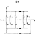
リングオシレータ5の一例を図2に示す。本例は、CMOSインバータを奇数個直列に並べて、負帰還した構造体であり、入力3より所定の電圧を印加すると、出力4からパルスが出力される。
半導体ダイヤフラム2の領域のみの模式図を図3に示す。本半導体ダイヤフラム2が圧力を受け、図4に示したように歪むと、出力4のパルスの周波数が減少する。この様子を図6に示す。図6は出力4における経過時間に対する出力電圧の変化を示している。本図に見られるように、出力は、デジタル・パルスである。図6において、実線は半導体ダイヤフラム2が圧力を受けていない状態の出力4のパルス波形を表し、点線は半導体ダイヤフラム2が圧力を受けて歪んだ状態でのリングオシレータ5からの出力4のパルス波形を表している。
An example of the
A schematic diagram of only the region of the
本図に示したようなパスル出力のパルス数を例えばカウンタ回路等で計数することで、半導体ダイヤフラム2に作用する圧力を知ることができる。すなわち、パルス・カウント数と圧力との相関関係をあらかじめテーブル化して記憶しておくことにより、圧力が算出できる。
The pressure acting on the
半導体ダイヤフラム2への圧力の向きが逆になった場合の模式図を図5に示す。図5のように半導体ダイヤフラム2が歪むと、出力4のパルス周波数が増加する。この様子を図7に示す。図7は出力4における経過時間に対する出力電圧の変化を示している。図に見られるように、出力は、デジタル・パルスである。図7において、実線は半導体ダイヤフラム2が圧力を受けていない状態の出力4のパルス波形を表し、点線は半導体ダイヤフラム2が圧力を受けて歪んだ状態でのリングオシレータ5からの出力4のパルス波形を表している。
FIG. 5 shows a schematic diagram when the direction of pressure to the
本図に示したようなパスル出力のパルス数を例えばカウンタ回路等で計数することで、半導体ダイヤフラム2に作用する圧力を知ることができる。すなわち、パルス・カウント数と圧力との相関関係をあらかじめテーブル化して記憶しておくことにより、圧力が算出できる。
The pressure acting on the
ここで、半導体ダイヤフラム2が歪むとパルス周波数が増減する理由を以下に述べる。図2に示したようなリングオシレータ5の発振するパルス周波数は、リングオシレータ5を構成するNMOSトランジスタおよびPMOSトランジスタの電流駆動能力に依存して変化する。すなわち、NMOSトランジスタまたはPMOSトランジスタの電流駆動能力が高いとリングオシレータ5の発振するパルス周波数は高くなる。逆に、NMOSトランジスタまたはPMOSトランジスタの電流駆動能力が低いとリングオシレータ5の発振するパルス周波数は低くなる。
Here, the reason why the pulse frequency increases or decreases when the
他方、半導体が歪んで結晶格子が引き伸ばされるとトランジスタの電流駆動能力が向上することが知られている(例えば、非特許文献1第14頁)。すなわち、半導体ダイヤフラム2が歪むと、半導体結晶格子は広がったり縮んだりするので、NMOSトランジスタまたはPMOSトランジスタの電流駆動能力は向上したり低下したりする。このトランジスタ電流駆動能力変化に従って、リングオシレータ5の発振するパルス周波数は増減する。
On the other hand, it is known that when a semiconductor is distorted and a crystal lattice is stretched, a current driving capability of a transistor is improved (for example, Non-Patent Document 1, page 14). In other words, when the
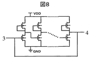
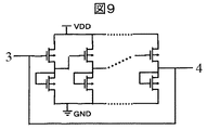
以上、図2に示したようなCMOSリングオシレータを例に説明したが、リングオシレータ5はCMOSリングオシレータではなくとも良い。例えば、図8に示すようなNMOSトランジスタのみで構成したNMOSリングオシレータや、図9に示すようなPMOSトランジスタのみで構成したPMOSリングオシレータでも、リングオシレータ5の発振パルス周波数は、半導体ダイヤフラム2の歪みに応じて、増減する。NOMSリングオシレータやPMOSリングオシレータは、CMOSリングオシレータに比べて、製造が容易であるという利点を持つが、消費電力が大きいという欠点を持っている。
As described above, the CMOS ring oscillator as shown in FIG. 2 has been described as an example, but the
本発明による半導体センサの一次出力信号は、ハイ・ローの2値デジタル電圧であるため、雑音耐性が高く、アナログ増幅器は不用である。したがって、増幅率を規定するための高精度なディスクリート抵抗素子も不用となり、半導体センサと同一チップ上に、容易に配置可能なデジタル信号処理回路を作り込むことができる。ダイヤフラム型ブリッジ抵抗体よりも、耐熱雑音性能が良く、小型化を可能にすると同時に、検出用電圧を下げることができる。 Since the primary output signal of the semiconductor sensor according to the present invention is a high / low binary digital voltage, the noise resistance is high and an analog amplifier is unnecessary. Therefore, a high-precision discrete resistance element for defining the amplification factor is also unnecessary, and a digital signal processing circuit that can be easily arranged on the same chip as the semiconductor sensor can be built. The heat resistance noise performance is better than that of the diaphragm type bridge resistor, and the detection voltage can be lowered at the same time as downsizing is possible.
本半導体センサにおいては、リングオシレータ5を構成するMOSトランジスタの個数を増やすほど、圧力センサの感度を高めることができる。すなわち、トランジスタを微細化するほど、圧力センサの感度を高めることができる。さらに、パルス数を計数する時間を長くするほど圧力センサの感度を高めることができる。
In this semiconductor sensor, the sensitivity of the pressure sensor can be increased as the number of MOS transistors constituting the
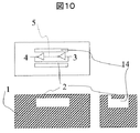
図10は、本発明第2の実施例、半導体圧力センサ平面図および側面断面図である。半導体基板1の表面から基板をエッチングし、半導体基板1の表面の一部に空洞14を形成し、半導体ダイヤフラム2を設け、半導体ダイヤフラム2の表面に入力3、出力4を有するリングオシレータ5を形成した構造をしている。表面領域のみに薄膜ガラス材料や樹脂材料を形成することで、空洞14を保持したまま、空洞14と周辺環境を隔絶する。すると、半導体ダイヤフラム部周辺圧力に従って半導体ダイヤフラム2は変形する。半導体基板1は半導体ダイヤフラム2を支持する役割と、電源回路・論理回路等を配置する役割を担っているが、本実施形態の説明においては、半導体ダイヤフラム2の詳細を述べるため、半導体基板1上の回路等は省略する。
FIG. 10 is a plan view and a side sectional view of a semiconductor pressure sensor according to a second embodiment of the present invention. The substrate is etched from the surface of the semiconductor substrate 1, a
本半導体ダイヤフラム2が圧力を受けると、図4に示したように歪み、出力4のパルスの周波数が減少する。この様子を図6に示す。図6は出力4における経過時間に対する出力電圧の変化を示している。本図に見られるように、出力は、デジタル・パルスである。図6において、実線は半導体ダイヤフラム2が圧力を受けていない状態の出力4のパルス波形を表し、点線は半導体ダイヤフラム2が圧力を受けて歪んだ状態でのリングオシレータ5からの出力4のパルス波形を表している。
When the
本図に示したようなパスル出力のパルス数を例えばカウンタ回路等で計数することで、半導体ダイヤフラム2に作用する圧力を知ることができる。すなわち、パルス・カウント数と圧力との相関関係をあらかじめテーブル化して記憶しておくことにより、圧力が算出できる。
The pressure acting on the
半導体ダイヤフラム2への圧力が負圧になった場合、半導体ダイヤフラム2は図5に示すように歪む。図5のように半導体ダイヤフラム2が歪むと、出力4のパルス周波数が増加する。この様子を図7に示す。図7は出力4における経過時間に対する出力電圧の変化を示している。図に見られるように、出力は、デジタル・パルスである。図7において、実線は半導体ダイヤフラム2が圧力を受けていない状態の出力4のパルス波形を表し、点線は半導体ダイヤフラム2が圧力を受けて歪んだ状態でのリングオシレータ5からの出力4のパルス波形を表している。
When the pressure to the
本図に示したようなパスル出力のパルス数を例えばカウンタ回路等で計数することで、半導体ダイヤフラム2に作用する圧力を知ることができる。すなわち、パルス・カウント数と圧力との相関関係をあらかじめテーブル化して記憶しておくことにより、圧力が算出できる。
半導体ダイヤフラム2が歪むとパルス周波数が増減する理由、および、リングオシレータ5の構成例は、本発明実施例1の項にて述べたので省略する。
The pressure acting on the
The reason why the pulse frequency increases / decreases when the
本発明による半導体センサの一次出力信号は、ハイ・ローの2値デジタル電圧であるため、雑音耐性が高く、アナログ増幅器は不用である。したがって、増幅率を規定するための高精度なディスクリート抵抗素子も不用となり、半導体センサと同一チップ上に、容易に配置可能なデジタル信号処理回路を作り込むことができる。ダイヤフラム型ブリッジ抵抗体よりも、耐熱雑音性能が良く、小型化を可能にすると同時に、検出用電圧を下げることができる。 Since the primary output signal of the semiconductor sensor according to the present invention is a high / low binary digital voltage, the noise resistance is high and an analog amplifier is unnecessary. Therefore, a high-precision discrete resistance element for defining the amplification factor is also unnecessary, and a digital signal processing circuit that can be easily arranged on the same chip as the semiconductor sensor can be built. The heat resistance noise performance is better than that of the diaphragm type bridge resistor, and the detection voltage can be lowered at the same time as downsizing is possible.
本半導体センサにおいては、リングオシレータ5を構成するMOSトランジスタの個数を増やすほど、圧力センサの感度を高めることができる。すなわち、トランジスタを微細化するほど、圧力センサの感度を高めることができる。さらに、パルス数を計数する時間を長くするほど圧力センサの感度を高めることができる。
In this semiconductor sensor, the sensitivity of the pressure sensor can be increased as the number of MOS transistors constituting the
図11は、本発明第3の実施例、半導体圧力センサ平面図および側面断面図である。半導体基板1の表面から基板をエッチングし、半導体基板1の表面の一部に空洞14を形成し、半導体ダイヤフラム2を設け、半導体ダイヤフラム2の表面に入力3、出力4を有するリングオシレータ5を形成した構造をしている。表面領域のみに薄膜ガラス材料や樹脂材料を形成することで、空洞14を保持したまま、空洞14と周辺環境を隔絶する。すると、半導体ダイヤフラム部周辺圧力に従って半導体ダイヤフラム2は変形する。半導体基板1は半導体ダイヤフラム2を支持する役割と、電源回路・論理回路等を配置する役割を担っているが、本実施形態の説明においては、半導体ダイヤフラム2の詳細を述べるため、半導体基板1上の回路等は省略する。
FIG. 11 is a plan view and a side sectional view of a third embodiment of the present invention, a semiconductor pressure sensor. The substrate is etched from the surface of the semiconductor substrate 1, a
本半導体ダイヤフラム2が圧力を受けると、図4に示したように歪み、出力4のパルスの周波数が減少する。この様子を図6に示す。図6は出力4における経過時間に対する出力電圧の変化を示している。本図に見られるように、出力は、デジタル・パルスである。図6において、実線は半導体ダイヤフラム2が圧力を受けていない状態の出力4のパルス波形を表し、点線は半導体ダイヤフラム2が圧力を受けて歪んだ状態でのリングオシレータ5からの出力4のパルス波形を表している。
When the
本図に示したようなパスル出力のパルス数を例えばカウンタ回路等で計数することで、半導体ダイヤフラム2に作用する圧力を知ることができる。すなわち、パルス・カウント数と圧力との相関関係をあらかじめテーブル化して記憶しておくことにより、圧力が算出できる。
The pressure acting on the
半導体ダイヤフラム2への圧力が負圧になった場合、半導体ダイヤフラム2は図5に示すように歪む。図5のように半導体ダイヤフラム2が歪むと、出力4のパルス周波数が増加する。この様子を図7に示す。図7は出力4における経過時間に対する出力電圧の変化を示している。図に見られるように、出力は、デジタル・パルスである。図7において、実線は半導体ダイヤフラム2が圧力を受けていない状態の出力4のパルス波形を表し、点線は半導体ダイヤフラム2が圧力を受けて歪んだ状態でのリングオシレータ5からの出力4のパルス波形を表している。
When the pressure to the
本図に示したようなパスル出力のパルス数を例えばカウンタ回路等で計数することで、半導体ダイヤフラム2に作用する圧力を知ることができる。すなわち、パルス・カウント数と圧力との相関関係をあらかじめテーブル化して記憶しておくことにより、圧力が算出できる。
半導体ダイヤフラム2が歪むとパルス周波数が増減する理由、および、リングオシレータ5の構成例は、本発明実施例1の項にて述べたので省略する。
The pressure acting on the
The reason why the pulse frequency increases / decreases when the
本発明による半導体センサの一次出力信号は、ハイ・ローの2値デジタル電圧であるため、雑音耐性が高く、アナログ増幅器は不用である。したがって、増幅率を規定するための高精度なディスクリート抵抗素子も不用となり、半導体センサと同一チップ上に、容易に配置可能なデジタル信号処理回路を作り込むことができる。ダイヤフラム型ブリッジ抵抗体よりも、耐熱雑音性能が良く、小型化を可能にすると同時に、検出用電圧を下げることができる。 Since the primary output signal of the semiconductor sensor according to the present invention is a high / low binary digital voltage, the noise resistance is high and an analog amplifier is unnecessary. Therefore, a high-precision discrete resistance element for defining the amplification factor is also unnecessary, and a digital signal processing circuit that can be easily arranged on the same chip as the semiconductor sensor can be built. The heat resistance noise performance is better than that of the diaphragm type bridge resistor, and the detection voltage can be lowered at the same time as downsizing is possible.
本半導体センサにおいては、リングオシレータ5を構成するMOSトランジスタの個数を増やすほど、圧力センサの感度を高めることができる。すなわち、トランジスタを微細化するほど、圧力センサの感度を高めることができる。さらに、パルス数を計数する時間を長くするほど圧力センサの感度を高めることができる。
In this semiconductor sensor, the sensitivity of the pressure sensor can be increased as the number of MOS transistors constituting the
本発明第4の実施例を以下に説明する。図11において、実施例3で述べたように半導体基板表面領域に薄膜ガラス材料や樹脂材料を形成することなく、半導体ダイヤフラム部6を錘6とすることで、図11に示した構造体は、圧力センサではなく、半導体加速度センサとなる。
A fourth embodiment of the present invention will be described below. 11, the structure shown in FIG. 11 is obtained by using the
即ち、半導体ダイヤフラム部6の製作において、圧力センサを製造する場合よりも重く造ることで、加速度に感応する錘6としての機能を持たせる。すると、錘6が加速度に従って動き、本動きに従って、半導体ダイヤフラム2は歪む。本半導体ダイヤフラム2が、図4および図5に示したように歪むと、出力4のパルスの周波数は図6および図7に示すように変化する。
That is, in the manufacture of the
図6および図7に示したようなパスル出力のパルス数を例えばカウンタ回路等で計数することで、半導体ダイヤフラム2の歪み量、並びに錘6に作用する加速度を知ることができる。すなわち、パルス・カウント数と歪み量或は加速度との相関関係をあらかじめテーブル化して記憶しておくことにより、加速度が算出できる。
半導体ダイヤフラム2が歪むとパルス周波数が増減する理由、および、リングオシレータ5の構成例は、本発明実施例1の項にて述べたので省略する。
The number of pulses of pulse output as shown in FIGS. 6 and 7 is counted by, for example, a counter circuit or the like, whereby the amount of distortion of the
The reason why the pulse frequency increases / decreases when the
本発明による半導体センサの一次出力信号は、ハイ・ローの2値デジタル電圧であるため、雑音耐性が高く、アナログ増幅器は不用である。したがって、増幅率を規定するための高精度なディスクリート抵抗素子も不用となり、半導体センサと同一チップ上に、容易に配置可能なデジタル信号処理回路を作り込むことができる。
本半導体センサにおいては、リングオシレータ5を構成するMOSトランジスタの個数を増やすほど、加速度センサの感度を高めることができる。すなわち、トランジスタを微細化するほど、加速度センサの感度を高めることができる。さらに、パルス数を計数する時間を長くするほど加速度センサの感度を高めることができる。
Since the primary output signal of the semiconductor sensor according to the present invention is a high / low binary digital voltage, the noise resistance is high and an analog amplifier is unnecessary. Therefore, a high-precision discrete resistance element for defining the amplification factor is also unnecessary, and a digital signal processing circuit that can be easily arranged on the same chip as the semiconductor sensor can be built.
In this semiconductor sensor, the sensitivity of the acceleration sensor can be increased as the number of MOS transistors constituting the
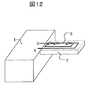
図12は、本発明第5の実施例、半導体応力センサ斜視図である。半導体1の一部に、半導体梁7を設け、半導体梁7の表面に入力3、出力4を有するリングオシレータ5を形成した構造をしている。半導体センサ部は、片持ち型半導体梁7であり、応力が加わると本半導体梁7は変形する。半導体1は半導体梁7を支持する役割と、電源回路・論理回路等を配置する役割を担っているが、本実施形態の説明においては、半導体梁7を述べるため、半導体1上の回路等は省略する。
FIG. 12 is a perspective view of a semiconductor stress sensor according to a fifth embodiment of the present invention. A
半導体梁7が応力を受け、図4および図5に示したように歪むと、出力4のパルスの周波数は図6および図7に示すように変化する。図6および図7に示したようなパスル出力のパルス数を例えばカウンタ回路等で計数することで、半導体梁7の歪み量、並びに半導体梁7に作用する応力を知ることができる。すなわち、パルス・カウント数と歪み量或は応力との相関関係をあらかじめテーブル化して記憶しておくことにより、応力が算出できる。
When the
半導体梁7が歪むとパルス周波数が増減する理由、および、リングオシレータ5の構成例は、本発明実施例1の項にて述べたので省略する。
本発明による半導体センサの一次出力信号は、ハイ・ローの2値デジタル電圧であるため、雑音耐性が高く、アナログ増幅器は不用である。したがって、増幅率を規定するための高精度なディスクリート抵抗素子も不用となり、半導体センサと同一チップ上に、容易に配置可能なデジタル信号処理回路を作り込むことができる。
The reason why the pulse frequency increases / decreases when the
Since the primary output signal of the semiconductor sensor according to the present invention is a high / low binary digital voltage, the noise resistance is high and an analog amplifier is unnecessary. Therefore, a high-precision discrete resistance element for defining the amplification factor is also unnecessary, and a digital signal processing circuit that can be easily arranged on the same chip as the semiconductor sensor can be built.
本半導体センサにおいては、リングオシレータ5を構成するMOSトランジスタの個数を増やすほど、応力センサの感度を高めることができる。すなわち、トランジスタを微細化するほど、応力センサの感度を高めることができる。さらに、パルス数を計数する時間を長くするほど応力センサの感度を高めることができる。
In this semiconductor sensor, the sensitivity of the stress sensor can be increased as the number of MOS transistors constituting the
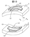
図13は、本発明第6の実施例、リングオシレータ5を構成するMOSトランジスタのチャネル形成の方向を表す図である。X方向、Y方向、Z方向を図13に示す方向とする。半導体ダイヤフラム2や半導体梁7を有する半導体センサ、すなわち半導体圧力センサ、半導体加速度センサ、半導体応力センサなどにおいて、半導体梁2が歪む方向をZ方向とする。図13上図に示したように、半導体梁2のMOSトランジスタを形成した側の表面においてY方向に引っ張り応力が作用しているような歪みにおいては、X方向がMOSトランジスタのチャネル電流方向となるように形成する。すなわち、MOSトランジスタのソース・ドレイン12と、ゲート電極13を図13に示す方向に形成することが本発明の特徴である。本方向に形成した場合、チャネル電流方向とは垂直方向(Y方向)の半導体結晶格子が引き伸ばされ、チャネル電流方向(X方向)の結晶格子間隔がチャネル全体に渡って広がり、最もトランジスタの電流駆動能力を向上させることができる。
FIG. 13 is a diagram showing the channel formation direction of the MOS transistor constituting the
逆に、図13下図に示したように、半導体梁2のMOSトランジスタを形成した側の表面においてY方向に圧縮応力が作用しているような歪みにおいては、チャネル電流方向とは垂直方向(Y方向)の半導体結晶格子が圧縮され、チャネル電流方向(X方向)の結晶格子間隔がチャネル全体に渡って縮み、最もトランジスタの電流駆動能力を低下させることができる。
On the contrary, as shown in the lower diagram of FIG. 13, in a strain in which compressive stress is acting in the Y direction on the surface of the
本図では、MOSトランジスタは1個しか記載していないが、リングオシレータ5を形成するためのMOSトランジスタ1個以上が本方向に配置されていると、リングオシレータ5の発振するパルス周波数の増減幅を大きくとることができる。このため、応力、圧力、加速度等の計測感度を高めることができる。
Although only one MOS transistor is shown in this figure, if one or more MOS transistors for forming the
圧力、加速度、応力を定量的に計測したり、定性的にセンシングするシステム全般に利用できる。特に、論理LSIへのオンチップ化、ワイヤレス・センシング・システムへの適用を可能にする低消費電力システムへ利用できる。 It can be used in general systems that measure pressure, acceleration, and stress quantitatively, or qualitatively sense. In particular, it can be used in low power consumption systems that enable on-chip logic LSIs and wireless sensing systems.
1・・・半導体基板、2・・・半導体ダイヤフラム、3・・・入力、4・・・出力、5・・・リングオシレータ、6・・・半導体ダイヤフラムあるいは錘、7・・・半導体梁、12・・・ソース・ドレイン、13・・・ゲート電極、14・・・空洞。 DESCRIPTION OF SYMBOLS 1 ... Semiconductor substrate, 2 ... Semiconductor diaphragm, 3 ... Input, 4 ... Output, 5 ... Ring oscillator, 6 ... Semiconductor diaphragm or weight, 7 ... Semiconductor beam, 12 ... source / drain, 13 ... gate electrode, 14 ... cavity.
Claims (4)
Priority Applications (1)
| Application Number | Priority Date | Filing Date | Title |
|---|---|---|---|
| JP2004108639A JP2005291978A (en) | 2004-04-01 | 2004-04-01 | Semiconductor sensor |
Applications Claiming Priority (1)
| Application Number | Priority Date | Filing Date | Title |
|---|---|---|---|
| JP2004108639A JP2005291978A (en) | 2004-04-01 | 2004-04-01 | Semiconductor sensor |
Publications (1)
| Publication Number | Publication Date |
|---|---|
| JP2005291978A true JP2005291978A (en) | 2005-10-20 |
Family
ID=35325062
Family Applications (1)
| Application Number | Title | Priority Date | Filing Date |
|---|---|---|---|
| JP2004108639A Pending JP2005291978A (en) | 2004-04-01 | 2004-04-01 | Semiconductor sensor |
Country Status (1)
| Country | Link |
|---|---|
| JP (1) | JP2005291978A (en) |
Cited By (3)
| Publication number | Priority date | Publication date | Assignee | Title |
|---|---|---|---|---|
| JP2011112419A (en) * | 2009-11-25 | 2011-06-09 | Alps Electric Co Ltd | Force sensor and method for mounting the same |
| US9089055B2 (en) | 2012-09-11 | 2015-07-21 | Seiko Epson Corporation | Electronic device, method of manufacturing the same, and oscillator |
| KR20160002489A (en) * | 2014-06-30 | 2016-01-08 | 서울시립대학교 산학협력단 | Field effective transistor typed pressure sensor and method of manufacturing the same |
Citations (4)
| Publication number | Priority date | Publication date | Assignee | Title |
|---|---|---|---|---|
| JPS5717830A (en) * | 1980-05-22 | 1982-01-29 | Siemens Ag | Semiconductor pressure sensor |
| JPH033370A (en) * | 1989-05-31 | 1991-01-09 | Honda Motor Co Ltd | Semiconductor sensor |
| JPH0310164A (en) * | 1989-06-08 | 1991-01-17 | Honda Motor Co Ltd | semiconductor sensor |
| JP2000009547A (en) * | 1998-06-22 | 2000-01-14 | Hitachi Ltd | Temperature sensor, liquid crystal display device using the same, and projection type liquid crystal display device |
-
2004
- 2004-04-01 JP JP2004108639A patent/JP2005291978A/en active Pending
Patent Citations (4)
| Publication number | Priority date | Publication date | Assignee | Title |
|---|---|---|---|---|
| JPS5717830A (en) * | 1980-05-22 | 1982-01-29 | Siemens Ag | Semiconductor pressure sensor |
| JPH033370A (en) * | 1989-05-31 | 1991-01-09 | Honda Motor Co Ltd | Semiconductor sensor |
| JPH0310164A (en) * | 1989-06-08 | 1991-01-17 | Honda Motor Co Ltd | semiconductor sensor |
| JP2000009547A (en) * | 1998-06-22 | 2000-01-14 | Hitachi Ltd | Temperature sensor, liquid crystal display device using the same, and projection type liquid crystal display device |
Cited By (4)
| Publication number | Priority date | Publication date | Assignee | Title |
|---|---|---|---|---|
| JP2011112419A (en) * | 2009-11-25 | 2011-06-09 | Alps Electric Co Ltd | Force sensor and method for mounting the same |
| US9089055B2 (en) | 2012-09-11 | 2015-07-21 | Seiko Epson Corporation | Electronic device, method of manufacturing the same, and oscillator |
| KR20160002489A (en) * | 2014-06-30 | 2016-01-08 | 서울시립대학교 산학협력단 | Field effective transistor typed pressure sensor and method of manufacturing the same |
| KR101593179B1 (en) | 2014-06-30 | 2016-02-12 | 서울시립대학교 산학협력단 | Field effective transistor typed pressure sensor and method of manufacturing the same |
Similar Documents
| Publication | Publication Date | Title |
|---|---|---|
| US8356521B2 (en) | Pressure sensor device | |
| US11604104B2 (en) | Integrated piezoresistive and piezoelectric fusion force sensor | |
| CN101458134A (en) | Semiconductor pressure sensor, method for producing the same, semiconductor device, and electronic apparatus | |
| US6167761B1 (en) | Capacitance type pressure sensor with capacitive elements actuated by a diaphragm | |
| JP5280609B2 (en) | Semiconductor device and manufacturing method thereof | |
| US7253488B2 (en) | Piezo-TFT cantilever MEMS | |
| JP5222457B2 (en) | Sensors and sensor modules | |
| JP2009068863A (en) | Infrared detector and infrared image sensor using the same | |
| JP2011158317A (en) | Pressure sensor | |
| JPWO2017068711A1 (en) | MEMS equipment | |
| JP2005291978A (en) | Semiconductor sensor | |
| US7368715B2 (en) | Semiconductor apparatus and infrared light sensor | |
| US20090283846A1 (en) | Backside controlled mems capacitive sensor and interface and method | |
| JPH10281862A (en) | Vibration type infrared sensor and manufacturing method thereof | |
| JP2014013735A (en) | Pressure switch | |
| JPH0241184B2 (en) | ||
| US8984953B2 (en) | Solid state pressure sensor | |
| US7246526B2 (en) | Pressure sensor, method of fabricating the same, and method of calibrating the same | |
| JPH03229470A (en) | Semiconductor pressure sensor | |
| JP2015155797A (en) | Thermopile, thermopile sensor using the same, and infrared sensor | |
| Weigold et al. | Thick single crystal Si lateral resonant devices integrated with a conventional circuit process | |
| Li et al. | Effects of Initial Stress on SiGe Capacitive Pressure Sensor | |
| JPH08162646A (en) | Mechanical quantity sensor | |
| JP2007292485A (en) | Pressure sensor and manufacturing method thereof | |
| JPH11304617A (en) | Semiconductor sensor |
Legal Events
| Date | Code | Title | Description |
|---|---|---|---|
| RD04 | Notification of resignation of power of attorney |
Free format text: JAPANESE INTERMEDIATE CODE: A7424 Effective date: 20060515 |
|
| A621 | Written request for application examination |
Free format text: JAPANESE INTERMEDIATE CODE: A621 Effective date: 20070329 |
|
| A977 | Report on retrieval |
Free format text: JAPANESE INTERMEDIATE CODE: A971007 Effective date: 20091225 |
|
| A131 | Notification of reasons for refusal |
Free format text: JAPANESE INTERMEDIATE CODE: A131 Effective date: 20100119 |
|
| A02 | Decision of refusal |
Free format text: JAPANESE INTERMEDIATE CODE: A02 Effective date: 20100518 |