JP2005291966A - Measuring device using surface plasmon resonance - Google Patents
Measuring device using surface plasmon resonance Download PDFInfo
- Publication number
- JP2005291966A JP2005291966A JP2004108374A JP2004108374A JP2005291966A JP 2005291966 A JP2005291966 A JP 2005291966A JP 2004108374 A JP2004108374 A JP 2004108374A JP 2004108374 A JP2004108374 A JP 2004108374A JP 2005291966 A JP2005291966 A JP 2005291966A
- Authority
- JP
- Japan
- Prior art keywords
- dielectric film
- film
- sample
- thickness
- dielectric
- Prior art date
- Legal status (The legal status is an assumption and is not a legal conclusion. Google has not performed a legal analysis and makes no representation as to the accuracy of the status listed.)
- Pending
Links
Images
Landscapes
- Investigating Or Analysing Materials By Optical Means (AREA)
- Microscoopes, Condenser (AREA)
- Investigating, Analyzing Materials By Fluorescence Or Luminescence (AREA)
Abstract
【課題】
表面プラズモン共鳴により増強された電場が表面から離れても急激に減衰しないようにすることにより測定感度を高める。
【解決手段】
非導電性基板2上に金属膜4が形成され、その上に誘電体膜6が形成されている。試料溶液8は誘電体膜6と接する。誘電体膜6の膜厚は、表面プラズモン共鳴が起こる条件で光10を基板2と金属膜4の界面に入射させたときに、光入射角と誘電体膜の厚みd2の組合せの中で、光入射角θ0が誘電体膜と試料との境界面での全反射条件角に近くなるように設定されている。
【選択図】 図4【Task】
The measurement sensitivity is enhanced by preventing the electric field enhanced by surface plasmon resonance from abruptly decaying even when the electric field leaves the surface.
[Solution]
A metal film 4 is formed on the non-conductive substrate 2, and a dielectric film 6 is formed thereon. The sample solution 8 is in contact with the dielectric film 6. The film thickness of the dielectric film 6 is selected from the combinations of the light incident angle and the thickness d 2 of the dielectric film when the light 10 is incident on the interface between the substrate 2 and the metal film 4 under the condition that surface plasmon resonance occurs. The light incident angle θ 0 is set to be close to the total reflection condition angle at the interface between the dielectric film and the sample.
[Selection] Figure 4
Description
本発明は、表面プラズモン共鳴(surface plasmon resonance)現象を用いて溶液中の物質、例えば微生物、蛋白質、核酸、糖質又はこれらが結合した混合物など、の屈折率や蛍光を測定する装置に関するものである。 The present invention relates to an apparatus for measuring the refractive index and fluorescence of substances in a solution, for example, microorganisms, proteins, nucleic acids, sugars, or a mixture in which these are bound, using a surface plasmon resonance phenomenon. is there.
表面プラズモン共鳴とは金属表面に光が入射し、表面プラズモンと同じ波数をもったエバネセント波が重なるとき、金属表面近傍の電子が共鳴状態となる現象を指す。金属又は半導体中の電子は集団的に振動しており、これはプラズマ振動又はプラズマ波と呼ばれている。表面プラズモンとは表面上のプラズマ波を量子的に述べたものである。また、エバネッセント波とは、物質の表面に沿って進行する波で、そのエネルギーが界面からの距離により指数関数的に減衰する波であって、全反射領域において入射面に沿って進行し、外部には伝播しない波をいう。 Surface plasmon resonance refers to a phenomenon in which electrons near the metal surface enter a resonance state when light is incident on the metal surface and evanescent waves having the same wave number as the surface plasmon overlap. Electrons in metals or semiconductors oscillate collectively, which is called plasma oscillation or plasma waves. A surface plasmon is a quantum description of a plasma wave on a surface. An evanescent wave is a wave that travels along the surface of a substance, whose energy exponentially decays with distance from the interface, travels along the incident surface in the total reflection region, and Refers to a wave that does not propagate.
表面プラズモン共鳴は金属表面近傍のみに感度をもつため、その領域の質量変化又は屈折率変化を高感度に捉えることができる。また、表面プラズモンが生成し表面近くに強い光電場が形成されるため、これにより表面近くに存在する物質が励起されて蛍光を発する場合には蛍光を測定することもできる。 Since surface plasmon resonance has sensitivity only in the vicinity of the metal surface, it is possible to capture a change in mass or refractive index in that region with high sensitivity. Further, since surface plasmons are generated and a strong photoelectric field is formed near the surface, when a substance existing near the surface is excited and emits fluorescence, fluorescence can be measured.
表面プラズモン共鳴を利用した測定装置は、これまで抗原抗体反応などの表面反応を利用して測定対象物を回折格子の近傍に固定化し、反射光と透過光の角度又は波長に依存したシグナル変化を測定することで、主に分子相互作用解析装置として使われてきた。 Until now, measurement devices using surface plasmon resonance have used a surface reaction such as an antigen-antibody reaction to immobilize an object to be measured in the vicinity of the diffraction grating and change the signal depending on the angle or wavelength of the reflected and transmitted light. By measuring, it has been mainly used as a molecular interaction analyzer.
表面プラズモン共鳴を励起するための光学配置のうち、最も一般的で有名なものはKretschmann配置と呼ばれるものであり、ガラスなどの非導電性基板と、その非導電性基板より誘電率の小さい層(試料や空気など)が金属膜を介して接している構造をもったものである。Kretschmann配置に光を入射すると、金属膜がない場合の全反射臨界角より大きい特定の入射角において表面プラズモン共鳴が励起される。表面プラズモン共鳴が励起されると、反射光の強度が急激に減少するので、反射光の強度をモニターすることにより共鳴条件を確認できる。 The most common and famous optical arrangement for exciting surface plasmon resonance is called the Kretschmann arrangement, which is a non-conductive substrate such as glass, and a layer with a lower dielectric constant than the non-conductive substrate ( Sample and air) are in contact with each other through a metal film. When light is incident on the Kretschmann arrangement, surface plasmon resonance is excited at a specific incident angle larger than the total reflection critical angle without the metal film. When the surface plasmon resonance is excited, the intensity of the reflected light rapidly decreases, so that the resonance condition can be confirmed by monitoring the intensity of the reflected light.
また、金属膜が酸化されたり試料溶液と反応して劣化したりするのを防いだり、蛍光分子から金属膜への蛍光共鳴エネルギー移動を防ぐことを目的として、金属膜と試料溶液との間に誘電体被覆層が設けられることがある(特許文献1参照。)が、その誘電体被覆層は、あくまで金属膜の保護膜として設けられているものであり、膜厚も保護膜としての機能を発揮するように設定されるものである。
表面プラズモン共鳴による電場の増強は金属膜の表面近くに限られ、表面から離れると急激に減衰する。そのため、試料中の被測定物質の濃度が薄い場合は感度が悪いという問題がある。
そこで、本発明は表面プラズモン共鳴により増強された電場が表面から離れても急激に減衰しないようにすることにより測定感度を高めることを目的とするものである。
The enhancement of the electric field due to surface plasmon resonance is limited to the vicinity of the surface of the metal film, and rapidly decays away from the surface. Therefore, there is a problem that the sensitivity is poor when the concentration of the substance to be measured in the sample is low.
SUMMARY OF THE INVENTION Accordingly, an object of the present invention is to increase measurement sensitivity by preventing an electric field enhanced by surface plasmon resonance from abruptly decaying even when it is separated from the surface.
本発明は、非導電性基板上に金属膜が形成され、その金属膜上に誘電体膜が形成され、その誘電体膜が試料と接する測定装置において、前記基板と金属膜との界面に表面プラズモン共鳴が起こる条件で光を入射させたとき、光入射角と誘電体膜の厚みd2の組合せの中で、光入射角θ0が誘電体膜と試料との境界面での全反射条件角に近くなるように誘電体膜の厚みd2が設定されていることを特徴とするものである。 The present invention provides a measuring apparatus in which a metal film is formed on a non-conductive substrate, a dielectric film is formed on the metal film, and the dielectric film is in contact with a sample. When light is incident under conditions where plasmon resonance occurs, among the combinations of the light incident angle and the thickness d 2 of the dielectric film, the light incident angle θ 0 is the total reflection condition at the interface between the dielectric film and the sample. The thickness d 2 of the dielectric film is set so as to be close to the corner.
ここで、「設定されている」とは、この測定装置を使用するときに誘電体膜の厚みd2がそのように設定されていることを意味している。本発明は誘電体膜の膜厚が可変のものも含んでいるので、非使用時においても常に上の条件に設定されていることを意味しているものではない。 Here, “set” means that the thickness d 2 of the dielectric film is set as such when this measuring apparatus is used. Since the present invention includes a dielectric film whose thickness is variable, it does not mean that the above conditions are always set even when not in use.
本発明が導かれる過程を説明する。非導電性基板上に金属膜が形成され、その上に誘電体膜が形成され、その誘電体膜が試料と接する系を考える。金属膜の複素誘電率が
ε1=ε1'+jε1''
で表わされ、
ε1'<0 かつ ε1''<2.5
で、金属膜の膜厚d1が
d1<100[nm]
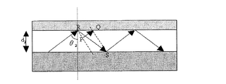
であるとき、光(直線偏光p波又はs波)の波長をλ、基板の誘電率をε0、基板内の入射角をθ0、波数をk0、膜厚をd0とし、金属膜の誘電率をε1、金属膜内の光の入射角θ1、波数をk1、膜厚をd1とし、誘電体膜の誘電率をε2、誘電体膜内の光の入射角をθ2、波数をk2、膜厚をd2とし、試料の誘電率をε3、波数をk3とし、フレネル係数の反射係数(金属膜から誘電体膜へ)r12、反射係数(誘電体膜から試料へ)r23の各々の偏角Arg[r12]=φ12、Arg[r23]=φ23、mを整数(m=1,2,・)、xを各材質の境界面方向、zを境界面に垂直な方向とすると、図1に示されるように、誘電体膜内の光導波条件より、光路長PQ=l1,RS=l2は
l2=d2/cosθ2 (1)
l1=d2sinθ2(1/tanθ2- tanθ2) (2)
から、反射における位相差も含めた2回反射の位相差pdiffは
pdiff=(k2l2+φ12+φ23)+k2l1 (3)
となる。よって誘電体膜の膜厚が(1),(2),(3)式から
<入射光p軸波のとき>
Represented by
ε 1 '<0 and ε 1 ''<2.5
The film thickness d 1 of the metal film is d 1 <100 [nm].
, The wavelength of light (linearly polarized p wave or s wave) is λ, the dielectric constant of the substrate is ε 0 , the incident angle in the substrate is θ 0 , the wave number is k 0 , the film thickness is d 0 , and the metal film The dielectric constant of the dielectric film is ε 1 , the incident angle θ 1 of light in the metal film, the wave number is k 1 , the film thickness is d 1 , the dielectric constant of the dielectric film is ε 2 , and the incident angle of light in the dielectric film is θ 2 , wave number k 2 , film thickness d 2 , sample permittivity ε 3 , wave number k 3 , Fresnel coefficient reflection coefficient (from metal film to dielectric film) r 12 , reflection coefficient (dielectric) from the body layer to the sample) each argument Arg of r 23 [r 12] = φ 12, Arg [r 23] = φ 23, m an integer (m = 1,2, ·), the x boundaries of the material When the plane direction and z are the direction perpendicular to the boundary surface, as shown in FIG. 1, the optical path lengths PQ = l 1 and RS = l 2 are l 2 = d 2 / cosθ 2 (1)
l 1 = d 2 sinθ 2 (1 / tanθ 2 -tanθ 2 ) (2)
Therefore , the phase difference p diff of the double reflection including the phase difference in the reflection is p diff = (k 2 l 2 + φ 12 + φ 23 ) + k 2 l 1 (3)
It becomes. Therefore, from the expressions (1), (2), and (3), the thickness of the dielectric film is <when incident light is p-axis>
さらに上記電場増強条件の中で光入射角と誘電体膜の厚みd2の組合せを試料内の波数k3の深さ方向成分kz3の虚数成分Imaginary(kz3)が
上に述べた「全反射条件角に近く」の「近い」の程度は、上の(4)式の条件を満たすことを意味している。
Furthermore, the imaginary component Imaginary (k z3 ) of the depth direction component k z3 of the wave number k 3 in the sample is determined by combining the light incident angle and the thickness d 2 of the dielectric film in the electric field enhancement condition.
The degree of “near” of “near the total reflection condition angle” described above means that the condition of the above equation (4) is satisfied.
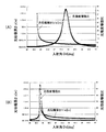
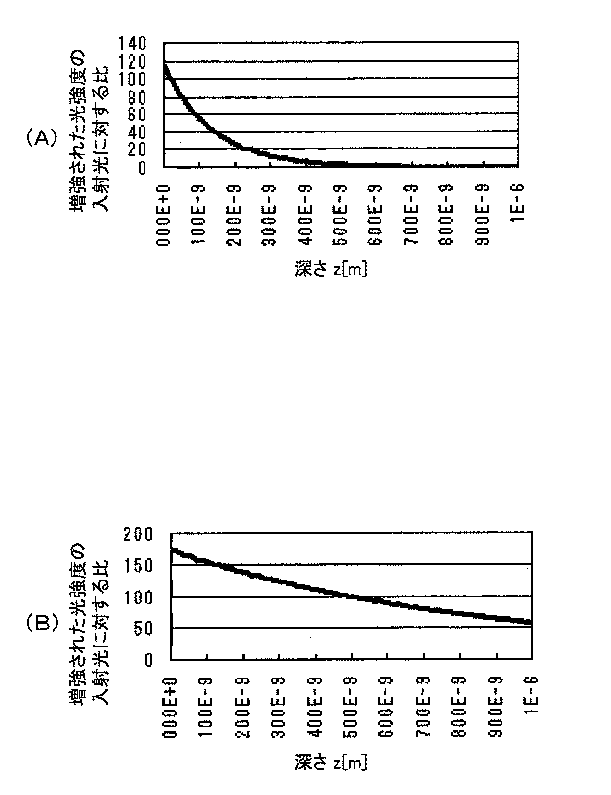
本発明における、光入射角θ0と誘電体膜の厚みd2の組合せの中で、光入射角θ0が誘電体膜と試料との境界面での全反射条件角に近くなるように誘電体膜の厚みd2を設定することの意味は、図2(B)のようになるように誘電体膜の膜厚を設定することである。図2の計算結果を導いた測定装置の構造は、石英ガラス基板上に金属膜として金を50nmの厚さに形成し、その上に誘電体膜としてシリコン酸化膜(SiO2)を形成したものである。誘電体膜と接する試料として水を想定した。同図(A)は比較例で、誘電体膜の膜厚を500nmとし、図(B)は一実施例で、誘電体膜の膜厚を400nmとしたものである。それぞれについて、光入射角θ0に対する光伝播深さと光強度増強比を計算して示している。 In the present invention, among the combinations of the light incident angle θ 0 and the thickness d 2 of the dielectric film, the dielectric is set so that the light incident angle θ 0 is close to the total reflection condition angle at the interface between the dielectric film and the sample. The meaning of setting the thickness d 2 of the body film is to set the film thickness of the dielectric film as shown in FIG. The structure of the measuring apparatus that derived the calculation result of FIG. 2 is a structure in which a gold film is formed as a metal film on a quartz glass substrate to a thickness of 50 nm, and a silicon oxide film (SiO 2 ) is formed thereon as a dielectric film. It is. Water was assumed as a sample in contact with the dielectric film. FIG. 4A is a comparative example, and the film thickness of the dielectric film is 500 nm. FIG. 4B is an example, and the film thickness of the dielectric film is 400 nm. For each, the light propagation depth and the light intensity enhancement ratio with respect to the light incident angle θ 0 are calculated and shown.
光伝播深さは次のように計算した。増強された光の伝播深さに対する光強度増強比は次の(5)式で表わされる。
図2(A),(B)の結果によれば、誘電体膜の膜厚が500nmの(A)では光入射角θ0が67.8度、光強度増強比が47倍になるが、増強された光の伝播深さは250nmにすぎない。一方、誘電体膜の膜厚が400nmの(B)では光入射角θ0が65.8度、光強度増強比が57倍で、増強された光の伝播深さは2.8μmと大きくなる。 According to the results of FIGS. 2A and 2B, the light incident angle θ 0 is 67.8 degrees and the light intensity enhancement ratio is 47 times in (A) where the film thickness of the dielectric film is 500 nm. The enhanced light propagation depth is only 250 nm. On the other hand, in (B) where the thickness of the dielectric film is 400 nm, the light incident angle θ 0 is 65.8 degrees, the light intensity enhancement ratio is 57 times, and the propagation depth of the enhanced light is as large as 2.8 μm. .
本発明の一形態では、前記誘電体膜は膜厚の異なる複数の部分を備え、それらの部分は試料への電場増強深さが互いに異なり、少なくとも1つの部分は前記条件を満たしている。
本発明の他の形態では、前記誘電体膜は金属膜側が膜厚方向に変形可能な軟質の材質、試料側がそれより硬質の材質にてなり、前記硬質の誘電体膜には圧電素子が一体として設けられ、その圧電素子により前記軟質の誘電体膜の膜厚が可変になって前記条件を満たすことができる。
In one embodiment of the present invention, the dielectric film includes a plurality of portions having different film thicknesses, and these portions have different electric field enhancement depths to the sample, and at least one portion satisfies the condition.
In another embodiment of the present invention, the dielectric film is made of a soft material that can be deformed in the film thickness direction on the metal film side and a harder material on the sample side, and a piezoelectric element is integrated with the hard dielectric film. The thickness of the soft dielectric film can be made variable by the piezoelectric element, and the condition can be satisfied.
本発明のさらに他の形態では、前記誘電体膜は金属膜側が膜厚方向に変形可能な軟質の材質、試料側がそれより硬質の材質にてなり、前記硬質の誘電体膜には加圧機構が設けられ、その加圧機構により前記軟質の誘電体膜の膜厚が可変になって前記条件を満たすことができる。
本発明のさらに他の形態では、前記誘電体膜は物理的又は化学的な特性の異なる2層の誘電体膜からなっている。
In still another embodiment of the present invention, the dielectric film is made of a soft material that can be deformed in the film thickness direction on the metal film side, and a material harder than that on the sample side. And the pressure mechanism makes the film thickness of the soft dielectric film variable to satisfy the above condition.
In still another embodiment of the present invention, the dielectric film is composed of two layers of dielectric films having different physical or chemical characteristics.
本発明によれば、金属膜上に誘電体膜が形成された、表面プラズモン共鳴を利用した測定装置で、基板と金属膜との界面に表面プラズモン共鳴が起こる条件で光を入射させたとき、光入射角と誘電体膜の厚みd2の組合せの中で、光入射角θ0が誘電体膜と試料との境界面での全反射条件角に近くなるように誘電体膜の厚みd2を設定することにより、表面プラズモン共鳴により増強された電磁場が試料の深いところまで及ぶようになり、測定の感度を高めることができる。 According to the present invention, in a measuring device using surface plasmon resonance in which a dielectric film is formed on a metal film, when light is incident on the interface between the substrate and the metal film under conditions where surface plasmon resonance occurs, among the combinations of the thickness d 2 of the light incident angle and the dielectric film, the thickness of the dielectric film such that the light incident angle theta 0 is close to the total reflection condition angle at the boundary surface between the dielectric film and the sample d 2 By setting, the electromagnetic field enhanced by surface plasmon resonance extends to the deep part of the sample, and the sensitivity of the measurement can be increased.
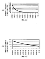
このことを電磁場シミュレーションにより確かめた結果を図3に示す。そのシミュレーションを行なった測定装置の構造は、ガラス基板(材質はBK7)上に金属膜として銀を50nmの厚さに形成し、その上に誘電体膜としてシリコン酸化膜(SiO2)を形成したものである。誘電体膜と接する試料として水を想定した。 The result of confirming this by electromagnetic field simulation is shown in FIG. The structure of the measuring apparatus that performed the simulation was that a metal film was formed with a silver thickness of 50 nm on a glass substrate (material is BK7), and a silicon oxide film (SiO 2 ) was formed thereon as a dielectric film. Is. Water was assumed as a sample in contact with the dielectric film.
図3(A)は比較例であり、誘電体膜の膜厚を500nmとした。同図(B)は一実施例であり、(1)式の条件を満たすように誘電体膜の膜厚を360nmとした。同図(A)と(B)の結果を比較すると、本発明により表面プラズモン共鳴により増強された電磁場が誘電体表面から離れると減衰する程度が小さくなっている。これにより、表面プラズモン共鳴による電磁場の存在領域が広くなり、その領域に入ってくる被測定物質も多くなるため、蛍光や屈折率を測定する際の感度が向上する。 FIG. 3A is a comparative example, and the thickness of the dielectric film was set to 500 nm. FIG. 5B shows an example, and the film thickness of the dielectric film is set to 360 nm so as to satisfy the condition of the expression (1). Comparing the results shown in FIGS. 4A and 4B, the degree to which the electromagnetic field enhanced by the surface plasmon resonance according to the present invention decays away from the dielectric surface is small. As a result, the existence region of the electromagnetic field due to surface plasmon resonance is widened, and the substance to be measured that enters the region also increases, so that the sensitivity when measuring fluorescence and refractive index is improved.
前記誘電体膜の膜厚の異なる複数の部分を備えて、それらの部分のすべて又は一部が本発明の条件を満たすようにすれば、表面プラズモン共鳴により増強された電磁場の試料側への浸透具合の異なる複数の部分を作ることができ、表面近くに存在する物質とそうでない物質の弁別が可能となる。 If a plurality of portions having different thicknesses of the dielectric film are provided and all or a part of the portions satisfy the conditions of the present invention, penetration of the electromagnetic field enhanced by surface plasmon resonance to the sample side A plurality of portions having different conditions can be formed, and a substance that exists near the surface and a substance that does not exist can be distinguished.
前記誘電体膜の膜厚を圧電素子により又は加圧機構により可変にすれば、表面プラズモン共鳴により増強された電磁場の試料側への浸透具合を変化させることができ、表面近くに存在する物質とそうでない物質の弁別が可能とする。 If the film thickness of the dielectric film is made variable by a piezoelectric element or by a pressurizing mechanism, the penetration of the electromagnetic field enhanced by surface plasmon resonance to the sample side can be changed. Allows discrimination of substances that are not.
前記誘電体膜を物理的又は化学的な特性の異なる2層の誘電体膜からなるものとすれば、例えば、試料側の誘電体膜を化学的に丈夫な膜とすることにより腐食性試料に対して有効となるなど、適用範囲が広くなる。 If the dielectric film is composed of two layers of dielectric films having different physical or chemical characteristics, for example, a corrosive sample can be obtained by making the dielectric film on the sample side chemically strong. The scope of application is widened, such as being effective against the above.
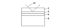
図4は第1の実施例を表わし、本発明の基本的な構造を表わしたものである。非導電性基板2上に金属膜4が形成され、その上に誘電体膜6が形成されている。試料溶液8は誘電体膜6と接する。図示は省略しているが、金属膜4と反対側の基板上には光10を表面プラズモン共鳴が起こる条件で入射させるためのプリズムが配置される。他の実施例についても同様である。
FIG. 4 shows the first embodiment and shows the basic structure of the present invention. A
この構造自体は既知のものであるが、本発明では誘電体膜6の膜厚を、表面プラズモン共鳴が起こる条件で光10を基板2と金属膜4の界面に入射させたときに(1)式を満たすように設定する。
Although this structure itself is known, in the present invention, the thickness of the
基板2は非導電性の透明物質、例えばガラス、プラスチック、石英などを用いることができる。
金属膜2の材質は一般に銀、金、銅、アルミニウムなどの高導電率材料が好適であるがこれに限らない。ただし、入射光の波長によっては、金属の電子遷移による吸収が顕著になり表面プラズモン共鳴のエネルギー密度増強効果が小さくなるので、これを避ける必要がある。その点から銀は可視域の広い波長範囲において吸収が小さく、最も好適な材料であるといえる。
誘電体膜6の材質としては、SiO2、TiO2、Al2O3などの無機誘電体材料のほか、有機透明誘電体材料を用いることもできる
The
The material of the
As a material of the
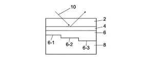
図5は第2の実施例を表わす。この実施例では誘電体膜6が膜厚の異なる複数の部分、この例では3種類の膜厚の部分6−1,6−2,6−3を備えている。このように膜厚を異ならせることで、少なくとも何れかの膜厚部分が本発明の条件を満たすようにすることが容易になる。入射光10の入射位置に対し、膜厚の異なる誘電体膜部分6−1〜6−3を相対的にスライドさせて位置決めすることにより、所望の膜厚部分で測定を行なうことができる。
FIG. 5 shows a second embodiment. In this embodiment, the
また、誘電体膜の膜厚が異なると表面プラズモン共鳴により増強された電磁場の試料側への浸透具合も異なるので、この実施例のように誘電体膜の膜厚が異なる複数の部分で測定をすることにより、表面近くに存在する物質とそうでない物質の弁別が可能となる。 In addition, since the penetration of the electromagnetic field enhanced by surface plasmon resonance to the sample side differs if the thickness of the dielectric film is different, measurement is performed at a plurality of portions where the thickness of the dielectric film is different as in this embodiment. By doing so, it becomes possible to discriminate between substances that exist near the surface and substances that do not.
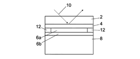
図6は第3の実施例を表わす。この実施例では、誘電体膜は金属膜4側が軟質の誘電体膜6a、試料溶液8側が硬質の誘電体膜6bからなる2層構造である。軟質の誘電体膜6aは膜厚方向に変形が可能である。硬質の誘電体膜6bと金属膜4の間には圧電素子としてピエゾ素子12が設けられており、ピエゾ素子12は電極(図示略)への電圧印加により膜厚方向の厚さを変えることができる。ピエゾ素子12の厚さの変更に伴って硬質の誘電体膜6bが変位し、軟質の誘電体膜6aの膜厚を変えることができる。
FIG. 6 shows a third embodiment. In this embodiment, the dielectric film has a two-layer structure in which the
軟質の誘電体膜6aとしては、例えばポリスチレン、ポリイミドなどの光透過性樹脂を用いることができる。硬質の誘電体膜6bとしてはガラス膜などの光透過性物質を用いることができる。
As the
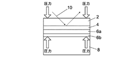
図7は第4の実施例を表わす。この実施例でも図3の実施例と同様に、誘電体膜は金属膜4側が軟質の誘電体膜6a、試料溶液8側が硬質の誘電体膜6bからなる2層構造をもっている。軟質の誘電体膜6aは膜厚が可変であり、その膜厚を変えるために、基板2と硬質の誘電体膜6bを挟んで外部から加圧する加圧機構(図示略)を備えている。その加圧機構により圧力を調整することによって軟質の誘電体膜6aの膜厚を変更する。
FIG. 7 shows a fourth embodiment. In this embodiment as well, as in the embodiment of FIG. 3, the dielectric film has a two-layer structure in which the
図6及び図7の実施例では2層の誘電体膜6a,6bの両誘電体膜6a,6bの合計膜厚が本発明の条件を満たすようにすることができる。また、誘電体膜6aの膜厚を変えて測定をすることにより表面近くに存在する物質とそうでない物質の弁別が可能となる。
6 and 7, the total thickness of the two
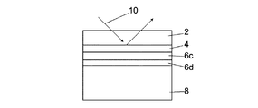
図8は第5の実施例を表わす。この実施例では誘電体膜は物理的又は化学的な特性の異なる2層の誘電体膜6c,6dからなっている。例えば、誘電体膜6cは石英ガラス、誘電体膜6dはBK7というような組合せである。また同じ材質であってもスパッタリングなどの製膜条件を制御することにより特性を異ならせることができる。特に、試料溶液8と接する誘電体膜6dは腐食性試料に対して化学的により安定な膜とすることが好ましい。
FIG. 8 shows a fifth embodiment. In this embodiment, the dielectric film is composed of two
本発明の測定装置は、試料の屈折率や蛍光を測定する装置として、又は液体クロマトグラフやキャピラリ電気泳動などの分析装置の検出器として用いて屈折率や蛍光を介して試料成分の濃度を測定する装置として利用することができる。 The measuring device of the present invention is used as a device for measuring the refractive index and fluorescence of a sample, or as a detector of an analytical device such as a liquid chromatograph or capillary electrophoresis, and measures the concentration of a sample component via the refractive index or fluorescence. It can be used as a device to perform.
2 基板
4 金属膜
6,6a,6b,6c,6d 誘電体膜
8 試料溶液
10 光
12 ピエゾ素子
2
Claims (5)
前記基板と金属膜との界面に表面プラズモン共鳴が起こる条件で光を入射させたとき、光入射角と誘電体膜の厚みd2の組合せの中で、光入射角θ0が誘電体膜と試料との境界面での全反射条件角に近くなるように誘電体膜の厚みd2が設定されていることを特徴とする測定装置。 In a measuring apparatus in which a metal film is formed on a non-conductive substrate, a dielectric film is formed on the metal film, and the dielectric film is in contact with the sample.
When light is incident on the interface between the substrate and the metal film under the condition that surface plasmon resonance occurs, among the combinations of the light incident angle and the thickness d 2 of the dielectric film, the light incident angle θ 0 is A measuring apparatus, wherein a thickness d 2 of the dielectric film is set so as to be close to a total reflection condition angle at a boundary surface with a sample.
2. The measuring apparatus according to claim 1, wherein the dielectric film is a two-layer dielectric film having different physical or chemical characteristics.
Priority Applications (1)
| Application Number | Priority Date | Filing Date | Title |
|---|---|---|---|
| JP2004108374A JP2005291966A (en) | 2004-03-31 | 2004-03-31 | Measuring device using surface plasmon resonance |
Applications Claiming Priority (1)
| Application Number | Priority Date | Filing Date | Title |
|---|---|---|---|
| JP2004108374A JP2005291966A (en) | 2004-03-31 | 2004-03-31 | Measuring device using surface plasmon resonance |
Publications (1)
| Publication Number | Publication Date |
|---|---|
| JP2005291966A true JP2005291966A (en) | 2005-10-20 |
Family
ID=35325050
Family Applications (1)
| Application Number | Title | Priority Date | Filing Date |
|---|---|---|---|
| JP2004108374A Pending JP2005291966A (en) | 2004-03-31 | 2004-03-31 | Measuring device using surface plasmon resonance |
Country Status (1)
| Country | Link |
|---|---|
| JP (1) | JP2005291966A (en) |
Cited By (9)
| Publication number | Priority date | Publication date | Assignee | Title |
|---|---|---|---|---|
| JP2007271597A (en) * | 2006-03-09 | 2007-10-18 | National Institute Of Advanced Industrial & Technology | Optical guided mode sensor |
| JP2008046093A (en) * | 2006-08-21 | 2008-02-28 | National Institute Of Advanced Industrial & Technology | Optical waveguide mode sensor with pores |
| JP2008224561A (en) * | 2007-03-15 | 2008-09-25 | Fujifilm Corp | Surface plasmon enhanced fluorescence sensor |
| JP2010181323A (en) * | 2009-02-06 | 2010-08-19 | Konica Minolta Holdings Inc | Assay method using surface plasmon |
| WO2011115445A3 (en) * | 2010-03-19 | 2012-02-09 | 경원대학교 산학협력단 | Biochip |
| JP2012032281A (en) * | 2010-07-30 | 2012-02-16 | Konica Minolta Holdings Inc | Plasmon excitation sensor and assay method using the same sensor |
| US9081005B2 (en) | 2010-03-19 | 2015-07-14 | Gachon University Industry University Cooperation Foundation | Biochip |
| WO2016093037A1 (en) * | 2014-12-09 | 2016-06-16 | コニカミノルタ株式会社 | Detection device and detection method |
| WO2016093039A1 (en) * | 2014-12-09 | 2016-06-16 | コニカミノルタ株式会社 | Detection chip and detection method |
-
2004
- 2004-03-31 JP JP2004108374A patent/JP2005291966A/en active Pending
Cited By (12)
| Publication number | Priority date | Publication date | Assignee | Title |
|---|---|---|---|---|
| JP2007271597A (en) * | 2006-03-09 | 2007-10-18 | National Institute Of Advanced Industrial & Technology | Optical guided mode sensor |
| JP2008046093A (en) * | 2006-08-21 | 2008-02-28 | National Institute Of Advanced Industrial & Technology | Optical waveguide mode sensor with pores |
| JP2008224561A (en) * | 2007-03-15 | 2008-09-25 | Fujifilm Corp | Surface plasmon enhanced fluorescence sensor |
| JP2010181323A (en) * | 2009-02-06 | 2010-08-19 | Konica Minolta Holdings Inc | Assay method using surface plasmon |
| WO2011115445A3 (en) * | 2010-03-19 | 2012-02-09 | 경원대학교 산학협력단 | Biochip |
| US9081005B2 (en) | 2010-03-19 | 2015-07-14 | Gachon University Industry University Cooperation Foundation | Biochip |
| JP2012032281A (en) * | 2010-07-30 | 2012-02-16 | Konica Minolta Holdings Inc | Plasmon excitation sensor and assay method using the same sensor |
| WO2016093037A1 (en) * | 2014-12-09 | 2016-06-16 | コニカミノルタ株式会社 | Detection device and detection method |
| WO2016093039A1 (en) * | 2014-12-09 | 2016-06-16 | コニカミノルタ株式会社 | Detection chip and detection method |
| JPWO2016093039A1 (en) * | 2014-12-09 | 2017-09-14 | コニカミノルタ株式会社 | Detection chip and detection method |
| JPWO2016093037A1 (en) * | 2014-12-09 | 2017-09-14 | コニカミノルタ株式会社 | Detection apparatus and detection method |
| US10254228B2 (en) | 2014-12-09 | 2019-04-09 | Konica Minolta, Inc. | Detection chip and detection method |
Similar Documents
| Publication | Publication Date | Title |
|---|---|---|
| US7671995B2 (en) | Method for improving surface plasmon resonance by using conducting metal oxide as adhesive layer | |
| US7349598B2 (en) | Surface plasmon resonance device | |
| EP0570445B1 (en) | Analytical device | |
| EP2450692B1 (en) | High sensitivity localized surface plasmon resonance sensor and sensor system using same | |
| Paliwal et al. | Refractive index sensor using long-range surface plasmon resonance with prism coupler | |
| US8786859B2 (en) | High resolution surface plasmon resonance sensor and sensor system thereof | |
| Sun et al. | Self-referenced refractive index sensor based on hybrid mode resonances in 2D metal-dielectric grating | |
| Mohanty et al. | Effect of semiconductor on sensitivity of a graphene-based surface plasmon resonance biosensor | |
| EP2331940B1 (en) | Optical detection sysytem comprising an assembly with absorbing sensor layer | |
| CN107064078B (en) | Optical sensor based on BSW and optical detection method | |
| Houari et al. | Engineering and optimization of the spr device zno/ag/wo3/ni/2d-nanomaterials highly sensitive for biomedical processing and detection | |
| CN109001157A (en) | A method of refractive index sensing is realized based on duplex surface plasma resonance | |
| Singh et al. | Sensitivity enhancement of SPR biosensor employing heterostructure blue phosphorus/MoS2 and silicon layer | |
| JP7178664B2 (en) | Electrical measurement type surface plasmon resonance sensor and electrical measurement type surface plasmon resonance sensor chip used therefor | |
| JP2005291966A (en) | Measuring device using surface plasmon resonance | |
| El Barghouti et al. | High-performance bimetallic layer plasmonic sensors: a comparative study among Ti 3 C 2 T x, black phosphorus and WS 2 | |
| Jamil et al. | Graphene-MoS 2 SPR-based biosensor for urea detection | |
| Lee et al. | Parametric study on the bimetallic waveguide coupled surface plasmon resonance sensors in comparison with other configurations | |
| Singh et al. | Investigation of SPR sensor for immunoglobulin detection by using Ag–Si 3 N 4-BP on the sensing layer | |
| Pandey et al. | Investigating the performance of metal-assisted guided mode resonance based structures for biosensing applications | |
| Alaaudeen et al. | Design and modelling of surface plasmon resonance biosensor employing BaTiO3 and graphene nanostructure for detection of SARS-CoV-2 virus | |
| Rafsan et al. | Surface plasmon resonance–based biosensor for accurate and rapid detection of Mycobacterium tuberculosis | |
| TW201305549A (en) | Metal buffer layer assisted guided mode resonance biosensor | |
| TWI481855B (en) | Surface plasmon resonance detection system with multilayer film structure | |
| Saad et al. | Theoretical evaluation of a fiber-optic SPR biosensor based on a gold layer treated with thiol acid |
Legal Events
| Date | Code | Title | Description |
|---|---|---|---|
| A621 | Written request for application examination |
Free format text: JAPANESE INTERMEDIATE CODE: A621 Effective date: 20060607 |
|
| A977 | Report on retrieval |
Free format text: JAPANESE INTERMEDIATE CODE: A971007 Effective date: 20080401 |
|
| A131 | Notification of reasons for refusal |
Effective date: 20080513 Free format text: JAPANESE INTERMEDIATE CODE: A131 |
|
| A02 | Decision of refusal |
Effective date: 20080930 Free format text: JAPANESE INTERMEDIATE CODE: A02 |