JP2005291886A - Manufacturing method of humidity sensor element, and the humidity sensor element - Google Patents
Manufacturing method of humidity sensor element, and the humidity sensor element Download PDFInfo
- Publication number
- JP2005291886A JP2005291886A JP2004106683A JP2004106683A JP2005291886A JP 2005291886 A JP2005291886 A JP 2005291886A JP 2004106683 A JP2004106683 A JP 2004106683A JP 2004106683 A JP2004106683 A JP 2004106683A JP 2005291886 A JP2005291886 A JP 2005291886A
- Authority
- JP
- Japan
- Prior art keywords
- humidity sensor
- sensor element
- sensitive film
- moisture sensitive
- insulating substrate
- Prior art date
- Legal status (The legal status is an assumption and is not a legal conclusion. Google has not performed a legal analysis and makes no representation as to the accuracy of the status listed.)
- Withdrawn
Links
- 238000004519 manufacturing process Methods 0.000 title claims abstract description 26
- 239000000758 substrate Substances 0.000 claims abstract description 71
- 239000006185 dispersion Substances 0.000 abstract 1
- 238000005192 partition Methods 0.000 description 37
- 238000000034 method Methods 0.000 description 30
- 239000000463 material Substances 0.000 description 28
- 239000000243 solution Substances 0.000 description 25
- -1 polytetrafluoroethylene Polymers 0.000 description 16
- 238000005520 cutting process Methods 0.000 description 13
- XLYOFNOQVPJJNP-UHFFFAOYSA-N water Substances O XLYOFNOQVPJJNP-UHFFFAOYSA-N 0.000 description 13
- 230000008859 change Effects 0.000 description 12
- 230000000052 comparative effect Effects 0.000 description 12
- 230000008569 process Effects 0.000 description 10
- 230000008961 swelling Effects 0.000 description 9
- 238000000576 coating method Methods 0.000 description 8
- 150000001875 compounds Chemical class 0.000 description 8
- WABPQHHGFIMREM-UHFFFAOYSA-N lead(0) Chemical compound [Pb] WABPQHHGFIMREM-UHFFFAOYSA-N 0.000 description 8
- 229910052757 nitrogen Inorganic materials 0.000 description 7
- OKKJLVBELUTLKV-UHFFFAOYSA-N Methanol Chemical compound OC OKKJLVBELUTLKV-UHFFFAOYSA-N 0.000 description 6
- 229920001940 conductive polymer Polymers 0.000 description 6
- 239000004033 plastic Substances 0.000 description 6
- 229920003023 plastic Polymers 0.000 description 6
- 229910000077 silane Inorganic materials 0.000 description 6
- 229910000679 solder Inorganic materials 0.000 description 6
- 239000006087 Silane Coupling Agent Substances 0.000 description 5
- 239000000178 monomer Substances 0.000 description 5
- 125000004433 nitrogen atom Chemical group N* 0.000 description 5
- 229920001343 polytetrafluoroethylene Polymers 0.000 description 5
- 239000004810 polytetrafluoroethylene Substances 0.000 description 5
- 239000000126 substance Substances 0.000 description 5
- CSCPPACGZOOCGX-UHFFFAOYSA-N Acetone Chemical compound CC(C)=O CSCPPACGZOOCGX-UHFFFAOYSA-N 0.000 description 4
- 239000011248 coating agent Substances 0.000 description 4
- 229920001577 copolymer Polymers 0.000 description 4
- 239000010949 copper Substances 0.000 description 4
- 238000006073 displacement reaction Methods 0.000 description 4
- 230000002349 favourable effect Effects 0.000 description 4
- 239000011521 glass Substances 0.000 description 4
- 150000002500 ions Chemical class 0.000 description 4
- 239000002244 precipitate Substances 0.000 description 4
- 238000007650 screen-printing Methods 0.000 description 4
- XDLMVUHYZWKMMD-UHFFFAOYSA-N 3-trimethoxysilylpropyl 2-methylprop-2-enoate Chemical compound CO[Si](OC)(OC)CCCOC(=O)C(C)=C XDLMVUHYZWKMMD-UHFFFAOYSA-N 0.000 description 3
- QTBSBXVTEAMEQO-UHFFFAOYSA-N Acetic acid Chemical compound CC(O)=O QTBSBXVTEAMEQO-UHFFFAOYSA-N 0.000 description 3
- RYGMFSIKBFXOCR-UHFFFAOYSA-N Copper Chemical compound [Cu] RYGMFSIKBFXOCR-UHFFFAOYSA-N 0.000 description 3
- KFZMGEQAYNKOFK-UHFFFAOYSA-N Isopropanol Chemical compound CC(C)O KFZMGEQAYNKOFK-UHFFFAOYSA-N 0.000 description 3
- 230000015572 biosynthetic process Effects 0.000 description 3
- 239000000470 constituent Substances 0.000 description 3
- 229910052802 copper Inorganic materials 0.000 description 3
- 238000004132 cross linking Methods 0.000 description 3
- 238000001035 drying Methods 0.000 description 3
- 239000007789 gas Substances 0.000 description 3
- 239000007788 liquid Substances 0.000 description 3
- 230000000630 rising effect Effects 0.000 description 3
- YHRUOJUYPBUZOS-UHFFFAOYSA-N 1,3-dichloropropane Chemical compound ClCCCCl YHRUOJUYPBUZOS-UHFFFAOYSA-N 0.000 description 2
- FLCAEMBIQVZWIF-UHFFFAOYSA-N 6-(dimethylamino)-2-methylhex-2-enamide Chemical compound CN(C)CCCC=C(C)C(N)=O FLCAEMBIQVZWIF-UHFFFAOYSA-N 0.000 description 2
- CBENFWSGALASAD-UHFFFAOYSA-N Ozone Chemical compound [O-][O+]=O CBENFWSGALASAD-UHFFFAOYSA-N 0.000 description 2
- 239000002033 PVDF binder Substances 0.000 description 2
- 239000004813 Perfluoroalkoxy alkane Substances 0.000 description 2
- BQCADISMDOOEFD-UHFFFAOYSA-N Silver Chemical compound [Ag] BQCADISMDOOEFD-UHFFFAOYSA-N 0.000 description 2
- 125000000217 alkyl group Chemical group 0.000 description 2
- PNEYBMLMFCGWSK-UHFFFAOYSA-N aluminium oxide Inorganic materials [O-2].[O-2].[O-2].[Al+3].[Al+3] PNEYBMLMFCGWSK-UHFFFAOYSA-N 0.000 description 2
- 150000001450 anions Chemical class 0.000 description 2
- 238000007598 dipping method Methods 0.000 description 2
- SNRUBQQJIBEYMU-UHFFFAOYSA-N dodecane Chemical compound CCCCCCCCCCCC SNRUBQQJIBEYMU-UHFFFAOYSA-N 0.000 description 2
- 238000011156 evaluation Methods 0.000 description 2
- 230000004907 flux Effects 0.000 description 2
- 239000010931 gold Substances 0.000 description 2
- 125000002887 hydroxy group Chemical group [H]O* 0.000 description 2
- 230000006872 improvement Effects 0.000 description 2
- 230000000873 masking effect Effects 0.000 description 2
- 229910052751 metal Inorganic materials 0.000 description 2
- 239000002184 metal Substances 0.000 description 2
- 239000000203 mixture Substances 0.000 description 2
- KDLHZDBZIXYQEI-UHFFFAOYSA-N palladium Substances [Pd] KDLHZDBZIXYQEI-UHFFFAOYSA-N 0.000 description 2
- 229920011301 perfluoro alkoxyl alkane Polymers 0.000 description 2
- BASFCYQUMIYNBI-UHFFFAOYSA-N platinum Substances [Pt] BASFCYQUMIYNBI-UHFFFAOYSA-N 0.000 description 2
- 229920000642 polymer Polymers 0.000 description 2
- 229920002981 polyvinylidene fluoride Polymers 0.000 description 2
- 239000000047 product Substances 0.000 description 2
- 238000001226 reprecipitation Methods 0.000 description 2
- WOCIAKWEIIZHES-UHFFFAOYSA-N ruthenium(iv) oxide Chemical compound O=[Ru]=O WOCIAKWEIIZHES-UHFFFAOYSA-N 0.000 description 2
- 230000035945 sensitivity Effects 0.000 description 2
- 229910052709 silver Inorganic materials 0.000 description 2
- 239000004332 silver Substances 0.000 description 2
- 230000002194 synthesizing effect Effects 0.000 description 2
- RNXPZVYZVHJVHM-UHFFFAOYSA-N 1,12-dichlorododecane Chemical compound ClCCCCCCCCCCCCCl RNXPZVYZVHJVHM-UHFFFAOYSA-N 0.000 description 1
- VEFLKXRACNJHOV-UHFFFAOYSA-N 1,3-dibromopropane Chemical compound BrCCCBr VEFLKXRACNJHOV-UHFFFAOYSA-N 0.000 description 1
- JKNCOURZONDCGV-UHFFFAOYSA-N 2-(dimethylamino)ethyl 2-methylprop-2-enoate Chemical compound CN(C)CCOC(=O)C(C)=C JKNCOURZONDCGV-UHFFFAOYSA-N 0.000 description 1
- DPBJAVGHACCNRL-UHFFFAOYSA-N 2-(dimethylamino)ethyl prop-2-enoate Chemical compound CN(C)CCOC(=O)C=C DPBJAVGHACCNRL-UHFFFAOYSA-N 0.000 description 1
- ZNQVEEAIQZEUHB-UHFFFAOYSA-N 2-ethoxyethanol Chemical compound CCOCCO ZNQVEEAIQZEUHB-UHFFFAOYSA-N 0.000 description 1
- DOYKFSOCSXVQAN-UHFFFAOYSA-N 3-[diethoxy(methyl)silyl]propyl 2-methylprop-2-enoate Chemical compound CCO[Si](C)(OCC)CCCOC(=O)C(C)=C DOYKFSOCSXVQAN-UHFFFAOYSA-N 0.000 description 1
- LZMNXXQIQIHFGC-UHFFFAOYSA-N 3-[dimethoxy(methyl)silyl]propyl 2-methylprop-2-enoate Chemical compound CO[Si](C)(OC)CCCOC(=O)C(C)=C LZMNXXQIQIHFGC-UHFFFAOYSA-N 0.000 description 1
- URDOJQUSEUXVRP-UHFFFAOYSA-N 3-triethoxysilylpropyl 2-methylprop-2-enoate Chemical compound CCO[Si](OCC)(OCC)CCCOC(=O)C(C)=C URDOJQUSEUXVRP-UHFFFAOYSA-N 0.000 description 1
- KBQVDAIIQCXKPI-UHFFFAOYSA-N 3-trimethoxysilylpropyl prop-2-enoate Chemical compound CO[Si](OC)(OC)CCCOC(=O)C=C KBQVDAIIQCXKPI-UHFFFAOYSA-N 0.000 description 1
- CPELXLSAUQHCOX-UHFFFAOYSA-M Bromide Chemical compound [Br-] CPELXLSAUQHCOX-UHFFFAOYSA-M 0.000 description 1
- 229910000906 Bronze Inorganic materials 0.000 description 1
- VEXZGXHMUGYJMC-UHFFFAOYSA-M Chloride anion Chemical compound [Cl-] VEXZGXHMUGYJMC-UHFFFAOYSA-M 0.000 description 1
- LFQSCWFLJHTTHZ-UHFFFAOYSA-N Ethanol Chemical compound CCO LFQSCWFLJHTTHZ-UHFFFAOYSA-N 0.000 description 1
- KRHYYFGTRYWZRS-UHFFFAOYSA-M Fluoride anion Chemical compound [F-] KRHYYFGTRYWZRS-UHFFFAOYSA-M 0.000 description 1
- YCKRFDGAMUMZLT-UHFFFAOYSA-N Fluorine atom Chemical compound [F] YCKRFDGAMUMZLT-UHFFFAOYSA-N 0.000 description 1
- OAICVXFJPJFONN-UHFFFAOYSA-N Phosphorus Chemical compound [P] OAICVXFJPJFONN-UHFFFAOYSA-N 0.000 description 1
- 239000004642 Polyimide Substances 0.000 description 1
- 239000004809 Teflon Substances 0.000 description 1
- 229920006362 Teflon® Polymers 0.000 description 1
- IHWJXGQYRBHUIF-UHFFFAOYSA-N [Ag].[Pt] Chemical compound [Ag].[Pt] IHWJXGQYRBHUIF-UHFFFAOYSA-N 0.000 description 1
- 125000003647 acryloyl group Chemical group O=C([*])C([H])=C([H])[H] 0.000 description 1
- 125000005370 alkoxysilyl group Chemical group 0.000 description 1
- 229910045601 alloy Inorganic materials 0.000 description 1
- 239000000956 alloy Substances 0.000 description 1
- 238000013459 approach Methods 0.000 description 1
- 239000007864 aqueous solution Substances 0.000 description 1
- 230000001174 ascending effect Effects 0.000 description 1
- 229940006460 bromide ion Drugs 0.000 description 1
- 239000010974 bronze Substances 0.000 description 1
- 239000000919 ceramic Substances 0.000 description 1
- 238000006243 chemical reaction Methods 0.000 description 1
- KUNSUQLRTQLHQQ-UHFFFAOYSA-N copper tin Chemical compound [Cu].[Sn] KUNSUQLRTQLHQQ-UHFFFAOYSA-N 0.000 description 1
- 230000006866 deterioration Effects 0.000 description 1
- 239000012153 distilled water Substances 0.000 description 1
- 238000004453 electron probe microanalysis Methods 0.000 description 1
- 239000003822 epoxy resin Substances 0.000 description 1
- FWDBOZPQNFPOLF-UHFFFAOYSA-N ethenyl(triethoxy)silane Chemical compound CCO[Si](OCC)(OCC)C=C FWDBOZPQNFPOLF-UHFFFAOYSA-N 0.000 description 1
- NKSJNEHGWDZZQF-UHFFFAOYSA-N ethenyl(trimethoxy)silane Chemical compound CO[Si](OC)(OC)C=C NKSJNEHGWDZZQF-UHFFFAOYSA-N 0.000 description 1
- 229910052731 fluorine Inorganic materials 0.000 description 1
- 239000011737 fluorine Substances 0.000 description 1
- 229920002313 fluoropolymer Polymers 0.000 description 1
- 239000004811 fluoropolymer Substances 0.000 description 1
- 125000000524 functional group Chemical group 0.000 description 1
- PCHJSUWPFVWCPO-UHFFFAOYSA-N gold Chemical compound [Au] PCHJSUWPFVWCPO-UHFFFAOYSA-N 0.000 description 1
- 229910052737 gold Inorganic materials 0.000 description 1
- 238000007646 gravure printing Methods 0.000 description 1
- 238000010438 heat treatment Methods 0.000 description 1
- 238000007654 immersion Methods 0.000 description 1
- 229920000831 ionic polymer Polymers 0.000 description 1
- 229910044991 metal oxide Inorganic materials 0.000 description 1
- 150000004706 metal oxides Chemical class 0.000 description 1
- TXXWBTOATXBWDR-UHFFFAOYSA-N n,n,n',n'-tetramethylhexane-1,6-diamine Chemical compound CN(C)CCCCCCN(C)C TXXWBTOATXBWDR-UHFFFAOYSA-N 0.000 description 1
- 239000012299 nitrogen atmosphere Substances 0.000 description 1
- 229910052763 palladium Inorganic materials 0.000 description 1
- FYJQJMIEZVMYSD-UHFFFAOYSA-N perfluoro-2-butyltetrahydrofuran Chemical compound FC(F)(F)C(F)(F)C(F)(F)C(F)(F)C1(F)OC(F)(F)C(F)(F)C1(F)F FYJQJMIEZVMYSD-UHFFFAOYSA-N 0.000 description 1
- 230000002093 peripheral effect Effects 0.000 description 1
- 239000005011 phenolic resin Substances 0.000 description 1
- 239000004014 plasticizer Substances 0.000 description 1
- 229910052697 platinum Inorganic materials 0.000 description 1
- 229920000647 polyepoxide Polymers 0.000 description 1
- 229920001721 polyimide Polymers 0.000 description 1
- 239000003505 polymerization initiator Substances 0.000 description 1
- 239000010453 quartz Substances 0.000 description 1
- 230000009257 reactivity Effects 0.000 description 1
- 229920005989 resin Polymers 0.000 description 1
- 239000011347 resin Substances 0.000 description 1
- 229910001925 ruthenium oxide Inorganic materials 0.000 description 1
- 229920006395 saturated elastomer Polymers 0.000 description 1
- 229910052710 silicon Inorganic materials 0.000 description 1
- 239000010703 silicon Substances 0.000 description 1
- VYPSYNLAJGMNEJ-UHFFFAOYSA-N silicon dioxide Inorganic materials O=[Si]=O VYPSYNLAJGMNEJ-UHFFFAOYSA-N 0.000 description 1
- 238000005245 sintering Methods 0.000 description 1
- 239000002904 solvent Substances 0.000 description 1
- 229920002554 vinyl polymer Polymers 0.000 description 1
Images
Landscapes
- Investigating Or Analyzing Materials By The Use Of Fluid Adsorption Or Reactions (AREA)
- Investigating Or Analyzing Materials By The Use Of Electric Means (AREA)
Abstract
Description
本発明は、湿度センサ素子の製造方法及び湿度センサ素子に係り、より詳細には抵抗変化型湿度センサ素子の製造方法及び湿度センサ素子に関する。 The present invention relates to a humidity sensor element manufacturing method and a humidity sensor element, and more particularly to a resistance change type humidity sensor element manufacturing method and a humidity sensor element.
気体中の相対湿度の変化を電気抵抗の変化として湿度の値を測定する抵抗変化型湿度センサ素子が知られている。この抵抗変化型湿度センサ素子は一般に、絶縁基板と、絶縁基板の一面上に形成される一対の電極と、一対の電極上に設けられる感湿膜とを備えている。 2. Description of the Related Art A resistance change type humidity sensor element that measures a humidity value using a change in relative humidity in gas as a change in electrical resistance is known. This resistance change type humidity sensor element generally includes an insulating substrate, a pair of electrodes formed on one surface of the insulating substrate, and a moisture sensitive film provided on the pair of electrodes.
このような湿度センサ素子の製造方法として、絶縁基板上の一対の電極の周囲にダムを形成し、このダムの内側であって絶縁基板上に感湿膜を形成することにより、感湿膜の膜厚が十分で感度が高い湿度センサ素子を作製する方法が提案されている(例えば特許文献1参照)。
本発明者らは、前述した特許文献1に記載の湿度センサ素子では、得られる湿度センサ素子ごとの初期出力のバラツキを小さくできるものの、製造歩留まりをより一層向上させる観点からは、この初期出力のバラツキについて未だ改良の余地があることを見出した。さらに、本発明者らは、このような初期出力のバラツキが、上記ダムを形成しない場合であっても改良の必要があることも見出した。
In the humidity sensor element described in
本発明は、上記事情に鑑みてなされたものであり、初期出力のバラツキを低減できる湿度センサ素子の製造方法及び湿度センサ素子を提供することを目的とする。 The present invention has been made in view of the above circumstances, and an object thereof is to provide a humidity sensor element manufacturing method and a humidity sensor element that can reduce variations in initial output.
本発明者らは、上記のように初期出力にバラツキが生じる原因について検討した結果、感湿膜の周縁部に、中央部より膜厚の大きい盛り上がり部が存在し、この盛り上がり部と一対の電極間のギャップとの位置関係によって、湿度センサ素子における初期出力のバラツキの程度が左右されることを見出した。そして、本発明者らは、更に鋭意検討を重ねた結果、以下の発明により上記課題を解決し得ることを見出した。 As a result of examining the cause of the variation in the initial output as described above, the present inventors have a rising portion having a larger film thickness than the central portion at the peripheral portion of the moisture sensitive film, and this rising portion and a pair of electrodes It was found that the degree of variation in the initial output of the humidity sensor element depends on the positional relationship with the gap. As a result of further intensive studies, the present inventors have found that the above-described problems can be solved by the following invention.
すなわち、本発明の湿度センサ素子の製造方法は、絶縁基板の一面上に、互いに対向するように形成された一対の電極上に感湿膜を形成する感湿膜形成工程を含む湿度センサ素子の製造方法であって、感湿膜形成工程において、一対の電極間のギャップ上に非盛り上がり部が形成され、非盛り上がり部の外側に非盛り上がり部に隣接して盛り上がり部が形成されるように感湿膜を形成することを特徴とする。 That is, the manufacturing method of the humidity sensor element of the present invention includes a humidity sensor film forming step of forming a moisture sensitive film on a pair of electrodes formed to face each other on one surface of an insulating substrate. In the manufacturing method, in the moisture-sensitive film forming step, a non-swelled part is formed on the gap between the pair of electrodes, and a swelled part is formed outside the non-swelled part and adjacent to the non-swelled part. A wet film is formed.
一般に、湿度センサ素子では、感湿膜のうち、一対の電極間のギャップ上に位置する部分における抵抗変化が検出される。したがって、このギャップ上に位置する感湿膜の膜厚のバラツキが大きいと、湿度センサ素子の初期出力のバラツキも大きくなる。本発明の湿度センサ素子の製造方法では、このギャップ上に、盛り上がり部に比べて膜厚にバラツキが生じ難い非盛り上がり部を形成し、その外側に隣接して盛り上がり部を形成するように感湿膜を形成する。このため、目的の初期出力を有する湿度センサ素子、すなわち良好な出力特性を有する湿度センサ素子が得られる。言い換えると、得られる湿度センサ素子の初期出力のバラツキを低減できる。 In general, a humidity sensor element detects a change in resistance in a portion of the moisture sensitive film located on the gap between the pair of electrodes. Therefore, if the variation in the thickness of the moisture sensitive film located on the gap is large, the variation in the initial output of the humidity sensor element also increases. In the manufacturing method of the humidity sensor element of the present invention, a moisture-sensitive part is formed on the gap so as to form a non-swelled part that is less likely to vary in film thickness than the swelled part, and to form a swelled part adjacent to the outside. A film is formed. For this reason, the humidity sensor element which has the target initial output, ie, the humidity sensor element which has a favorable output characteristic, is obtained. In other words, variations in the initial output of the obtained humidity sensor element can be reduced.
また、本発明の湿度センサ素子は、絶縁基板の一面上に、互いに対向するように設けられた一対の電極と、一対の電極上に設けられた感湿膜とを備える湿度センサ素子であって、感湿膜が、一対の電極間のギャップ上に設けられる非盛り上がり部と、非盛り上がり部の外側に非盛り上がり部に隣接して設けられる盛り上がり部とを有することを特徴とする。 The humidity sensor element of the present invention is a humidity sensor element comprising a pair of electrodes provided on one surface of an insulating substrate so as to face each other, and a moisture sensitive film provided on the pair of electrodes. The moisture-sensitive film has a non-swelled portion provided on the gap between the pair of electrodes and a swelled portion provided adjacent to the non-swelling portion outside the non-swelling portion.
本発明の湿度センサ素子では、一対の電極間のギャップ上に非盛り上がり部が設けられて、その外側に隣接して盛り上がり部が設けられている。このため、本発明の湿度センサ素子によれば、良好な出力特性が得られる。 In the humidity sensor element of the present invention, the non-swelled portion is provided on the gap between the pair of electrodes, and the swelled portion is provided adjacent to the outside thereof. For this reason, according to the humidity sensor element of this invention, a favorable output characteristic is acquired.
上記湿度センサ素子においては、非盛り上がり部の膜厚が均一であると好ましい。この場合、より良好な出力特性が得られる。 In the said humidity sensor element, it is preferable in the film thickness of a non-swell part being uniform. In this case, better output characteristics can be obtained.
あるいは、上記湿度センサ素子においては、電極上に設けられた非盛り上がり部の膜厚と、一対の電極間のギャップ上に設けられた非盛り上がり部の膜厚とが同一であることが好ましい。 Or in the said humidity sensor element, it is preferable that the film thickness of the non-swelling part provided on the electrode and the film thickness of the non-swelling part provided on the gap between a pair of electrodes are the same.
また、上記湿度センサ素子では、盛り上がり部の稜線の前記一面への投影稜線から一対の電極間のギャップまでの最短距離が50μm以上であると好ましい。この場合、上記最短距離が50μm未満の場合に比べて、湿度センサ素子についてより良好な出力特性が得られる。 In the humidity sensor element, it is preferable that the shortest distance from the projected ridge line of the ridge line of the raised portion to the gap between the pair of electrodes is 50 μm or more. In this case, better output characteristics can be obtained for the humidity sensor element than in the case where the shortest distance is less than 50 μm.
本発明による湿度センサ素子の製造方法によれば、湿度センサ素子の初期出力のバラツキを低減できる。また、本発明による湿度センサ素子によれば、より良好な出力特性が得られる。 According to the method for manufacturing a humidity sensor element according to the present invention, variations in the initial output of the humidity sensor element can be reduced. Further, according to the humidity sensor element of the present invention, better output characteristics can be obtained.
以下、図面とともに本発明の好適実施形態に係る湿度センサ素子及びその製造方法について詳細に説明する。なお、全図面中、同一又は同等の要素には同一符号を用い、重複する説明を省略する。 Hereinafter, a humidity sensor element and a manufacturing method thereof according to a preferred embodiment of the present invention will be described in detail with reference to the drawings. In all drawings, the same or equivalent elements are denoted by the same reference numerals, and redundant description is omitted.
(湿度センサ素子)
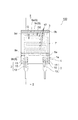
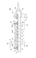
図1は、本発明の好適な実施形態に係る湿度センサ素子100を模式的に示す平面図である。図2は、図1のII−II線に沿った概略断面図である。
(Humidity sensor element)
FIG. 1 is a plan view schematically showing a
図1に示すように、湿度センサ素子100は絶縁基板1を有し、絶縁基板1の一面1a上に一対の櫛形電極3が設けられている。一対の櫛形電極3は、一定のギャップGを介して互いに噛み合うように対向配置されている。各櫛形電極3の端部には端子2が接続されている。一対の櫛形電極3上には、下地膜7が設けられており、この下地膜7上に感湿膜9が設けられている。下地膜7は、感湿膜9を絶縁基板1に強固に固定させ、絶縁基板1からの感湿膜9の剥離を十分に防止するためのものである。下地膜7の膜厚は、0.1μm以下であると好ましい。
As shown in FIG. 1, the
感湿膜9は、一対の櫛形電極3間のギャップ17上に設けられる非盛り上がり部9cと、非盛り上がり部9cに隣接して非盛り上がり部9cの外側に分離して設けられた一対の盛り上がり部9a,9bとを有する。一対の盛り上がり部9a,9bは互いに平行に配置されている。湿度センサ素子100では、感湿膜9のうち、ギャップ17上に設けられた非盛り上がり部9cの抵抗変化が検出される。
The moisture
また、絶縁基板1の一面1a上においては、感湿膜9の一対の盛り上がり部9a,9bの外側に一対の仕切り部5a、5bが分離して配置されている。一対の端子2は、仕切り部5aに対して感湿膜9と反対側に設けられている。すなわち、この仕切り部5aによって、端子2と感湿膜9とが仕切られている。
Further, on the one
以下、湿度センサ素子100のより具体的な構成について説明する。
Hereinafter, a more specific configuration of the
(絶縁基板)
絶縁基板1としては、例えば、ガラス基板、アルミナ基板、石英基板、熱酸化シリコンからなる基板、プラスチック材料を主成分とする基板、水酸基を有する樹脂により被覆された金属基板等を用いることができる。これらのうち、プラスチック材料を主成分とする基板が好ましい。プラスチック材料を主成分とする基板を用いることにより、プラスチック材料以外の材料を主成分とする基板を用いる場合と比べて、湿度センサ素子の軽量化、及び耐衝撃性の向上を図ることができる。このプラスチック材料としては、湿度センサ素子の軽量化及び耐衝撃性の向上を図ることができ且つ耐熱温度が感湿膜9の熱処理温度以上であれば、公知の材料を用いることができ、例えば、ポリイミド、フッ素高分子、フェノール樹脂、エポキシ樹脂等を用いることができる。湿度センサ素子100の感度を高めるためには、このプラスチック材料は、感湿膜9より吸湿性が低いことが好ましい。なお、機械的強度や絶縁特性の安定性を考慮した場合、絶縁基板1としては、アルミナ基板が好ましい。
(Insulated substrate)
As the
(端子)
端子2は、絶縁基板1上に設けられた電極パッド11と、電極パッド11に対して電気的に接続されたリード線13とを有している。電極パッド11は、半田15を介してリード線13と電気的に接続されている。
(Terminal)
The
なお、リード線13は、本体部13aの途中から分岐する挟持部13bを有しており、挟持部13bと本体部13aの先端部13cとによって絶縁基板1の縁及び電極パッド11が挟まれており、これによりリード線13が櫛形電極3に強固に固定されることになる。
The
電極パッド11の構成材料としては、半田との相溶性のある材料が好ましい。かかる材料としては、例えば銅(Cu)、銀(Ag)−パラジウム(Pd)合金、銀(Ag)−白金(Pt)等が挙げられる。より具体的には、電極パッド11は、銀−白金でコーティングされた銅パッドからなる。
The constituent material of the
リード線13の構成材料としては、例えば、リン青銅、銅等が挙げられる。
Examples of the constituent material of the
(櫛形電極)
一対の櫛形電極3は、例えば、金(Au)等の金属や酸化ルテニウム(RuO2)等の金属酸化物等により構成されている。なお、櫛形電極3は、必要に応じて、例えば、ガラスフリットを含有する低抵抗ペーストがスクリーン印刷された後に高温焼結された焼結体により構成される場合もある。特に、下地膜7との密着性を考慮すれば、例えば、櫛形電極3は、表面に水酸基を有する酸化ルテニウムにより構成されているのが好ましい。
(Comb electrode)
The pair of comb-shaped
(仕切り部)
仕切り部5a、5bは、感湿膜9を形成するための感湿膜形成溶液に対して撥液性を有する材料から構成されることが好ましい。感湿膜形成溶液に対して高い撥液性を有する材料としては、フッ素樹脂等が挙げられる。仕切り部5a、5bがフッ素樹脂から形成されていると、フッ素樹脂以外の材料から形成されている場合に比べて、感湿膜9の膜厚を大きくできるとともに、感湿膜9の膜厚の面内バラツキを低減できる。フッ素樹脂としては、例えばポリテトラフルオロエチレン(PTFE)、パーフルオロアルコキシアルカン(PFA)、パーフルオロエチレンプロペンコーポリマー(PFEP)、ポリテトラフルオロエチレン−パーフルオロジオキソールポリマー(TFE/PDD)、ポリビニルフルオライド(PVF)、ポリビニリデンフルオライド(PVDF)又はこれらの誘導体等が挙げられる。
(Partition)
The
(下地膜)
下地膜7は、例えば、シランカップリング剤(シラン化合物)により構成されている。このシランカップリング剤は、例えば、反応性の異なる2種類の官能基としてアルコキシシリル基と不飽和反応性基(例えばエチレン性不飽和反応性基)を含むアクリル系化合物である。より具体的には、3−メタクリロキシプロピルメチルジメトキシシラン、3−メタクリロキシプロピルトリメトキシシラン、3−メタクリロキシプロピルメチルジエトキシシラン、3−メタクリロキシプロピルトリエトキシシラン、3−アクリロキシプロピルトリメトキシシラン、ビニルトリメトキシシラン、ビニルトリエトキシシラン等が挙げられる。
(Undercoat)
The
(感湿膜)
感湿膜9を構成する材料は感湿材料であり、気体中の水分量に応じて抵抗値が変化するものであれば特に制限されず、イオン性重合体(イオン導電性高分子)等が用いられる。感湿膜9を構成する材料として、例えば、感湿材料の架橋物を用いてもよい。感湿材料は、例えば、シランカップリング剤と結合可能なイオン導電性高分子(導電性ポリマー)により構成される。このイオン導電性高分子は、例えば、反応基として不飽和反応性基(例えばエチレン性不飽和反応性基)を含むものであり、具体的には、化1に示したモノマー及び化2に示したモノマーのうちの少なくとも1種以上が共重合された共重合体により構成されている。
(Moisture sensitive film)
The material constituting the moisture-
化1として示したモノマーは、例えば、アミン化合物とジハロゲン化合物とが合成されたものである。アミン化合物としては、例えば、メタクリル酸ジメチルアミノエチルエステルやアクリル酸ジメチルアミノエチルエステル等が挙げられ、ジハロゲン化合物としては、例えば、1,3−ジクロロプロパンや1,3−ジブロモプロパン等が挙げられる。一方、化2として示したモノマーは、例えば、ジアミン化合物とジハロゲン化合物とが合成されて中間体が形成された後、その中間体と所定の化合物とが合成されたものである。ジアミン化合物としては、例えば、N,N,N’,N’−テトラメチル−1,6−ヘキサンジアミン等が挙げられ、ジハロゲン化合物としては、例えば、1,3−ジクロロプロパンや1,12−ジブロモドデカン等が挙げられ、所定の化合物としては、例えば、ジメチルアミノプロピルメタクリルアミド等が挙げられる。
The monomer shown as
ところで、一般に、湿度センサ素子では、感湿膜のうち、一対の電極間のギャップ上に位置する部分における抵抗変化が検出される。したがって、このギャップ上に位置する感湿膜の膜厚のバラツキが大きいと、湿度センサ素子の初期出力のバラツキも大きくなるおそれがあり、盛り上がり部がギャップ上に設けられていると、ギャップ上における感湿膜の膜厚のバラツキが大きくなる。 By the way, in general, in the humidity sensor element, a resistance change is detected in a portion of the moisture sensitive film located on the gap between the pair of electrodes. Therefore, if the variation in the film thickness of the moisture sensitive film located on the gap is large, the variation in the initial output of the humidity sensor element may also be large. If the raised portion is provided on the gap, The variation in the thickness of the moisture sensitive film increases.
本実施形態に係る湿度センサ素子100では、上述したように、ギャップ17上に非盛り上がり部9cが設けられて、その外側に隣接して盛り上がり部9a,9bが設けられている。このため、本実施形態に係る湿度センサ素子100によれば、初期出力のバラツキが低減される。言い換えると、湿度センサ素子100によれば、良好な出力特性が得られる。なお、盛り上がり部9a,9bの最大膜厚と非盛り上がり部9cの最大膜厚との差は、1〜10μmであると好ましい。
In the
また、湿度センサ素子100においては、非盛り上がり部9cの膜厚D1が均一であると好ましい。この場合、より良好な出力特性が得られる。あるいは、電極3上における非盛り上がり部9cの膜厚D1とギャップ17上における非盛り上がり部9cの膜厚D1が同一であると好ましい。
Moreover, in the
また、図2に示すように、湿度センサ素子100では、盛り上がり部9aにおける稜線9dの一面1aへの投影稜線9fからギャップ17までの最短距離D2が50μm以上であると好ましい。この場合、最短距離D2が50μm未満の場合に比べて、より良好な出力特性が得られる。さらに、最短距離D2が100μm以上であるとより好ましい。この場合、最短距離D2が100μm未満の場合に比べて、更に良好な出力特性が得られる。
As shown in FIG. 2, in the
また、湿度センサ素子100では、仕切り部5bから電極3までの最短距離D4は、150μm以上であると好ましい。最短距離D4が150μm以上であると、最短距離D4が150μm未満の場合に比べて湿度センサ素子100の出力特性をより向上できる。この最短距離D4を調整することにより、上記最短距離D2を調整することができる。例えば、最短距離D4を大きくすれば、最短距離D2を大きくすることができる。
In the
同様に、盛り上がり部9bにおける稜線9eの一面1aへの投影稜線9gからギャップ17までの最短距離D3が50μm以上であると好ましい。この場合、最短距離D3が50μm未満の場合に比べて、より良好な出力特性が得られる。さらに、最短距離D3が100μm以上であるとより好ましい。この場合、最短距離D3が100μm未満の場合に比べて、更に良好な出力特性が得られる。
Similarly, it is preferable that the shortest distance D3 from the projected
また、仕切り部5aから電極3までの最短距離D5は、150μm以上であると好ましい。最短距離D5が150μm以上であると、最短距離D5が150μm未満の場合に比べて湿度センサ素子100の出力特性をより向上できる。この最短距離D5を調整することにより、上記最短距離D3を調整することができる。例えば、最短距離D5を大きくすれば、最短距離D3を大きくすることができる。
The shortest distance D5 from the
(湿度センサ素子の製造方法)
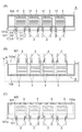
次に、図1、図2、図3(A)〜図3(C)、図4(A)及び図4(B)を参照して、上述した湿度センサ素子100の製造方法について説明する。図3(A)〜図3(C)、図4(A)及び図4(B)は、それぞれ湿度センサ素子100の製造工程を示す概略図である。
(Method for manufacturing humidity sensor element)
Next, a manufacturing method of the
(櫛形電極及び端子形成工程)
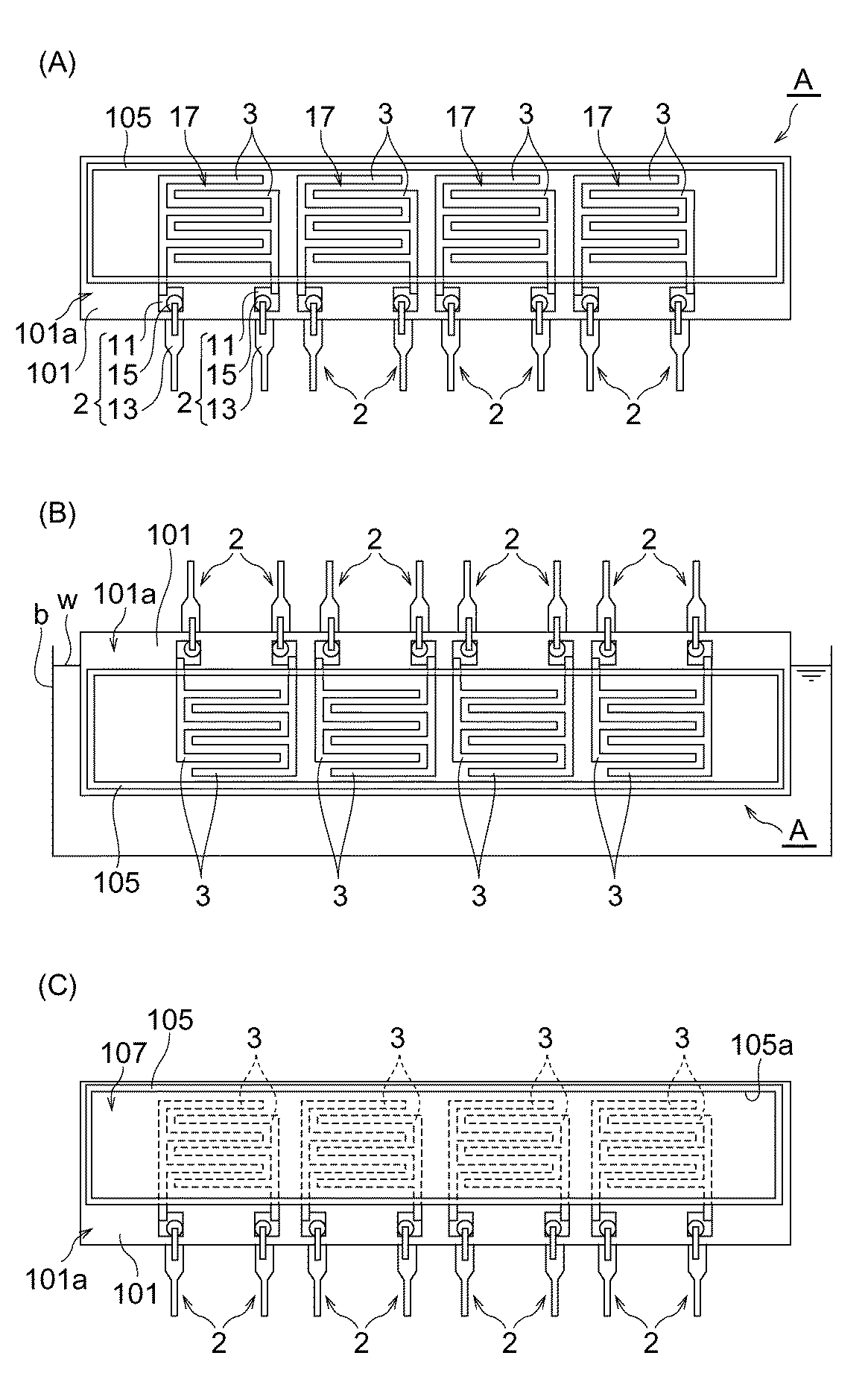
まず、図3(A)に示す構造体Aを準備する。ここで、構造体Aは、絶縁基板101の一面101a上に、一列に配列された複数対の櫛形電極3と、各櫛形電極3に電気的に接続された一対の端子2と、各櫛形電極3によって構成されるギャップ17を取り囲む環状仕切り部105とを備えたものである。
(Comb electrode and terminal formation process)
First, a structure A shown in FIG. Here, the structure A includes a plurality of pairs of
構造体Aを製造するためにはまず絶縁基板101を用意する。絶縁基板101は、必要に応じて公知の方法により洗浄及び乾燥されてもよい。
In order to manufacture the structure A, first, the insulating
続いて、絶縁基板101の一面101a上に、絶縁基板101の縁部に沿って、複数対の電極パッド11を一列に配列して形成する。その後、各対の電極パッド11に対して一対の櫛形電極3を接続する。これにより、複数対の櫛形電極3が、電極パッド11と同様に一列に配列される。ここで、櫛形電極3は、例えば、ガラスフリットを含有する低抵抗ペーストをスクリーン印刷した後に高温焼結して得ることができる。
Subsequently, a plurality of pairs of
続いて、電極パッド11にリード線13を取り付ける。その後、図3(A)に示すように、半田15によりリード線13を電極パッド11に固定する。なお、この後、必要に応じて、例えば半田フラックスを除去するためにリード線13の周辺をアルコール洗浄してもよい。このようにして、櫛形電極3に電気的に接続された端子2が形成される。
Subsequently, the
(仕切り部形成工程)
次に、図3(A)に示されるように、絶縁基板101の一面101a上に環状仕切り部105を形成する。環状仕切り部105は、ギャップ17が内側に配置され複数対の端子2が外側に配置されるようにギャップ17を取り囲む。環状仕切り部105の形成は、例えばディスペンサ法を用いてフッ素樹脂を環状に塗布した後に乾燥させることで行うことができる。ディスペンサ法を用いると、櫛形電極3及びギャップ17上にマスキング材等を塗布する必要がないので、可塑剤等の有機物が櫛形電極3及びギャップ17上に残存することがない。このため、マスキング材等に起因する異物の混入を防止できると共に、かかる異物に起因する感湿膜9の剥離及び湿度センサ素子100の特性劣化を十分に防止できる。こうして構造体Aが得られる。
(Partition formation process)
Next, as illustrated in FIG. 3A, an
(水処理工程)
次に、図3(B)に示されるように、水槽bに収容された水wに、構造体Aを浸漬させる。このとき、複数対の端子2が水wに浸漬しないようにすると好ましい。これにより絶縁基板101の一面101aと水wとが接触する。また構造体Aを水wに浸漬させている間は、必要に応じて超音波をかける。その後、構造体Aを水wから引き上げて乾燥させる。
(Water treatment process)
Next, as shown in FIG. 3B, the structure A is immersed in the water w stored in the water tank b. At this time, it is preferable that the plural pairs of
(下地膜形成工程)
次に、図3(C)に示されるように、絶縁基板101の一面101a上であって環状仕切り部105の内側に下地膜107を形成する。下地膜107は、環状仕切り部105の内側の面105aに接するように形成する。下地膜107は、例えば下地膜形成用溶液を絶縁基板101上に塗布した後に乾燥することで形成することができる。この場合、下地膜107の厚さは環状仕切り部105に近づくにつれて厚くなる傾向にある。下地膜形成用溶液の塗布方法としては、浸漬法等を用いることができる。なお、こうして形成される下地膜107の厚さは、EPMA等を用いて解析することができる。
(Under film forming process)
Next, as illustrated in FIG. 3C, a
下地膜形成用溶液は、上述のシラン化合物を含むと好ましい。この下地膜形成用溶液を用いて下地膜107を形成すると、絶縁基板101と下地膜107との接着性が向上する。
The base film forming solution preferably contains the silane compound described above. When the
(感湿膜形成工程)
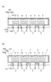
次に、図4(A)に示されるように、下地膜107上であって環状仕切り部105の内側に感湿膜109を形成する。より詳細には、ギャップ17上に非盛り上がり部109cが形成され、非盛り上がり部109cの外周に盛り上がり部109aが形成されるように感湿膜109を形成する。このとき、盛り上がり部109aは、環状仕切り部105の内側に沿って、非盛り上がり部109cを取り囲むように形成される。
(Moisture sensitive film formation process)
Next, as shown in FIG. 4A, a moisture
感湿膜109は、具体的には、感湿膜109を形成するための感湿膜形成溶液を環状仕切り部105の内側の下地膜107上に塗布した後に乾燥することで得ることができる。
Specifically, the moisture
塗布方法としてはディスペンス法が特に好ましい。その他には、例えば浸漬(ディッピング)法、刷毛塗り法、グラビア印刷法、スクリーン印刷法、スピナー塗布法、インクジェット法等種々の方法が使用でき、工程や製品の用途・種類等により選択すればよい。浸漬法は簡便な方法であるが、ディスペンス法に比べて塗布量の制御が困難となる傾向にある。ディスペンス法では、感湿膜形成溶液の滴下量の制御が可能であるので、塗布量の制御も容易である。 As a coating method, a dispensing method is particularly preferable. In addition, various methods such as a dipping method, a brush coating method, a gravure printing method, a screen printing method, a spinner coating method, and an ink jet method can be used, and may be selected depending on the process and the use / type of the product. . The dipping method is a simple method, but it tends to be difficult to control the coating amount as compared with the dispensing method. In the dispensing method, the amount of moisture-sensitive film forming solution dropped can be controlled, so that the amount of coating can be easily controlled.
感湿膜形成溶液は、感湿材料と、これを溶解又は分散させる溶媒とを含む。感湿材料としては、イオン導電性高分子を用い、このイオン導電性高分子としては、例えば化1に示したモノマー及び化2に示したモノマーのうちの少なくとも1種以上が共重合された共重合体であって、化1中のX1−及びX2−又はこれらのいずれか一方が、臭化物イオン又は塩化物イオン等のハロゲン化物イオンであるものを用いると好ましい。
The moisture-sensitive film forming solution contains a moisture-sensitive material and a solvent that dissolves or disperses the moisture-sensitive material. As the moisture sensitive material, an ion conductive polymer is used. As the ion conductive polymer, for example, a copolymer obtained by copolymerizing at least one of the monomer shown in
続いて、感湿膜形成溶液を乾燥させる。その後、感湿膜形成溶液中の感湿材料を必要に応じて架橋処理する。架橋処理は、具体的には、紫外線照射等によって行うことができる。これにより、図4(A)に示すように、下地膜107上に感湿膜109が形成される。
Subsequently, the moisture-sensitive film forming solution is dried. Thereafter, the moisture-sensitive material in the moisture-sensitive film forming solution is subjected to a crosslinking treatment as necessary. Specifically, the crosslinking treatment can be performed by ultraviolet irradiation or the like. As a result, as shown in FIG. 4A, a moisture
このとき、下地膜107がシラン化合物を用いて形成されている場合には、シラン化合物を用いないで下地膜107を形成する場合に比べて、下地膜107と感湿膜109との接着性が向上する。またシラン化合物を用いて下地膜107を形成する場合には、上記水処理工程が行われると、水処理工程を行わない場合に比べて、絶縁基板101とシラン化合物を含む下地膜107との接着性をより十分に向上させることができる。このため、下地膜107の剥離に伴う感湿膜109の剥離を十分に防止できる。また感湿材料が架橋処理されている場合、感湿膜109が気体中の水分によって溶出することが十分に防止される。なお、得られる感湿膜109の高さは通常、環状仕切り部105の高さより低くなる。
At this time, in the case where the
(切断工程)
次に、図4(B)に示されるように、切断線Lに沿って絶縁基板101、下地膜107及び感湿膜109を切断する。この切断線Lは、ギャップ17を挟み且つ環状仕切り部105を横切る線である。例えば、2本の切断線Lに沿って絶縁基板101、下地膜107及び感湿膜109を切断すると、図1及び図2に示される湿度センサ素子100が得られる。このとき、絶縁基板101が絶縁基板1となり、下地膜107が下地膜7となり、感湿膜109が感湿膜9となる。切断は、レーザ光の照射等により行うことができる。切断をより簡便に行うためには、切断線Lの位置における絶縁基板101の裏面に予め溝を形成しておくことが好ましい。なお、切断は、2本の切断線Lに沿って同時に絶縁基板101を切断してもよいし、1本の切断線Lに沿って絶縁基板101を切断した後、もう一方の切断線Lに沿って絶縁基板101を切断するようにしてもよい。
(Cutting process)
Next, as illustrated in FIG. 4B, the insulating
以上の工程を経ることにより、湿度センサ素子100が得られる。
Through the above steps, the
一般に、湿度センサ素子では、感湿膜のうち、一対の電極間のギャップ上に位置する部分における感湿膜の抵抗変化が検出される。したがって、このギャップ上に位置する感湿膜の膜厚のバラツキが大きいと、湿度センサ素子の初期出力のバラツキも大きくなるおそれがある。 In general, the humidity sensor element detects a change in resistance of the moisture sensitive film in a portion of the moisture sensitive film located on the gap between the pair of electrodes. Therefore, if the variation in the film thickness of the moisture sensitive film located on the gap is large, the variation in the initial output of the humidity sensor element may be large.
しかしながら、上記湿度センサ素子100の製造方法によれば、ギャップ17上に、盛り上がり部109aに比べて膜厚にバラツキが生じ難い非盛り上がり部109cを形成し、その外側に隣接して盛り上がり部109aを形成するように感湿膜109を形成する。このため、目的の初期出力を有する湿度センサ素子100、すなわち良好な出力特性を有する湿度センサ素子100が得られる。言い換えると、得られる湿度センサ素子100の初期出力のバラツキを低減できる。
However, according to the manufacturing method of the
また、上記製造方法によれば、感湿膜形成工程において、感湿膜形成溶液の塗布量を変えても良好な出力特性を有する湿度センサ素子100が得られる。この要因としては、感湿膜形成溶液の塗布量を変えると、主として盛り上がり部9a,9bの膜厚が変化し、非盛り上がり部9cの膜厚はほとんど変化しないことが挙げられる。
Further, according to the manufacturing method, the
以上、本発明の好適な実施形態について詳細に説明したが、本発明は上記実施形態に限定されない。 As mentioned above, although preferred embodiment of this invention was described in detail, this invention is not limited to the said embodiment.
例えば、上記湿度センサ素子100において、仕切り部5a,5bを設けないとしてもよい。また、湿度センサ素子100が、仕切り部5a,5bのいずれか一方を有するとしてもよい。いずれの場合であっても、感湿膜は、非盛り上がり部と、その外側に隣接して設けられた盛り上がり部とを有する。このような盛り上がり部は、感湿膜の縁部に形成される。
For example, in the
また、上記湿度センサ素子100において、下地膜7を設けないとしてもよい。さらに、上記湿度センサ素子100では櫛形電極3を用いたが、電極の形状は櫛形に限られない。
In the
また、上記湿度センサ素子100の製造方法において、仕切り部形成工程、水処理工程及び下地膜形成工程のうち1つ以上の工程を省略するとしてもよい。
Moreover, in the manufacturing method of the
以下、実施例及び比較例を用いて本発明を更に詳細に説明するが、本発明は以下の実施例に限定されるものではない。 EXAMPLES Hereinafter, although this invention is demonstrated further in detail using an Example and a comparative example, this invention is not limited to a following example.
(実施例1)
まず、以下の手順を経て感湿膜形成溶液を調製した(特開2003−262600号公報参照)。
(Example 1)
First, a moisture-sensitive film forming solution was prepared through the following procedure (see Japanese Patent Application Laid-Open No. 2003-262600).
N,N,N’,N’−テトラメチルジアミノ−1,12−ドデカン6.30g(36.6mmol)と1,12−ジクロロドデカン9.62g(40.2mmol)を、23gのメタノール中で110℃48時間反応させ、アセトンによる再沈殿で6.04gの白色沈殿を得た。続いて、白色沈殿5.07gとジメチルアミノプロピルメタクリルアミド2.98gをメタノール中90℃で24時間反応させ、アセトン中の逆再沈操作により淡黄色沈殿を2.47g得た。 N, N, N ′, N′-Tetramethyldiamino-1,12-dodecane 6.30 g (36.6 mmol) and 1,12-dichlorododecane 9.62 g (40.2 mmol) were added in 23 g methanol. The mixture was reacted at 48 ° C. for 48 hours, and 6.04 g of a white precipitate was obtained by reprecipitation with acetone. Subsequently, 5.07 g of white precipitate and 2.98 g of dimethylaminopropylmethacrylamide were reacted in methanol at 90 ° C. for 24 hours, and 2.47 g of pale yellow precipitate was obtained by reverse reprecipitation operation in acetone.
この淡黄色沈殿の構成材料の5(質量百分率)エチルセロソルブ溶液を10ml作成し、重合開始剤として0.2%(質量百分率)のKAYACURE ABQ(商品名;日本化薬社製)を添加し、感湿膜形成溶液とした。この感湿膜形成溶液は、4℃で保管された。 10 ml of 5 (mass percentage) ethyl cellosolve solution of the constituent material of this pale yellow precipitate was prepared, and 0.2% (mass percentage) KAYACURE ABQ (trade name; manufactured by Nippon Kayaku Co., Ltd.) was added as a polymerization initiator, A moisture-sensitive film forming solution was obtained. This moisture sensitive film forming solution was stored at 4 ° C.
一方、5mm×8mmの矩形形状を呈する絶縁基板の一面上に、幅150μmの一対の櫛形電極及び電極パッドを形成した。絶縁基板としては、多孔性セラミック基板(商品名:AL100E06PL、ニッコー社製)を用いた。櫛形電極としては、RuO2及びガラスフリットを含む抵抗ペースト(商品名:ex−11、田中貴金属社製)を絶縁基板の一面上にスクリーン印刷によりパターニングした後、高温焼結したものを用いた。この櫛形電極は、絶縁基板の一面上におけるエッジから500μm離れた位置に形成された。電極パッドとしては、導体ペースト(商品名:LF−100、デュポン社製)を絶縁基板の一面上にスクリーン印刷によりパターニングした後、高温焼結したものを用いた。
On the other hand, a pair of comb electrodes and electrode pads having a width of 150 μm were formed on one surface of an insulating substrate having a rectangular shape of 5 mm × 8 mm. As the insulating substrate, a porous ceramic substrate (trade name: AL100E06PL, manufactured by Nikko Corporation) was used. As the comb-shaped electrode, a resistor paste containing RuO 2 and glass frit (trade name: ex-11, manufactured by Tanaka Kikinzoku Co., Ltd.) was patterned on one surface of an insulating substrate by screen printing, and then sintered at a high temperature. The comb electrode was formed at a
続いて、半田を用いて電極パッドにリード線を取り付けた。続いて、半田フラックスを除去するために、100mlのイソプロピルアルコール中に超音波をかけながら10分間にわたって絶縁基板を浸漬させて洗浄した後、放置して乾燥させた。 Subsequently, lead wires were attached to the electrode pads using solder. Subsequently, in order to remove the solder flux, the insulating substrate was immersed and washed in 100 ml of isopropyl alcohol for 10 minutes while applying ultrasonic waves, and then left to dry.
次に、日本レーザ電子製のUVオゾンクリーナーNL−UV252を用いて、4.5W×2の条件で10分間、絶縁基板の一面に対してUVオゾン処理を行った。 Next, UV ozone treatment was performed on one surface of the insulating substrate for 10 minutes under the condition of 4.5 W × 2 using a UV ozone cleaner NL-UV252 manufactured by Nippon Laser Electronics.
他方、環状仕切り部を形成するために、環状仕切り部形成用溶液を調整した。環状仕切り部形成用溶液は、ポリテトラフルオロエチレン(商品名:テフロンAF、三井・デュポンフロロケミカル社製)とフッ素系不活性液体(商品名:フロリナートFC−75、住友スリーエム社製)とで構成した。 On the other hand, an annular partition portion forming solution was prepared in order to form an annular partition portion. The solution for forming the annular partition portion is composed of polytetrafluoroethylene (trade name: Teflon AF, manufactured by Mitsui DuPont Fluorochemical Co., Ltd.) and a fluorine-based inert liquid (trade name: Fluorinert FC-75, manufactured by Sumitomo 3M Co.). did.
そして、ディスペンサ法を用いて、一対の櫛形電極間に形成されたギャップを取り囲むようにポリテトラフルオロエチレンを含む環状仕切り部形成溶液を絶縁基板上に塗布した後、乾燥させた。このようにして、ポリテトラフルオロエチレンからなる幅250μmの環状仕切り部を形成した。このとき、ギャップが環状仕切り部の内側に配置され、電極パッドが環状仕切り部の外側に配置されるようにした。 Then, using a dispenser method, an annular partition portion forming solution containing polytetrafluoroethylene was applied on the insulating substrate so as to surround the gap formed between the pair of comb electrodes, and then dried. In this way, an annular partition portion having a width of 250 μm made of polytetrafluoroethylene was formed. At this time, the gap was arranged inside the annular partition part, and the electrode pad was arranged outside the annular partition part.
こうして、絶縁基板上に電極パッド及び櫛形電極が形成された構造体を得た。続いて、この構造体を、超音波をかけながら10分間にわたって蒸留水中に浸漬させた後、自然乾燥させた。 Thus, a structure having electrode pads and comb-shaped electrodes formed on an insulating substrate was obtained. Subsequently, the structure was immersed in distilled water for 10 minutes while applying ultrasonic waves, and then naturally dried.
続いて、シランカップリング剤として3−メタクリロキシプロピルトリメトキシシラン(信越化学製KBM−503)を使用し、その1%(質量百分率)酢酸水溶液で絶縁基板を処理して乾燥させた後、120℃で20分間にわたって放置し、絶縁基板の表面にアクリロイル基を導入するようにした。こうして、シランカップリング剤を塗膜化して下地膜を形成した。 Subsequently, 3-methacryloxypropyltrimethoxysilane (KBM-503 manufactured by Shin-Etsu Chemical Co., Ltd.) was used as the silane coupling agent, and the insulating substrate was treated with 1% (mass percentage) acetic acid aqueous solution and dried. The mixture was allowed to stand at 20 ° C. for 20 minutes to introduce acryloyl groups on the surface of the insulating substrate. Thus, a silane coupling agent was formed into a coating film to form a base film.
続いて、ディスペンサ法を用いて、各ギャップ上に上記感湿膜形成溶液をそれぞれ滴下した後、25℃で15分間にわたって乾燥させることにより、感湿膜形成溶液を塗膜化した。このとき、感湿膜形成溶液の滴下量を2.5μlとした。 Subsequently, the moisture sensitive film forming solution was dropped onto each gap by using a dispenser method, and then dried at 25 ° C. for 15 minutes to form a moisture sensitive film forming solution. At this time, the dropping amount of the moisture sensitive film forming solution was 2.5 μl.
次に、窒素雰囲気中で塗膜に1分間にわたって紫外線を照射して重合させることにより、環状仕切り部の内側に膜厚5μmの感湿膜を形成した。この際、紫外線照射量を1000mJ/cm2とした。 Next, the coating film was irradiated with ultraviolet rays for 1 minute in a nitrogen atmosphere and polymerized to form a moisture sensitive film having a thickness of 5 μm inside the annular partition. At this time, the ultraviolet irradiation amount was set to 1000 mJ / cm 2 .
そして、各ギャップを分離するように絶縁基板を切断して、図1及び図2に示されるような湿度センサ素子を得た。この湿度センサ素子について、次のようにして盛り上がり部を確認した。 And the insulating substrate was cut | disconnected so that each gap might be isolate | separated, and the humidity sensor element as shown in FIG.1 and FIG.2 was obtained. About this humidity sensor element, the rising part was confirmed as follows.
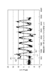
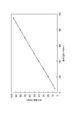
すなわち、本実施例の湿度センサ素子について、レーザーフォーカス変位計LT−8010−COM2を用いて、絶縁基板の一面からの変位量(高さ)を測定した。その結果を図5に示す。図5は、横軸を絶縁基板の一面に沿ったエッジからの距離(μm)、縦軸を絶縁基板の一面に垂直な方向の変位量(μm)とした場合のグラフである。図5において、チャートL1は感湿膜が設けられていない状態(リファレンス)を示し、チャートL2は感湿膜が設けられている状態を示す。すなわち、チャートL1は、絶縁基板の一面及び櫛形電極の表面のプロファイルを描いたものであり、チャートL2は、絶縁基板の一面及び櫛形電極の表面上に感湿膜を形成した場合の感湿膜表面のプロファイルを描いたものである。これらのチャートL1,L2の差分を取ると、絶縁基板のエッジから500〜600μm程度離れた場所に、感湿膜の盛り上がり部P1が確認された。一方、盛り上がり部P1に最も近いギャップR1までの距離はおよそ800μmであった。このことから、図5に示されるように、ギャップR1上には盛り上がり部P1が形成されていないことが確認された。 That is, with respect to the humidity sensor element of this example, the displacement amount (height) from one surface of the insulating substrate was measured using a laser focus displacement meter LT-8010-COM2. The result is shown in FIG. FIG. 5 is a graph when the horizontal axis is the distance (μm) from the edge along one surface of the insulating substrate, and the vertical axis is the displacement (μm) in the direction perpendicular to the one surface of the insulating substrate. In FIG. 5, chart L1 shows a state (reference) in which no moisture sensitive film is provided, and chart L2 shows a state in which a moisture sensitive film is provided. That is, the chart L1 depicts a profile of one surface of the insulating substrate and the surface of the comb-shaped electrode, and the chart L2 represents a moisture-sensitive film when a moisture-sensitive film is formed on one surface of the insulating substrate and the surface of the comb-shaped electrode. A profile of the surface. When the difference between these charts L1 and L2 was taken, a raised portion P1 of the moisture sensitive film was confirmed at a location about 500 to 600 μm away from the edge of the insulating substrate. On the other hand, the distance to the gap R1 closest to the raised portion P1 was about 800 μm. From this, it was confirmed that the raised portion P1 was not formed on the gap R1, as shown in FIG.
なお、本実施例の湿度センサ素子については、図2における最短距離D4は150μm、最短距離D5が150μmであった。 In addition, about the humidity sensor element of a present Example, the shortest distance D4 in FIG. 2 was 150 micrometers, and the shortest distance D5 was 150 micrometers.
(実施例2)
最短距離D4が200μm、最短距離D5が200μmとなるように仕切り部及び櫛形電極を配置したこと以外は実施例1と同様にして湿度センサ素子を得た。
(Example 2)
A humidity sensor element was obtained in the same manner as in Example 1 except that the partition portion and the comb electrode were arranged so that the shortest distance D4 was 200 μm and the shortest distance D5 was 200 μm.
この湿度センサ素子の盛り上がり部の位置を実施例1と同様にして確認した。その結果、実施例1と同様、ギャップR1上には盛り上がり部P1が形成されていないことが確認された。 The position of the raised portion of the humidity sensor element was confirmed in the same manner as in Example 1. As a result, as in Example 1, it was confirmed that the raised portion P1 was not formed on the gap R1.
(比較例1)
最短距離D4が100μm、最短距離D5が100μmとなるように仕切り部及び櫛形電極を配置したこと以外は実施例1と同様にして湿度センサ素子を得た。
(Comparative Example 1)
A humidity sensor element was obtained in the same manner as in Example 1 except that the partition portion and the comb electrode were arranged so that the shortest distance D4 was 100 μm and the shortest distance D5 was 100 μm.
この湿度センサ素子の盛り上がり部の位置を実施例1と同様にして確認した。その結果、ギャップR1上に盛り上がり部P1が形成されていることが確認された。 The position of the raised portion of the humidity sensor element was confirmed in the same manner as in Example 1. As a result, it was confirmed that the raised portion P1 was formed on the gap R1.
(比較例2)
最短距離D4が120μm、最短距離D5が120μmとなるように仕切り部及び櫛形電極を配置したこと以外は実施例1と同様にして湿度センサ素子を得た。
(Comparative Example 2)
A humidity sensor element was obtained in the same manner as in Example 1 except that the partition portion and the comb-shaped electrode were arranged so that the shortest distance D4 was 120 μm and the shortest distance D5 was 120 μm.
この湿度センサ素子の盛り上がり部の位置を実施例1と同様にして確認した。その結果、ギャップR1上に盛り上がり部P1が形成されていることが確認された。 The position of the raised portion of the humidity sensor element was confirmed in the same manner as in Example 1. As a result, it was confirmed that the raised portion P1 was formed on the gap R1.
(比較例3)
最短距離D4が80μm、最短距離D5が150μmとなるように仕切り部及び櫛形電極を配置したこと以外は実施例1と同様にして湿度センサ素子を得た。
(Comparative Example 3)
A humidity sensor element was obtained in the same manner as in Example 1 except that the partition portion and the comb electrode were arranged so that the shortest distance D4 was 80 μm and the shortest distance D5 was 150 μm.
この湿度センサ素子の盛り上がり部の位置を、実施例1と同様にして確認した。その結果、ギャップR1上に盛り上がり部P1が形成されていることが確認された。 The position of the raised portion of the humidity sensor element was confirmed in the same manner as in Example 1. As a result, it was confirmed that the raised portion P1 was formed on the gap R1.
(実施例3〜18)
感湿膜溶液の滴下量、最短距離D4及び最短距離D5を表1及び表2に示される値としたこと以外は実施例1と同様にして湿度センサ素子を得た。これらの湿度センサ素子の盛り上がり部の位置を実施例1と同様にして確認した。その結果、実施例1と同様、ギャップR1上には盛り上がり部P1が形成されていないことが確認された。
(Examples 3 to 18)
A humidity sensor element was obtained in the same manner as in Example 1 except that the dripping amount of the moisture sensitive film solution, the shortest distance D4, and the shortest distance D5 were set to the values shown in Tables 1 and 2. The positions of the raised portions of these humidity sensor elements were confirmed in the same manner as in Example 1. As a result, as in Example 1, it was confirmed that the raised portion P1 was not formed on the gap R1.
(比較例4〜27)
感湿膜溶液の滴下量、最短距離D4及び最短距離D5を表1及び表2に示される値としたこと以外は実施例1と同様にして湿度センサ素子を得た。これらの湿度センサ素子の盛り上がり部の位置を、実施例1と同様にして確認した。その結果、ギャップR1上に盛り上がり部P1が形成されていることが確認された。
(Comparative Examples 4-27)
A humidity sensor element was obtained in the same manner as in Example 1 except that the dripping amount of the moisture sensitive film solution, the shortest distance D4, and the shortest distance D5 were set to the values shown in Tables 1 and 2. The positions of the raised portions of these humidity sensor elements were confirmed in the same manner as in Example 1. As a result, it was confirmed that the raised portion P1 was formed on the gap R1.
(出力特性評価)
上記実施例1〜18及び比較例1〜27の湿度センサ素子について耐水性試験を行い、これらの出力特性を評価した。
(Output characteristic evaluation)
A water resistance test was performed on the humidity sensor elements of Examples 1 to 18 and Comparative Examples 1 to 27, and their output characteristics were evaluated.
耐水性試験は、以下の手順で行われた。すなわち、まず、湿度変化を周波数変化に変換する湿度−周波数変換回路(特開平3−28751号公報参照)に湿度センサ素子を組み込んだ後、分流式湿度発生装置モデルSRH−1(商品名、神栄株式会社製)を使用して、湿度センサ素子の出力電圧を測定した。 The water resistance test was performed according to the following procedure. That is, first, a humidity sensor element is incorporated into a humidity-frequency conversion circuit (see Japanese Patent Laid-Open No. 3-28751) that converts a humidity change into a frequency change, and then a shunt-type humidity generator model SRH-1 (trade name, Shinei) Was used to measure the output voltage of the humidity sensor element.
まず、25℃、5%RHの相対湿度下に湿度センサ素子を30分間放置して出力電圧を測定した。その後、相対湿度を95%RHまで上昇させた。このとき、10%RH、20%RH、30%RH、40%RH、50%RH、60%RH、70%RH、80%RH、90%RH、95%RHの各湿度条件において、湿度センサ素子を30分間放置してそれぞれ出力電圧を測定した。 First, the humidity sensor element was left for 30 minutes at 25 ° C. and 5% RH relative humidity, and the output voltage was measured. Thereafter, the relative humidity was increased to 95% RH. At this time, humidity sensor in each humidity condition of 10% RH, 20% RH, 30% RH, 40% RH, 50% RH, 60% RH, 70% RH, 80% RH, 90% RH, 95% RH The device was left for 30 minutes and the output voltage was measured.
次に、相対湿度を5%RHまで下降させた。このとき、90%RH、80%RH、70%RH、60%RH、50%RH、40%RH、30%RH、20%RH、10%RH、5%RHの各湿度条件において、湿度センサ素子を30分間放置してそれぞれ出力電圧を測定した。 Next, the relative humidity was lowered to 5% RH. At this time, the humidity sensor in each humidity condition of 90% RH, 80% RH, 70% RH, 60% RH, 50% RH, 40% RH, 30% RH, 20% RH, 10% RH, 5% RH The device was left for 30 minutes and the output voltage was measured.
そして、上昇過程での各湿度条件における出力電圧値と、下降過程での各湿度条件における出力電圧値との平均値を、当該湿度条件における出力電圧値とした。さらに、この出力電圧値から湿度センサ素子が表示する出力湿度を算出した。 And the average value of the output voltage value in each humidity condition in an ascending process and the output voltage value in each humidity condition in a descending process was made into the output voltage value in the said humidity condition. Further, the output humidity displayed by the humidity sensor element was calculated from the output voltage value.
図6は、設定湿度に対する実施例1の湿度センサ素子の出力湿度を示すグラフである。このグラフから、5〜95%RHの範囲内において実施例1の湿度センサ素子が良好な出力特性を有していることが確認された。同様に、実施例2〜18及び比較例1〜27の湿度センサ素子についても出力特性の評価を行ったところ、実施例2〜18の湿度センサ素子は、実施例1の湿度センサ素子と同様、比較例1〜27の湿度センサ素子に比べて、より良好な出力特性を有していることが分かった。 FIG. 6 is a graph showing the output humidity of the humidity sensor element of Example 1 with respect to the set humidity. From this graph, it was confirmed that the humidity sensor element of Example 1 had good output characteristics within the range of 5 to 95% RH. Similarly, when the output characteristics of the humidity sensor elements of Examples 2 to 18 and Comparative Examples 1 to 27 were evaluated, the humidity sensor elements of Examples 2 to 18 were the same as the humidity sensor elements of Example 1. It turned out that it has a more favorable output characteristic compared with the humidity sensor element of Comparative Examples 1-27.
(初期出力のバラツキ評価)
実施例1〜18及び比較例1〜27の湿度センサ素子を、それぞれ80個ずつ作製した。続いて、各々の湿度センサ素子について、設定湿度50%RHにおける初期出力(作製直後の出力湿度)を測定した。
(Evaluation of initial output variation)
80 humidity sensor elements of Examples 1 to 18 and Comparative Examples 1 to 27 were produced. Subsequently, for each humidity sensor element, an initial output (output humidity immediately after fabrication) at a set humidity of 50% RH was measured.
表1及び表2に示されるように、滴下量が同一の場合を比較すると、実施例1〜18における湿度センサ素子の歩留まりは、比較例1〜27における湿度センサ素子の歩留まりよりも高かった。これは、実施例の湿度センサ素子では、比較例の湿度センサ素子に比べて初期出力のバラツキが小さいことに起因している。例えば、実施例1,2の湿度センサ素子では初期出力のバラツキが小さいので、出力湿度が49〜51%RHの湿度センサ素子が98.8%の歩留まりで得られた。これに対して、比較例1〜3の湿度センサ素子では92.5〜95%の歩留まりしか得られなかった。 As shown in Tables 1 and 2, when the amount of dripping was the same, the yield of the humidity sensor elements in Examples 1 to 18 was higher than the yield of the humidity sensor elements in Comparative Examples 1 to 27. This is due to the fact that the variation in the initial output is smaller in the humidity sensor element of the embodiment than in the humidity sensor element of the comparative example. For example, the humidity sensor elements of Examples 1 and 2 have a small initial output variation, so that a humidity sensor element having an output humidity of 49 to 51% RH was obtained with a yield of 98.8%. On the other hand, in the humidity sensor elements of Comparative Examples 1 to 3, only a yield of 92.5 to 95% was obtained.
以上の結果から、本発明による湿度センサ素子の製造方法によれば、湿度センサ素子の初期出力のバラツキを低減できることが確認された。また、本発明による湿度センサ素子によれば、より良好な出力特性が得られることが確認された。 From the above results, it was confirmed that the variation in the initial output of the humidity sensor element can be reduced according to the method for manufacturing the humidity sensor element of the present invention. Further, it was confirmed that the humidity sensor element according to the present invention can obtain better output characteristics.
1…絶縁基板、1a…絶縁基板一面、3…一対の電極、9…感湿膜、100…湿度センサ素子、17…一対の電極間のギャップ、9c…非盛り上がり部、9a,9b…盛り上がり部、D1…非盛り上がり部の膜厚、9d,9e…盛り上がり部の稜線、9f,9g…投影稜線。
DESCRIPTION OF
Claims (4)
前記感湿膜形成工程において、前記一対の電極間のギャップ上に非盛り上がり部が形成され、前記非盛り上がり部の外側に前記非盛り上がり部に隣接して盛り上がり部が形成されるように前記感湿膜を形成することを特徴とする湿度センサ素子の製造方法。 A humidity sensor element manufacturing method including a moisture sensitive film forming step of forming a moisture sensitive film on a pair of electrodes formed on one surface of an insulating substrate so as to face each other,
In the moisture sensitive film forming step, the moisture sensitive part is formed on the gap between the pair of electrodes, and the raised part is formed outside the non-swelled part and adjacent to the non-swelled part. A method of manufacturing a humidity sensor element, comprising forming a film.
前記感湿膜が、前記一対の電極間のギャップ上に設けられる非盛り上がり部と、前記非盛り上がり部の外側に前記非盛り上がり部に隣接して設けられる盛り上がり部と、を有することを特徴とする湿度センサ素子。 A humidity sensor element comprising a pair of electrodes provided on one surface of an insulating substrate so as to face each other, and a moisture sensitive film provided on the pair of electrodes,
The moisture-sensitive film has a non-swelled part provided on the gap between the pair of electrodes, and a swelled part provided on the outside of the non-swelled part adjacent to the non-swelled part. Humidity sensor element.
Priority Applications (1)
| Application Number | Priority Date | Filing Date | Title |
|---|---|---|---|
| JP2004106683A JP2005291886A (en) | 2004-03-31 | 2004-03-31 | Manufacturing method of humidity sensor element, and the humidity sensor element |
Applications Claiming Priority (1)
| Application Number | Priority Date | Filing Date | Title |
|---|---|---|---|
| JP2004106683A JP2005291886A (en) | 2004-03-31 | 2004-03-31 | Manufacturing method of humidity sensor element, and the humidity sensor element |
Publications (1)
| Publication Number | Publication Date |
|---|---|
| JP2005291886A true JP2005291886A (en) | 2005-10-20 |
Family
ID=35324977
Family Applications (1)
| Application Number | Title | Priority Date | Filing Date |
|---|---|---|---|
| JP2004106683A Withdrawn JP2005291886A (en) | 2004-03-31 | 2004-03-31 | Manufacturing method of humidity sensor element, and the humidity sensor element |
Country Status (1)
| Country | Link |
|---|---|
| JP (1) | JP2005291886A (en) |
Cited By (7)
| Publication number | Priority date | Publication date | Assignee | Title |
|---|---|---|---|---|
| JP2007322184A (en) * | 2006-05-31 | 2007-12-13 | Ngk Spark Plug Co Ltd | Ammonia gas sensor |
| JP2008107166A (en) * | 2006-10-24 | 2008-05-08 | Denso Corp | Humidity sensor and manufacturing method thereof |
| WO2008126897A1 (en) * | 2007-04-10 | 2008-10-23 | Hokuriku Electric Industry Co., Ltd. | Sensing sensor and manufacturing method of the same |
| WO2012169148A1 (en) * | 2011-06-06 | 2012-12-13 | 株式会社デンソー | Humidity sensor and method for manufacturing same |
| JP2017106886A (en) * | 2015-12-11 | 2017-06-15 | 台湾ナノカーボンテクノロジー股▲ふん▼有限公司Taiwan Carbon Nano Technology Corporation | Gas sensor and manufacturing method thereof |
| JP2017104487A (en) * | 2015-12-11 | 2017-06-15 | 台湾ナノカーボンテクノロジー股▲ふん▼有限公司Taiwan Carbon Nano Technology Corporation | Ventilator using gas identification and having pneumonia infection and pneumoniae species disease analysis function |
| JP2022084164A (en) * | 2020-11-26 | 2022-06-07 | 日本特殊陶業株式会社 | Gas sensor |
-
2004
- 2004-03-31 JP JP2004106683A patent/JP2005291886A/en not_active Withdrawn
Cited By (9)
| Publication number | Priority date | Publication date | Assignee | Title |
|---|---|---|---|---|
| JP2007322184A (en) * | 2006-05-31 | 2007-12-13 | Ngk Spark Plug Co Ltd | Ammonia gas sensor |
| JP2008107166A (en) * | 2006-10-24 | 2008-05-08 | Denso Corp | Humidity sensor and manufacturing method thereof |
| WO2008126897A1 (en) * | 2007-04-10 | 2008-10-23 | Hokuriku Electric Industry Co., Ltd. | Sensing sensor and manufacturing method of the same |
| WO2012169148A1 (en) * | 2011-06-06 | 2012-12-13 | 株式会社デンソー | Humidity sensor and method for manufacturing same |
| US9239309B2 (en) | 2011-06-06 | 2016-01-19 | Denso Corporation | Humidity sensor and method of manufacturing the same |
| JP2017106886A (en) * | 2015-12-11 | 2017-06-15 | 台湾ナノカーボンテクノロジー股▲ふん▼有限公司Taiwan Carbon Nano Technology Corporation | Gas sensor and manufacturing method thereof |
| JP2017104487A (en) * | 2015-12-11 | 2017-06-15 | 台湾ナノカーボンテクノロジー股▲ふん▼有限公司Taiwan Carbon Nano Technology Corporation | Ventilator using gas identification and having pneumonia infection and pneumoniae species disease analysis function |
| JP2022084164A (en) * | 2020-11-26 | 2022-06-07 | 日本特殊陶業株式会社 | Gas sensor |
| JP7453129B2 (en) | 2020-11-26 | 2024-03-19 | 日本特殊陶業株式会社 | gas sensor |
Similar Documents
| Publication | Publication Date | Title |
|---|---|---|
| CN109932402B (en) | Hot wire type gas sensor chip, sensor and preparation method of sensor | |
| JP4746009B2 (en) | Thin film transistor having poly (arylene ether) polymer as gate dielectric layer and passivation layer | |
| TW509791B (en) | Humidity sensor element and method for manufacture the same | |
| JP2005291886A (en) | Manufacturing method of humidity sensor element, and the humidity sensor element | |
| JP2011507457A (en) | Composite passive materials for ultrasonic transducers | |
| US20160370336A1 (en) | Micro Heater and Micro Sensor | |
| US5866800A (en) | Gas sensor and method for fabricating same | |
| JP2008509439A5 (en) | ||
| CN113129776A (en) | Anti-oxidation transparent display film and manufacturing method thereof | |
| JP2023053065A (en) | Oxygen electrode, measuring device, and method for manufacturing oxygen electrode | |
| US20200033285A1 (en) | Humidity sensor | |
| WO1993016377A1 (en) | Humidity sensor and its manufacture | |
| JP2005283482A (en) | Manufacturing method of humidity sensor element | |
| JP2018056247A (en) | Electronic component housing package, electronic device and manufacturing method of electronic component housing package | |
| JP5454839B2 (en) | Antifuse element | |
| WO2018165841A1 (en) | Ultrathin electrochemical gas sensor | |
| JP4236021B2 (en) | Electronic component having humidity detection function and manufacturing method thereof | |
| CN1493080A (en) | Metal resistor device and method of manufacturing the same | |
| KR100289570B1 (en) | Connecting Actuator and Power Supply Line Using Auxiliary Electrode | |
| CN100382203C (en) | Manufacturing method of thin film resistors | |
| JP3571299B2 (en) | Humidity sensor and method of manufacturing humidity sensor | |
| JP5262159B2 (en) | Method for manufacturing thin film chip resistor | |
| CN212624003U (en) | Sensing structure, light-emitting module and electronic equipment | |
| JPH0781975B2 (en) | Moisture sensitive element | |
| JP2005291880A (en) | Humidity sensor element |
Legal Events
| Date | Code | Title | Description |
|---|---|---|---|
| A300 | Withdrawal of application because of no request for examination |
Free format text: JAPANESE INTERMEDIATE CODE: A300 Effective date: 20070605 |