JP2005291839A - Projection device and three-dimensional shape detection device - Google Patents
Projection device and three-dimensional shape detection device Download PDFInfo
- Publication number
- JP2005291839A JP2005291839A JP2004105427A JP2004105427A JP2005291839A JP 2005291839 A JP2005291839 A JP 2005291839A JP 2004105427 A JP2004105427 A JP 2004105427A JP 2004105427 A JP2004105427 A JP 2004105427A JP 2005291839 A JP2005291839 A JP 2005291839A
- Authority
- JP
- Japan
- Prior art keywords
- projection
- light emitting
- image
- semiconductor light
- lens
- Prior art date
- Legal status (The legal status is an assumption and is not a legal conclusion. Google has not performed a legal analysis and makes no representation as to the accuracy of the status listed.)
- Granted
Links
Images


Classifications
-
- H—ELECTRICITY
- H04—ELECTRIC COMMUNICATION TECHNIQUE
- H04N—PICTORIAL COMMUNICATION, e.g. TELEVISION
- H04N9/00—Details of colour television systems
- H04N9/12—Picture reproducers
- H04N9/31—Projection devices for colour picture display, e.g. using electronic spatial light modulators [ESLM]
- H04N9/3141—Constructional details thereof
- H04N9/317—Convergence or focusing systems
-
- F—MECHANICAL ENGINEERING; LIGHTING; HEATING; WEAPONS; BLASTING
- F21—LIGHTING
- F21K—NON-ELECTRIC LIGHT SOURCES USING LUMINESCENCE; LIGHT SOURCES USING ELECTROCHEMILUMINESCENCE; LIGHT SOURCES USING CHARGES OF COMBUSTIBLE MATERIAL; LIGHT SOURCES USING SEMICONDUCTOR DEVICES AS LIGHT-GENERATING ELEMENTS; LIGHT SOURCES NOT OTHERWISE PROVIDED FOR
- F21K9/00—Light sources using semiconductor devices as light-generating elements, e.g. using light-emitting diodes [LED] or lasers
-
- G—PHYSICS
- G01—MEASURING; TESTING
- G01B—MEASURING LENGTH, THICKNESS OR SIMILAR LINEAR DIMENSIONS; MEASURING ANGLES; MEASURING AREAS; MEASURING IRREGULARITIES OF SURFACES OR CONTOURS
- G01B11/00—Measuring arrangements characterised by the use of optical techniques
- G01B11/24—Measuring arrangements characterised by the use of optical techniques for measuring contours or curvatures
- G01B11/25—Measuring arrangements characterised by the use of optical techniques for measuring contours or curvatures by projecting a pattern, e.g. one or more lines, moiré fringes on the object
-
- G—PHYSICS
- G03—PHOTOGRAPHY; CINEMATOGRAPHY; ANALOGOUS TECHNIQUES USING WAVES OTHER THAN OPTICAL WAVES; ELECTROGRAPHY; HOLOGRAPHY
- G03B—APPARATUS OR ARRANGEMENTS FOR TAKING PHOTOGRAPHS OR FOR PROJECTING OR VIEWING THEM; APPARATUS OR ARRANGEMENTS EMPLOYING ANALOGOUS TECHNIQUES USING WAVES OTHER THAN OPTICAL WAVES; ACCESSORIES THEREFOR
- G03B21/00—Projectors or projection-type viewers; Accessories therefor
- G03B21/005—Projectors using an electronic spatial light modulator but not peculiar thereto
- G03B21/006—Projectors using an electronic spatial light modulator but not peculiar thereto using LCD's
-
- G—PHYSICS
- G06—COMPUTING OR CALCULATING; COUNTING
- G06T—IMAGE DATA PROCESSING OR GENERATION, IN GENERAL
- G06T7/00—Image analysis
- G06T7/50—Depth or shape recovery
- G06T7/521—Depth or shape recovery from laser ranging, e.g. using interferometry; from the projection of structured light
-
- H—ELECTRICITY
- H04—ELECTRIC COMMUNICATION TECHNIQUE
- H04N—PICTORIAL COMMUNICATION, e.g. TELEVISION
- H04N5/00—Details of television systems
- H04N5/74—Projection arrangements for image reproduction, e.g. using eidophor
- H04N5/7416—Projection arrangements for image reproduction, e.g. using eidophor involving the use of a spatial light modulator, e.g. a light valve, controlled by a video signal
Landscapes
- Engineering & Computer Science (AREA)
- Physics & Mathematics (AREA)
- General Physics & Mathematics (AREA)
- Signal Processing (AREA)
- Computer Vision & Pattern Recognition (AREA)
- Multimedia (AREA)
- Optics & Photonics (AREA)
- Theoretical Computer Science (AREA)
- Microelectronics & Electronic Packaging (AREA)
- General Engineering & Computer Science (AREA)
- Length Measuring Devices By Optical Means (AREA)
- Projection Apparatus (AREA)
- Led Device Packages (AREA)
Abstract
【課題】 半導体発光素子から空間変調素子に照射される光の照度ムラを抑制し、投影面に高品質の画像を投影することができる投影装置および3次元形状検出装置を提供すること。
【解決手段】 複数のLED17は基板上16に千鳥状に配列され、1のLED17と、その1のLED17のまわりのLED17との間隔dは、LED17の1つから出射された光によって投影LCD19において形成される照度分布が半値全幅以下になるように設定されている。よって、投影LCD19に略均一に光を照射することができ、投影LCD19における照度ムラは抑制され、投影面に高品質の画像を投影することができる。
【選択図】 図4
PROBLEM TO BE SOLVED: To provide a projection device and a three-dimensional shape detection device capable of suppressing illuminance unevenness of light irradiated from a semiconductor light emitting element to a spatial modulation element and projecting a high quality image on a projection surface.
A plurality of LEDs 17 are arranged in a zigzag pattern on a substrate 16, and a distance d between one LED 17 and the LEDs 17 around the one LED 17 is determined in the projection LCD 19 by light emitted from one of the LEDs 17. The illuminance distribution to be formed is set to be equal to or less than the full width at half maximum. Therefore, it is possible to irradiate the projection LCD 19 with light substantially uniformly, and uneven illuminance in the projection LCD 19 is suppressed, and a high-quality image can be projected onto the projection surface.
[Selection] Figure 4
Description
本発明は、半導体発光素子から空間変調素子に照射される光の照度ムラを抑制し、投影面に高品質の画像を投影することができる投影装置および3次元形状検出装置に関する。 The present invention relates to a projection apparatus and a three-dimensional shape detection apparatus that can suppress unevenness in illuminance of light irradiated from a semiconductor light emitting element to a spatial modulation element and project a high-quality image on a projection surface.
従来より、光源から出射される光を集光光学系によって集光し、その集光された光に空間変調素子によって画像信号に応じた空間変調が施して、その空間変調を施した光を画像信号光として投影手段を介して投影面に投影することで、任意の画像を投影面に投影する投影装置が知られている。 Conventionally, light emitted from a light source is condensed by a condensing optical system, and the collected light is subjected to spatial modulation according to an image signal by a spatial modulation element, and the spatially modulated light is imaged. A projection apparatus that projects an arbitrary image on a projection surface by projecting it as signal light onto a projection surface via a projection means is known.
しかし、この投影装置の光源としては、従来、キセノンランプ、ハロゲンランプ、メタルハライドランプ等が使用されていたため、光源としての寿命が短い上オンオフ変調ができないので連続点灯することを余儀なくされ、消費電力が大きいという問題点があった。 However, since a xenon lamp, a halogen lamp, a metal halide lamp or the like has been conventionally used as the light source of this projection apparatus, it has a short life as a light source and cannot be turned on / off, so it must be lit continuously and consumes power. There was a problem of being big.
そこで、この問題を解決すべく、次の特許文献1や特許文献2には投影装置の光源として半導体発光素子、具体的には、発光ダイオード(以下「LED」と称す)を用いる技術が開示されている。
In order to solve this problem, the following
投影装置の光源としてLEDを用いることにより、光源の長寿命化、低消費電力化を図ることができることに加え、LEDの出力光は、指向性が強く、発光面積も小さいため、集光効率が高まり、結果的に光利用効率を向上させることができる。
しかしながら、上述した投影装置の光源としてLEDを用いた場合であっても、そのLEDの配列、配置の仕方によっては、空間変調素子に対して略均一に光を発光することができず、照度ムラが生じ、結果的に投影面に投影される画像の品質が低下するという問題点があった。 However, even when LEDs are used as the light source of the projection apparatus described above, depending on the arrangement and arrangement of the LEDs, light cannot be emitted substantially uniformly with respect to the spatial modulation elements, and uneven illuminance is caused. As a result, there is a problem in that the quality of the image projected on the projection surface is degraded.
本発明は、上述した問題点を解決するためになされたものであり、半導体発光素子から空間変調素子に照射される光の照度ムラを抑制し、投影面に高品質の画像を投影することができる投影装置および3次元形状検出装置を提供することを目的としている。 The present invention has been made to solve the above-described problems, and can suppress unevenness in illuminance of light emitted from a semiconductor light emitting element to a spatial modulation element and project a high-quality image on a projection surface. An object of the present invention is to provide a projection device and a three-dimensional shape detection device.
この目的を達成するために請求項1記載の投影装置は、光を出射する複数の半導体発光素子と、その半導体発光素子により出射された光に対して空間変調を施して画像信号光を出力する空間変調素子と、その空間変調素子から出力される画像信号光を投影面に向けて投影する投影手段とを備え、前記複数の半導体発光素子は、その複数の半導体発光素子を支持する基板上に少なくとも2つ以上の半導体素子を第1の方向において第1ピッチで一直線状に並べてなる半導体発光素子列を、少なくとも1列以上並列に並べて配置されており、前記第1ピッチは、半導体発光素子の1つから出射された光によって空間変調素子において形成される照度分布の半値全幅以下となるように配設されている。 In order to achieve this object, a projection apparatus according to claim 1 outputs a plurality of semiconductor light emitting elements that emit light and spatially modulates the light emitted by the semiconductor light emitting elements to output image signal light. A plurality of semiconductor light-emitting elements on a substrate that supports the plurality of semiconductor light-emitting elements; and a projection unit that projects image signal light output from the spatial modulation element toward a projection surface. At least one semiconductor light-emitting element array in which at least two or more semiconductor elements are arranged in a straight line at a first pitch in the first direction is arranged in parallel, and the first pitch is the same as that of the semiconductor light-emitting element. The light emitted from one is arranged so as to be less than the full width at half maximum of the illuminance distribution formed in the spatial modulation element.
請求項2記載の投影装置は、請求項1記載の投影装置において、前記複数の半導体発光素子は、前記半導体発光素子列と交わる第2の方向において第2ピッチで少なくとも2列以上並列に並べて配置されており、前記第2ピッチは、前記第1ピッチと略同一に設定されている。
The projection device according to
請求項3記載の投影装置は、請求項1記載の投影装置において、前記半導体発光素子列は複数列からなり、互いに隣り合う2列の半導体発光素子列の各々の半導体発光素子は、千鳥状に配置されている。
The projection apparatus according to
請求項4記載の投影装置は、請求項1に記載の投影装置において、前記複数の半導体発光素子は、1の前記半導体発光素子列と、その1の半導体発光素子列の延びる方向に前記第1ピッチの略半分の距離だけずらした他の半導体発光素子列とを交互に、前記第1ピッチの略√3/2倍のピッチで並列に並べて配置されている。 According to a fourth aspect of the present invention, there is provided the projection apparatus according to the first aspect, wherein the plurality of semiconductor light emitting elements includes the first semiconductor light emitting element row and the first semiconductor light emitting element row in the extending direction. Other semiconductor light emitting element arrays shifted by a distance approximately half the pitch are alternately arranged in parallel at a pitch of approximately √3 / 2 times the first pitch.
請求項5記載の投影装置は、光を出射する複数の半導体発光素子と、その半導体発光素子により出射された光に対して空間変調を施して画像信号光を出力する空間変調素子と、その空間変調素子から出力される画像信号光を投影面に向けて投影する投影手段とを備え、前記複数の半導体発光素子は、その複数の半導体発光素子を支持する基板上に千鳥状に配置されている。
The projection device according to
請求項6記載の投影装置は、請求項5に記載の投影装置において、1の前記半導体発光素子と、その1の半導体発光素子の周辺の半導体発光素子との間隔は、前記半導体発光素子の1つから出射された光によって空間変調素子において形成される照度分布の半値全幅以下となるように配設されている。
The projection device according to
請求項7記載の投影装置は、請求項1から6のいずれかに記載の投影装置において、前記半導体発光素子と前記空間変調素子との間に配置され、前記半導体発光素子から出射される光を集光して、前記空間変調素子にその集光した光を出射する集光光学系を備えている。 A projection device according to a seventh aspect is the projection device according to any one of the first to sixth aspects, wherein the light emitted from the semiconductor light emitting element is disposed between the semiconductor light emitting element and the spatial modulation element. A condensing optical system for condensing and emitting the condensed light to the spatial modulation element is provided.
請求項8記載の投影装置は、請求項7に記載の投影装置において、前記集光光学系は、前記複数の半導体発光素子の各々と対応する複数のレンズ面を一体に形成されている。 The projection apparatus according to an eighth aspect is the projection apparatus according to the seventh aspect, wherein the condensing optical system is formed integrally with a plurality of lens surfaces corresponding to each of the plurality of semiconductor light emitting elements.
請求項9記載の投影装置は、請求項7に記載の投影装置において、前記集光光学系は、前記複数の半導体発光素子の各々を内包する砲弾型に形成されたレンズの各々を、別体にして構成されている。
The projection device according to
請求項10記載の投影装置は、請求項9に記載の投影装置において、前記集光光学系を構成するレンズの各々を密着させるために、その複数のレンズを取り囲む枠状の固定部材を備えている。 A projection device according to a tenth aspect is the projection device according to the ninth aspect, further comprising a frame-shaped fixing member surrounding the plurality of lenses in order to closely contact each of the lenses constituting the condensing optical system. Yes.
請求項11記載の投影装置は、請求項9に記載の投影装置において、前記集光光学系を構成するレンズの各々を所定位置に配置させるために、各レンズの所定位置と対応する位置に穿設された固定孔を有する板状の固定部材を備えている。 A projection device according to an eleventh aspect is the projection device according to the ninth aspect, in which each lens constituting the condensing optical system is drilled at a position corresponding to a predetermined position of each lens in order to dispose each lens at the predetermined position. A plate-shaped fixing member having a fixed hole is provided.
請求項12記載の投影装置は、請求項11に記載の投影装置において、前記固定孔の断面形状は、前記集光光学系を構成する各レンズの外周面の少なくとも一部に沿って形成されている。 According to a twelfth aspect of the present invention, in the projection device according to the eleventh aspect, a cross-sectional shape of the fixing hole is formed along at least a part of an outer peripheral surface of each lens constituting the condensing optical system. Yes.
請求項13記載の投影装置は、請求項7から12のいずれかに記載の投影装置において、前記集光光学系の外周面と接触する弾性体を備えている。 A projection apparatus according to a thirteenth aspect is the projection apparatus according to any one of the seventh to twelfth aspects, further comprising an elastic body that comes into contact with an outer peripheral surface of the condensing optical system.
請求項14記載の投影装置は、請求項1から13のいずれかに記載の投影装置において、前記複数の半導体発光素子の各々は、同一色を発光する。 A projection apparatus according to a fourteenth aspect is the projection apparatus according to any one of the first to thirteenth aspects, wherein each of the plurality of semiconductor light emitting elements emits the same color.
請求項15記載の投影装置は、請求項14に記載の投影装置において、前記複数の半導体発光素子は発光ダイオードであり、その各々から発光される発光色は、アンバー色である。 According to a fifteenth aspect of the present invention, in the projection apparatus according to the fourteenth aspect, the plurality of semiconductor light emitting elements are light emitting diodes, and a light emission color emitted from each of the semiconductor light emitting elements is an amber color.
請求項16記載の投影装置は、請求項7から15のいずれかに記載の投影装置において、前記投影手段は、樹脂製のレンズを含んでで構成されている。 A projection apparatus according to a sixteenth aspect is the projection apparatus according to any one of the seventh to fifteenth aspects, wherein the projection means includes a resin lens.
請求項17記載の投影装置は、請求項1から16のいずれかに記載の投影装置において、前記投影手段は、テレセントリックレンズで構成されている。 According to a seventeenth aspect of the present invention, in the projection apparatus according to any one of the first to sixteenth aspects, the projection unit is configured by a telecentric lens.
請求項18記載の投影装置は、請求項1から17のいずれかに記載の投影装置において、投影方向に配置される被写体に対して、前記投影手段から出力される画像信号光としてのパターン光が投影されている状態を撮像する撮像手段と、その撮像手段によって撮像された撮像画像に基づき、前記被写体の3次元形状を検出する3次元形状検出手段とを備え、前記空間変調光素子は、板状のディスプレイによって構成され、そのディスプレイを構成する複数の画素は、千鳥状に配置されている。
The projection device according to
請求項19記載の投影装置は、請求項18に記載の投影装置において、前記撮像手段の幅広面と前記ディスプレイの幅広面とは略同一の方向に向いて配置されていることを特徴とする請求項16に記載の投影装置。
The projection device according to
請求項20記載の投影装置は、請求項18または19に記載の投影装置において、前記ディスプレイを構成する複数の画素は、そのディスプレイの長手方向に沿って一直線状に並べられた1の画素列と、その1の画素列とはディスプレイの長手方向に所定間隔ずれた他の画素列とを交互に並列に並べて配置されており、前記撮像手段は、そのディスプレイとは所定間隔を開けて、その長手方向側に配置されている。
The projection device according to
請求項21記載の3次元形状検出装置は、請求項1から17のいずれかに記載の投影装置と、その投影装置に備えられた前記投影手段から出力される画像信号光が投影される投影方向に配置される被写体に対して、前記投影手段から画像信号光としてのパターン光が投影されている状態を撮像する撮像手段と、その撮像手段によって撮像された撮像画像に基づき、前記被写体の3次元形状を検出する3次元形状検出手段とを備え、前記空間変調光素子は、板状のディスプレイによって構成され、そのディスプレイを構成する複数の画素は千鳥状に配置されている。
A three-dimensional shape detection apparatus according to
請求項22記載の投影装置は、請求項21に記載の投影装置において、前記撮像手段の幅広面と前記ディスプレイの幅広面とは略同一の方向に向いて配置されている。 A projection device according to a twenty-second aspect is the projection device according to the twenty-first aspect, wherein the wide surface of the imaging means and the wide surface of the display are arranged in substantially the same direction.
請求項23記載の3次元形状検出装置は、請求項21又は22に記載の投影装置において、前記ディスプレイを構成する複数の画素は、そのディスプレイの長手方向に沿って一直線状に並べられた1の画素列と、その1の画素列とはディスプレイの長手方向に所定間隔ずれた他の画素列とを交互に並列に並べて配置されており、前記撮像手段は、その液晶ディスプレイとは所定間隔を開けて、その長手方向側に配置されている。
The three-dimensional shape detection device according to
請求項1記載の投影装置によれば、少なくとも2つ以上の半導体素子を略同一の第1ピッチで一直線状に並べてなる半導体発光素子列において、その第1ピッチは半導体発光素子の1つから出射された光によって空間変調素子において形成される照度分布の半値全幅以下に配設されているので、隣接する半導体発光素子間における照度の低下を抑制することができる。よって、空間変調素子における照度ムラは抑制され、略均一な光を空間変調素子に照射することができる。従って、結果的に高品質な画像を投影面に投影することができるという効果がある。
According to the projection device of
請求項2記載の投影装置によれば、請求項1に記載の投影装置の奏する効果に加え、半導体発光素子列は、第1ピッチと略同一の第2ピッチで少なくとも2列以上並列に並べて配置されているので、並列に並ぶ方向における半導体発光素子間における照度の低下をも抑制することができる。よって、隣接する半導体素子間における照度の低下を、交互に交わる2方向つまりこれらを含む平面内において全面的に抑制することができるという効果がある。
According to the projection device according to
請求項3に記載の投影装置によれば、請求項1に記載の投影装置の奏する効果に加え、前記半導体発光素子列は複数列からなり、互いに隣り合う2列の半導体発光素子列の各々の半導体発光素子は、千鳥状に配置されているので、1の半導体発光素子とその周りの半導体発光素子との間における照度の低下をも抑制することができるという効果がある。 According to the projection device of the third aspect, in addition to the effect produced by the projection device according to the first aspect, the semiconductor light emitting element row is composed of a plurality of rows, and each of the two adjacent semiconductor light emitting device rows. Since the semiconductor light emitting elements are arranged in a staggered manner, there is an effect that it is possible to suppress a decrease in illuminance between one semiconductor light emitting element and the surrounding semiconductor light emitting elements.
請求項4記載の投影装置によれば、請求項1に記載の投影装置の奏する効果に加え、複数の半導体発光素子は、1の前記半導体発光素子列と、その1の半導体発光素子列の延びる方向に前記第1ピッチの略半分の距離だけずらした他の半導体発光素子列とを交互に、前記第1ピッチの略√3/2倍のピッチで並列に並べて配置されているので、1の半導体発光素子とその周りの半導体発光素子との間における照度の低下をも抑制することができるという効果がある。
According to the projection device of
請求項5記載の投影装置によれば、複数の半導体発光素子は、その複数の半導体発光素子を支持する基板上に千鳥状に配置されているので、隣接する半導体発光素子間の照度を、その前列又は後列の半導体発光素子によって補うことができる。よって、空間変調素子における照度ムラを抑制することができる。従って、略均一な光を空間変調素子に照射することができ、高品質な投影画像を投影することができるという効果がある。 According to the projection device of the fifth aspect, since the plurality of semiconductor light emitting elements are arranged in a staggered pattern on the substrate supporting the plurality of semiconductor light emitting elements, the illuminance between adjacent semiconductor light emitting elements It can be supplemented by a front row or rear row semiconductor light emitting device. Therefore, illuminance unevenness in the spatial modulation element can be suppressed. Accordingly, it is possible to irradiate the spatial modulation element with substantially uniform light and to project a high-quality projection image.
請求項6記載の投影装置によれば、請求項5に記載の投影装置の奏する効果に加え、1の前記半導体発光素子と、その1の半導体発光素子の周辺の半導体発光素子との間隔は、前記半導体発光素子の1つから出射された光によって空間変調素子において形成される照度分布の半値全幅以下となるように設定されているので、1の半導体発光素子と、その周りの半導体発光素子との間の照度の低下を抑制することができるという効果がある。
According to the projection device of
請求項7記載の投影装置によれば、請求項1から6のいずれかに記載の奏する効果に加え、半導体発光素子から出射される光を集光して、空間変調素子にその集光した光を出射する集光光学系を備えているので、半導体発光素子から出射される光を効率良く空間変調素子に照射することができる。よって、省電力で駆動させることができ、節電化、ランニングコストの減少化を図ることができるという効果がある。 According to the projection device of the seventh aspect, in addition to the effect of any one of the first to sixth aspects, the light emitted from the semiconductor light emitting element is condensed and the condensed light is applied to the spatial modulation element. Therefore, the light emitted from the semiconductor light emitting element can be efficiently irradiated onto the spatial modulation element. Therefore, it can be driven with power saving, and there is an effect that power saving and running cost can be reduced.
請求項8記載の投影装置によれば、請求項7に記載の投影装置の奏する効果に加え、集光光学系は、複数の半導体発光素子の各々と対応するレンズを一体に形成されているので、部品の点数を削減することができ、結果的に装置の製造コストを低減することができるという効果がある。 According to the projection device of the eighth aspect, in addition to the effect exhibited by the projection device of the seventh aspect, the condensing optical system is formed integrally with a lens corresponding to each of the plurality of semiconductor light emitting elements. The number of parts can be reduced, and as a result, the manufacturing cost of the apparatus can be reduced.
請求項9記載の投影装置によれば、請求項7に記載の投影装置の奏する効果に加え、前記集光光学系は、前記複数の半導体発光素子の各々を内包する砲弾型に形成されたレンズの各々を、別体にして構成されているので、半導体発光素子から出射される光の集光性を向上させることができる。また、各半導体発光素子と対応するレンズの位置決め精度を高めることができるという効果がある。
According to the projection device of
請求項10記載の投影装置によれば、請求項9に記載の投影装置の奏する効果に加え、集光光学系を構成するレンズの各々を密着させるために、その複数のレンズを取り囲む枠状の固定部材を備えているので、各レンズの光軸が平行に揃って空間変調素子側に向くように各レンズの姿勢を規制することができる。よって、高い効率で光を空間変調素子および投影手段に導くことができるという効果がある。 According to the projection device of the tenth aspect, in addition to the effect produced by the projection device according to the ninth aspect, in order to closely contact each of the lenses constituting the condensing optical system, a frame shape surrounding the plurality of lenses is provided. Since the fixing member is provided, the posture of each lens can be regulated so that the optical axes of the lenses are aligned in parallel and face the spatial modulation element. Therefore, there is an effect that light can be guided to the spatial modulation element and the projection unit with high efficiency.
請求項11記載の投影装置によれば、請求項9に記載の投影装置の奏する効果に加え、集光光学系を構成するレンズの各々を所定位置に配置させるために、各レンズの所定位置と対応する位置に穿設された固定孔を有する板状の固定部材を備えているので、個々のレンズ毎にレンズの向きを規制することができる。即ち、各レンズの光軸が平行に揃って空間変調素子側に向くように各レンズの姿勢を規制することができる。よって、高い効率で光を空間変調素子および投影手段に導くことができるという効果がある。 According to the projection device of the eleventh aspect, in addition to the effect produced by the projection device according to the ninth aspect, in order to place each of the lenses constituting the condensing optical system at a predetermined position, Since the plate-like fixing member having the fixing hole formed at the corresponding position is provided, the direction of the lens can be regulated for each individual lens. That is, the posture of each lens can be regulated so that the optical axes of the lenses are aligned in parallel and face the spatial modulation element. Therefore, there is an effect that light can be guided to the spatial modulation element and the projection unit with high efficiency.
請求項12記載の投影装置によれば、請求項11に記載の投影装置の奏する効果に加え、固定孔の断面形状は、集光光学系を構成する各レンズの外周面の少なくとも一部に沿って形成されているので、固定孔の内面と各レンズの外周面とを密着させて、各レンズの向きを規制することができる。即ち、各レンズの光軸が平行に揃って空間変調素子側に向くように各レンズの姿勢を規制することができる。よって、高い効率で光を空間変調素子および撮像手段に導くことができるという効果がある。 According to the projection device of the twelfth aspect, in addition to the effect of the projection device of the eleventh aspect, the cross-sectional shape of the fixing hole is along at least a part of the outer peripheral surface of each lens constituting the condensing optical system. Therefore, the direction of each lens can be regulated by bringing the inner surface of the fixing hole into close contact with the outer peripheral surface of each lens. That is, the posture of each lens can be regulated so that the optical axes of the lenses are aligned in parallel and face the spatial modulation element. Therefore, there is an effect that light can be guided to the spatial modulation element and the imaging means with high efficiency.
請求項13記載の投影装置によれば、請求項7から12のいずれかに記載の投影装置の奏する効果に加え、集光光学系の外周面と接触する弾性体を備えているので、組立時や運搬時における衝撃等を弾性体によって吸収することができる。また、半導体発光素子を正しい位置に配設されるように付勢することができる。よって、組立時や運搬時の衝撃の影響で集光光学系の位置が正規の位置からズレて、空間変調手段に対して垂直な方向に光が出射されない為に、投影光学系へ高い効率でカップリングできなくなるという不具合が生ずるのを防止することができる。 According to the projection device of the thirteenth aspect, in addition to the effect exhibited by the projection device according to any one of the seventh to twelfth aspects, the elastic device that contacts the outer peripheral surface of the condensing optical system is provided. And an impact during transportation can be absorbed by the elastic body. Further, the semiconductor light emitting element can be biased so as to be disposed at a correct position. Therefore, the position of the condensing optical system deviates from the normal position due to the impact during assembly and transportation, and light is not emitted in a direction perpendicular to the spatial modulation means. It is possible to prevent the problem that the coupling cannot be performed.
請求項14記載の投影装置によれば、請求項1から13のいずれかに記載の投影装置の奏する効果に加え、複数の半導体発光素子の各々は、同一色を発光するので、投影手段において複数色の発光色を発光させる場合に生ずる色収差の補正を考慮する必要はなく、色収差を補正するために複雑な色消しレンズを採用する必要がない。よって、簡単な面構成および安価な材料の投影手段を提供することができるという効果がある。 According to the projection device of the fourteenth aspect, in addition to the effect produced by the projection device according to any one of the first to thirteenth aspects, each of the plurality of semiconductor light emitting elements emits the same color. It is not necessary to consider the correction of chromatic aberration that occurs when light emission of colors is emitted, and it is not necessary to employ a complicated achromatic lens to correct chromatic aberration. Therefore, it is possible to provide a simple surface configuration and an inexpensive material projection means.
請求項15記載の投影装置によれば、請求項14に記載の投影装置の奏する効果に加え、複数の発光ダイオードの各々から発光される発光色は、アンバー色であり、他の色を発光させる場合に比べて、電気を光に変換する効率(電気光変換効率)を高めることができる。よって、省電力で駆動でき、節電化、長寿命化を図ることができるという効果がある。 According to the projection device of the fifteenth aspect, in addition to the effect achieved by the projection device of the fourteenth aspect, the emission color emitted from each of the plurality of light emitting diodes is an amber color, and emits other colors. Compared to the case, the efficiency of converting electricity into light (electro-optical conversion efficiency) can be increased. Therefore, it is possible to drive with power saving, and there is an effect that power saving and long life can be achieved.
請求項16記載の投影装置によれば、請求項7から15のいずれかに記載の投影装置の奏する効果に加え、投影手段は、樹脂製のレンズを含んで構成されているので、半導体発光素子からの光を、全てガラスからなる投影手段で構成した場合と比較して、軽量で、安価な光学系を構成することができるという効果がある。 According to the projection device of the sixteenth aspect, in addition to the effect produced by the projection device according to any one of the seventh to fifteenth aspects, the projection means is configured to include a resin lens. There is an effect that a light and inexpensive optical system can be configured as compared with the case where the light from the projection unit is composed entirely of glass.
請求項17記載の投影装置によれば、請求項1から16のいずれかに記載の投影装置の奏する効果に加え、投影手段はテレセントリックレンズで構成されているので、その瞳の位置は無限にあり、空間変調素子を略垂直に透過した光のみをカップリングして投影することができる。よって、空間変調素子を照度ムラなく投影することができるという効果がある。
According to the projection device according to
請求項18記載の投影装置によれば、請求項1から17のいずれかに記載の投影装置の奏する効果に加え、被写体の3次元形状を検出する3次元形状検出手段とを備えているので、投影装置としての機能のみならず、被写体の3次元形状をも検出することができる。
According to the projection device of
また、空間変調光素子であるディスプレイを構成する複数の画素は、千鳥状に配置されているので、例えば、被写体の3次元形状を検出すべく、被写体に向けて明暗を交互に並べてなる縞状のパターン光を投光する場合に、その縞方向を投影LCD19の短手方向に一致させることで、明暗の境界を1/2ピッチで制御することができるので、高精度に3次元の形状を検出することができるという効果がある。
In addition, since the plurality of pixels constituting the display which is a spatially modulated light element are arranged in a staggered pattern, for example, in order to detect the three-dimensional shape of the subject, a stripe shape in which light and dark are alternately arranged toward the subject When the pattern light is projected, the fringe direction is made to coincide with the short direction of the
請求項19記載の投影装置によれば、請求項18に記載の投影装置の奏する効果に加え、撮像手段の幅広面とディスプレイの幅広面とは略同一の方向に向いて配置されているので、ディスプレイから投影面に投影されている画像を撮像手段に結像させる場合に、その投影画像をの全容を効率良く、そして高解像度で撮像手段に結像させることができるという効果がある。 According to the projection device of the nineteenth aspect, in addition to the effect achieved by the projection device according to the eighteenth aspect, the wide surface of the imaging unit and the wide surface of the display are arranged in substantially the same direction. When an image projected on the projection plane from the display is imaged on the imaging means, the entire projected image can be efficiently imaged on the imaging means with high resolution.
請求項20記載の投影装置によれば、請求項18又は19に記載の投影装置の奏する効果に加え、ディスプレイを構成する複数の画素は、そのディスプレイの長手方向に沿って一直線状に並べられた1の画素列と、その1の画素列とはディスプレイの長手方向に所定間隔ずれた他の画素列とを交互に並列に並べて配置されており、撮像手段は、そのディスプレイとは所定間隔を開けて、その長手方向側に配置されているので、例えば、三角測量の原理を利用して被写体の3次元形状を検出する場合には、投影手段から被写体へ投影するパターン光の軌跡の傾きをディスプレイの画素の1/2ピッチで制御することができる。よって、高精度に3次元の形状を検出することができるという効果がある。
According to the projection device according to
請求項21記載の3次元形状検出装置によれば、空間変調光素子であるディスプレイを構成する複数の画素は、千鳥状に配置されているので、例えば、被写体の3次元形状を検出すべく、被写体に向けて明暗を交互に並べてなる縞状のパターン光を投光する場合に、その縞方向を投影LCD19の短手方向に一致させることで、明暗の境界を1/2ピッチで制御することができるので、高精度に3次元の形状を検出することができるという効果がある。
According to the three-dimensional shape detection apparatus according to
請求項22記載の3次元形状検出装置によれば、請求項21に記載の3次元形状検出装置の奏する効果に加え、撮像手段の幅広面とディスプレイの幅広面とは略同一の方向に向いて配置されているので、ディスプレイから投影面に投影されている画像を撮像手段に結像させる場合に、その投影画像の全容を効率良く、そして高解像度で撮像手段に結像させることができるという効果がある。 According to the three-dimensional shape detection apparatus of the twenty-second aspect, in addition to the effect produced by the three-dimensional shape detection apparatus of the twenty-first aspect, the wide surface of the imaging unit and the wide surface of the display are directed in substantially the same direction. Since it is arranged, when the image projected on the projection surface from the display is imaged on the imaging means, the entire projected image can be efficiently imaged on the imaging means with high resolution. There is.
請求項23記載の3次元形状検出装置によれば、請求項21又は22に記載の3次元形状検出装置の奏する効果に加え、ディスプレイを構成する複数の画素は、そのディスプレイの長手方向に沿って一直線状に並べられた1の画素列と、その1の画素列とはディスプレイの長手方向に所定間隔ずれた他の画素列とを交互に並列に並べて配置されており、撮像手段は、そのディスプレイとは所定間隔を開けて、その長手方向側に配置されているので、例えば、三角測量の原理を利用して被写体の3次元形状を検出する場合には、投影手段から被写体へ投影するパターン光の軌跡の傾きをディスプレイの画素の1/2ピッチで制御することができる。よって、高精度に3次元の形状を検出することができるという効果がある。
According to the three-dimensional shape detection apparatus according to
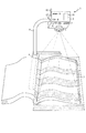
以下、本発明の好ましい実施例について、添付図面を参照して説明する。図1は、画像入出力装置1の外観斜視図である。尚、本発明の投影装置および3次元形状検出装置は、この画像入出力装置1に含まれる装置である。
Hereinafter, preferred embodiments of the present invention will be described with reference to the accompanying drawings. FIG. 1 is an external perspective view of the image input /
画像入出力装置1は、デジタルカメラとして機能するデジカメモード、ウェブカメラとして機能するwebcamモード、3次元形状を検出して立体画像を取得するための立体画像モード、湾曲した原稿等を平面化した平面化画像を取得するための平面化画像モード等の種々のモードを備えた装置である。
The image input /
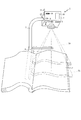
図1では、特に、立体画像モードや平面化画像モードにおいて、被写体としての原稿Pの3次元形状を検出するために、後述する画像投影部13から明暗を交互に並べてなる縞状のパターン光を投影している様子を図示している。
In FIG. 1, in order to detect the three-dimensional shape of the document P as a subject, particularly in the stereoscopic image mode and the planarized image mode, striped pattern light obtained by alternately arranging light and dark from the
画像入出力装置1は、略箱状に形成された撮像ヘッド2と、その撮像ヘッド2と一端が連結されたパイプ状のアーム部材3と、そのアーム部材3の他端と連結され、平面視略L型に形成されたベース4とを備えている。
The image input /
撮像ヘッド2は、その内部に後述する画像投影部13や画像撮像部14を内包するケースである。撮像ヘッド2の正面には、その中央部に筒状の鏡筒5と、鏡筒5の斜め上方にファインダ6と、そのファインダ6の反対側にフラッシュ7とが配置されている。また、ファインダ6とフラッシュ7との間に、後述する画像撮像部14の一部である撮像光学系21のレンズの一部が外面に露出しており、この露出部分から被写体の画像が入力される。
The
鏡筒5は、撮像ヘッド2の正面から突出し、その内部に画像投影部13の一部である投影光学系20を内包するカバーである。この鏡筒5によって、投影光学系20が保持され、全体を焦点調節のため移動可能とされ、且つ、傷つくのが防止されている。また、鏡筒5端面からは、画像投影部13の一部である投影光学系20のレンズの一部が外面に露出しており、この露出部分から投影面に向かって画像信号光が投影される。
The
ファインダ6は、撮像ヘッド2の背面から正面を通して配設される光学レンズで構成されている。撮像装置1の背面から使用者がのぞき込んだ時に、撮像光学系21がCCD22上に結像する範囲とほぼ一致する範囲が見えるようになっている。
The
フラッシュ7は、例えば、デジカメモードにおいて、必要な光量を補足するための光源であり、キセノンガスが充填された放電管で構成されている。よって、撮像ヘッド2に内蔵されているコンデンサ(図示せず)からの放電により繰り返し使用することができる。
The
また、撮像ヘッド2の上面には、手前側にレリーズボタン8と、そのレリーズボタン8の奥方にモード切替スイッチ9と、モード切替スイッチ9の反対側にモニタLCD10とが配置されている。
On the upper surface of the
レリーズボタン8は、「半押し状態」と「全押し状態」との2種類の状態に設定可能な2段階の押しボタン式のスイッチで構成されている。レリーズボタン8の状態は後述するプロセッサ15に管理されており、「半押し状態」で周知のオートフォーカス(AF)および自動露出(AF)機能が起動し、ピント、絞り、シャッタスピードが調節され、「全押し状態」で撮像等が行われる。
The
モード切替スイッチ9は、デジカメモード、webcamモード、立体画像モード、平面化画像モード、オフモード等の種々のモードに設定可能なスイッチである。モード切替スイッチ9の状態はプロセッサ15に管理されており、モード切替スイッチ9の状態がプロセッサ15によって検出されることで各モードの処理が実行される。
The
モニタLCD10は、液晶ディスプレイ(Liquid Crystal Display)で構成されており、プロセッサ15からの画像信号を受けて画像を使用者に表示する。例えば、モニタLCD10には、デジカメモードやwebcamモードにおける撮像画像や、立体画像モードにおける3次元形状検出結果画像、平面化画像モードにおける平面化画像等が表示される。
The
更に、撮像ヘッド2の側面には、その上方にRF(無線)インターフェイスとしてのアンテナ11と、撮像ヘッド2とアーム部材3とを連結する連結部材12とが配置されている。
Furthermore, an
アンテナ11は、後述するRFドライバ24を介してデジカメモードで取得した撮像画像データや立体画像モードで取得した立体画像データ等を外部インターフェイスに無線通信によって送信するものである。
The
連結部材12は、内周面に雌ねじが形成されたリング状に形成され、撮像ヘッド2の側面に回動可能に固定されている。また、アーム部材3の一端側には雄ねじが形成されている。この雌ねじと雄ねじとを嵌合させることで、撮像ヘッド2とアーム部材3とを着脱自在に連結することができると共に、撮像ヘッド2を任意の角度で固定することができるようになっている。従って、撮像ヘッド2を取り外し、通常のデジカメ(デジタルカメラ)として使用できる。
The connecting
アーム部材3は、撮像ヘッド2を所定の撮像位置に変化可能に保持するためのものであり、任意の形状に屈曲可能な蛇腹状のパイプで構成されている。よって撮像ヘッド2を任意の位置に向けることができる。
The
ベース4は、机上等の載置台に載置され、撮像ヘッド2とアーム部材3とを支持するものである。平面視略L字型に形成されているので、安定して撮像ヘッド2等を支持することができる。また、ベース4とアーム部材3とは着脱自在に連結されているので、持ち運びに便利であり、省スペースで収納することもできる。
The
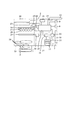
図2は、撮像ヘッド2の内部構成を模式的に示す図である。撮像ヘッド2の内部には、主に、画像投影部13と、画像撮像部14と、プロセッサ15とが内蔵されている。
FIG. 2 is a diagram schematically illustrating the internal configuration of the
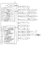
画像投影部13は、投影面に任意の投影画像を投影するためのユニットであり、投影方向に沿って、基板16と、複数個のLED17(その総称として以下「LEDアレイ17A」という)と、光源レンズ18と、投影LCD19と、投影光学系20とを備えている。尚、この画像投影部13については、図3において詳細に説明する。
The
画像撮像部14は、被写体としての原稿Pを撮像するためのユニットであり、光の入力方向に沿って、撮像光学系21と、CCD22とを備えている。
The
撮像光学系21は、複数枚のレンズで構成され、周知のオートフォーカス機能を有し、自動で焦点距離及び絞りを調整して外部からの光をCCD22上に結像する。
The imaging
CCD22は、CCD(Charge Coupled Device)素子などの光電変換素子をマトリクス状に配列して構成され、撮像光学系21を介して表面に結像される画像の光の色及び強さに応じた信号を生成し、これをデジタルデータに変換してプロセッサ15に出力する。
The
プロセッサ15には、フラッシュ7、レリーズボタン8、モード切替スイッチ9、モニタLCDドライバ23を介してモニタLCD10、RFドライバ24を介してアンテナ11、電源インターフェイス25を介してバッテリ26、外部メモリ27、キャッシュメモリ28、光源ドライバ29を介してLEDアレイ17A、投影LCDドライバ30を介して投影LCD19、CCDインターフェイス31を介してCCD22の各々が電気的に接続され、プロセッサ15によって管理されている。
The
外部メモリ27は、着脱自在なフラッシュROMであり、デジカメモードやwebcamモード、そして立体画像モードにおいて撮像した撮像画像や3次元情報を記憶する。具体的には、SDカード、コンパクトフラッシュ(登録商標)カード等を使用することができる。
The
キャッシュメモリ28は、高速な記憶装置である。例えば、デジカメモードにおいて撮像した撮像画像を高速でキャッシュメモリ28に転送し、プロセッサ15で画像処理を行ってから外部メモリ27に格納されるように使われる。具体的には、SDRAM、DDRRAM等を使用することができる。
The
尚、電源インターフェイス25はバッテリ26を、光源ドライバ29はLEDアレイ17Aを、投影LCDドライバ30は投影LED19を、CCDインターフェイス31はCCD22を各々制御する各種のIC(Integrated Circuit:集積回路)によって構成されている。
The
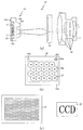
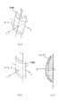
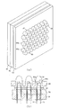
図3(a)は画像投影部13の拡大図であり、(b)は光源レンズ18の平面図であり、(c)は投影LCD19とCCD22との配置関係を示す図である。 上述した通り、画像投影部13は、投影方向に沿って、基板16と、LEDアレイ17Aと、光源レンズ18と、投影LCD19と、投影光学系20とを備えている。
3A is an enlarged view of the
基板16は、LEDアレイ17Aを実装すると共に、LEDアレイ17Aとの電気的な配線をするためのものである。具体的には、アルミ製基板に絶縁樹脂を塗布してから無電解メッキにてパターンを形成したものやカラエポ基材をコアとする単層または多層構造の基板を使用することができる。
The
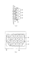
LEDアレイ17Aは、投影LCD19に向けて放射状の光を発光する光源であり、基板16上に、複数個のLED17(発光ダイオード)が千鳥状に配列され、銀ペーストを介して接着されている。また、ボンディングワイヤを介して電気的に結線されている。
The LED array 17A is a light source that emits radial light toward the
このように光源として複数個のLED17を使用することで、光源として白熱電球、ハロゲンランプ等を使用する場合に比べて、電気を光に変換する効率(電気光変換効率)を高め、同時に赤外線や紫外線の発生を抑えることができる。よって、省電力で駆動でき、節電化、長寿命化を図ることができる。また、装置の温度上昇を低減させることができる。
By using a plurality of
この様に、LED17はハロゲンランプ等に比べて熱線の発生が極めて低いので、後述する光源レンズ18や投影光学系20として、樹脂製のレンズを採用することができる。よって、ガラス製のレンズを採用する場合に比べて、各レンズ18,20を安価で軽量に構成することができる。
As described above, the
また、LEDアレイ17Aを構成する各LED17は、各々同じ発光色を発光するもので、材料にAl、In、Ga、Pの4元素を用いたアンバー色を発光するもので構成されている。よって、複数色の発光色を発光させる場合に生ずる色収差の補正を考慮する必要はなく、色収差を補正するために投影光学系20として色消しレンズを採用する必要はないので、投影光学系20の設計の自由度を向上させることができる。
Each
また、他の発光色に比べて電気光変換率が約80lumen/Wと高い4元素材料のアンバー色LEDを採用することで、一層、高輝度、節電、長寿命化を図ることができる。尚、各LED17を千鳥状に配置する事に関する効果については、図4を参照して説明する。
In addition, by using an amber LED of a four-element material having an electro-optical conversion rate as high as about 80 lumen / W compared to other luminescent colors, it is possible to achieve higher brightness, power saving, and longer life. The effect related to arranging the
具体的には、LEDアレイ17Aは59個のLED17からなり、各LED17は50mW(20mA,2.5V)で駆動され、結局、全59個のLED17は略3Wの消費電力で駆動される。また、各LED17から発光される光が、光源レンズ18、投影LCD19を通過して投影光学系20から照射される場合の光束値としての明るさは、全面照射の場合であっても25ANSIルーメン程度に設定されている。
Specifically, the LED array 17A is composed of 59
この明るさを採用することで、例えば、立体画像モードにおいて、人や動物の顔面等の被写体の3次元形状を検出する場合に、人や動物に眩しさを与えず、人や動物が目をつぶっていない状態の3次元形状を検出することができる。 By adopting this brightness, for example, in the stereoscopic image mode, when detecting the three-dimensional shape of a subject such as the face of a person or animal, the person or animal does not give glare to the person or animal. It is possible to detect a three-dimensional shape that is not collapsed.
光源レンズ18は、LEDアレイ17Aから放射状に発光される光を集光するレンズであり、その材質はアクリルに代表される光学樹脂で構成されている。
The
具体的には、光源レンズ18は、LEDアレイ17Aの各LED17に対向する位置に投影LED19側に向けて凸設された凸状のレンズ部18aと、そのレンズ部18aを支持するベース部18bと、そのベース部18bの内部空間であってLEDアレイ17Aを内包する開口に充填されるLED17の封止および基板16と光源レンズ18との接着を目的としたエポキシ封止材18cと、ベース部18bから基板16側に突設され、光源レンズ18と基板16とを接続する位置決めピン18dとを備えている。
Specifically, the
光源レンズ18は、開口の内部にLEDアレイ17Aを内包させつつ、基板16に穿設されている長孔16に位置決めピン18dを差込み、基板16上に固定される。
The
よって、省スペースで光源レンズ18を配置することができる。また、基板16にLEDアレイ17Aを実装するという機能の他に、光源レンズ18を支持するという機能を兼任させることで、光源レンズ18を支持する部品を別途必要とせず、部品の点数を削減することができる。
Therefore, the
また、各レンズ部18aは、LEDアレイ17Aの各LED17と1対1の関係で対向する位置に配置されている。
Each
よって、各LED17から発光される放射状の光は、各LED17に対向する各レンズ部18によって効率良く集光され、図に示すような指向性の高い放射光として投影LED19に照射される。この様に指向性を高めたのは、投影LCD19に略垂直に光を入射することによって、面内の透過率ムラが抑制され得るためである。また同時に、投影光学系20は、テレセントリック特性を持ち、その入射NAが0.1程度であるため、垂直±5°以内の光のみが内部の絞りを通過できるように規制されているためである。従って、LED17からの光を出射角度を垂直に揃え、且つ、±5°にほどんどの光束を入れることが画質向上の要点となる。
Therefore, the radial light emitted from each
投影LCD19は、光源レンズ18を通過して集光された光に空間変調を施して、投影光学系20に向けて画像信号光を出力する空間変調素子であって、具体的には、縦横の比率の異なる板状の液晶ディスプレイ(Liquid Crystal Display)で構成されている。
The
また、(C)に示すように、この投影LCD19を構成する各画素は、その液晶ディスプレイの長手方向に沿って一直線状に並べられた1の画素列と、その1の画素列とは液晶ディスプレイの長手方向に所定間隔ずれた他の画素列とを交互に並列に並べて配置されている。
Further, as shown in (C), each pixel constituting the
尚、(C)は紙面手前側に撮像ヘッド2の正面を向け、紙面裏側から光が投影LCD19に向けて照射され、紙面手間側からCCD22に被写体像が結像される状態であるとする。
Note that (C) is a state in which the front surface of the
このように、投影LCD19を構成する画素を長手方向に千鳥状に配置することで、長手方向と直交する方向(短手方向)において、投影LCD19によって空間変調が施される光を1/2ピッチで制御することができる。従って、細いピッチで投影パターンを制御でき、分解能を上げて高精度に3次元の形状を検出することができる。
In this way, by arranging the pixels constituting the
特に、後述する立体画像モードや平面化画像モードにおいて、被写体の3次元形状を検出すべく、被写体に向けて明暗を交互に並べてなる縞状のパターン光を投光する場合に、その縞方向を投影LCD19の短手方向に一致させることで、明暗の境界を1/2ピッチで制御することができるので、同様に高精度に3次元の形状を検出することができる。
In particular, in the stereoscopic image mode and planarized image mode, which will be described later, in order to detect a three-dimensional shape of a subject, when projecting a striped pattern light in which light and dark are alternately arranged toward the subject, the direction of the stripe is changed. By matching with the short direction of the
また、撮像ヘッド2の内部において、投影LCD19とCCD22とは、(C)に示すような関係で配置される。具体的には、投影LCD19の幅広面とCCD22の幅広面とは略同一の方向に向いて配置されているので、投影LCD19から投影面に投影されている画像をCCD22に結像させる場合に、投影画像をハーフミラー等で屈曲させることなく、そのままの状態で投影画像を結像させることができる。
In the
また、CCD22は、投影LCD19の長手方向側(画素列が延びる方向側)に配置されている。よって、特に、立体画像モードや平面化画像モードにおいて、三角測量の原理を利用して被写体の3次元形状を検出する場合には、CCD22と被写体とのなす傾きを1/2ピッチで制御することができるので、同様に高精度に3次元の形状を検出することができる。
The
投影光学系20は、投影LED19を通過した画像信号光を投影面に向けて投影する複数のレンズであり、ガラス及び樹脂の組み合わせからなるテレセントリックレンズで構成されている。テレセントリックとは、投影光学系20を通過する主光線は、入射側の空間では光軸に平行になり、射出瞳の位置は無限になる構成をいう。このようにテレセントリックにすることで、前述のように投影LCD19を垂直±5°で通過する光のみを投影し得るので、画質を向上させることができる。
The projection
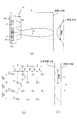
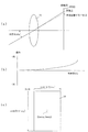
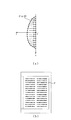
図4は、LEDアレイ17Aの配列に関する説明をするための図である。(a)は光源レンズ18を通過した光の照度分布を示す図であり、(b)はLEDアレイ17Aの配列状態を示す平面図であり、(c)は投影LCD19面における合成照度分布を示す図である。
FIG. 4 is a diagram for explaining the arrangement of the LED array 17A. (A) is a figure which shows the illumination intensity distribution of the light which passed the
(a)に示すように、光源レンズ18を通過した光は、半値拡がり半角θ(=略5°)で、(a)左側に図示するような照度分布を有する光として投影LCD19の表面に到達するように設計されている。
As shown in (a), the light that has passed through the
また、(b)に示すように、複数のLED17は基板上16に千鳥状に配列されている。具体的には、複数個のLED17をdピッチで直列に並べたLED列を、√3/2dピッチで並列に並べ、更に、そのLED列を1列おきに同じ方向に1/2d移動させた状態になるように配置されている。
Further, as shown in (b), the plurality of
換言すれば、1のLED17と、その1のLED17の周辺のLCD17との間隔はdになるように設定されている(三角格子配列)。
In other words, the distance between one
そして、このdの長さは、LED17の1つから出射された光によって投影LCD19において形成される照度分布の半値全幅(FWHM(Full Width Half Maximun))以下となる様に決定されている。
The length d is determined to be equal to or less than the full width at half maximum (FWHM (Full Width Half Maximun)) of the illuminance distribution formed in the
よって、光源レンズ18を通過して投影LCD19の表面に到達する光の合成照度分布は、(c)に示すように小さなリップルを含んだ略直線状になり、投影LCD19の面に略均一に光を照射することができる。従って、投影LCD19における照度ムラを抑制することができ、結果的に、高品質な画像を投影することができる。
Accordingly, the combined illuminance distribution of the light passing through the
図5は、画像入出力装置1の電気的なブロック図である。尚、既に上述した構成ついては、その説明を省略する。プロセッサ15は、CPU35と、ROM36と、RAM37とを備えている。
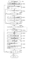
FIG. 5 is an electrical block diagram of the image input /
CPU35は、ROM36に記憶されたプログラムによる処理に応じて、RAM37を利用して、レリーズボタン8の押下げ操作の検知、CCD22から画像データの取り込み、その画像データの転送、格納、モード切替スイッチ9の状態の検出等の各種処理を行う。
The
ROM36には、カメラ制御プログラム36aと、パターン光撮影プログラム36bと、輝度画像生成プログラム36cと、コード画像生成プログラム36dと、コード境界抽出プログラム36eと、レンズ収差補正プログラム36fと、三角測量演算プログラム36gと、原稿姿勢演算プログラム36hと、平面変換プログラム36iとが格納されている。
The
カメラ制御プログラム36aは、図6に示すメイン処理を含む撮像装置1全体の制御に関するプログラムである。
The camera control program 36a is a program related to the control of the
パターン光撮影プログラム36bは、原稿Pの3次元形状を検出するために被写体にパターン光を投影した状態と、投影していない状態とを撮像するプログラムである。 The pattern light imaging program 36b is a program for imaging a state in which pattern light is projected onto a subject and a state in which the original is not projected in order to detect the three-dimensional shape of the document P.
輝度画像生成プログラム36cは、パターン光撮影プログラム36bによってパターン光を投影した状態を撮像したパターン光有画像と、パターン光を投影していない状態を撮像したパターン光無画像との差分をとり、投影されたパターン光の輝度画像を生成するプログラムである。 The luminance image generation program 36c takes the difference between the pattern light presence image obtained by imaging the pattern light projected by the pattern light imaging program 36b and the pattern light no image obtained by imaging the state where the pattern light is not projected. This is a program for generating a luminance image of the patterned light.
また、パターン光は複数種類のものが時系列に投影され各パターン光毎に撮像され、撮像された複数枚のパターン光有画像の各々とパターン光無画像との差分がとられ、複数種類の輝度画像が生成される。 In addition, a plurality of types of pattern light are projected in time series and imaged for each pattern light, and the difference between each of the plurality of captured pattern light images and the pattern light no image is obtained. A luminance image is generated.
コード画像生成プログラム36dは、輝度画像生成プログラム36cによって生成される複数枚の輝度画像を重ね合わせ、各画素毎に所定のコードを割り当てたコード画像を生成するプログラムである。
The code
コード境界抽出プログラム36eは、コード画像生成プログラム36dによっって生成されるコード画像と、輝度画像生成プログラム36cによって生成される輝度画像とを利用して、コードの境界座標をサブピクセル精度で求めるプログラムである。
The code
レンズ収差補正プログラム36fは、コード境界抽出プログラム36eによってサブピクセル精度で求められているコードの境界座標に対して、撮像光学系20の収差補正を行うプログラムである。
The lens
三角測量演算プログラム36gは、レンズ収差補正プログラム36fによって収差補正がなされたコードの境界座標から、その境界座標に関する実空間の3次元座標を演算するプログラムである。
The triangulation calculation program 36g is a program for calculating the three-dimensional coordinates of the real space related to the boundary coordinates from the boundary coordinates of the code subjected to the aberration correction by the lens
原稿姿勢演算プログラム36hは、三角測量演算プログラム36gで演算された3次元座標から原稿Pの3次元形状を推定して求めるプログラムである。 The document orientation calculation program 36h is a program for estimating the three-dimensional shape of the document P from the three-dimensional coordinates calculated by the triangulation calculation program 36g.
平面変換プログラム36iは、原稿姿勢演算プログラム36hで演算される原稿Pの3次元形状に基づき、原稿Pの正面から撮像したような平面化画像を生成するプログラムである。 The plane conversion program 36i is a program that generates a planarized image that is captured from the front of the document P, based on the three-dimensional shape of the document P calculated by the document orientation calculation program 36h.
RAM37には、パターン光有画像格納部37aと、パターン光無画像格納部37bと、輝度画像格納部37cと、コード画像格納部37dと、コード境界座標格納部37eと、ID格納部37fと、収差補正座標格納部37gと、3次元座標格納部37hと、原稿姿勢演算結果格納部37iと、平面変換結果格納部37jと、投影画像格納部37kと、ワーキングエリア37lとが記憶領域として割り当てられている。
The
パターン光有画像格納部37aは、パターン光撮影プログラム36bによって原稿Pにパターン光を投影した状態を撮像したパターン光有画像を格納する。パターン光無画像格納部37bは、パターン光撮影プログラム36bによって原稿Pにパターン光を投影していない状態を撮像したパターン光無画像を格納する。 The pattern light present image storage unit 37a stores a pattern light present image obtained by imaging the state in which the pattern light is projected onto the document P by the pattern light photographing program 36b. The pattern light no image storage unit 37b stores a pattern light no image obtained by imaging the state in which the pattern light is not projected onto the document P by the pattern light photographing program 36b.
輝度画像格納部37cは、輝度画像生成プログラム36cによって生成される輝度画像を格納する。コード画像格納部37dは、コード画像生成プログラム36dによって生成されるコード画像を格納する。コード境界座標格納部37eは、コード境界抽出プログラム36eによって、抽出されるサブピクセル精度で求められた各コードの境界座標を格納する。ID格納部37fは、境界を有する画素位置において明暗の変化を有する輝度画像に割り当てられるID等を格納する。収差補正座標格納部37gは、レンズ収差補正プログラム36fによって収差補正がなされたコードの境界座標を格納する。3次元形状座標格納部37hは、三角測量演算プログラム36gによって演算される実空間の3次元座標を格納する。
The luminance
原稿姿勢演算結果格納部37iは、原稿姿勢演算プログラム36hによって演算される原稿Pの3次元形状に関するパラメータを格納する。平面変換結果格納部37jは、平面変換プログラム36iよって生成される平面変換結果を格納する。投影画像格納部37kは、画像投影部13から投影する画像情報を格納する。ワーキングエリア37lは、CPU15での演算のために一時的に使用するデータを格納する。
The document orientation calculation result storage unit 37i stores parameters related to the three-dimensional shape of the document P calculated by the document orientation calculation program 36h. The plane conversion
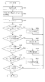
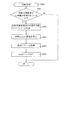
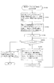
図6は、メイン処理のフローチャートである。尚、このメイン処理におけるデジカメ処理(S605)、webcam処理(S607)、立体画像処理(S607)、平面化画像処理(S611)の各処理についての詳細は後述する。 FIG. 6 is a flowchart of the main process. Details of the digital camera processing (S605), webcam processing (S607), stereoscopic image processing (S607), and planarized image processing (S611) in the main processing will be described later.
メイン処理では、まず、電源が起動されると(S601)、プロセッサ15やその他のインターフェイス等が初期化される(S602)。
In the main process, first, when the power supply is activated (S601), the
そして、モード切替スイッチ9の状態を判別するキースキャンが行われ(S603)、モード切替スイッチ9の設定がデジカメモードか否かが判断され(S604)、デジカメモードであれば(S604:Yes)、後述するデジカメ処理に移行する(S605)。
Then, a key scan for determining the state of the
一方、デジカメモードでなければ(S604:No)、モード切替スイッチ9の設定がwebcamモードか否かが判断され(S606)、webcamモードであれば(S606:Yes)、後述するwebcam処理に移行する(S607)。
On the other hand, if it is not the digital camera mode (S604: No), it is determined whether or not the setting of the
一方、webcamモードでなければ(S605:No)、モード切替スイッチ9の設定が立体画像モードか否かが判断され(S608)、立体画像モードであれば(S608:Yes)、後述する立体画像処理に移行する(S609)。
On the other hand, if it is not the webcam mode (S605: No), it is determined whether the setting of the
一方、立体画像モードでなければ(S608:No)、モード切替スイッチ9の設定が平面化画像モードか否かが判断され(S610)、平面化画像モードであれば(S610:Yes)、後述する平面化画像処理に移行する(S611)。
On the other hand, if it is not the stereoscopic image mode (S608: No), it is determined whether or not the setting of the
一方、平面化画像モードでなければ(S610:No)、モード切替スイッチ9がオフモードか否かが判断され(S612)、オフモードでなければ(S612:No)、S603からの処理を繰り返し、オフモードであれば(S612:Yes)、当該処理を終了する。
On the other hand, if it is not the planar image mode (S610: No), it is determined whether or not the
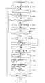
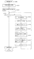
図7は、デジカメ処理(図6のS605)のフローチャートである。デジカメ処理は、画像撮像部14によって撮像した画像を取得する処理である。
FIG. 7 is a flowchart of the digital camera process (S605 in FIG. 6). The digital camera process is a process for acquiring an image captured by the
この処理では、まず、CCD22に高解像度設定信号を送信する(S701)。これにより高品質の撮像画像を使用者に提供することができる。 In this process, first, a high resolution setting signal is transmitted to the CCD 22 (S701). Thereby, a high quality captured image can be provided to the user.
次に、モニタLCD10にファインダ画像(ファインダ6を介して見える範囲の画像)を表示する(S702)。よって、使用者は、ファインダ6を覗き込むことなく、モニタLCD10に表示された画像によって実際の撮像の前に、撮像画像(撮像範囲)を確認することができる。
Next, a finder image (an image in a range visible through the finder 6) is displayed on the monitor LCD 10 (S702). Therefore, the user can confirm the captured image (imaging range) before actual imaging with the image displayed on the
次に、レリーズボタン8をスキャンし(S703a)、レリーズボタン8が半押しされたか否かを判断する(S703b)。半押しされていれば(S703b:Yes)、オートフォーカス(AF)および自動露出(AE)機能を起動し、ピント、絞り、シャッタスピードを調節する(S703c)。尚、半押しされていなければ(S703b:No)、S703aからの処理を繰り返す。
Next, the
次に、再び、レリーズボタン8をスキャンし(S703d)、レリーズボタン8が全押しされたか否かを判断する(S703e)。全押しされていれば(S703e:Yes)、フラッシュモードか否かを判断する(S704)。
Next, the
その結果、フラッシュモードであれば(S704:Yes)、フラッシュ7を投光して(S705)、撮影し(S706)、フラッシュモードでなければ(S704:No)、フラッシュ7を投光することなく撮影する(S706)。尚、S703eの判断において、全押しされていなければ(S703e:No)、S703aからの処理を繰り返す。
As a result, if the flash mode is selected (S704: Yes), the
次に、撮影した撮像画像をCCD22からキャッシュメモリ28に転送し(S707)、キャッシュメモリ28に記憶された撮像画像をモニタLCD10に表示する(S708)。このように、撮像画像をキャッシュメモリ28に転送することでメインメモリに転送する場合に比較して、撮像画像を高速にモニタLCD10に表示させることができる。そして、その撮像画像を外部メモリ27に格納する(S709)。
Next, the captured image is transferred from the
最後に、モード切替スイッチ9に変化が無いか否かを判断し(S710)、そ変化が無ければ(S710:Yes)、S702からの処理を繰り返し、変化があれば(S710:No)、当該処理を終了する。
Finally, it is determined whether or not the
図8は、webcam処理(図6のS607)のフローチャートである。webcam処理は、画像撮像部14で撮像した撮像画像(静止画および動画を含む)を外部ネットワークに送信する処理である。尚、本実施例では、撮像画像として動画を外部ネットワークに送信する場合を想定している。
FIG. 8 is a flowchart of the webcam process (S607 in FIG. 6). The webcam process is a process of transmitting a captured image (including a still image and a moving image) captured by the
この処理では、ます、CCD22に低解像度設定信号を送信し(S801)、周知のオートフォーカス及び自動露出機能を起動して、ピント、絞り、シャッター速度を調節した後に(S802)、撮影を開始する(S803)。 In this process, a low resolution setting signal is first transmitted to the CCD 22 (S801), the well-known autofocus and automatic exposure functions are activated, and the focus, aperture, and shutter speed are adjusted (S802), and shooting is started. (S803).
そして、撮影された撮像画像をモニタLCD10に表示し(S804)、ファインダ画像を投影画像格納部37kに格納し(S805)、後述する投影処理を行い(S806)、投影画像格納部37kに格納されている画像を投影面に投影する。
Then, the captured image is displayed on the monitor LCD 10 (S804), the finder image is stored in the projection
また、撮像画像をCCD22からキャッシュメモリ28に転送し(S807)、キャッシュメモリ28に転送された撮像画像をRFインターフェイスを介して外部ネットワークに送信する(S808)。
The captured image is transferred from the
そして、最後に、モード切替スイッチ9に変化が無いか否かを判断し(S809)、変化が無ければ(S809:Yes)、S802からの処理を繰り返し、変化があれば(S809:No)、当該処理を終了する。
Finally, it is determined whether or not the
図9は投影処理(図8のS806)のフローチャートである。この処理は、投画像投影部13から影画像格納部37kに格納されている画像を投影面に投影する処理である。この処理では、まず、投影画像格納部37kに画像が格納されているか否かを確認する(S901)。格納されていれば(S901:Yes)、投影画像格納部37kに格納されている画像を投影LCDドライバ30に転送し(S902)、投影LCDドライバ30から、その画像に応じた画像信号を投影LCD19に送り、投影LCDに画像を表示する(S903)。
FIG. 9 is a flowchart of the projection process (S806 in FIG. 8). This process is a process of projecting the image stored in the shadow
次に、光源ドライバ29を駆動し(S904)、その光源ドライバ29からの電気信号によってLEDアレイ17Aを点灯し(S905)、当該処理を終了する。
Next, the
こうして、LEDアレイ17Aが点灯すると、LEDアレイ17Aから発光する光は、光源レンズ18を介して投影LCD19に到達し、投影LCD19において、投影LCDドライバ30から送信される画像信号に応じた空間変調が施され、画像信号光として出力される。そして、その投影LCD19から出力される画像信号光は、投影光学系20を介して投影面に投影画像として投影される。
Thus, when the LED array 17A is turned on, the light emitted from the LED array 17A reaches the
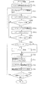
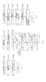
図10は立体画像処理(図6のS609)のフローチャートである。立体画像処理は、被写体の3次元形状を検出し、その立体画像としての3次元形状検出結果画像を取得、表示、投影する処理である。 FIG. 10 is a flowchart of the stereoscopic image processing (S609 in FIG. 6). The stereoscopic image processing is processing for detecting a three-dimensional shape of a subject and acquiring, displaying, and projecting a three-dimensional shape detection result image as the stereoscopic image.
この処理では、まず、CCD22に高解像度設定信号を送信し(S1001)、モニタLCD10にファインダ画像を表示する(S1002)。 In this process, first, a high resolution setting signal is transmitted to the CCD 22 (S1001), and a finder image is displayed on the monitor LCD 10 (S1002).
次に、レリーズボタン8をスキャンし(S1003a)、レリーズボタン8が半押しされたか否かを判断する(S1003b)。半押しされていれば(S1003b:Yes)、オートフォーカス(AF)および自動露出(AE)機能を起動し、ピント、絞り、シャッタスピードを調節する(S1003c)。尚、半押しされていなければ(S1003b:No)、S1003aからの処理を繰り返す。
Next, the
次に、再び、レリーズボタン8をスキャンし(S1003d)、レリーズボタン8が全押しされたか否かを判断する(S1003e)。全押しされていれば(S1003e:Yes)、フラッシュモードか否かを判断する(S1003f)。
Next, the
その結果、フラッシュモードであれば(S1003f:Yes)、フラッシュ7を投光して(S1003g)、撮影し(S1003h)、フラッシュモードでなければ(S1003f:No)、フラッシュ7を投光することなく撮影する(S1003h)。尚、S1003eの判断において、全押しされていなければ(S1003e:No)、S1003aからの処理を繰り返す。
As a result, if the flash mode is selected (S1003f: Yes), the
次に、後述する3次元形状検出処理を行い、被写体の3次元形状を検出する(S1006)。 Next, a three-dimensional shape detection process described later is performed to detect the three-dimensional shape of the subject (S1006).
次に、3次元形状検出処理(S1006)における3次元形状検出結果を外部メモリ27に格納し(S1007)、3次元形状検出結果をモニタLCD10に表示する(S1008)。尚、この3次元形状検出結果とは、各計測頂点の実空間における3次元座標(XYZ)の集合体として表示する。 Next, the three-dimensional shape detection result in the three-dimensional shape detection process (S1006) is stored in the external memory 27 (S1007), and the three-dimensional shape detection result is displayed on the monitor LCD 10 (S1008). The three-dimensional shape detection result is displayed as an aggregate of three-dimensional coordinates (XYZ) in the real space of each measurement vertex.
次に、3次元形状検出結果としての計測頂点をポリゴンで結んでそのサーフェスを表示した立体画像(3DのCG画像)としての3次元形状検出結果画像を投影画像格納部37kに格納し(S1009)、図8のS806の投影処理と同様な投影処理を行う(S1010)。尚、この場合には、図18において説明する投影LCD19上の座標を3次元空間座標に変換する式の逆関数を利用して、求められた3次元座標に対する投影LCD19上の座標を求めることで、3次元形状結果座標を投影面に投影させることができる。
Next, a three-dimensional shape detection result image as a three-dimensional image (3D CG image) displaying the surface by connecting the measurement vertices as a three-dimensional shape detection result with a polygon is stored in the projection
そして、モード切替スイッチ9に変化が無いか否かを判断し(S1011)、変化が無ければ(S1011:Yes)、S702からの処理を繰り返し、変化があれば(S1011:No)、当該処理を終了する。
Then, it is determined whether or not the
図11(a)は、上述した3次元形状検出処理(図10のS1006)において、3次元形状を検出するために利用する空間コード法の原理を説明するための図であり、(b)は(a)とは異なるパターン光を示す図である。パターン光にはこれら(a)または(b)のいずれを用いても良く、更には、多階調コードであるグレイレベルコードを用いても良い。 FIG. 11A is a diagram for explaining the principle of the spatial code method used to detect a three-dimensional shape in the above-described three-dimensional shape detection process (S1006 in FIG. 10). It is a figure which shows the pattern light different from (a). Either (a) or (b) may be used for the pattern light, and further, a gray level code which is a multi-tone code may be used.
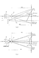
尚、この空間コード法につての詳細は、佐藤宏介、他1名、「空間コード化による距離画像入力」、電子通信学会論文誌、85/3Vol.J 68−D No3 p369〜375に詳細に開示されている。 Details of this spatial coding method are described by Kosuke Sato and one other, “Distance Image Input by Spatial Coding”, IEICE Transactions, 85/3 Vol. J 68-D No3 p369-375.
空間コード法は、投影光と観測画像間の三角測量に基づいて被写体の3次元形状を検出する方法の1種であり、(a)に示すように、投影光源Lと観測器Oとを距離Dだけ離して設置し、空間を細長い扇状領域に分割しコード化することを特徴とする。 The spatial code method is one type of method for detecting the three-dimensional shape of a subject based on triangulation between projected light and an observed image. As shown in (a), the distance between the projection light source L and the observation device O is determined. It is characterized in that it is set apart by D, and the space is divided into long and narrow fan-shaped regions and coded.
図中の3枚のマスクパターンA,B,CをMSBから順番に投影すると、各扇状領域はマスクによって明「1」と暗「0」とにコード化される。例えば、点Pを含む領域は、マスクA,Bでは光が当たらず、マスクCでは明になるので、001(A=0、B=0、C=1)とコード化される。 When the three mask patterns A, B, and C in the figure are projected in order from the MSB, each fan-shaped area is coded into bright “1” and dark “0” by the mask. For example, since the area including the point P is not exposed to light in the masks A and B and bright in the mask C, it is encoded as 001 (A = 0, B = 0, C = 1).
各扇状の領域には、その方向φに相当するコードが割り当てられ、それぞれを1本のスリット光線とみなすことができる。そこで各マスクごとに情景を観測機器としてのカメラで撮影し、明暗パターンを2値化してメモリの各ビットプレーンを構成していく。 Each fan-shaped region is assigned a code corresponding to the direction φ, and each can be regarded as one slit beam. Therefore, the scene is photographed for each mask with a camera as an observation device, and the bit plane of the memory is constructed by binarizing the light / dark pattern.
こうして、得られた多重ビットプレーン画像の横方向の位置(アドレス)は、観測方向θに相当し、このアドレスのメモリの内容は投影光コード、即ち、φを与える。このθとφとから注目点の座標を決定する。 Thus, the horizontal position (address) of the obtained multiple bit-plane image corresponds to the observation direction θ, and the contents of the memory at this address give the projected light code, that is, φ. The coordinates of the point of interest are determined from θ and φ.
また、この方法で使用するマスクパターンとしては、(a)ではマスクパターンA,B,Cのような純2進コードを用いる場合を図示しているが、マスクの位置ズレが起こると領域の境界で大きな誤差が生ずる危険性がある。 In addition, as a mask pattern used in this method, a case where a pure binary code such as mask patterns A, B, and C is used is illustrated in FIG. There is a risk that a large error will occur.
例えば、(a)の点Qは領域3(011)と領域4(100)の境界を示しているが、もしマスクAの1がずれ込むと領域7(111)のコードが生ずる可能性がある。換言すれば、隣接する領域間でハミング距離が2以上のところで、大きな誤差が発生する可能性がある。 For example, the point Q in (a) indicates the boundary between the region 3 (011) and the region 4 (100), but if 1 of the mask A is shifted, the code in the region 7 (111) may be generated. In other words, a large error may occur when the Hamming distance is 2 or more between adjacent regions.
そこで、この方法で使用するマスクパターンとしては、(b)に示すように、隣接する領域間でハミング距離が常に1であるコードを使うことで、上述したようなコード化誤差を避けることができるとされている。 Therefore, as the mask pattern used in this method, as shown in (b), by using a code whose hamming distance is always 1 between adjacent regions, the coding error as described above can be avoided. It is said that.
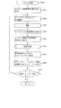
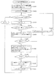
図12(a)は、3次元形状検出処理(図10のS1006)のフローチャートである。この処理では、まず、撮像処理を行う(S1210)。この撮像処理は、図11(a)に示す複数枚の純2進コードのマスクパターンを利用して画像投影部13から、明暗を交互に並べてなる縞状のパターン光(図1参照)を時系列的に被写体に投影し、各パターン光が投影されている状態を撮像したパターン光有画像と、パターン光が投影されていな状態を撮像したパターン光無画像とを取得する処理である。
FIG. 12A is a flowchart of the three-dimensional shape detection process (S1006 in FIG. 10). In this process, first, an imaging process is performed (S1210). This imaging process uses a plurality of pure binary code mask patterns shown in FIG. 11 (a) to emit striped pattern light (see FIG. 1) in which light and dark are alternately arranged from the
撮像処理を終了すると(S1210)、3次元計測処理を行う(S1220)。3次元計測処理は、撮像処理によって取得したパターン光有画像とパターン光無画像とを利用して、実際に被写体の3次元形状を計測する処理である。こうして、3次元計測処理を終了すると(S1220)、当該処理を終了する。 When the imaging process is completed (S1210), a three-dimensional measurement process is performed (S1220). The three-dimensional measurement process is a process of actually measuring the three-dimensional shape of the subject using the pattern light existence image and the pattern light no image acquired by the imaging process. Thus, when the three-dimensional measurement process ends (S1220), the process ends.
図12(b)は、撮像処理(図12(a)のS1210)のフローチャートである。この処理は、パターン光撮影プログラム36aに基づき実行され、まず、画像投影部13からパターン光を投影することなく、画像撮像部14によって被写体を撮像することで、パターン光無画像を取得する(S1211)。尚、取得したパターン光無画像はパターン光無画像格納部37bに格納される。
FIG. 12B is a flowchart of the imaging process (S1210 in FIG. 12A). This process is executed based on the pattern light imaging program 36a. First, the
次に、カウンタiを初期化し(S1212)、そのカウンタiの値が最大値imaxか否かを判断する(S1213)。尚、最大値imaxは使用するマスクパターンの数によって決定される。例えば、8種類のマスクパターンを使用する場合には、最大imax(=8)となる。 Next, the counter i is initialized (S1212), and it is determined whether or not the value of the counter i is the maximum value imax (S1213). The maximum value imax is determined by the number of mask patterns to be used. For example, when 8 types of mask patterns are used, the maximum is imax (= 8).
そして、判断の結果、カウンタiの値が最大値imaxより小さい場合には(S1213:Yes)、使用するマスクパターンの内、i番のマスクパターンを投影LCD19に表示し、そのi番のマスクパターンによって投影されるi番のパターン光を投影面に投影し(S1214)、そのパターン光が投影されている状態を画像撮像部14によって撮影する(S1215)。
If it is determined that the value of the counter i is smaller than the maximum value imax (S1213: Yes), the i-th mask pattern among the mask patterns to be used is displayed on the
こうして、被写体にi番のパターン光が投影された状態を撮像したパターン光有画像を取得する。尚、取得したパターン光有画像は、パターン光有画像格納部37aに格納される。 In this way, a pattern light existence image obtained by imaging the state in which the i-th pattern light is projected onto the subject is acquired. The acquired pattern light existence image is stored in the pattern light existence image storage unit 37a.
撮影を終了すると、i番のパターン光の投影を終了し(S1216)、次のパターン光を投影すべく、カウンタiに「1」を加算して(S1217)、S1213からの処理を繰り返す。 When the photographing is finished, the projection of the i-th pattern light is finished (S1216), "1" is added to the counter i to project the next pattern light (S1217), and the processing from S1213 is repeated.
そして、カウンタiの値が最大値imaxより大きいと判断すると(S1213:No)、当該処理を終了する。即ち、この撮像処理においては、1枚のパターン光無画像と、最大値imax枚のパターン光有画像とを取得することになる。 If it is determined that the value of the counter i is greater than the maximum value imax (S1213: No), the process ends. That is, in this imaging process, one pattern light no image and the maximum value imax pattern light existence images are acquired.
図12(c)は、3次元計測処理(図12(a)のS1220)のフローチャートである。この処理は、輝度画像生成プログラム36cに基づき実行され、まず、輝度画像を生成する(S1221)。ここで、輝度は、YCbCr空間におけるY値であり、各画素のRGB値よりY=0.2989・R+0.5866・G+0.1145・Bから計算される値である。各画素についてY値を求めることにより、各パターン光有及び無し画像に関する輝度画像を生成する。生成した輝度画像は、輝度画像格納部37cに格納される。また、パターン光の番号に対応した番号を各輝度画像に割り付けておく。
FIG. 12C is a flowchart of the three-dimensional measurement process (S1220 in FIG. 12A). This process is executed based on the luminance image generation program 36c, and first generates a luminance image (S1221). Here, the luminance is a Y value in the YCbCr space, and is a value calculated from Y = 0.22989 · R + 0.5866 · G + 0.1145 · B from the RGB value of each pixel. By obtaining the Y value for each pixel, a luminance image relating to the image with and without pattern light is generated. The generated luminance image is stored in the luminance
次に、コード画像生成プログラム36dにより、上述した空間コード法を利用して、生成した輝度画像を組み合わせることで、各画素毎にコード化されたコード画像を生成する(S1222)。
Next, the code
このコード画像は、輝度画像格納部37cに格納したパターン光有り画像に関する輝度画像の各画素について、あらかじめ設定した輝度閾値と比較し、その結果を結合させることで生成することができる。生成されたコード画像はコード画像格納部37dに格納される。
The code image can be generated by comparing each pixel of the luminance image related to the image with pattern light stored in the luminance
次に、コード境界抽出プログラム36eにより、後述するコード境界座標検出処理を行い(S1223)、各画素毎に割り当てられたコードの境界座標をサブピクセル精度で検出する。
Next, a code boundary coordinate detection process described later is performed by the code
次に、レンズ収差補正プログラム36fにより、レンズ収差補正処理を行う(S1224)。この処理によって、撮像光学系21の歪みなどの影響で誤差を含んでいるS1223で検出されるコード境界座標の誤差を補正することができる。
Next, lens aberration correction processing is performed by the lens
次に、三角測量演算プログラム36gにより、三角測量原理による実空間変換処理を行う(S1225)。この処理によって収差補正が施された後のCCD空間上のコード境界座標は、実空間における3次元座標に変換され、3次元形状検出結果としての3次元座標が求められる。 Next, real space conversion processing based on the triangulation principle is performed by the triangulation calculation program 36g (S1225). The code boundary coordinates on the CCD space after the aberration correction is performed by this processing are converted into the three-dimensional coordinates in the real space, and the three-dimensional coordinates as the three-dimensional shape detection result are obtained.
図13は、コード境界座標検出処理(図12のS1223)の概略を説明するための図である。上側の図は、CCD空間において実際のパターン光の明暗の境界を境界線Kで示し、そのパターン光を上述した空間コード法でコード化し、1のコードと他のコードとの境界を図中太線で示した図である。 FIG. 13 is a diagram for explaining the outline of the code boundary coordinate detection process (S1223 in FIG. 12). In the upper diagram, the bright and dark boundaries of the actual pattern light in the CCD space are indicated by the boundary line K. The pattern light is encoded by the spatial code method described above, and the boundary between one code and another code is indicated by a bold line in the figure. It is the figure shown by.
即ち、上述した空間コード法におけるコード化は、各画素単位で行われるため、実際のパターン光の境界線Kと、コード化された境界(図中太線)とではサブピクセル精度の誤差が生ずる。そこで、このコード境界座標検出処理は、コードの境界座標をサブピクセル精度で検出することを目的とする。 That is, since the coding in the spatial coding method described above is performed on a pixel-by-pixel basis, an error in sub-pixel accuracy occurs between the boundary line K of the actual pattern light and the coded boundary (thick line in the figure). Therefore, the purpose of this code boundary coordinate detection process is to detect code boundary coordinates with sub-pixel accuracy.
この処理では、まず、ある検出位置(以下「curCCDX」と称す)において、ある着目コード(以下「curCode」という)から他のコードに変化する第1画素Gを検出する(第1画素検出工程)。 In this process, first, at a certain detection position (hereinafter referred to as “curCDX”), a first pixel G that changes from a certain target code (hereinafter referred to as “curCode”) to another code is detected (first pixel detection step). .
例えば、curCCDXにおいて、上から順番に各画素を検出すると、境界(太線)まではcurCodeを有する画素であるが、境界の次の画素、即ち、第1画素Gにおいて、curCodeは変化しているので、これを第1画素Gとして検出する。 For example, in curCDXX, when each pixel is detected in order from the top, it is a pixel having curCode up to the boundary (thick line), but curCode changes in the pixel next to the boundary, that is, the first pixel G. This is detected as the first pixel G.
次に、その第1画素Gの画素位置において、図12のS1221において輝度画像格納部37cに格納された輝度画像の内から、明暗の変化を持つ輝度画像の全部を抽出する(輝度画像抽出工程)。
Next, at the pixel position of the first pixel G, all of the luminance images having a change in brightness are extracted from the luminance images stored in the luminance
次に、近似に利用するための画素領域を特定するために検出位置を「2」左側に移動させ、検出位置curCCDX−2の位置において、コード画像を参照して、着目コード(curCode)から他のコードに変化する画素(境界画素(curCCDX−2の検出位置では画素H))を探し、その画素を中心に予め定めた範囲(本実施例の場合Y軸方向に−3画素と+2画素の範囲)の画素範囲を特定する(画素領域特定手段の一部)。 Next, in order to specify a pixel area to be used for approximation, the detection position is moved to the left by “2”, and the code image is referred to at the position of the detection position curCDXX-2 to change from the target code (curCode). Pixel (boundary pixel (pixel H at the detection position of cur CCDX-2)) is searched for, and a predetermined range centered on that pixel (in the present embodiment, -3 pixels and +2 pixels in the Y-axis direction) Range) is specified (part of the pixel area specifying means).
次に、その予め定めた範囲内において、図中の下側の左側のグラフに示すように、Y方向の画素位置と輝度とに関する近似式(図中実線で示す)を求め、その近似式における輝度閾値bThとの交点におけるY座標Y1を求める(境界座標検出工程の一部)。 Next, within the predetermined range, as shown in the lower left graph in the figure, an approximate expression (shown by a solid line) in the Y direction is obtained, and the approximate expression The Y coordinate Y1 at the intersection with the luminance threshold value bTh is obtained (part of the boundary coordinate detection step).
尚、輝度閾値bThは、予め定められた範囲内から算出(例えば、各画素の輝度の平均の2分の1)しても良く、予め与えられた固定値であっても良い。これにより、明と暗との境界をサブピクセル精度で検出することができる。 Note that the luminance threshold value bTh may be calculated from a predetermined range (for example, one half of the average luminance of each pixel) or may be a fixed value given in advance. As a result, the boundary between light and dark can be detected with sub-pixel accuracy.
次に、検出位置をcurCCDX−2から「1」右側に移動させ、curCCDX−1において上述したのと同様な処理を行い、curCCDX−1における代表値を求める(境界座標検出工程の一部)。 Next, the detection position is moved to the right side of “1” from curCCDX-2, and the same processing as described above is performed in curCCDX-1 to obtain a representative value in curCCDX-1 (part of the boundary coordinate detection step).
このように、境界画素を中心にY軸方向に予め定めた範囲と、X軸方向におけるcurCCDX−2からcurCCDX+2の範囲とで構成される画素領域(図中右下がり斜線部参照)において、各検出位置における代表値を求める。 In this manner, each detection is performed in a pixel area (see the lower right hatched portion in the figure) composed of a predetermined range in the Y-axis direction centering on the boundary pixel and a range of curCCDX-2 to curCCDX + 2 in the X-axis direction. The representative value at the position is obtained.
これまでの処理をcurCodeから他のコードへ変化する画素を持つ輝度画像の全てに行い、各輝度画像についての代表値の加重平均値を最終的にcurCodeにおける境界座標として採用する(境界座標検出工程の一部)。 The above processing is performed on all luminance images having pixels that change from curCode to another code, and a weighted average value of representative values for each luminance image is finally adopted as boundary coordinates in curCode (boundary coordinate detection step) Part of).
これにより、コードの境界座標を高精度にサブピクセル精度で検出することができ、この境界座標を利用して上述した三角測量原理による実空間変換処理(図12のS1225)を行うことで、高精度に被写体の3次元形状を検出することができる。 As a result, the boundary coordinates of the code can be detected with high accuracy with sub-pixel precision, and by performing the real space conversion process (S1225 in FIG. 12) based on the above-described triangulation principle using the boundary coordinates, The three-dimensional shape of the subject can be detected with high accuracy.
また、このように輝度画像に基づき算出される近似式を利用して境界座標をサブピクセル精度で検出することができるため、従来のように撮像枚数を増加させることもなく、また、純2進コードで明暗付けられたパターン光であっても良く、特殊なパターン光であるグレイコードを用いる必要はない。 In addition, since the boundary coordinates can be detected with sub-pixel accuracy by using the approximate expression calculated based on the luminance image in this way, the number of images to be captured is not increased as in the prior art, and pure binary. Pattern light brightened and darkened by a code may be used, and it is not necessary to use a gray code which is a special pattern light.
尚、本実施例では、各検出位置において境界画素を中心にY軸方向に「−3」から「+2」の範囲と、X軸方向における検出位置としてのcurCCDX−2からcurCCDX+2の範囲とで構成される領域を、近似を求めるための画素領域として説明したが、この画素領域のY軸、X軸の範囲はこれらに限定されるものではない。例えば、curCCDXの検出位置における境界画素を中心としたY軸方向への所定範囲だけを画素領域としても良い。 In this embodiment, each detection position is composed of a range from “−3” to “+2” in the Y-axis direction around the boundary pixel, and a range from curCCDX-2 to curCCDX + 2 as the detection position in the X-axis direction. Although the region to be processed has been described as a pixel region for obtaining approximation, the ranges of the Y axis and the X axis of the pixel region are not limited to these. For example, only a predetermined range in the Y-axis direction centering on the boundary pixel at the curCDX detection position may be set as the pixel region.
図14は、コード境界座標検出処理(図12のS1223)のフローチャートである。この処理は、コード境界抽出プログラム36eに基づき実行され、まず、CCD空間におけるコード境界座標列の各要素を初期化し(S1401)、curCCDXを開始座標に設定する(S1402)。
FIG. 14 is a flowchart of the code boundary coordinate detection process (S1223 in FIG. 12). This process is executed based on the code
次に、curCCDXが終了座標以下か否かを判断し(S1403)、終了座標以下であれば(S1403:Yes)、curCodeを「0」に設定する(S1404)。即ち、curCodeは当初、最小値に設定される。 Next, it is determined whether curCCDX is equal to or less than the end coordinate (S1403). If it is equal to or less than the end coordinate (S1403: Yes), curCode is set to “0” (S1404). That is, curCode is initially set to a minimum value.
次に、curCodeが最大コードより小さいか否かを判断する(S1405)。curCodeが最大コードより小さければ(S1405:Yes)、curCCDXにおいてコード画像を参照して、curCodeの画素を探し(S1406)、curCodeの画素が存在するか否かを判断する(S1407)。 Next, it is determined whether curCode is smaller than the maximum code (S1405). If the curCode is smaller than the maximum code (S1405: Yes), the curCCDX refers to the code image to search for the curCode pixel (S1406), and determines whether the curCode pixel exists (S1407).
その結果、curCodeの画素が存在していれば(S1407:Yes)、curCCDXにおいて、そのcurCodeよりも大きなCodeの画素をコード画像を参照して探し(S1408)、そのcurCodeよりも大きなcurCodeの画素が存在するか否かを判断する(S1409)。 As a result, if a curCode pixel exists (S1407: Yes), the curCDXX searches for a code pixel larger than the curCode by referring to the code image (S1408), and a curCode pixel larger than the curCode is found. It is determined whether or not it exists (S1409).
その結果、curCodeよりも大きなCodeの画素が存在していれば(S1409:Yes)、後述する境界をサブピクセル精度で求める処理を行う(S1410)。そして、次のcurCodeについて境界座標を求めるべく、curCodeに「1」を加算して(S1411)、S1405からの処理を繰り返す。 As a result, if there is a pixel with a code larger than curCode (S1409: Yes), a process for obtaining a later-described boundary with subpixel accuracy is performed (S1410). Then, in order to obtain boundary coordinates for the next curCode, “1” is added to curCode (S1411), and the processing from S1405 is repeated.
即ち、境界は、curCodeを有する画素の画素位置またはcurCodeよりも大きなCodeの画素の画素位置に存在しているため、本実施例では、暫定的に境界は、curCodeより大きなcurCodeの画素の画素位置にあると仮定して処理を進めるものである。 That is, since the boundary exists at the pixel position of the pixel having the curCode or the pixel position of the pixel of the Code that is larger than the curCode, in the present embodiment, the boundary is temporarily the pixel position of the pixel of the CurCode that is larger than the curCode. It is assumed that the process is in progress.
また、curCodeが存在していない場合や(S1407:No)、curCodeよりも大きなCodeの画素が存在していない場合には(S1409:No)、次のcurCodeについて境界座標を求めるべく、curCodeに「1」を加算して(S1411)、S1405からの処理を繰り返す。 In addition, when curCode does not exist (S1407: No), or when a pixel with a code larger than curCode does not exist (S1409: No), in order to obtain boundary coordinates for the next curCode, “ 1 "is added (S1411), and the processing from S1405 is repeated.
こうして、0から最大コードまでのcurCodeについて、S1405からS1411までの処理を繰り返し、curCodeが最大コードより大きくなると(S1405:No)、検出位置を変更すべく、curCCDXに「dCCDX」を加算し(S1412)、新たな検出位置において、上述したのと同様にS1403からの処理を繰り返す。 Thus, for curCode from 0 to the maximum code, the processing from S1405 to S1411 is repeated, and when curCode becomes larger than the maximum code (S1405: No), “dCCDX” is added to curCCDX to change the detection position (S1412). ) The process from S1403 is repeated at the new detection position in the same manner as described above.
そして、curCCDXを変更してゆき、最終的にcurCCDXが終了座標より大きくなると(S1403)、即ち、開始座標から終了座標までの検出が終了すると、当該処理を終了する。 Then, curCDXX is changed, and finally when curCDX becomes larger than the end coordinate (S1403), that is, when the detection from the start coordinate to the end coordinate is completed, the process ends.
図15は、コード境界座標をサブピクセル精度で求める処理(図14のS1410)のフローチャートである。 FIG. 15 is a flowchart of processing (S1410 in FIG. 14) for obtaining code boundary coordinates with subpixel accuracy.
この処理では、まず、図12のS1221において輝度画像格納部37cに格納された輝度画像の内から、図14のS1409において検出されたcurCodeよりも大きなCodeを有する画素の画素位置において、明暗の変化を持つ輝度画像の全部を抽出する(S1501)。
In this process, first, a change in brightness at a pixel position of a pixel having a code larger than the curCode detected in S1409 of FIG. 14 from the luminance image stored in the luminance
そして、その抽出した輝度画像のマスクパターン番号を配列PatID[]へ格納し、その抽出した輝度画像の画像数をnoPatIDへ格納する(S1502)。尚、配列PatID[]とnoPatIDとはID格納部37fに格納される。
Then, the mask pattern number of the extracted luminance image is stored in the array PatID [], and the number of extracted luminance images is stored in noPatID (S1502). The arrays PatID [] and noPatID are stored in the
次に、カウンタiを初期化し(S1503)、カウンタiの値がnoPatIDより小さいか否かを判断する(S1504)。その結果、小さいと判断されれば(S1504:Yes)、カウンタiに対応するPatID[i]のマスクパターン番号を持つ輝度画像について、境界のCCDY値を求め、その値をfCCDY[i]へ格納する(S1505)。 Next, the counter i is initialized (S1503), and it is determined whether or not the value of the counter i is smaller than noPatID (S1504). As a result, if it is determined to be small (S1504: Yes), the CCDY value at the boundary is obtained for the luminance image having the mask pattern number of PatID [i] corresponding to the counter i, and the value is stored in fCDY [i]. (S1505).
このS1505の処理を終了すると、カウンタiに「1」を加算し(S1506)、S1504からの処理を繰り返す。そして、S1504において、カウンタiの値がnoPatIDより大きいと判断されると(S1504:No)、即ち、S1501で抽出された全部の輝度画像についてS1505の処理が終了すると、S1505の処理で求めたfCCDY[i]の加重平均値を計算し、その結果を境界値とする(S1507)。 When the processing of S1505 is completed, “1” is added to the counter i (S1506), and the processing from S1504 is repeated. If it is determined in S1504 that the value of the counter i is greater than noPatID (S1504: No), that is, when the processing of S1505 is completed for all the luminance images extracted in S1501, the fCCDY obtained in the processing of S1505 The weighted average value of [i] is calculated, and the result is set as a boundary value (S1507).
尚、加重平均値に代えて、S1505の処理で求めたfCCDY[i]の中央値を計算し、その結果を境界値としたり、統計的な計算により境界値を計算したりすることもできる。 In place of the weighted average value, the median value of fCCDY [i] obtained in the processing of S1505 can be calculated, and the result can be used as a boundary value, or the boundary value can be calculated by statistical calculation.
即ち、境界座標は、curCCDXの座標と、S1507で求められる加重平均値とで表現され、この境界座標をコード境界座標格納部37eに格納して、当該処理を終了する。
In other words, the boundary coordinates are expressed by the curCDXX coordinates and the weighted average value obtained in S1507. The boundary coordinates are stored in the code boundary coordinate
図16は、PatID[i]のマスクパターン番号を持つ輝度画像について、境界のCCDY値を求める処理(図15のS1505)のフローチャートである。 FIG. 16 is a flowchart of the process (S1505 in FIG. 15) for obtaining the CCDY value of the boundary for the luminance image having the mask pattern number of PatID [i].
この処理では、まず、「curCCDX−dx」と「0」との内、大きい値をccdxとして設定する「ccdx=MAX(curCCDX−dx,0)」で表される処理を行うと共に、カウンタjを初期化する(S1601)。 In this process, first, a process represented by “ccdx = MAX (curCCDX−dx, 0)” for setting a larger value of “curCDX−dx” and “0” as ccdx is performed, and a counter j is set. Initialization is performed (S1601).
具体的には、S1601でいう「0」はCCDX値の最小値を意味し、例えば、今、検出位置としてのcurCCDX値が「1」で、予め設定されているdx値が「2」であったとすると、「curCCDX−dx」は「−1」となり、CCDX値の最小値である「0」よりも小さくなるため、「−1」における以降の処理は、「ccdx=0」として設定する処理を行う。 Specifically, “0” in S1601 means the minimum value of the CCDX value. For example, the curCDX value as a detection position is “1” and the preset dx value is “2”. Assuming that “curCDXX-dx” is “−1”, which is smaller than “0” which is the minimum value of the CCDX value, the subsequent processing in “−1” is set as “ccdx = 0”. I do.
即ち、CCDX値の最小値よりも小さい位置については、以降の処理を除外する処理を行う。 That is, for a position smaller than the minimum value of the CCDX value, processing for excluding the subsequent processing is performed.
尚、この「dx」の値は、予め「0」を含む適当な整数に設定することができ、図13で説明した例では、この「dx」は「2」に設定されており、図13の例に従えば、このccdxは「curCCDX−2」に設定されることになる。 The value of “dx” can be set in advance to an appropriate integer including “0”. In the example described with reference to FIG. 13, this “dx” is set to “2”. According to the example, the ccdx is set to “curCDX-2”.
次に、ccdx<=MIN(curCCDX+dx,ccdW−1)であるか否かを判断する(S1602)。つまり、左辺の「MIN(curCCDX+dx,ccdW−1)」は、「curCCDX+dx」と、CCDX値の最大値「ccdW」から「1」を減算した「ccdW−1」との内、小さい値であることを意味しているので、その値と「ccdx」値との大小を比較する。 Next, it is determined whether or not ccdx <= MIN (curCCDX + dx, ccdW−1) (S1602). That is, “MIN (curCCDX + dx, ccdW−1)” on the left side is a smaller value among “curCDXX + dx” and “ccdW−1” obtained by subtracting “1” from the maximum CCDX value “ccdW”. Therefore, the value is compared with the “ccdx” value.
即ち、CCDX値の最大値よりも大きい位置については、以降の処理を除外する処理を行う。 That is, for a position larger than the maximum value of the CCDX value, processing for excluding the subsequent processing is performed.
そして、判断の結果、ccdxがMIN(curCCDX+dx,ccdW−1)よりも小さければ(S1602:Yes)、コード画像とPatID[i]が割り当てられた輝度画像とを参照して、境界の存在する画素の画素位置のeCCDY値を求める(S1603)。 If the result of determination is that ccdx is smaller than MIN (curCCDX + dx, ccdW−1) (S1602: Yes), the code image and the luminance image to which PatID [i] is assigned are referred to and the pixel having the boundary exists. The eCDY value of the pixel position is obtained (S1603).
例えば、検出位置を図13に示すcurCCDX−1であるとすると、画素Iを境界が存在する画素候補として検出し、画素Iの位置においてeCCDY値を求める。 For example, if the detection position is curCCDX-1 shown in FIG. 13, the pixel I is detected as a pixel candidate having a boundary, and the eCDY value is obtained at the position of the pixel I.
次に、PatID[i]のマスクパターン番号を持つ輝度画像から、MAX(eCCDY−dy,0)<=ccdy<=MIN(eCCDY+dy−1,ccdH−1)の範囲で、ccdy方向における輝度に関する近似多項式Bt=fb(ccdy)を求める(S1604)。 Next, from the luminance image having the mask pattern number of PatID [i], an approximation regarding the luminance in the ccdy direction within the range of MAX (eCDY-dy, 0) <= ccdy <= MIN (eCCY + dy-1, ccdH-1). A polynomial Bt = fb (ccdy) is obtained (S1604).
次に、その近似多項式Btと輝度閾値bThとの交差するccdy値を求め、その値をefCCDY[j]へ格納する(S1605)。このS1604とS1605とによって、サブピクセル精度の境界座標の検出をすることができる。 Next, the ccdy value at which the approximate polynomial Bt and the luminance threshold value bTh intersect is obtained, and the value is stored in efCCDY [j] (S1605). By these S1604 and S1605, the boundary coordinates with subpixel accuracy can be detected.
次に、ccdxとカウンタjとに各々「1」を加算し(S1605)、S1602からの処理を繰り返す。即ち、curCCDXを中心とした左右の所定範囲内における各検出位置において、サブピクセル精度の境界を検出するのである。 Next, “1” is added to each of ccdx and counter j (S1605), and the processing from S1602 is repeated. That is, the boundary of subpixel accuracy is detected at each detection position within a predetermined range on the left and right with the cur CCDX as the center.
そして、S1602において、「ccdx」が「MIN(curCCDX+dx,ccdW−1)」より大きいと判断されると(S1602:No)、curCCDX−dxからcurCCDX+dxの範囲で計算されたefCCDY[j]について、ccdy=fy(ccdx)の近似多項式を求める(S1606)。この処理によってS1605において検出された各値を用いるので、1つの検出位置において境界座標を検出しようとする場合に比べて、境界座標の検出精度を向上させることができる。 If it is determined in S1602 that “ccdx” is larger than “MIN (curCCDX + dx, ccdW−1)” (S1602: No), ccCDY [j] calculated in the range of curCCDX−dx to curCCDX + dx is ccdy. = Approximate polynomial of fy (ccdx) is obtained (S1606). Since each value detected in S1605 by this process is used, the detection accuracy of the boundary coordinates can be improved as compared with the case of detecting the boundary coordinates at one detection position.
こうして得られた近似多項式とcurCCDXとの交点を、PatID[i]のマスクパターン番号を持つ輝度画像についての境界のCCDY値として(S1607)、当該処理を終了する。ここまでの処理を図15のフローチャートに示すように、抽出した全部の輝度画像の1枚、1枚に実行し、求められた境界座標について加重平均値を計算して、その結果を最終的な境界座標としているので(S1507)、更に、境界座標の検出精度を向上させることができる。 The intersection of the approximate polynomial obtained in this way and curCCDX is set as the CCDY value of the boundary for the luminance image having the mask pattern number of PatID [i] (S1607), and the process ends. As shown in the flowchart of FIG. 15, the processing up to this point is executed for each of the extracted luminance images, and a weighted average value is calculated for the obtained boundary coordinates. Since the boundary coordinates are used (S1507), the detection accuracy of the boundary coordinates can be further improved.
図17は、レンズ収差補正処理(図12のS1224)を説明するための図である。レンズ収差補正処理は、図17(a)に示すように、撮像光学系21の収差により、入射した光束が理想レンズにより結像すべき位置からずれてしまうことに対して、撮像された画素の位置を本来結像すべき位置へ補正する処理である。
FIG. 17 is a diagram for explaining the lens aberration correction process (S1224 in FIG. 12). In the lens aberration correction processing, as shown in FIG. 17A, the incident light beam is deviated from the position to be imaged by the ideal lens due to the aberration of the imaging
この収差補正は、例えば、図17(b)に示すように、撮像光学系21の撮像範囲において、入射光の角度である半画角hfaをパラメータとして光学系の収差を計算して求めたデータを基に補正する。
For example, as shown in FIG. 17B, this aberration correction is data obtained by calculating the aberration of the optical system in the imaging range of the imaging
この収差補正処理では、レンズ収差補正プログラム36fに基づき実行され、コード境界座標格納部37eに格納されているコード境界座標について行なわれ、収差補正処理がなされたデータは、収差補正座標格納部37gに格納される。
This aberration correction processing is executed based on the lens
具体的には、実画像における任意点座標(ccdx、ccdy)を理想カメラ画像での座標(ccdcx、ccdcy)に変換する次の(1)から(3)のカメラキャリブレーション(近似式)を用いて補正する。 More specifically, the following camera calibration (approximate expression) (1) to (3) is used to convert arbitrary point coordinates (ccdx, ccdy) in the real image to coordinates (ccdcx, ccdcy) in the ideal camera image. To correct.
本実施例では、収差量dist(%)は、半画角hfa(deg)を用いてdist=f(hfa)と記述する。また、撮像光学系21の焦点距離をfocallength(mm)、ccd画素長pixellength(mm)、CCD22におけるレンズの中心座標を(Centx、Centy)とする。
In this embodiment, the aberration amount dist (%) is described as dist = f (hfa) using a half angle of view hfa (deg). In addition, the focal length of the imaging
(1)ccdcx=(ccdx−Centx)/(1+dist/100)+Centx
(2)ccdcy=(ccdy−Centy)/(1+dist/100)+Centy
(3)hfa=arctan[(((ccdx−Centx)2 +(ccdy−Centy)2)0.5)×pixellength/focallength]
図18は、三角測量原理による実空間変換処理(図12のS1225)において、CCD空間における座標から、3次元空間における3次元座標を算出する方法を説明するための図である。
(1) ccdcx = (ccdx−Centx) / (1 + dist / 100) + Centx
(2) ccdcy = (ccdy−Centy) / (1 + dist / 100) + Centy
(3) hfa = arctan [(((ccdx-Centx) 2 + (ccdy-Centy) 2 ) 0.5 ) × pixellength / focallength]
FIG. 18 is a diagram for explaining a method of calculating the three-dimensional coordinates in the three-dimensional space from the coordinates in the CCD space in the real space conversion process (S1225 in FIG. 12) based on the triangulation principle.
三角測量原理による実空間変換処理では、三角測量演算プログラム36gによって、収差補正座標格納部37gに格納されている収差補正がなされたコード境界座標についての3次元空間における3次元座標が算出される。こうして算出される3次元座標は、3次元座標格納部37hに格納される。
In the real space conversion process based on the triangulation principle, the triangulation calculation program 36g calculates the three-dimensional coordinates in the three-dimensional space for the code boundary coordinates subjected to the aberration correction stored in the aberration correction coordinate
本実施例では、撮像される横方向に湾曲した原稿Pに対する画像入力出力装置1の座標系として、撮像光学系21の光軸方向をZ軸、そのZ軸に沿って撮像レ光学系21の主点位置からVPZ離れた地点を原点、画像入出力装置1に対して水平方向をX軸、垂直方向をY軸とする。
In this embodiment, as the coordinate system of the image input /
また、3次元空間(X,Y,Z)への画像投影部13からの投影角度θp、撮像レンズ光学系20の光軸と画像投影部13の光軸との距離をD、撮像光学系21のY方向の視野をYftopからYfbottom、X方向の視野をXfstartからXfend、CCD22のY軸方向の長さ(高さ)をHc、X軸方向の長さ(幅)をWcとする。尚、投影角度θpは、各画素毎に割り当てられたコードに基づき与えられる。
Further, the projection angle θp from the
この場合、CCD22の任意座標(ccdx,ccdy)に対応する3次元空間位置(X,Y,Z)は、CCD22の結像面上の点と、パターン光の投影点と、X−Y平面に交差する点とで形成される三角形について5つの式を解くことで得ることができる。
(1)Y=−(tanθp)Z+PPZ+tanθp−D+cmp(Xtarget)
(2)Y=−(Ytarget/VPZ)Z+Ytarget
(3)X=−(Xtarget/VP)Z+Xtarget
(4)Ytarget=Yftop−(ccdcy/Hc)×(Yftop−Yfbottom)
(5)Xtarget=Xfstart+(ccdcx/Wc)×(Xfend−Xfstart)
尚、(1)におけるcmp(Xtarget)は、撮像光学系20と画像投影部13とのズレを補正する関数であり、ズレが無い理想的な場合にはcmp(Xtarget)=0とみなすことができる。
In this case, the three-dimensional space position (X, Y, Z) corresponding to the arbitrary coordinates (ccdx, ccdy) of the
(1) Y = − (tan θp) Z + PPZ + tan θp−D + cmp (Xtarget)
(2) Y = − (Ytarget / VPZ) Z + Ytarget
(3) X = − (Xtarget / VP) Z + Xtarget
(4) Ytarget = Yftop− (ccdcy / Hc) × (Yftop−Yfbottom)
(5) Xtarget = Xfstart + (ccdcx / Wc) × (Xfend−Xfstart)
Note that cmp (Xtarget) in (1) is a function for correcting the deviation between the imaging
一方、上述したのと同様に、画像投影部13に含まれる投影LCD19上の任意座標(lcdcx、lcdcy)と3次元空間中の3次元座標(X,Y,Z)との関係は次の(1)から(4)の式で表せる。
On the other hand, as described above, the relationship between the arbitrary coordinates (lcdcx, lcdccy) on the
尚、本実施例では、画像投影部13の主点位置(0,0,PPZ)、画像投影部13のY方向の視野をYpftopからYpfbottom、X方向の視野をXpfstartからXpfend、投影LED19のY軸方向の長さ(高さ)をHp、X軸方向の長さ(幅)Wpとする。
(1)Y=−(Yptarget/PPZ)Z+Yptarget
(2)X=−(Xptarget/PPZ)Z+Xptarget
(3)Yptarget=Ypftop−(lcdcy/Hp)×(Xpftop−Xpfbottom)
(4)Xptarget=Xpfstart+(lcdcx/Wp)×(Xpfend−Xpfstart)
この関係式を利用することで、3次元空間座標(X,Y,Z)を上記(1)から(4)の式に与えることで、LCD空間座標を(lcdcx,lcdcy)を算出することができる。よって、例えば、3次元空間に任意の形状、文字を投影するためのLCD素子パターンを算出することができる。
In this embodiment, the principal point position (0, 0, PPZ) of the
(1) Y = − (Yptarget / PPZ) Z + Yptarget
(2) X = − (Xptarget / PPZ) Z + Xptarget
(3) Yptarget = Ypftop− (lcdcy / Hp) × (Xpftop−Xpfbottom)
(4) Xptarget = Xpfstart + (lcdcx / Wp) × (Xpfend−Xpfstart)
By using this relational expression, the LCD space coordinates (lcdcx, lcdcy) can be calculated by giving the three-dimensional space coordinates (X, Y, Z) to the above expressions (1) to (4). it can. Therefore, for example, an LCD element pattern for projecting an arbitrary shape and character in a three-dimensional space can be calculated.
図19は、平面化画像処理(図6のS611)のフローチャートである。平面化画像処理は、例えば、図1に示すような湾曲した状態の原稿Pを撮像した場合や矩形状の原稿を斜め方向から撮像した場合(撮像された画像は台形状になる)であっても、その原稿が湾曲していない状態や鉛直方向から撮像したような状態に平面化された平面化画像を取得、表示する処理である。 FIG. 19 is a flowchart of planarized image processing (S611 in FIG. 6). Planarized image processing is, for example, when a document P in a curved state as shown in FIG. 1 is imaged or when a rectangular document is imaged from an oblique direction (the captured image has a trapezoidal shape). This is a process of acquiring and displaying a flattened image flattened in a state where the original is not curved or in a state of being picked up from the vertical direction.
この処理では、まず、CCD22に高解像度設定信号を送信し(S1901)、モニタLCD10にファインダ画像を表示する(S1902)。 In this process, first, a high resolution setting signal is transmitted to the CCD 22 (S1901), and a finder image is displayed on the monitor LCD 10 (S1902).
次に、レリーズボタン8をスキャンし(S1903a)、レリーズボタン8が半押しされたか否かを判断する(S1903b)。半押しされていれば(S1903b:Yes)、オートフォーカス(AF)および自動露出(AE)機能を起動し、ピント、絞り、シャッタスピードを調節する(S1903c)。尚、半押しされていなければ(S1903b:No)、S1903aからの処理を繰り返す。
Next, the
次に、再び、レリーズボタン8をスキャンし(S1903d)、レリーズボタン8が全押しされたか否かを判断する(S1903e)。全押しされていれば(S1903e:Yes)、フラッシュモードか否かを判断する(S1903f)。
Next, the
その結果、フラッシュモードであれば(S1903f:Yes)、フラッシュ7を投光して(S1903g)、撮影し(S1903h)、フラッシュモードでなければ(S1903f:No)、フラッシュ7を投光することなく撮影する(S1903h)。尚、S1903eの判断において、全押しされていなければ(S1903e:No)、S1903aからの処理を繰り返す。
As a result, if the flash mode is selected (S1903f: Yes), the
次に、上述した3次元形状検出処理(図10のS1006)と同一の処理である3次元形状検出処理を行い、被写体の3次元形状を検出する(S1906)。 Next, a three-dimensional shape detection process that is the same as the above-described three-dimensional shape detection process (S1006 in FIG. 10) is performed to detect the three-dimensional shape of the subject (S1906).
次に、3次元形状検出処理(S1906)によって得られた3次元形状検出結果に基づき、原稿Pの姿勢を演算する原稿姿勢演算処理を行う(S1907)。この処理によって原稿Pの姿勢パラメータとして、原稿Pの画像入力装置1に対する位置Lや角度θ、湾曲φ(x)が演算される。
Next, based on the three-dimensional shape detection result obtained by the three-dimensional shape detection process (S1906), a document attitude calculation process for calculating the attitude of the document P is performed (S1907). With this process, the position L, the angle θ, and the curvature φ (x) of the document P with respect to the
次に、その演算結果に基づき、後述する平面変換処理を行い(S1908)、たとえ、原稿Pが湾曲していたとしても湾曲していない状態に平面化された平面化画像を生成する。 Next, based on the calculation result, a plane conversion process to be described later is performed (S1908), and a flattened image flattened in a state where the original P is not curved even if it is curved is generated.
次に、平面変化処理(S1908)によって得られた平面化画像を外部メモリ27に格納し(S1909)、平面化画像をモニタLCD10に表示する(S1910)。 Next, the planarized image obtained by the planar change process (S1908) is stored in the external memory 27 (S1909), and the planarized image is displayed on the monitor LCD 10 (S1910).
そして、モード切替スイッチ9に変化が無いか否かを判断し(S1911)、その結果、変化が無ければ(S1911:Yes)、再び、S702からの処理を繰り返し、変化があれば(S1911:No)、当該処理を終了する。
Then, it is determined whether or not the
図20は、原稿姿勢演算処理(図19のS1907)を説明するための図である。尚、本等の原稿の仮定条件として、原稿Pの湾曲はy方向に一様であるとする。この原稿姿勢演算処理では、まず、図20(a)に示すように、3次元座標格納部37hに格納されているコード境界に関する座標データから3次元空間位置において2列に並ぶ点を回帰曲線近似した2本の曲線を求める。 FIG. 20 is a diagram for explaining the document orientation calculation process (S1907 in FIG. 19). Note that, as an assumption condition for a document such as a book, it is assumed that the curvature of the document P is uniform in the y direction. In this document orientation calculation process, first, as shown in FIG. 20A, regression line approximation is performed on points arranged in two columns at a three-dimensional space position from the coordinate data related to the code boundary stored in the three-dimensional coordinate storage unit 37h. Obtain the two curves.
例えば、パターン光を投影した範囲の上下それぞれ4分の1の位置情報(コード63とコード64の境界と、コード191とコード192との境界とに関する境界)から求めることができる。 For example, it can be obtained from position information (a boundary relating to the boundary between the code 63 and the code 64 and the boundary between the code 191 and the code 192) of the upper and lower quarters of the projected range of the pattern light.
その2本の曲線のX軸方向の位置が「0」における点を結ぶ直線を想定し、この直線がZ軸と交わる点、つまり、光軸が原稿Pと交差する点を、原稿Pの3次元空間位置(0,0,L)とし、この直線がX−Y平面となす角を原稿PのX軸まわりの傾きθとする。 Assuming a straight line connecting points where the positions of the two curves in the X-axis direction are “0”, the point where the straight line intersects the Z-axis, that is, the point where the optical axis intersects the original P, is 3 A dimension space position (0, 0, L) is defined, and an angle formed by the straight line with the XY plane is defined as an inclination θ around the X axis of the document P.
次に、図20(b)に示すように、原稿Pを、先に求めたX軸まわりの傾きθ分だけ逆方向に回転変換し、つまり、原稿PをX−Y平面に対して平行にした状態を想定する。 Next, as shown in FIG. 20B, the document P is rotationally converted in the reverse direction by the inclination θ around the X axis obtained earlier, that is, the document P is parallel to the XY plane. Assuming that
そして、図20(c)に示すように、X−Z平面における原稿Pの断面について、Z軸方向の変位をXの関数として湾曲φ(X)で表すことができる。こうして、原稿姿勢パラメータとして、原稿Pの位置Lや角度θ、湾曲φ(x)が演算され、当該処理を終了する。 Then, as shown in FIG. 20C, the displacement in the Z-axis direction can be expressed as a curve φ (X) as a function of X for the cross section of the document P in the XZ plane. Thus, the position L, the angle θ, and the curvature φ (x) of the document P are calculated as the document orientation parameters, and the process ends.
図21は、平面変換処理(図19のS1908)のフローチャートである。この処理は、まず、RAM37のワーキングエリア37lに当該処理の処理領域を割り当て、当該処理に用いるカウンタbの変数を初期値(b=0)に設定する(S2101)。
FIG. 21 is a flowchart of the plane conversion process (S1908 in FIG. 19). In this process, first, the processing area of the process is assigned to the working area 37l of the
次に、原稿姿勢演算プログラム36hでの演算結果による原稿Pの位置Lと、傾きθと、湾曲φ(x)とに基づき、パターン光無画像格納部37bに格納されたパターン光無画像の4隅の点を、それぞれ、Z方向に−L移動し、X軸方向に−θ回転し、更にφ(x)にする湾曲の逆変換(後述する「湾曲処理」と同等な処理)により求められる点で取成される矩形領域(つまり、原稿Pの文字等が書かれた面が略直交方向から観察されたような画像となる矩形領域)を設定すると共に、この矩形領域内に含まれる画素数aを求める(S2102)。
Next, based on the position L of the original P, the inclination θ, and the curvature φ (x) based on the calculation result in the original attitude calculation program 36h, the pattern light no-
次に、設定された矩形領域を構成する各画素に対応するパターン光無画像上の座標を求めて、この座標周辺の画素情報から、平面化画像の各画素の画素情報を設定する。 Next, coordinates on the non-patterned light image corresponding to each pixel constituting the set rectangular area are obtained, and pixel information of each pixel of the planarized image is set from pixel information around this coordinate.
つまり、まず、カウンタbが画素数aに到達したか否かを判断する(S2103)。カウンタbが画素数aに到達していなけば(S2103:No)、矩形領域を構成する1つの画素について、Y軸を中心に湾曲φ(x)回転移動させる湾曲計算処理を行い(S2104)、X軸を中心に傾きθ回転移動させ(S2105)、Z軸方向に距離Lだけシフトさせる(S2106)。 That is, first, it is determined whether or not the counter b has reached the pixel number a (S2103). If the counter b has not reached the pixel number a (S2103: No), a curve calculation process is performed in which one pixel constituting the rectangular area is rotated and moved by a curve φ (x) around the Y axis (S2104). A tilt θ is rotated about the X axis (S2105), and is shifted by a distance L in the Z axis direction (S2106).
次に、求められた3次元空間位置を、先の3角測量の逆関数により理想カメラで写されたCCD画像上の座標(ccdcx,ccdcy)を求め(S2107)、使用している撮像光学系20の収差特性に従って、先のカメラキャリブレーションの逆関数により、実際のカメラで写されたCCD画像上の座標(ccdx,ccdy)を求め(S2108)、この位置に対応するパターン光無画像の画素の状態を求めて、RAM37のワーキングエリア37lに格納する(S2109)。 Next, the coordinates (ccdcx, ccdcy) on the CCD image obtained by imaging the ideal camera with the inverse function of the previous triangulation are obtained from the obtained three-dimensional spatial position (S2107), and the imaging optical system used According to the aberration characteristics of 20, the coordinates (ccdx, ccdy) on the CCD image captured by the actual camera are obtained by the inverse function of the previous camera calibration (S2108), and the pixel of the pattern light no image corresponding to this position Is stored in the working area 37l of the RAM 37 (S2109).
そして、次の画素について上述したS2103からS2109までの処理を実行すべく、カウンタbに「1」を加算する(S2110)。 Then, “1” is added to the counter b in order to execute the above-described processing from S2103 to S2109 for the next pixel (S2110).
こうして、S2104からS2110までの処理をカウンタbが画素数aになるまで繰り返すと(S2103:Yes)、S2101において、当該処理を実行するためにワーキングエリア37lに割り当てた処理領域を開放して(S2111)、当該処理を終了する。 In this way, when the processing from S2104 to S2110 is repeated until the counter b reaches the number of pixels a (S2103: Yes), in S2101, the processing area assigned to the working area 37l is released to execute the processing (S2111). ), The process ends.
図22(a)は、湾曲処理(図21のS2104)についての概略を説明するための図であり、(b)は平面変換処理(図19のS1908)によって平面化された原稿Pを示している。尚、この湾曲処理についての詳細については、電子情報通信学会論文誌DIIVol.J86−D2 No.3 p409「アイスキャナによる湾曲ドキュメント撮影」に詳細に開示されている。 FIG. 22A is a diagram for explaining the outline of the bending process (S2104 in FIG. 21), and FIG. 22B shows the document P flattened by the plane conversion process (S1908 in FIG. 19). Yes. The details of the curving process are disclosed in detail in the IEICE Transactions DIIVol. J86-D2 No. 3 p409 “Curved Document Shooting with an Eye Scanner”.
湾曲Z=φ(x)は、求められたコード境界座標列(実空間)で構成される3次元形状を、任意のY値におけるXZ平面に平行な平面切断された断面形状を、最小2乗法により多項式で近似した式で表現される。 The curve Z = φ (x) is obtained by converting a three-dimensional shape constituted by the obtained code boundary coordinate sequence (real space), a cross-sectional shape parallel to the XZ plane at an arbitrary Y value, and a least square method. Is expressed by an equation approximated by a polynomial.
湾曲する曲面を平面化する場合、(a)に示すように、Z=φ(x)上の点に対応する平面化された点は、Z=φ(0)からZ=φ(x)までの曲線の長さによって対応付けられることになる。 When flattening a curved curved surface, as shown in (a), the flattened points corresponding to the points on Z = φ (x) are from Z = φ (0) to Z = φ (x). Are associated with each other according to the length of the curve.
こうした湾曲処理を含む平面変換処理によって、例えば、図1のように湾曲している状態の原稿Pを撮像した場合であっても、図22(b)に示すように、平面化された平面画像を取得することができ、このように平面化された画像を用いればOCR処理の精度を高めることができるため、その画像によって、原稿に記載された文字や図形等を明確に認識することができる。 For example, even when the document P in a curved state as shown in FIG. 1 is imaged by such plane conversion processing including the bending processing, as shown in FIG. 22B, a planarized planar image is obtained. Since the accuracy of the OCR process can be improved by using the flattened image in this way, it is possible to clearly recognize characters, figures, and the like described in the original by the image. .
図23は、上述した第1実施例の光源レンズ18に関する第2実施例の光源レンズ60を説明するための図であり、(a)は第2実施例の光源レンズ60を示す側面図であり、(b)は第2実施例の光源レンズ60を示す平面図である。尚、上述したのと同一な部材には、同一の符号を付し、その説明は省略する。
FIG. 23 is a view for explaining the
第1実施例における光源レンズ18は、各LED17に対応する凸状の非球面形状からレンズ部18aをベース18b上に一体的に並べて配置して構成されているのに対し、この第2実施例の光源レンズ50は、LED17の各々を内包する砲弾型に形成された樹脂製レンズを各々別体に構成したものである。
The
このように、各LED17を内包する光源レンズ50を各々別体に構成することで、各々のLED17とそれに対応する各々の光学レンズ50との位置が1対1で決められるので、相対的な位置精度を高めることができ、光の出射方向が揃うという効果がある。
In this way, by configuring the
これに対し、基板16上にレンズアレイをまとめて位置合わせをすると、各々のLED17がダイボンディングされる際の位置決め誤差やレンズアレイと基板の線膨張係数の違いから、光の出射方向がバラバラになってしまう恐れがある。
On the other hand, when the lens array is collectively aligned on the
従って、投影LCD19の面には、LED17からの光の入射方向が投影LCD19の面に垂直にそろった光が照射され、投影光学系20の絞りを均一に通過できる様になるため、投影画像の照度ムラを抑えることができ、結果的に高品質な画像を投影することができる。尚、光源レンズ50に内包されているLED17はリードおよびリフレクタからなる電極51を介して基板16に実装されている。
Therefore, the surface of the
また、この第2実施例における1群の光源レンズ50の外周面には、各光源レンズ50を束ねて所定の方向に規制する枠状の弾性を有する固定部材52が配置されている。この固定部材52は、ゴム、プラスチック等の樹脂製材料で構成されている。
Further, on the outer peripheral surface of the group of
第2実施例の光源レンズ50は各LED17に対して各々別体に構成されているので、各光源レンズ50の凸状の先端部が形成する光軸の角度を正しく揃えて投影LCD19と対向するように設置することが困難である。
Since the
そこで、この固定部材52によって1群の光源レンズ50を取り囲み、各光源レンズ50の外周面同士を接触させ、各光源レンズ50の光軸が投影LCD19と正しい角度で対向するように各光源レンズ50の位置を規制することで、各光源レンズ50から投影LCD19に向けて光を略垂直に照射させることができる。よって、投影LCD19の面に垂直にそろった光が照射され、投影レンズの絞りを均一に通過できる様になるため、投影画像の照度ムラを抑えることができる。従って、一層、高品質な画像を投影することができる。
Therefore, the group of
尚、この固定部材52は、予め所定の大きさに規定された剛性を有するものであっても良く、弾性力を有する材料で構成してその弾性力によって各光源レンズ50の位置を所定の位置に規制するようにしても良い。
The fixing
図24は、図23で説明した光源レンズ50を所定位置に規制する固定部材52に関する第2実施例を説明するための図であり、(a)は光源レンズ50を固定した状態を示す斜視図であり、(b)はその部分的な断面図である。尚、上述したのと同一の部材には、同一の符号を付し、その説明は省略する。
FIG. 24 is a view for explaining a second embodiment relating to the fixing
この第2実施例の固定部材60は、各光源レンズ50の外周面に沿った断面を有する断面視円錐形状の貫通孔60aが穿設された板状に形成されている。各光源レンズ50は、この各貫通孔60aに差し込まれて固定される。
The fixing
また、この固定部材60と基板16との間には弾性を有する付勢プレート61が介装されており、更に、この付勢プレート61と各光源レンズ50の下面との間には、電極51を囲むように弾性を有する環状のOリング62が配置されている。
Further, an urging
尚、光源レンズ50に内包されるLED17は、付勢プレート61、基板16に穿設されたスルーホールを貫通する電極51を介して基板16に実装されている。
The
上述した固定部材60によれば、各光源レンズ50を、その光源レンズの外周面に沿った断面を有する各貫通孔60aに各々貫通させて固定するので、上述した固定部材50よりも、一層確実に光源レンズ50の光軸を正しい角度で投影LCD19に向くように固定することができる。
According to the fixing
また、組立時に、Oリング62の付勢力によってLED17を正しい位置に付勢して固定することができる。
Further, at the time of assembly, the
また、本装置1を運搬する場合等に生ずる可能性のある衝撃力を、Oリング62の弾性力によって吸収することができ、その衝撃の影響で光源レンズ50の位置がずれてしまい、光源レンズ50から垂直に投影LCD19に向けて光を照射できないという不都合を防止することができる。
Further, an impact force that may occur when the
上記実施例において、請求項16記載や請求項19記載の撮像手段としては、図12(b)のS1211、S1215の処理が該当し、3次元形状検出手段としては、図10のS1006の処理が該当する。
In the above embodiment, the imaging means according to claim 16 or
以上実施例に基づき本発明を説明したが、本発明は上記実施例に何ら限定されるものでなく、本発明の主旨を逸脱しない範囲内で種々の改良変形が可能であることは容易に推察できるものである。 Although the present invention has been described based on the embodiments, the present invention is not limited to the above-described embodiments, and various modifications can be easily made without departing from the gist of the present invention. It can be done.
例えば、上記実施例では、平面化画像モードとして、平面化された画像を取得、表示する処理を説明したが、周知のOCR機能を搭載させ、平面化された平面画像をこのOCR機能によって読み取らせるように構成しても良い。かかる場合には、OCR機能によって湾曲した状態の原稿を読み取る場合に比べて高精度に原稿に記載された文章を読み取ることができる。 For example, in the above-described embodiment, the process of acquiring and displaying a planarized image has been described as the planarized image mode. However, a known OCR function is installed, and the planarized planar image is read by this OCR function. You may comprise as follows. In such a case, it is possible to read the text written on the document with higher accuracy than when reading a curved document by the OCR function.
また、上記実施例における図15のS1501においては、明暗の変化を持つ輝度画像の全部を抽出し、その全部について暫定的なCCDY値を求める場合について説明したが、抽出する輝度画像としては、全部である必要はなく、1枚以上であれば、その枚数に限定されることはない。抽出する枚数を減らすことで境界座標を高速に求めることができる。 Further, in S1501 of FIG. 15 in the above-described embodiment, a case has been described in which all luminance images having light and dark changes are extracted and provisional CCDY values are obtained for all of them. It is not necessary that the number of sheets is limited to one or more. The boundary coordinates can be obtained at high speed by reducing the number of extractions.
また、上記実施例における図15のS1507では、fCCDY[i]を加重平均し、図16のS1607ではefCCDY[j]を近似多項式として、各値を平均化する場合について説明したが、各値を平均化する方法としては、これらに限定されるものではなく、例えば、各値の単純平均値を採る方法、各値の中央値を採用する方法、各値の近似式を算出し、その近似式における検出位置を境界座標とする方法、統計的な演算により求める方法等であっても良い。 Further, in S1507 of FIG. 15 in the above embodiment, fCCDY [i] is weighted and averaged, and in S1607 of FIG. 16 efCCDY [j] is an approximate polynomial, each value is averaged. The averaging method is not limited to these. For example, a method of taking a simple average value of each value, a method of employing a median value of each value, calculating an approximate expression of each value, and calculating the approximate expression For example, a method of using the detection position in the boundary coordinates as a boundary coordinate, a method of obtaining by statistical calculation, or the like may be used.
また、例えば、上記実施例における平面化画像モードにおける3次元形状検出処理においては、原稿Pの3次元形状を検出するために、複数種類の明暗を交互に並べてなる縞状のパターン光を投影する場合について説明したが、3次元形状を検出するための光は、かかるパターン光に限定されるものではない。 Further, for example, in the three-dimensional shape detection process in the planar image mode in the above embodiment, in order to detect the three-dimensional shape of the document P, a striped pattern light in which a plurality of types of light and dark are alternately arranged is projected. Although the case has been described, the light for detecting the three-dimensional shape is not limited to such pattern light.
例えば、図25に示すように、湾曲原稿の3次元形状の検出を簡便に行う場合には、画像投影部13から2本の帯状のスリット光70,71を投影するようにしても良い。この場合には、8枚のパターン光を投影する場合にくらべ、僅か2枚の撮像画像から高速に3次元形状の検出をすることができる。
For example, as shown in FIG. 25, when the three-dimensional shape of a curved document is simply detected, two strip-shaped slit lights 70 and 71 may be projected from the
1 画像入出力装置(投影装置、3次元形状検出装置を含む)
13 画像投影部(投影手段)
14 撮像光学系(撮像手段の一部)
17 LED(半導体発光素子)
18,50 光源レンズ(集光光学系)
19 投影LCD(空間変調素子)
20 投影光学系(投影手段)
21 画像撮像部撮像手段と、(撮像手段の一部)
22 CCD(撮像手段の一部)
52,60 固定部材
60a 固定孔
61 付勢プレート(弾性体)
62 Oリング(弾性体)
1 Image input / output device (including projection device and 3D shape detection device)
13 Image projection unit (projection means)
14 Imaging optical system (part of imaging means)
17 LED (semiconductor light emitting device)
18, 50 Light source lens (condensing optical system)
19 Projection LCD (Spatial Modulation Element)
20 Projection optical system (projection means)
21 Image pick-up unit and image pickup means (part of image pickup means)
22 CCD (part of imaging means)
52, 60 fixing
62 O-ring (elastic body)
Claims (23)
前記複数の半導体発光素子は、その複数の半導体発光素子を支持する基板上に少なくとも2つ以上の半導体素子を第1の方向において第1ピッチで一直線状に並べてなる半導体発光素子列を、少なくとも1列以上並列に並べて配置されており、
前記第1ピッチは、半導体発光素子の1つから出射された光によって空間変調素子において形成される照度分布の半値全幅以下となるように配設されていることを特徴とする投影装置。 A plurality of semiconductor light emitting elements that emit light, a spatial modulation element that performs spatial modulation on the light emitted by the semiconductor light emitting element and outputs image signal light, and image signal light output from the spatial modulation element A projection device comprising: a projection unit that projects the projection toward the projection plane;
The plurality of semiconductor light emitting elements includes at least one semiconductor light emitting element array in which at least two semiconductor elements are arranged in a straight line at a first pitch in a first direction on a substrate supporting the plurality of semiconductor light emitting elements. It is arranged side by side in parallel more than columns
The projection apparatus, wherein the first pitch is arranged to be equal to or less than a full width at half maximum of an illuminance distribution formed in a spatial modulation element by light emitted from one of the semiconductor light emitting elements.
前記第2ピッチは、前記第1ピッチと略同一に設定されていることを特徴とする請求項1に記載の投影装置。 The plurality of semiconductor light emitting elements are arranged in parallel in at least two or more columns at a second pitch in a second direction intersecting with the semiconductor light emitting element columns,
The projection apparatus according to claim 1, wherein the second pitch is set to be substantially the same as the first pitch.
前記複数の半導体発光素子は、その複数の半導体発光素子を支持する基板上に千鳥状に配置されていることを特徴とする投影装置。 A plurality of semiconductor light emitting elements that emit light, a spatial modulation element that performs spatial modulation on the light emitted by the semiconductor light emitting element and outputs image signal light, and image signal light output from the spatial modulation element A projection means comprising: a projection means for projecting toward the projection plane;
The plurality of semiconductor light emitting elements are arranged in a staggered manner on a substrate that supports the plurality of semiconductor light emitting elements.
その撮像手段によって撮像された撮像画像に基づき、前記被写体の3次元形状を検出する3次元形状検出手段とを備え、
前記空間変調光素子は、板状のディスプレイによって構成され、そのディスプレイを構成する複数の画素は、千鳥状に配置されていることを特徴とする請求項1から17のいずれかに記載の投影装置。 Imaging means for imaging a state in which pattern light as image signal light output from the projection means is projected on a subject arranged in a projection direction;
Three-dimensional shape detection means for detecting the three-dimensional shape of the subject based on a captured image captured by the imaging means;
The projection device according to claim 1, wherein the spatial modulation light element is configured by a plate-like display, and a plurality of pixels configuring the display are arranged in a staggered manner. .
前記撮像手段は、そのディスプレイとは所定間隔を開けて、その長手方向側に配置されていることを特徴とする請求項18又は19に記載の投影装置。 The plurality of pixels constituting the display include one pixel row arranged in a straight line along the longitudinal direction of the display, and another pixel row shifted from the one pixel row by a predetermined interval in the longitudinal direction of the display. Are alternately arranged in parallel,
The projection apparatus according to claim 18, wherein the imaging unit is disposed on a longitudinal side of the display with a predetermined interval.
前記空間変調光素子は、板状のディスプレイによって構成され、そのディスプレイを構成する複数の画素は千鳥状に配置されていることを特徴とする3次元形状検出装置。 The projection device according to any one of claims 1 to 17, and the projection device for a subject arranged in a projection direction in which image signal light output from the projection device provided in the projection device is projected Image pickup means for picking up a state in which pattern light as image signal light is projected, and three-dimensional shape detection means for detecting the three-dimensional shape of the subject based on the picked-up image picked up by the image pickup means. In the three-dimensional shape detection apparatus,
The spatially modulated light element is constituted by a plate-like display, and a plurality of pixels constituting the display are arranged in a staggered manner.
前記撮像手段は、そのディスプレイとは所定間隔を開けて、その長手方向側に配置されていることを特徴とする請求項21または22に記載の3次元形状検出装置。 The plurality of pixels constituting the display include one pixel row arranged in a straight line along the longitudinal direction of the display, and another pixel row shifted from the one pixel row by a predetermined interval in the longitudinal direction of the display. Are alternately arranged in parallel,
23. The three-dimensional shape detection apparatus according to claim 21, wherein the imaging unit is arranged on a longitudinal side of the display unit at a predetermined interval.
Priority Applications (3)
| Application Number | Priority Date | Filing Date | Title |
|---|---|---|---|
| JP2004105427A JP4734843B2 (en) | 2004-03-31 | 2004-03-31 | 3D shape detector |
| PCT/JP2005/005862 WO2005095887A1 (en) | 2004-03-31 | 2005-03-29 | Projector and three-dimensional shape detecting device |
| US11/535,457 US7845807B2 (en) | 2004-03-31 | 2006-09-26 | Projection apparatus and three-dimensional-shape detection apparatus |
Applications Claiming Priority (1)
| Application Number | Priority Date | Filing Date | Title |
|---|---|---|---|
| JP2004105427A JP4734843B2 (en) | 2004-03-31 | 2004-03-31 | 3D shape detector |
Publications (3)
| Publication Number | Publication Date |
|---|---|
| JP2005291839A true JP2005291839A (en) | 2005-10-20 |
| JP2005291839A5 JP2005291839A5 (en) | 2007-05-17 |
| JP4734843B2 JP4734843B2 (en) | 2011-07-27 |
Family
ID=35063877
Family Applications (1)
| Application Number | Title | Priority Date | Filing Date |
|---|---|---|---|
| JP2004105427A Expired - Fee Related JP4734843B2 (en) | 2004-03-31 | 2004-03-31 | 3D shape detector |
Country Status (3)
| Country | Link |
|---|---|
| US (1) | US7845807B2 (en) |
| JP (1) | JP4734843B2 (en) |
| WO (1) | WO2005095887A1 (en) |
Cited By (5)
| Publication number | Priority date | Publication date | Assignee | Title |
|---|---|---|---|---|
| JP2009524849A (en) * | 2006-01-24 | 2009-07-02 | ザ トラスティーズ オブ コロンビア ユニヴァーシティ イン ザ シティ オブ ニューヨーク | System, method, and medium for capturing scene images and depth shapes to generate compensated images |
| JP2011146523A (en) * | 2010-01-14 | 2011-07-28 | Panasonic Electric Works Co Ltd | Light emitting device |
| JP2011254008A (en) * | 2010-06-03 | 2011-12-15 | Sharp Corp | Display device and method of manufacturing the same |
| WO2013153661A1 (en) * | 2012-04-13 | 2013-10-17 | パイオニア株式会社 | Three-dimensional measuring device, three-dimensional measuring system, control method, program, and storage medium |
| WO2018167918A1 (en) * | 2017-03-16 | 2018-09-20 | Necディスプレイソリューションズ株式会社 | Projector, method of creating data for mapping, program, and projection mapping system |
Families Citing this family (11)
| Publication number | Priority date | Publication date | Assignee | Title |
|---|---|---|---|---|
| JP4734843B2 (en) | 2004-03-31 | 2011-07-27 | ブラザー工業株式会社 | 3D shape detector |
| US7940341B2 (en) * | 2007-08-23 | 2011-05-10 | Philips Lumileds Lighting Company | Light source for a projector |
| US8330771B2 (en) * | 2008-09-10 | 2012-12-11 | Kabushiki Kaisha Toshiba | Projection display device and control method thereof |
| US8113668B2 (en) * | 2009-03-18 | 2012-02-14 | Dexin Corporation | Extendable real object projector |
| US8733951B2 (en) * | 2010-04-26 | 2014-05-27 | Microsoft Corporation | Projected image enhancement |
| US8936406B2 (en) * | 2012-03-14 | 2015-01-20 | Intel-Ge Care Innovations Llc | Camera reading apparatus with document alignment guide |
| US9341927B1 (en) * | 2013-01-09 | 2016-05-17 | Orili Ventures Ltd. | Slide projector housing with mount for detachable lens and strobe |
| US9524059B2 (en) * | 2013-03-15 | 2016-12-20 | Texas Instruments Incorporated | Interaction detection using structured light images |
| US10032279B2 (en) * | 2015-02-23 | 2018-07-24 | Canon Kabushiki Kaisha | Information processing apparatus, information processing method, and storage medium |
| JP6834543B2 (en) * | 2017-02-01 | 2021-02-24 | セイコーエプソン株式会社 | Image display device and its adjustment method |
| KR102464368B1 (en) * | 2017-11-07 | 2022-11-07 | 삼성전자주식회사 | Meta projector and electronic apparatus including the same |
Citations (8)
| Publication number | Priority date | Publication date | Assignee | Title |
|---|---|---|---|---|
| JPS60152903A (en) * | 1984-01-21 | 1985-08-12 | Kosuke Sato | Position measuring method |
| JPS62229703A (en) * | 1986-03-31 | 1987-10-08 | 株式会社小糸製作所 | Lighting apparatus |
| JPS63155782A (en) * | 1986-12-19 | 1988-06-28 | Omron Tateisi Electronics Co | Light source device |
| JPH01296764A (en) * | 1988-05-24 | 1989-11-30 | Matsushita Electric Ind Co Ltd | Led array light source |
| JP2001091877A (en) * | 1999-07-21 | 2001-04-06 | Fuji Photo Film Co Ltd | Exposure head |
| WO2002080136A1 (en) * | 2001-03-30 | 2002-10-10 | Infocus Systems, Inc. | Method and apparatus for driving led light sources for a projection display |
| JP2002303988A (en) * | 2001-04-03 | 2002-10-18 | Nippon Telegr & Teleph Corp <Ntt> | Exposure device |
| JP2004095655A (en) * | 2002-08-29 | 2004-03-25 | Toshiba Lighting & Technology Corp | LED device and LED lighting device |
Family Cites Families (14)
| Publication number | Priority date | Publication date | Assignee | Title |
|---|---|---|---|---|
| US3905686A (en) * | 1974-10-18 | 1975-09-16 | Eastman Kodak Co | Three element projection lens |
| JPH1132278A (en) | 1997-07-10 | 1999-02-02 | Fuji Xerox Co Ltd | Projecting device |
| JP3717654B2 (en) | 1998-02-17 | 2005-11-16 | 株式会社リコー | Color image display device |
| JP3585097B2 (en) * | 1998-06-04 | 2004-11-04 | セイコーエプソン株式会社 | Light source device, optical device and liquid crystal display device |
| US6462891B1 (en) * | 2000-04-20 | 2002-10-08 | Raytheon Company | Shaping optic for diode light sheets |
| US7019376B2 (en) * | 2000-08-11 | 2006-03-28 | Reflectivity, Inc | Micromirror array device with a small pitch size |
| JP4012710B2 (en) * | 2001-02-14 | 2007-11-21 | 株式会社リコー | Image input device |
| US7125121B2 (en) * | 2002-02-25 | 2006-10-24 | Ricoh Company, Ltd. | Image display apparatus |
| JP4055610B2 (en) * | 2002-03-22 | 2008-03-05 | セイコーエプソン株式会社 | Image display device and projector |
| JP2004177654A (en) * | 2002-11-27 | 2004-06-24 | Fuji Photo Optical Co Ltd | Projection picture display device |
| JP4016876B2 (en) * | 2003-04-23 | 2007-12-05 | セイコーエプソン株式会社 | projector |
| JP4734843B2 (en) | 2004-03-31 | 2011-07-27 | ブラザー工業株式会社 | 3D shape detector |
| KR100644632B1 (en) * | 2004-10-01 | 2006-11-10 | 삼성전자주식회사 | Lighting unit employing LED and image projector using the same |
| US7636190B2 (en) * | 2005-05-05 | 2009-12-22 | Texas Instruments Incorporated | Method of projecting an image from a reflective light valve |
-
2004
- 2004-03-31 JP JP2004105427A patent/JP4734843B2/en not_active Expired - Fee Related
-
2005
- 2005-03-29 WO PCT/JP2005/005862 patent/WO2005095887A1/en not_active Ceased
-
2006
- 2006-09-26 US US11/535,457 patent/US7845807B2/en not_active Expired - Fee Related
Patent Citations (8)
| Publication number | Priority date | Publication date | Assignee | Title |
|---|---|---|---|---|
| JPS60152903A (en) * | 1984-01-21 | 1985-08-12 | Kosuke Sato | Position measuring method |
| JPS62229703A (en) * | 1986-03-31 | 1987-10-08 | 株式会社小糸製作所 | Lighting apparatus |
| JPS63155782A (en) * | 1986-12-19 | 1988-06-28 | Omron Tateisi Electronics Co | Light source device |
| JPH01296764A (en) * | 1988-05-24 | 1989-11-30 | Matsushita Electric Ind Co Ltd | Led array light source |
| JP2001091877A (en) * | 1999-07-21 | 2001-04-06 | Fuji Photo Film Co Ltd | Exposure head |
| WO2002080136A1 (en) * | 2001-03-30 | 2002-10-10 | Infocus Systems, Inc. | Method and apparatus for driving led light sources for a projection display |
| JP2002303988A (en) * | 2001-04-03 | 2002-10-18 | Nippon Telegr & Teleph Corp <Ntt> | Exposure device |
| JP2004095655A (en) * | 2002-08-29 | 2004-03-25 | Toshiba Lighting & Technology Corp | LED device and LED lighting device |
Cited By (9)
| Publication number | Priority date | Publication date | Assignee | Title |
|---|---|---|---|---|
| JP2009524849A (en) * | 2006-01-24 | 2009-07-02 | ザ トラスティーズ オブ コロンビア ユニヴァーシティ イン ザ シティ オブ ニューヨーク | System, method, and medium for capturing scene images and depth shapes to generate compensated images |
| US9122946B2 (en) | 2006-01-24 | 2015-09-01 | The Trustees Of Columbia University In The City Of New York | Systems, methods, and media for capturing scene images and depth geometry and generating a compensation image |
| JP2011146523A (en) * | 2010-01-14 | 2011-07-28 | Panasonic Electric Works Co Ltd | Light emitting device |
| JP2011254008A (en) * | 2010-06-03 | 2011-12-15 | Sharp Corp | Display device and method of manufacturing the same |
| WO2013153661A1 (en) * | 2012-04-13 | 2013-10-17 | パイオニア株式会社 | Three-dimensional measuring device, three-dimensional measuring system, control method, program, and storage medium |
| JP5795431B2 (en) * | 2012-04-13 | 2015-10-14 | パイオニア株式会社 | Three-dimensional measuring apparatus, three-dimensional measuring system, control method, program, and storage medium |
| WO2018167918A1 (en) * | 2017-03-16 | 2018-09-20 | Necディスプレイソリューションズ株式会社 | Projector, method of creating data for mapping, program, and projection mapping system |
| JPWO2018167918A1 (en) * | 2017-03-16 | 2020-05-14 | Necディスプレイソリューションズ株式会社 | Projector, mapping data creation method, program, and projection mapping system |
| JP6990694B2 (en) | 2017-03-16 | 2022-01-12 | シャープNecディスプレイソリューションズ株式会社 | Projector, data creation method for mapping, program and projection mapping system |
Also Published As
| Publication number | Publication date |
|---|---|
| US7845807B2 (en) | 2010-12-07 |
| JP4734843B2 (en) | 2011-07-27 |
| US20070019166A1 (en) | 2007-01-25 |
| WO2005095887A1 (en) | 2005-10-13 |
Similar Documents
| Publication | Publication Date | Title |
|---|---|---|
| JP2005293075A (en) | 3D shape detection device, 3D shape detection method, 3D shape detection program | |
| JP2005293075A5 (en) | ||
| JP4734843B2 (en) | 3D shape detector | |
| JP2005291839A5 (en) | ||
| JP2007271395A (en) | 3D color shape measuring device | |
| US10563977B2 (en) | Three-dimensional measuring device | |
| JP4552485B2 (en) | Image input / output device | |
| CN108575053B (en) | Electronic component insertion positioning device and automatic insertion machine | |
| WO2007116744A1 (en) | Three-dimensional shape detecting device and three-dimensional shape detecting method | |
| US11326874B2 (en) | Structured light projection optical system for obtaining 3D data of object surface | |
| JP2005352835A (en) | Image input / output device | |
| US7035007B2 (en) | Reflection screen apparatus and projection system using the same | |
| JP4552484B2 (en) | Image input / output device | |
| JP2005293290A5 (en) | ||
| JP2009176471A (en) | LED light source lens | |
| JP2006031506A (en) | Image input-output apparatus | |
| CN111508400A (en) | Display screen image acquisition device and display screen detection equipment | |
| JP7092874B2 (en) | Lens used for flash devices | |
| JP2005354306A (en) | Image input / output device | |
| US20130222569A1 (en) | Imaging apparatus | |
| CN212779132U (en) | Depth data measurement equipment and structured light projection device | |
| WO2006112297A1 (en) | Three-dimensional profile measuring equipment | |
| JP2006267031A (en) | 3D input device and 3D input method | |
| JP2019200140A (en) | Imaging apparatus, accessory, processing device, processing method, and program | |
| JP2006004010A (en) | Image input / output device |
Legal Events
| Date | Code | Title | Description |
|---|---|---|---|
| A521 | Written amendment |
Free format text: JAPANESE INTERMEDIATE CODE: A523 Effective date: 20070326 |
|
| A621 | Written request for application examination |
Free format text: JAPANESE INTERMEDIATE CODE: A621 Effective date: 20070326 |
|
| RD02 | Notification of acceptance of power of attorney |
Free format text: JAPANESE INTERMEDIATE CODE: A7422 Effective date: 20091105 |
|
| A131 | Notification of reasons for refusal |
Free format text: JAPANESE INTERMEDIATE CODE: A131 Effective date: 20100622 |
|
| A521 | Written amendment |
Free format text: JAPANESE INTERMEDIATE CODE: A523 Effective date: 20100820 |
|
| A131 | Notification of reasons for refusal |
Free format text: JAPANESE INTERMEDIATE CODE: A131 Effective date: 20101109 |
|
| A521 | Written amendment |
Free format text: JAPANESE INTERMEDIATE CODE: A523 Effective date: 20101228 |
|
| TRDD | Decision of grant or rejection written | ||
| A01 | Written decision to grant a patent or to grant a registration (utility model) |
Free format text: JAPANESE INTERMEDIATE CODE: A01 Effective date: 20110329 |
|
| A61 | First payment of annual fees (during grant procedure) |
Free format text: JAPANESE INTERMEDIATE CODE: A61 Effective date: 20110411 |
|
| R150 | Certificate of patent or registration of utility model |
Ref document number: 4734843 Country of ref document: JP Free format text: JAPANESE INTERMEDIATE CODE: R150 Free format text: JAPANESE INTERMEDIATE CODE: R150 |
|
| FPAY | Renewal fee payment (event date is renewal date of database) |
Free format text: PAYMENT UNTIL: 20140513 Year of fee payment: 3 |
|
| LAPS | Cancellation because of no payment of annual fees |