JP2005291795A - Fluorescence detection device and image processing system - Google Patents
Fluorescence detection device and image processing system Download PDFInfo
- Publication number
- JP2005291795A JP2005291795A JP2004104254A JP2004104254A JP2005291795A JP 2005291795 A JP2005291795 A JP 2005291795A JP 2004104254 A JP2004104254 A JP 2004104254A JP 2004104254 A JP2004104254 A JP 2004104254A JP 2005291795 A JP2005291795 A JP 2005291795A
- Authority
- JP
- Japan
- Prior art keywords
- excitation light
- signal
- fluorescent label
- average value
- pixel
- Prior art date
- Legal status (The legal status is an assumption and is not a legal conclusion. Google has not performed a legal analysis and makes no representation as to the accuracy of the status listed.)
- Withdrawn
Links
- 238000012545 processing Methods 0.000 title claims abstract description 41
- 238000001917 fluorescence detection Methods 0.000 title claims abstract description 32
- 230000005284 excitation Effects 0.000 claims abstract description 94
- 238000003384 imaging method Methods 0.000 claims abstract description 66
- 230000005540 biological transmission Effects 0.000 claims abstract description 45
- 239000007850 fluorescent dye Substances 0.000 claims description 81
- 238000000605 extraction Methods 0.000 claims description 23
- 239000003550 marker Substances 0.000 claims description 15
- 230000002159 abnormal effect Effects 0.000 claims description 11
- 230000003595 spectral effect Effects 0.000 claims description 7
- 238000000034 method Methods 0.000 claims description 3
- 239000000126 substance Substances 0.000 abstract description 23
- 230000001678 irradiating effect Effects 0.000 abstract description 7
- 238000001514 detection method Methods 0.000 description 11
- 230000002950 deficient Effects 0.000 description 9
- 239000012634 fragment Substances 0.000 description 9
- 238000010586 diagram Methods 0.000 description 8
- 108090000623 proteins and genes Proteins 0.000 description 6
- 239000000523 sample Substances 0.000 description 6
- 238000002372 labelling Methods 0.000 description 5
- 102000004169 proteins and genes Human genes 0.000 description 5
- 102000004190 Enzymes Human genes 0.000 description 4
- 108090000790 Enzymes Proteins 0.000 description 4
- 206010028980 Neoplasm Diseases 0.000 description 4
- -1 antibodies Proteins 0.000 description 4
- 239000000427 antigen Substances 0.000 description 4
- 102000036639 antigens Human genes 0.000 description 4
- 108091007433 antigens Proteins 0.000 description 4
- 239000002299 complementary DNA Substances 0.000 description 4
- 238000001215 fluorescent labelling Methods 0.000 description 4
- 239000005556 hormone Substances 0.000 description 4
- 229940088597 hormone Drugs 0.000 description 4
- 108020004707 nucleic acids Proteins 0.000 description 4
- 102000039446 nucleic acids Human genes 0.000 description 4
- 150000007523 nucleic acids Chemical class 0.000 description 4
- 108091032973 (ribonucleotides)n+m Proteins 0.000 description 3
- 238000012742 biochemical analysis Methods 0.000 description 3
- 239000000284 extract Substances 0.000 description 3
- 108020004999 messenger RNA Proteins 0.000 description 3
- 230000035945 sensitivity Effects 0.000 description 3
- 230000009870 specific binding Effects 0.000 description 3
- 230000000295 complement effect Effects 0.000 description 2
- 230000007547 defect Effects 0.000 description 2
- 238000002493 microarray Methods 0.000 description 2
- 238000010208 microarray analysis Methods 0.000 description 2
- 239000004065 semiconductor Substances 0.000 description 2
- 238000012546 transfer Methods 0.000 description 2
- 239000000020 Nitrocellulose Substances 0.000 description 1
- 238000002105 Southern blotting Methods 0.000 description 1
- 238000007385 chemical modification Methods 0.000 description 1
- 230000007423 decrease Effects 0.000 description 1
- 239000000975 dye Substances 0.000 description 1
- 238000001962 electrophoresis Methods 0.000 description 1
- 238000011156 evaluation Methods 0.000 description 1
- 230000014509 gene expression Effects 0.000 description 1
- 239000011521 glass Substances 0.000 description 1
- 238000009396 hybridization Methods 0.000 description 1
- 238000002955 isolation Methods 0.000 description 1
- 239000004973 liquid crystal related substance Substances 0.000 description 1
- 239000012528 membrane Substances 0.000 description 1
- 239000000203 mixture Substances 0.000 description 1
- 229920001220 nitrocellulos Polymers 0.000 description 1
- 238000011896 sensitive detection Methods 0.000 description 1
- 238000000926 separation method Methods 0.000 description 1
- 238000013518 transcription Methods 0.000 description 1
- 230000035897 transcription Effects 0.000 description 1
Images
Landscapes
- Investigating, Analyzing Materials By Fluorescence Or Luminescence (AREA)
- Investigating Or Analysing Materials By The Use Of Chemical Reactions (AREA)
Abstract
Description
本発明は筐体に配置された蛍光標識物を撮像する蛍光検出装置および画像処理システムに関するものである。 The present invention relates to a fluorescence detection apparatus and an image processing system for imaging a fluorescent label placed in a casing.
従来、筐体に被写体を配置し、筐体内に備えられた光源で被写体を照射して被写体を撮像する装置が色々な分野で利用されている。例えば、生化学の分野において、蛍光物質を標識物質として使用した画像処理システムが知られている。この画像処理システムによれば、蛍光画像を読み取ることによって、遺伝子配列、遺伝子の発現レベル、蛋白質の分離、同定、あるいは分子量、特性の評価などを行うことができる。 2. Description of the Related Art Conventionally, an apparatus that images a subject by arranging the subject in a casing and irradiating the subject with a light source provided in the casing is used in various fields. For example, in the field of biochemistry, an image processing system using a fluorescent substance as a labeling substance is known. According to this image processing system, by reading a fluorescent image, gene sequence, gene expression level, protein separation, identification, molecular weight, characteristic evaluation and the like can be performed.
具体的には、例えば、電気泳動させるべき複数のDNA断片を含む溶液の中に、蛍光色素を加えた後に、複数のDNA断片をゲル支持体上で電気泳動させる。あるいは、蛍光色素を含有させたゲル支持体上で、複数のDNA断片を電気泳動させる。そしてこの複数のDNA断片を、ゲル支持体上で、電気泳動させた後に、ゲル支持体を蛍光色素を含んだ溶液に浸すなどして、電気泳動されたDNA断片を標識し、励起光により、蛍光色素を励起して、生じた蛍光を検出することによって、画像を生成し、ゲル支持体上のDNA分布を検出することができる。 Specifically, for example, after adding a fluorescent dye into a solution containing a plurality of DNA fragments to be electrophoresed, the plurality of DNA fragments are electrophoresed on a gel support. Alternatively, a plurality of DNA fragments are electrophoresed on a gel support containing a fluorescent dye. The plurality of DNA fragments are electrophoresed on a gel support, and the electrophoretic DNA fragments are labeled by, for example, immersing the gel support in a solution containing a fluorescent dye. By exciting the fluorescent dye and detecting the resulting fluorescence, an image can be generated and the DNA distribution on the gel support can be detected.
あるいは、複数のDNA断片を、ゲル支持体上で電気泳動させた後に、DNAを変性し、次いで、サザン・ブロッティング法により、ニトロセルロースなどの転写支持体上に、変性DNA断片の少なくとも一部を転写し、目的とするDNAと相補的なDNAもしくはRNAを蛍光色素で標識して調製したプローブと変性DNA断片とをハイブリダイズさせ、プローブDNAもしくはプローブRNAと相補的なDNA断片のみを選択的に標識し、励起光によって蛍光色素を励起して、生じた蛍光を検出することにより画像を生成し、転写支持体上の目的とするDNA分布を検出することができる。 Alternatively, after electrophoresis of a plurality of DNA fragments on a gel support, the DNA is denatured, and then at least a part of the denatured DNA fragments is transferred onto a transfer support such as nitrocellulose by Southern blotting. A probe prepared by transcription and labeling a DNA or RNA complementary to the target DNA with a fluorescent dye is hybridized with a denatured DNA fragment, and only the DNA fragment complementary to the probe DNA or probe RNA is selectively selected. By labeling, exciting the fluorescent dye with excitation light, and detecting the resulting fluorescence, an image can be generated and the intended DNA distribution on the transfer support can be detected.
また、近年、生化学解析システムとしてマイクロアレイ解析システムが注目を集めている。例えば、蛍光物質を標識物質として利用したマイクロアレイ解析システムにおいては、スライドガラス板やメンブレンフィルタなどの担体表面上の異なる位置に、ホルモン類、腫瘍マーカー、酵素、抗体、抗原、アブザイム、その他の蛋白質、核酸、cDNA、DNA、RNAなど、生体由来の物質と特異的に結合可能で、かつ、塩基配列や塩基の長さ、組成などが既知の特異的結合物質を、スポッター装置を用いて滴下して、多数の独立したスポットを形成し、次いで、ホルモン類、腫瘍マーカー、酵素、抗体、抗原、アブザイム、その他の蛋白質、核酸、cDNA、DNA、mRNAなど、抽出、単離などによって生体から採取され、あるいは、化学的、化学修飾などの処理が施された生体由来の物質であって、蛍光色素などの蛍光標識物質によって標識された物質を、ハイブリダイゼーションなどによって、特異的結合物質に、特異的に結合させたマイクロアレイに、励起光を照射して、蛍光物質、色素などの標識物質から発せられた蛍光などを光電的に検出して、生体由来の物質を解析するものである。 In recent years, microarray analysis systems have attracted attention as biochemical analysis systems. For example, in a microarray analysis system using a fluorescent substance as a labeling substance, hormones, tumor markers, enzymes, antibodies, antigens, abzymes, other proteins, etc., at different positions on the carrier surface such as a slide glass plate or membrane filter, Use a spotter device to drop a specific binding substance that can specifically bind to a biological substance such as nucleic acid, cDNA, DNA, or RNA, and whose base sequence, base length, or composition is known. A large number of independent spots, and then extracted from the living body by extraction, isolation, etc. of hormones, tumor markers, enzymes, antibodies, antigens, abzymes, other proteins, nucleic acids, cDNA, DNA, mRNA, etc. Or a biologically-derived substance that has been subjected to chemical or chemical modification treatment, and a fluorescent label such as a fluorescent dye Fluorescence emitted from fluorescent substances, dyes, and other labeling substances is emitted by irradiating microarrays that are specifically bound to the specific binding substances to the specific binding substances by hybridization, etc. It detects photoelectrically and analyzes a substance derived from a living body.
上述した生化学解析用システムにおいては、蛍光などを検出するために、筐体内に励起光源とCCDを備えた蛍光検出装置を利用し、上述したマイクロアレイやゲルなどを試料として筐体に収容して、励起光源から励起光を試料に照射することによって試料から生じた蛍光を撮影部としてのCCDにより撮像して検出している。 In the biochemical analysis system described above, in order to detect fluorescence or the like, a fluorescence detection device including an excitation light source and a CCD is used in the casing, and the above-described microarray or gel is accommodated in the casing as a sample. The fluorescence generated from the sample by irradiating the sample with excitation light from the excitation light source is detected by imaging with a CCD as an imaging unit.
ところで、生化学解析システムに限らず、筐体に被写体を収容し、筐体に備え付けられた光源から被写体に光を照射しこの被写体を撮影部により撮影する撮影装置が提案されている(たとえば特許文献1参照。)。この撮影装置は、被写体が配置される被写体配置部と、被写体配置部を内部に収容した筐体と、被写体配置部に配置された被写体を上方から撮影する撮影部と、被写体の上から被写体に励起光を照射する、筐体内に配置された光源ユニットとを備えている。 By the way, not only a biochemical analysis system but also a photographing apparatus that houses a subject in a housing, irradiates the subject with light from a light source provided in the housing, and photographs the subject with a photographing unit (for example, a patent) Reference 1). The photographing apparatus includes a subject placement unit in which a subject is placed, a housing that houses the subject placement unit, a photographing unit that photographs the subject placed in the subject placement unit from above, and a subject from above the subject. And a light source unit arranged in a housing for irradiating excitation light.
この特許文献1に示すような撮影装置において、撮影部が被写体を離れた位置から撮影しているため、被写体の一部の光しか検出することができず高感度化を図ることができない。そこで、半導体パッケージの上面に形成された光透過板に直接被写体を配置し、光透過板の下に設けられた撮像素子により被写体を撮像する撮像デバイスが提案されている。(たとえば特許文献2参照。)。
しかし、特許文献2に示すような撮像デバイスにおいて、化学発光する被写体については容易に撮影が可能であるが、たとえば蛍光色素で標識された蛍光標識物のような励起光が照射されることにより蛍光を射出するような場合、特許文献1のように蛍光標識物の上方から励起光を照射してしまうとその励起光が撮像素子に入射してしまい、高精度な撮影を行うことができないという問題がある。
However, in the imaging device as shown in
そこで、本発明は、蛍光標識物から射出される蛍光の高感度な検出を行うことができる蛍光検出装置および画像処理システムを提供することを目的とする。 Therefore, an object of the present invention is to provide a fluorescence detection apparatus and an image processing system capable of performing highly sensitive detection of fluorescence emitted from a fluorescent label.
本発明の蛍光検出装置は、蛍光標識物を内部に収容する筐体と、筐体内に配置された蛍光標識物に励起光を照射する励起光源と、励起光源からの励起光の照射により蛍光標識物が射出する蛍光を撮像して画像情報を取得する撮像デバイスとを備え、撮像デバイスが、撮像素子と、撮像素子上に設けられた、蛍光標識物が配置される光透過板とを有し、励起光源が、蛍光標識物に光透過板の全反射角よりも浅い角度から励起光を照射するものであることを特徴とするものである。 The fluorescence detection apparatus of the present invention includes a housing that contains a fluorescent label, an excitation light source that irradiates the fluorescent label disposed in the casing with excitation light, and fluorescence labeling by irradiation of excitation light from the excitation light source. An imaging device that captures fluorescence emitted from the object and obtains image information, and the imaging device includes an imaging element and a light transmission plate that is provided on the imaging element and on which the fluorescent marker is disposed The excitation light source irradiates the fluorescent label with excitation light from an angle shallower than the total reflection angle of the light transmission plate.
ここで、「蛍光標識物」とは、たとえばホルモン類、腫瘍マーカー、酵素、抗体、抗原、アブザイム、その他の蛋白質、核酸、cDNA、DNA、mRNAなどの物質を蛍光色素によって標識したものをいう。 Here, the “fluorescent label” refers to a substance in which substances such as hormones, tumor markers, enzymes, antibodies, antigens, abzymes, other proteins, nucleic acids, cDNA, DNA, mRNA and the like are labeled with a fluorescent dye.
また、光透過板の表面に、励起光を遮光し蛍光を透過する分光フィルタが設けられていてもよい。なお光透過板の表面であれば、光透過板の撮像素子側であっても蛍光標識物を配置する面側であってもよい。 A spectral filter that blocks excitation light and transmits fluorescence may be provided on the surface of the light transmission plate. In addition, as long as it is the surface of a light transmissive plate, it may be on the image sensor side of the light transmissive plate or on the surface side on which the fluorescent label is arranged.
また、本発明の画像処理システムは、蛍光標識物を内部に収容する筐体と、筐体内に配置された蛍光標識物に励起光を照射する励起光源と、励起光源からの励起光の照射により蛍光標識物が射出する蛍光を撮像して画像情報を出力する撮像デバイスとを備えた蛍光検出装置と、蛍光検出装置により取得された画像情報を処理する画像処理装置とを有する画像処理システムにおいて、撮像デバイスが、撮像素子と、撮像素子上に設けられた、蛍光標識物が配置される光透過板とを有し、励起光源が、蛍光標識物に光透過板の全反射角よりも浅い角度から励起光を照射するものであって、画像処理装置が、撮像素子が光透過板に配置された蛍光標識物を撮影したときに、撮像素子の各画素から画素信号を取得する信号取得手段と、信号取得手段により取得された複数の画素信号の中から、同一の蛍光標識物を撮像した複数の画素からそれぞれ取得した画素信号を抽出する信号抽出手段と、信号抽出手段により抽出された複数の画素信号の第1平均値を算出する第1平均値算出手段と、信号抽出手段により抽出された複数の画素信号の中から、第1平均値算出手段により算出された平均値から所定のしきい値以上離れている異常画素信号を検出する信号検出手段と、信号抽出手段により抽出された複数の画素信号のうち、信号検出手段により検出された異常画素信号を除いた画素信号の第2平均値を算出する第2平均値算出手段と、信号抽出手段により抽出された複数の画素信号を第2平均値算出手段により算出された第2平均値に置換する信号置換手段とを有するものであることを特徴とするものである。 In addition, the image processing system of the present invention includes a casing that accommodates a fluorescent label, an excitation light source that irradiates the fluorescent label arranged in the casing with excitation light, and irradiation of excitation light from the excitation light source. In an image processing system having a fluorescence detection apparatus including an imaging device that captures fluorescence emitted from a fluorescent label and outputs image information, and an image processing apparatus that processes image information acquired by the fluorescence detection apparatus, The imaging device has an imaging device and a light transmission plate provided on the imaging device on which the fluorescent label is disposed, and the excitation light source is an angle shallower than the total reflection angle of the light transmission plate on the fluorescent label. The signal acquisition means for irradiating excitation light from the image processing device, and the image processing device acquires a pixel signal from each pixel of the image sensor when the image sensor images a fluorescent label placed on the light transmission plate. To signal acquisition means A signal extracting means for extracting each of the pixel signals acquired from the plurality of pixels obtained by imaging the same fluorescent label from among the plurality of acquired pixel signals; and a second of the plurality of pixel signals extracted by the signal extracting means. A first average value calculating unit that calculates one average value and a plurality of pixel signals extracted by the signal extracting unit are separated from the average value calculated by the first average value calculating unit by a predetermined threshold value or more. And a second average value of pixel signals excluding the abnormal pixel signal detected by the signal detection means from among the plurality of pixel signals extracted by the signal extraction means. 2 average value calculating means, and signal replacement means for replacing a plurality of pixel signals extracted by the signal extracting means with the second average value calculated by the second average value calculating means. It is intended to.
ここで、信号置換手段は、信号抽出手段により抽出された複数の画素信号を第2平均値にするものであればなんでもよく、たとえば複数の画素信号の値を第2平均値に置き換えるものであってもよいし、蛍光標識物の画素信号として第2平均値を用いるようにしてもよい。 Here, the signal replacement means may be anything as long as the plurality of pixel signals extracted by the signal extraction means are set to the second average value. For example, the value of the plurality of pixel signals is replaced with the second average value. Alternatively, the second average value may be used as the pixel signal of the fluorescent label.
本発明の蛍光検出装置によれば、撮像デバイスが、撮像素子を収容した、撮像素子上に開口部を有するモールド部と、開口部に固定された、蛍光標識物が配置される光透過板とを有し、励起光源が、蛍光標識物に光透過板の全反射角よりも浅い角度から励起光を照射するものであることにより、撮像素子33と蛍光標識物PSとを密着させて蛍光検出を行ったときであっても、蛍光標識物に照射される励起光は光透過板により全反射されるため、撮像素子に励起光が入射されるのを防止して高感度な蛍光検出を行うことができる。
According to the fluorescence detection apparatus of the present invention, the imaging device accommodates the imaging element, the mold part having an opening on the imaging element, and the light transmission plate fixed to the opening and on which the fluorescent marker is disposed. And the excitation light source irradiates the fluorescent label with excitation light from an angle shallower than the total reflection angle of the light transmission plate, so that the
なお、光透過板の表面に、励起光を遮光し蛍光を透過する分光フィルタが設けられている構成で有れば、励起光が撮像素子に入射するのを確実に防止することができる。 Note that if the spectral filter that shields the excitation light and transmits the fluorescence is provided on the surface of the light transmission plate, the excitation light can be reliably prevented from entering the image sensor.
また、本発明の画像処理システムによれば、撮像デバイスが、撮像素子と、撮像素子上に設けられた、蛍光標識物が配置される光透過板とを有し、励起光源が、蛍光標識物に光透過板の全反射角よりも浅い角度から励起光を照射するものであって、画像処理装置が、撮像素子が光透過板に配置された蛍光標識物を撮影したときに、撮像素子の各画素から画素信号を取得する信号取得手段と、信号取得手段により取得された複数の画素信号の中から、同一の蛍光標識物を撮像した複数の画素からそれぞれ取得した画素信号を抽出する信号抽出手段と、信号抽出手段により抽出された複数の画素信号の第1平均値を算出する第1平均値算出手段と、信号抽出手段により抽出された複数の画素信号の中から、第1平均値算出手段により算出された平均値から所定のしきい値以上離れている異常画素信号を検出する信号検出手段と、信号抽出手段により抽出された複数の画素信号のうち、信号検出手段により検出された異常画素信号を除いた画素信号の第2平均値を算出する第2平均値算出手段と、信号抽出手段により抽出された複数の画素信号を第2平均値算出手段により算出された第2平均値に置換する信号置換手段とを有するものであることにより、たとえば画素欠陥が存在し、もしくは他の画素と感度特性の違う画素が存在する等撮像素子に不良画素が存在する場合であっても、その不良画素と同一の蛍光標識物を撮影した画素の画素信号を用いて不良画素の画素信号を補間することができる。 Further, according to the image processing system of the present invention, the imaging device includes the imaging element and a light transmission plate provided on the imaging element on which the fluorescent label is disposed, and the excitation light source is the fluorescent label. The excitation light is irradiated from an angle shallower than the total reflection angle of the light transmission plate, and when the image processing device takes an image of the fluorescent marker placed on the light transmission plate, A signal acquisition unit that acquires a pixel signal from each pixel, and a signal extraction that extracts a pixel signal acquired from each of a plurality of pixels obtained by imaging the same fluorescent label from a plurality of pixel signals acquired by the signal acquisition unit. Means, a first average value calculating means for calculating a first average value of the plurality of pixel signals extracted by the signal extracting means, and a first average value calculation from among the plurality of pixel signals extracted by the signal extracting means. Calculated by means Pixels excluding abnormal pixel signals detected by the signal detection means from among a plurality of pixel signals extracted by the signal detection means and signal extraction means that detect abnormal pixel signals that are more than a predetermined threshold from the value Second average value calculating means for calculating the second average value of the signal, and signal replacing means for replacing the plurality of pixel signals extracted by the signal extracting means with the second average value calculated by the second average value calculating means; For example, even if there is a defective pixel in the image sensor such as a pixel defect or a pixel having a sensitivity characteristic different from that of another pixel, the same fluorescence as the defective pixel is present. The pixel signal of the defective pixel can be interpolated using the pixel signal of the pixel that has photographed the marker.
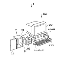
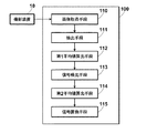
以下、図面を参照して本発明の蛍光検出装置および画像処理システムの実施の形態を詳細に説明する。図1は本発明の画像処理システムの一例を示す斜視図である。図1の画像処理システム1はたとえば蛍光標識物を被写体として、被写体に励起光を照射することにより蛍光画像を表示する画像処理システムであって、蛍光検出装置10と画像処理装置100とを有する。蛍光検出装置10および画像処理装置100は机上に配置されるものであって、画像処理装置100はたとえばパーソナルコンピュータからなっており、マウスやキーボード等の入力手段2およびCRTや液晶ディスプレイ等からなる表示部3に接続されている。そして、蛍光検出装置10が蛍光標識物PSを撮影して、取得した蛍光標識物の画像情報を画像処理装置100に送り、画像処理装置100が画像情報を画像処理して表示部3で表示するようになっている。
Embodiments of a fluorescence detection apparatus and an image processing system according to the present invention will be described below in detail with reference to the drawings. FIG. 1 is a perspective view showing an example of an image processing system of the present invention. An
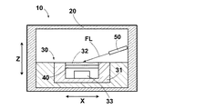
図2は本発明の蛍光検出装置の好ましい実施の形態を示す模式図である。図2の蛍光検出装置10は、蛍光標識物PSを内部に収容した筐体20と、筐体20内に配置された蛍光標識物PSに励起光FLを照射する励起光源50と、励起光源50からの励起光FLの照射により蛍光標識物PSが射出する蛍光を撮像して画像情報を出力する撮像デバイス30とを備えている。
FIG. 2 is a schematic diagram showing a preferred embodiment of the fluorescence detection apparatus of the present invention. The
ここで、筐体20は略直方体に形成された中空部21を有するものであって、開閉可能な蓋22を有している。そして、ユーザーが蓋22を開けて筐体20内に蛍光標識物PSを収容することができるようになっている。このように、筐体20は中空部21内に外光が入らないような暗箱を構成しており、蛍光標識物PSから微弱光が射出された場合であっても撮影が可能になっている。なお、蛍光標識物PSとは、たとえばホルモン類、腫瘍マーカー、酵素、抗体、抗原、アブザイム、その他の蛋白質、核酸、cDNA、DNA、mRNAなどの物質を蛍光色素によって標識されたものをいう。
Here, the housing | casing 20 has the
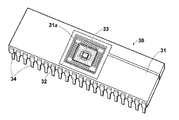
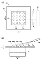
撮像デバイス30は筐体20の下側に固定された、たとえば特表2001−511887号公報に示すような半導体パッケージからなっており、撮像素子33と、撮像素子33上に設けられた、蛍光標識物PSが配置される光透過板32とを有している。具体的には、図3に示すように、撮像デバイス30は、撮像素子33を収容した、撮像素子33上に開口部31aを有するモールド部31と、開口部31aに固定された、蛍光標識物PSが配置される光透過板32と、撮像素子33により取得された画像情報を外部に出力する外部端子34とを備えている。そして、この撮像デバイス30には、図4(a)に示すように、光透過板32上における撮像素子33の撮像可能領域内に複数の蛍光標識物PSがたとえば格子状に複数配置されるようになっている。
The
励起光源50は、格子状に配列された蛍光標識物PSにそれぞれ励起光FLを照射するため、たとえば矢印Y方向に複数の発光素子を配列したライン状の励起光FLを矢印X方向に走査するようになっている。なお、励起光源50は、スポット状の励起光FLを矢印
X方向および矢印Y方向に走査させることにより、複数の蛍光標識物PSに励起光FLを照射するものであってもよい。
The
ここで、励起光源50は、蛍光標識物PSに光透過板32の全反射角よりも浅い角度θcから励起光FLを照射するようになっている。具体的には、励起光源50は、図4(b)に示すように、励起光源50に最も近い蛍光標識物PS1が配置されている位置への励起光FLの入射角が光透過板32の全反射角よりも浅い角度θcになるように設置されている。すると、励起光FLが矢印X1方向に走査されるにつれて励起光FLの光透過板32への入射角θcは小さくなっていくため、励起光FLは光透過板32において常に全反射されることになる。これにより、励起光FLが撮像素子33に入射するのを防止することができるため、励起光FLを照射しなければ検査ができないような蛍光標識物PSについても、図3および図4に示すような、撮像素子33と蛍光標識物PSとをほぼ密着させる撮像デバイス30を使用することができるため、蛍光標識物PSの高精度な分析を行うことができる。
Here, the
さらに、励起光FLを光透過板33の全反射角よりも浅い角度θcから照射するだけでなく、図2に示すように、光透過板32の表面に、励起光FLを遮光し蛍光を透過する分光フィルタ40を設けるようにしてもよい。これにより、撮像素子33に励起光FLが入射するのを確実に防止することができる。なお、図2においては、分光フィルタ40が光透過板32の撮像素子33側に設けられている場合について例示しているが、励起光源側50に設けられていてもよい。
Further, not only the excitation light FL is irradiated from an angle θc shallower than the total reflection angle of the
図5は本発明の画像処理システム1に使用される画像処理装置100の好ましい実施の形態を示すブロック図であり、図1から図5を参照して画像処理装置100について説明する。図5の画像処理装置100は、上述した蛍光検出装置10により取得された画像情報を処理する画像処理装置100を有するものであって、撮像素子33が光透過板32に配置された蛍光標識物PSを撮影したときに、撮像素子33の各画素から画素信号を取得する信号取得手段110と、信号取得手段110により取得された複数の画素信号の中から、同一の蛍光標識物PSを撮像した複数の画素からそれぞれ取得した画素信号を抽出する信号抽出手段111と、信号抽出手段111により抽出された複数の画素信号の第1平均値を算出する第1平均値算出手段112と、信号抽出手段111により抽出された複数の画素信号の中から、第1平均値算出手112段により算出された平均値から所定のしきい値以上離れている異常画素信号を検出する信号検出手段113と、信号抽出手段111により抽出された複数の画素信号のうち、信号検出手段113により検出された異常画素信号を除いた画素信号の第2平均値を算出する第2平均値算出手段114と、信号抽出手段111により抽出された複数の画素信号を第2平均値算出手段により算出された第2平均値に置換する信号置換手段115とを有する。
FIG. 5 is a block diagram showing a preferred embodiment of the
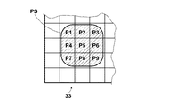
具体的には、たとえば蛍光標識物PSの径はたとえば75μm〜300μmであり、撮像素子33の画素はたとえば50μm×50μmであるとき、図6に示すように、撮像素子33の複数の画素P1〜P9が同一の蛍光標識物PSを撮像するようになる。ここで、信号取得手段110が、撮像素子33のすべての画素(画素P1〜P9を含む)から画素信号を取得したとき、信号抽出手段111が、信号取得手段110により取得された複数の画素信号の中から、同一の蛍光標識物PSを撮像した複数の画素P1〜P9が取得した画素信号を抽出するようになっている。
Specifically, for example, when the diameter of the fluorescent label PS is 75 μm to 300 μm and the pixels of the
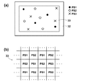
なお、信号抽出手段111が複数の画素P1〜P9を抽出する際、予め蛍光標識物PSの配置位置がわかっており、その配置位置に対応した画素の画素信号を抽出するようにしてもよいし、画像情報のエッジ検出をすることにより、各蛍光標識物PS毎にそれを撮像した複数の画素を検出するようにしてもよい。また、図6においては説明の容易のため、蛍光標識物PSが画素P1〜P9に凝集している場合について例示しているが、信号抽出手段111は、同一の蛍光標識物PSを撮像した画素の画素信号を各蛍光標識物PS毎に抽出するものであればよい。たとえば、図7(a)に示すように、光透過板32上に複数の蛍光標識物PS1、PS2、PS3がランダムに存在しているとき、信号抽出手段111は、各蛍光標識物PS1〜PS3毎にそれぞれ撮像素子33の画素の画素信号を抽出するものであってもよい。また、図7(b)に示すように、たとえば3つの蛍光標識物PS1〜PS3が光透過板32上に千鳥状に存在する場合であっても、信号抽出手段111は、信号抽出手段111は、各蛍光標識物PS1〜PS3毎にそれぞれ撮像素子33の画素の画素信号を抽出するものであってもよい。
When the
なお、図7(a)、(b)においては3種類の蛍光標識物PS1〜PS3が存在している場合について例示しているが、3種類以上複数の蛍光標識物が光透過板32上に存在する場合についても適用することができる。この場合であっても、各蛍光標識物毎に画素信号が抽出されるようになる。
7A and 7B exemplify the case where three types of fluorescent labels PS1 to PS3 exist, three or more types of fluorescent labels are present on the
第1平均値算出手段112は、信号抽出手段111により抽出された画素P1〜P9の画素信号の平均値を算出する。そして、信号検出手段113は、信号抽出手段111により抽出された画素P1〜P9の画素信号の中から、第1平均値算出手段112により算出された平均値から所定のしきい値以上離れている異常画素信号を検出する。ここで、所定のしきい値にはたとえば±2σ(σは画素P1〜P9の画素信号のばらつき)が用いられる。ここでは、図6の画素P5が欠陥画素であって、画素P5から取得される画素信号が異常画素信号であるとする。このとき、第2平均値算出手段114は、信号検出手段113により検出された異常画素信号(画素P5の画素信号)を除いた画素P1〜P9の画素信号の平均値を算出する。その後、信号置換手段115が画素P1〜P9の画素信号を第2平均値算出手段114により算出された第2平均値に置換する。すなわち、画素P1〜P9により撮像された蛍光標識物PSを示す画像情報として第2平均値の信号値が用いられる。
The first average
これにより、撮像素子33にたとえば画素欠陥が存在し、もしくは他の画素と感度特性の異なる画素が存在する場合であっても、その不良画素等が撮像した蛍光標識物を撮像した他の画素の画素信号を用いて不良画素の画素信号を補間することができる。
As a result, even if, for example, a pixel defect exists in the
なお、第1平均値算出手段112、信号検出手段113、第2平均値算出手段113および信号置換手段115において、図7(a)、(b)のように、複数の蛍光標識物PS1〜PS3毎に複数の画素信号が分類されている場合には、各蛍光標識物PS1〜PS3毎にそれぞれ第1平均値の算出、異常画素信号の検出、第2平均値の算出および画素信号の置換が行われる。 In the first average value calculating means 112, the signal detecting means 113, the second average value calculating means 113, and the signal replacing means 115, as shown in FIGS. 7A and 7B, a plurality of fluorescent labels PS1 to PS3 are used. When a plurality of pixel signals are classified for each, the calculation of the first average value, the detection of the abnormal pixel signal, the calculation of the second average value, and the replacement of the pixel signal are performed for each fluorescent marker PS1 to PS3. Done.
上記実施の形態によれば、撮像デバイス30が、撮像素子を収容した、撮像素子上に開口部を有するモールド部と、開口部31aに固定された、蛍光標識物PSが配置される光透過板32とを有し、励起光源50が、蛍光標識物に光透過板32の全反射角よりも浅い角度θcから励起光FLを照射するものであることにより、撮像素子33と蛍光標識物PSとを密着させて蛍光検出を行ったときに、蛍光標識物PSに照射される励起光FLは光透過板32により全反射されるため、撮像素子に励起光が入射されるのを防止して高感度な蛍光検出を行うことができる。
According to the above-described embodiment, the
また、図3のように、光透過板32の表面に、励起光FLを遮光し蛍光を透過する分光フィルタが設けられている構成で有れば、励起光FLが撮像素子33に入射するのを確実に防止することができる。
Further, as shown in FIG. 3, if the spectral filter that blocks the excitation light FL and transmits the fluorescence is provided on the surface of the
また、図5の画像処理装置100を用いた画像処理システム1によれば、画像処理装置100が、撮像素子33が光透過板32に配置された複数の蛍光標識物PSを撮影したときに、撮像素子33の各画素から画素信号を取得する信号取得手段110と、信号取得手段110により取得された複数の画素信号の中から、同一の蛍光標識物PSを撮像した複数の画素がそれぞれ取得した画素信号を抽出する信号抽出手段111と、信号抽出手段111により抽出された複数の画素信号の平均値を算出する第1平均値算出手段112と、信号抽出手段111により抽出された複数の画素信号の中から、第1平均値算出手段112により算出された平均値から所定のしきい値以上離れている画素信号を検出する信号検出手段113と、信号検出手段113により検出された画素信号を除いた複数の画素信号の平均値を算出する第2平均値算出手段114と、信号抽出手段111により抽出された複数の画素信号を第2平均値算出手段114により算出された平均値に置換する信号置換手段115とを有するものであることにより、撮像素子33に不良画素が存在する場合であっても、その不良画素と同一の蛍光標識物PSを撮影した画素の画素信号を用いて不良画素の画素信号を補間することができる。
Further, according to the
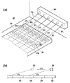
なお、本発明の実施の形態は、上記実施の形態に限定されない。たとえば、図2から図6において、蛍光検出装置10は、1つの撮像デバイス30を有する場合について例示しているが、図8(a)に示すように、複数の撮像デバイス30が格子状に配列しているものであってもよいし、複数の撮像デバイス30がライン状に配列されたものであってもよい。このとき、図4と同様に、励起光源50が、励起光源50に最も近い撮像デバイス列20aが配置されている位置への励起光FLの入射角が光透過板32の全反射角よりも浅い角度θcになるように設置されており、励起光FLが矢印X1方向に走査していけば、すべての撮像デバイス30において、励起光FLは光透過板32において常に全反射されることになる。これにより、撮像素子33と蛍光標識物PSとを密着させて蛍光検出を行ったときであっても、蛍光標識物PSに照射される励起光は光透過板により全反射されるため、撮像素子33に励起光FLが入射されるのを防止して高感度な蛍光検出を行うことができる。
The embodiment of the present invention is not limited to the above embodiment. For example, in FIGS. 2 to 6, the
さらに、図4および図8(a)においては、励起光源50は固定されており、励起光源50から射出する励起光FLが走査する場合について例示しているが、図8(b)に示すように、励起光源50自体が矢印X1方向に走査することにより、複数の撮像素子33(蛍光標識物PS)に励起光FLを照射するようにしてもよい。これにより、各蛍光標識物PSに同一の入射角θcで励起光FLを照射することができるため、複数の蛍光標識物PSに対して同一の実験条件下における蛍光検出を行うことができる。
Further, FIGS. 4 and 8A illustrate the case where the
1 画像処理システム
10 蛍光検出装置
20 筐体
21 中空部
30 撮像デバイス
31 モールド部
31a 開口部
32 光透過板
33 撮像素子
34 外部端子
40 分光フィルタ
50 励起光源
100 画像処理装置
110 信号取得手段
111 信号抽出手段
112 第1平均値算出手段
113 信号検出手段
114 第2平均値算出手段
115 信号置換手段
FL 励起光
P1〜P9 画素
PS 蛍光標識物
DESCRIPTION OF
Claims (3)
該撮像デバイスが、撮像素子と、該撮像素子上に設けられた、前記蛍光標識物が配置される光透過板とを有し、
前記励起光源が、前記蛍光標識物に前記光透過板の全反射角よりも浅い角度から前記励起光を照射するものであることを特徴とする蛍光検出装置。 A casing that accommodates the fluorescent label, an excitation light source that irradiates the fluorescent label disposed in the casing with excitation light, and the fluorescent label is emitted by irradiation of the excitation light from the excitation light source An imaging device that captures fluorescence to acquire image information,
The imaging device includes an imaging element, and a light transmission plate provided on the imaging element, on which the fluorescent label is disposed,
The fluorescence detection apparatus, wherein the excitation light source irradiates the excitation light from an angle shallower than a total reflection angle of the light transmission plate on the fluorescent label.
該撮像デバイスが、撮像素子と、該撮像素子上に設けられた、前記蛍光標識物が配置される光透過板とを有し、
前記励起光源が、前記蛍光標識物に前記光透過板の全反射角よりも浅い角度から前記励起光を照射するものであって、
前記画像処理装置が、
前記撮像素子が前記光透過板に配置された前記蛍光標識物を撮影したときに、前記撮像素子の各画素から画素信号を取得する信号取得手段と、
該信号取得手段により取得された複数の前記画素信号の中から、同一の前記蛍光標識物を撮像した前記複数の画素からそれぞれ取得した画素信号を抽出する信号抽出手段と、
該信号抽出手段により抽出された複数の前記画素信号の第1平均値を算出する第1平均値算出手段と、
前記信号抽出手段により抽出された複数の前記画素信号の中から、前記第1平均値算出手段により算出された平均値から所定のしきい値以上離れている異常画素信号を検出する信号検出手段と、
前記信号抽出手段により抽出された複数の前記画素信号のうち、前記信号検出手段により検出された前記異常画素信号を除いた前記画素信号の第2平均値を算出する第2平均値算出手段と、
前記信号抽出手段により抽出された複数の前記画素信号を前記第2平均値算出手段により算出された第2平均値に置換する信号置換手段と
を有するものであることを特徴とする画像処理システム。 A casing that accommodates the fluorescent label, an excitation light source that irradiates the fluorescent label disposed in the casing with excitation light, and the fluorescent label is emitted by irradiation of the excitation light from the excitation light source In an image processing system having a fluorescence detection device including an imaging device that captures fluorescence and outputs image information, and an image processing device that processes image information acquired by the fluorescence detection device,
The imaging device includes an imaging element, and a light transmission plate provided on the imaging element, on which the fluorescent label is disposed,
The excitation light source irradiates the excitation light from an angle shallower than the total reflection angle of the light transmission plate on the fluorescent label;
The image processing apparatus is
Signal acquisition means for acquiring a pixel signal from each pixel of the image sensor when the image sensor images the fluorescent label placed on the light transmission plate;
Signal extraction means for extracting pixel signals respectively acquired from the plurality of pixels obtained by imaging the same fluorescent marker from the plurality of pixel signals acquired by the signal acquisition means;
First average value calculating means for calculating a first average value of the plurality of pixel signals extracted by the signal extracting means;
Signal detecting means for detecting an abnormal pixel signal that is more than a predetermined threshold from the average value calculated by the first average value calculating means from among the plurality of pixel signals extracted by the signal extracting means; ,
A second average value calculating means for calculating a second average value of the pixel signals excluding the abnormal pixel signal detected by the signal detecting means among the plurality of pixel signals extracted by the signal extracting means;
An image processing system comprising: a signal replacement unit that replaces the plurality of pixel signals extracted by the signal extraction unit with a second average value calculated by the second average value calculation unit.
Priority Applications (1)
| Application Number | Priority Date | Filing Date | Title |
|---|---|---|---|
| JP2004104254A JP2005291795A (en) | 2004-03-31 | 2004-03-31 | Fluorescence detection device and image processing system |
Applications Claiming Priority (1)
| Application Number | Priority Date | Filing Date | Title |
|---|---|---|---|
| JP2004104254A JP2005291795A (en) | 2004-03-31 | 2004-03-31 | Fluorescence detection device and image processing system |
Publications (1)
| Publication Number | Publication Date |
|---|---|
| JP2005291795A true JP2005291795A (en) | 2005-10-20 |
Family
ID=35324902
Family Applications (1)
| Application Number | Title | Priority Date | Filing Date |
|---|---|---|---|
| JP2004104254A Withdrawn JP2005291795A (en) | 2004-03-31 | 2004-03-31 | Fluorescence detection device and image processing system |
Country Status (1)
| Country | Link |
|---|---|
| JP (1) | JP2005291795A (en) |
Cited By (6)
| Publication number | Priority date | Publication date | Assignee | Title |
|---|---|---|---|---|
| JP2007322185A (en) * | 2006-05-31 | 2007-12-13 | Hitachi High-Technologies Corp | Fluorescence analysis method, fluorescence analysis apparatus and image detection method |
| JP2008039564A (en) * | 2006-08-04 | 2008-02-21 | Canon Inc | Inspection device |
| JP2009180740A (en) * | 2009-05-11 | 2009-08-13 | Hitachi High-Technologies Corp | Fluorescence analysis method, fluorescence analysis apparatus and image detection method |
| WO2018105607A1 (en) * | 2016-12-09 | 2018-06-14 | コニカミノルタ株式会社 | Measuring device, measurement abnormality detecting method, and program |
| CN110823856A (en) * | 2019-12-19 | 2020-02-21 | 北京永安多谱检测科技有限公司 | Excited fluorescence peroxide detection device based on image analysis and detection method thereof |
| JP2023087434A (en) * | 2021-12-13 | 2023-06-23 | Tdk株式会社 | Program, information processing device, information processing method, and information processing system |
-
2004
- 2004-03-31 JP JP2004104254A patent/JP2005291795A/en not_active Withdrawn
Cited By (11)
| Publication number | Priority date | Publication date | Assignee | Title |
|---|---|---|---|---|
| JP2007322185A (en) * | 2006-05-31 | 2007-12-13 | Hitachi High-Technologies Corp | Fluorescence analysis method, fluorescence analysis apparatus and image detection method |
| JP2008039564A (en) * | 2006-08-04 | 2008-02-21 | Canon Inc | Inspection device |
| JP2009180740A (en) * | 2009-05-11 | 2009-08-13 | Hitachi High-Technologies Corp | Fluorescence analysis method, fluorescence analysis apparatus and image detection method |
| WO2018105607A1 (en) * | 2016-12-09 | 2018-06-14 | コニカミノルタ株式会社 | Measuring device, measurement abnormality detecting method, and program |
| JPWO2018105607A1 (en) * | 2016-12-09 | 2019-10-24 | コニカミノルタ株式会社 | Measurement apparatus, measurement abnormality detection method, and program |
| JP7034087B2 (en) | 2016-12-09 | 2022-03-11 | 大塚製薬株式会社 | Measuring equipment, measurement anomaly detection method, and program |
| US11397150B2 (en) | 2016-12-09 | 2022-07-26 | Otsuka Pharmaceutical Co., Ltd. | Measuring device, measurement abnormality detecting method, and program |
| CN110823856A (en) * | 2019-12-19 | 2020-02-21 | 北京永安多谱检测科技有限公司 | Excited fluorescence peroxide detection device based on image analysis and detection method thereof |
| CN110823856B (en) * | 2019-12-19 | 2024-06-07 | 北京永安多谱检测科技有限公司 | Excited fluorescent peroxide detection device based on image analysis and detection method thereof |
| JP2023087434A (en) * | 2021-12-13 | 2023-06-23 | Tdk株式会社 | Program, information processing device, information processing method, and information processing system |
| US12512919B2 (en) | 2021-12-13 | 2025-12-30 | Tdk Corporation | Non-transitory computer readable storage medium, information processing device, information processing method, and information processing system |
Similar Documents
| Publication | Publication Date | Title |
|---|---|---|
| US7199357B1 (en) | Image enhancement by sub-pixel imaging | |
| CN103339493B (en) | Analysis method and reading device for microarray | |
| US7680316B2 (en) | Imaging device and methods to derive an image on a solid phase | |
| CN101836114A (en) | Immunoassay analysis method | |
| JP7830346B2 (en) | Aggregation-induced assay for enhanced sensitivity | |
| JP4979516B2 (en) | Image reading method and apparatus | |
| CN101592654A (en) | Image analysis method of biodetector | |
| US20090292479A1 (en) | Method for analyzing image from bio-detection analyzer | |
| GB2515490A (en) | An aperture array substrate device, a detection system and a method for detecting analytes in a sample | |
| JP2005291795A (en) | Fluorescence detection device and image processing system | |
| JP3929057B2 (en) | Luminescence intensity analysis method and apparatus | |
| TW200944777A (en) | Method for analyzing image from bio-detection analyzer | |
| KR102048599B1 (en) | Determination method, determination device, determination system, and program | |
| KR101263800B1 (en) | Bio-chip detector | |
| CA2450385C (en) | Flat field correction of two-dimensional biochemical assay images | |
| EP1845366A8 (en) | Analysis processing method and device | |
| EP1688744A1 (en) | Biological information inspection system | |
| JP2000338042A (en) | Method and apparatus for filing image data | |
| CN1508266A (en) | Biochip Detection System | |
| JP2007309886A (en) | Analyzer | |
| EP2885244B1 (en) | Protein specific optical detection | |
| RU200805U1 (en) | Fluorescent Biochip Analyzer | |
| CN102171568A (en) | Method for detecting analytes in a sample microarray and device for carrying out said method | |
| JP2019052932A (en) | Data analyzer, program and recording medium, and data analysis method | |
| US20200056995A1 (en) | Biological substance analysis method, biological substance analyzer, biological substance analysis program, and biological substance analysis system |
Legal Events
| Date | Code | Title | Description |
|---|---|---|---|
| A300 | Withdrawal of application because of no request for examination |
Free format text: JAPANESE INTERMEDIATE CODE: A300 Effective date: 20070605 |