JP2005291728A - Goniometer with giant magnetoresistive element - Google Patents
Goniometer with giant magnetoresistive element Download PDFInfo
- Publication number
- JP2005291728A JP2005291728A JP2004102764A JP2004102764A JP2005291728A JP 2005291728 A JP2005291728 A JP 2005291728A JP 2004102764 A JP2004102764 A JP 2004102764A JP 2004102764 A JP2004102764 A JP 2004102764A JP 2005291728 A JP2005291728 A JP 2005291728A
- Authority
- JP
- Japan
- Prior art keywords
- giant magnetoresistive
- magnetoresistive element
- magnetic field
- planar coil
- pairs
- Prior art date
- Legal status (The legal status is an assumption and is not a legal conclusion. Google has not performed a legal analysis and makes no representation as to the accuracy of the status listed.)
- Granted
Links
- 238000005259 measurement Methods 0.000 claims abstract description 8
- 230000005291 magnetic effect Effects 0.000 claims description 111
- 230000005415 magnetization Effects 0.000 claims description 15
- 230000005294 ferromagnetic effect Effects 0.000 claims description 13
- 239000010409 thin film Substances 0.000 claims description 9
- 238000004519 manufacturing process Methods 0.000 abstract description 3
- 238000010586 diagram Methods 0.000 description 8
- 239000000758 substrate Substances 0.000 description 5
- 239000010408 film Substances 0.000 description 4
- 230000035945 sensitivity Effects 0.000 description 4
- 239000013078 crystal Substances 0.000 description 2
- 230000007423 decrease Effects 0.000 description 2
- 238000000034 method Methods 0.000 description 2
- 229920006395 saturated elastomer Polymers 0.000 description 2
- 229910018072 Al 2 O 3 Inorganic materials 0.000 description 1
- 239000000956 alloy Substances 0.000 description 1
- 229910045601 alloy Inorganic materials 0.000 description 1
- 230000002457 bidirectional effect Effects 0.000 description 1
- 230000003247 decreasing effect Effects 0.000 description 1
- 230000020169 heat generation Effects 0.000 description 1
- 239000000463 material Substances 0.000 description 1
Images


Landscapes
- Measuring Magnetic Variables (AREA)
Abstract
Description
本発明は等方性の巨大磁気抵抗素子を用いた方位計、特に巨大磁気抵抗素子にバイアス磁界を印加しながら方位を測定する方位計に関するものである。 The present invention relates to an azimuth meter using an isotropic giant magnetoresistive element, and more particularly to an azimuth meter that measures an azimuth while applying a bias magnetic field to the giant magnetoresistive element.
本出願人は異方性磁気抵抗素子と平面コイルとを組み合わせた方位計を既に出願しており、特許文献1として公開されている。特許文献1の方位計は図9に分解斜視図で示すように、ほぼ方形をした平面コイル1と、平面コイルに平行で近接した平面に8個の磁気抵抗素子61,62,71,72,81,82,91,92を持っている。2個の磁気抵抗素子(例えば、61,72)が平面コイルの各辺(例えば、11)とそれら磁気抵抗素子の長手方向とほぼ45°で交差しており、それら2個の磁気抵抗素子の長手方向は互いに直角となっている。そして平面コイルの対向している2辺(例えば、11と12)のそれぞれと交差しており、互いに長手方向が直角となっている2個の磁気抵抗素子(例えば、61と62、71と72)によって磁気抵抗素子対6,7,8,9を形成している。磁気抵抗素子対(例えば、6)の一方の端部同士が接続されていて、磁気抵抗素子対(例えば、6)の他の端部間に測定用電圧Vccが印加される。平面コイルによって磁気抵抗素子対にバイアス磁界を印加している間に、磁気抵抗素子対6,7,8,9の接続されている端部から磁気抵抗素子対の中間電圧を取り出し、平面コイル1の対向している2辺11と12と交差している2組の磁気抵抗素子対6と7の中間電圧差Vxを求める。平面コイル1の対向している他の2辺13と14と交差している他の2組の磁気抵抗素子対8、9についても同様に中間電圧差Vyを求める。次に平面コイル1によって磁気抵抗素子対6,7,8,9に反対方向のバイアス磁界を印加している間に、同様に平面コイル1の対向している2辺11と12と交差している2組の磁気抵抗素子対6、7の中間電圧差Vxを求め、平面コイル1の対向している他の2辺13と14と交差している他の2組の磁気抵抗素子対8、9についても同様に中間電圧差Vyを求める。そして、平面コイルの一方の対向している2辺11,12と交差している2組の磁気抵抗素子対6,7について、先に印加したバイアス磁界をかけているときに求めた中間電圧差Vxと、反対方向バイアス磁界をかけているときに求めた中間電圧差Vxとの差電圧を求め、平面コイルの他の対向している2辺13,14と交差している2組の磁気抵抗素子対8,9について、先に印加したバイアス磁界をかけているときに求めた中間電圧差Vyと、反対方向バイアス磁界をかけているときに求めた中間電圧差Vyとの差電圧を求める。そしてこれら2個の差電圧の比から外部磁界(例えば、地磁気)の方向を求めるようになっている。
The present applicant has already applied for an azimuth meter in which an anisotropic magnetoresistive element and a planar coil are combined, and is disclosed as Patent Document 1. As shown in an exploded perspective view of FIG. 9, the compass of Patent Document 1 includes a substantially rectangular planar coil 1 and eight
磁気抵抗素子は、電流の流す方向と直角方向に印加した磁界の強さに応じて電流に対する抵抗が変化し、電流と直角な磁界が強くなるに従って抵抗が小さくなる。方位計として用いる場合、各磁気抵抗素子の抵抗変化率がほぼ同一であることが望ましく、そのために上で説明した方位計の各磁気抵抗素子は長手方向に結晶磁気異方性を付けている。
特許文献1に示されている方位計では図9に示すように、4個の磁気抵抗素子61,71,81,91と4個の磁気抵抗素子62,72,82,92とはそれらの長手方向が互いに垂直となっている。これら8個の磁気抵抗素子にそれぞれの長手方向に結晶磁気異方性を付けるには、同じ方向の4個の磁気抵抗素子61,71,81,91をそれらの長手方向に磁界を印加しながら形成し、その後でそれらと垂直な4個の磁気抵抗素子62,72,82,92をそれらの長手方向に磁界を印加しながら形成する必要があった。
In the compass shown in Patent Document 1, as shown in FIG. 9, the four
また、磁気抵抗素子の幅方向にかかる外部磁界(地磁気等)を検出するので、幅方向寸法を小さくするとその反磁界の影響が大きくなって地磁気のように弱い磁界の測定には感度が悪くなるものであった。そこである程度の幅寸法を持った磁気抵抗素子にせざるを得なかったが、幅寸法を大きくすると磁気抵抗素子の抵抗が小さくなるので、測定用電圧を磁気抵抗素子対にかけたときの消費電力が大きくなっていた。そこで磁気抵抗素子の抵抗を上げるには磁気抵抗素子を長くすることになるが、磁気抵抗素子幅を広く、長さを長くすると磁気抵抗素子面積が大きくなるので、方位計を大きくする必要があった。 Also, since an external magnetic field (such as geomagnetism) applied in the width direction of the magnetoresistive element is detected, the influence of the demagnetizing field increases when the width dimension is reduced, and the sensitivity is poor for measurement of weak magnetic fields such as geomagnetism. It was a thing. Therefore, it was necessary to use a magnetoresistive element having a certain width. However, if the width is increased, the resistance of the magnetoresistive element is reduced, so that the power consumption when applying the measurement voltage to the magnetoresistive element pair is large. It was. In order to increase the resistance of the magnetoresistive element, the magnetoresistive element is lengthened. However, if the width of the magnetoresistive element is wide and the length is increased, the area of the magnetoresistive element is increased. It was.
そこで、本発明では上記欠点を改善するために、等方性の巨大磁気抵抗素子を用いた方位計を提供するものである。 Therefore, the present invention provides an azimuth meter using an isotropic giant magnetoresistive element in order to improve the above drawbacks.
本発明の方位計は、互いに平行となっている対辺対を少なくとも部分的に有する平面コイルと、
その平面コイル面の同じ側にあって、平面コイル面に平行で近接した平面内に設けられた巨大磁気抵抗素子2個からなる少なくとも1組の巨大磁気抵抗素子対とを有しており、
巨大磁気抵抗素子それぞれは、強磁性層と非磁性層とを交互に積層した積層薄膜であり、その長手方向寸法に対して薄膜の幅方向寸法が十分に小さな形状をしており、
巨大磁気抵抗素子対の各巨大磁気抵抗素子の長手方向は平面コイルの対辺対の各1辺のみと実質的に直交しており、
巨大磁気抵抗素子対の巨大磁気抵抗素子の一方の端部同士が接続されているとともに、他方の端部間に測定用電圧が印加されるようになっており、一方の端部から中間電圧を取り出すようになっている。
The compass of the present invention comprises a planar coil having at least part of opposite side pairs that are parallel to each other;
Having at least one giant magnetoresistive element pair consisting of two giant magnetoresistive elements provided in a plane parallel to and close to the planar coil surface on the same side of the planar coil surface;
Each giant magnetoresistive element is a laminated thin film in which ferromagnetic layers and nonmagnetic layers are alternately laminated, and the width direction dimension of the thin film is sufficiently small with respect to its longitudinal dimension,
The longitudinal direction of each giant magnetoresistive element of the giant magnetoresistive element pair is substantially perpendicular to only one side of the opposite side pair of the planar coil,
One end of the giant magnetoresistive element of the giant magnetoresistive element pair is connected to each other, and a measurement voltage is applied between the other end, and an intermediate voltage is applied from one end. It comes to take out.
本発明の方位計は、巨大磁気抵抗素子対を2組持ち、平面コイルは巨大磁気抵抗素子対の各組と交差している対辺対を2組持っているとともに、その2組の対辺対が互いに垂直であることが好ましい。 The compass of the present invention has two pairs of giant magnetoresistive elements, and the planar coil has two pairs of opposite sides that intersect with each pair of giant magnetoresistive elements, and the two opposite pairs are Preferably they are perpendicular to each other.
本発明の方位計は、巨大磁気抵抗素子対を4組持ち、平面コイルは巨大磁気抵抗素子対の各2組と交差している対辺対を2組持っているとともに、その2組の対辺対が互いに垂直であることが更に好ましい。 The compass of the present invention has four pairs of giant magnetoresistive elements, and the planar coil has two pairs of opposite sides that intersect each two pairs of giant magnetoresistive elements, and the two pairs of opposite sides. More preferably, are perpendicular to each other.
本発明の方位計は、更に平面コイルに電流を供給するための電源を更に持っており、その電源は、巨大磁気抵抗素子の磁化が長手方向に飽和する大きさの直流磁界を巨大磁気抵抗素子に印加するのに十分な直流電流を平面コイルに供給し、
巨大磁気抵抗素子に前にかけた直流磁界よりも小さな所定の直流磁界を印加する直流電流を平面コイルに供給し、
巨大磁気抵抗素子の磁化が前とは逆方向に飽和する大きさの直流磁界を巨大磁気抵抗素子に印加するのに十分な直流電流を平面コイルに供給し、そして
巨大磁気抵抗素子に前回の所定の直流磁界と逆方向の所定の直流磁界を印加する直流電流を平面コイルに供給するものであることが好ましい。
The azimuth meter of the present invention further has a power source for supplying a current to the planar coil, and the power source generates a DC magnetic field having a magnitude that saturates the magnetization of the giant magnetoresistive element in the longitudinal direction. Sufficient DC current to be applied to the planar coil,
A DC current that applies a predetermined DC magnetic field smaller than the DC magnetic field previously applied to the giant magnetoresistive element is supplied to the planar coil,
Sufficient DC current is applied to the giant magnetoresistive element to apply a DC magnetic field with a magnitude that saturates in the opposite direction to the magnetization of the giant magnetoresistive element. It is preferable that a DC current for applying a predetermined DC magnetic field in a direction opposite to the DC magnetic field is supplied to the planar coil.
本発明の方位計において、巨大磁気抵抗素子に最初の所定の直流磁界を印加している間に各巨大磁気抵抗素子対の一方の端部から第一の中間電圧を取り出し、
巨大磁気抵抗素子に最初とは逆方向の所定の直流磁界を印加している間に各巨大磁気抵抗素子対の一方の端部から第二の中間電圧を取り出し、
第一と第二の中間電圧の差に基づいて外部磁界の方位を求める演算器を有していることが好ましい。
In the azimuth meter of the present invention, the first intermediate voltage is taken out from one end of each giant magnetoresistive element pair while applying the first predetermined DC magnetic field to the giant magnetoresistive element,
While applying a predetermined DC magnetic field in the opposite direction to the first to the giant magnetoresistive element, a second intermediate voltage is taken out from one end of each giant magnetoresistive pair,
It is preferable to have an arithmetic unit that obtains the direction of the external magnetic field based on the difference between the first and second intermediate voltages.
本発明の等方性巨大磁気抵抗素子を用いた方位計は、巨大磁気抵抗素子を形成する際に結晶磁気異方性を制御する必要がないから、製造工程が単純になって製造が容易である。 Since the azimuth meter using the isotropic giant magnetoresistive element of the present invention does not need to control the magnetocrystalline anisotropy when forming the giant magnetoresistive element, the production process is simplified and the manufacture is easy. is there.
また、本発明では等方性巨大磁気抵抗素子の幅方向の反磁界を利用しているので、幅寸法をできるだけ小さくすることが好ましく、方位計の小型化、低消費電力とすることができる。 In the present invention, since the demagnetizing field in the width direction of the isotropic giant magnetoresistive element is used, it is preferable to make the width dimension as small as possible, and the direction meter can be downsized and the power consumption can be reduced.
更に、巨大磁気抵抗素子の幅寸法を小さくしているので、測定すべき磁界の巨大磁気抵抗素子の幅方向成分による影響を小さくすることができる。 Furthermore, since the width dimension of the giant magnetoresistive element is reduced, the influence of the magnetic field to be measured due to the width direction component of the giant magnetoresistive element can be reduced.
このような利点を本発明の方位計は持っていて、しかも外部磁界の印加された方向を測定することができる。 The compass of the present invention has such advantages, and can measure the direction in which an external magnetic field is applied.
また、地磁気以外の磁界発生源より発せられる磁界方向と巨大磁気抵抗素子の感軸方向とがなす角を測定する、角度センサーとしても用いることができる。 It can also be used as an angle sensor for measuring the angle formed by the direction of a magnetic field generated from a magnetic field generation source other than geomagnetism and the sensitive axis direction of the giant magnetoresistive element.
実施例1
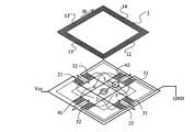
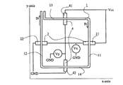
本発明の実施例1の方位計を分解斜視図で図1に、またその回路図を図2に示している。図1、図2で1は平行四辺形状(ここでは正方形)をした平面コイルで数十回巻かれている。この平面コイル面の同じ側に、この図では下側に、この平面コイル面に平行で近接した平面内に巨大磁気抵抗素子対2,3,4,5が4組設けられている。巨大磁気抵抗素子対2,3,4,5それぞれは2個の巨大磁気抵抗素子21と22,31と32,41と42,51と52からなっている。
Example 1
FIG. 1 is an exploded perspective view of the compass of the first embodiment of the present invention, and FIG. 2 is a circuit diagram thereof. 1 and 2, reference numeral 1 denotes a flat coil having a parallelogram shape (here, a square), which is wound several tens of times. Four sets of giant magnetoresistive element pairs 2, 3, 4, and 5 are provided on the same side of the plane coil surface, on the lower side in the figure, in a plane parallel to and close to the plane coil surface. Each of the giant magnetoresistive element pairs 2, 3, 4 and 5 comprises two giant
巨大磁気抵抗素子対2の一方の巨大磁気抵抗素子21の長手方向は平面コイル1の1辺11のみと実質的に垂直に交差している。巨大磁気抵抗素子対2の他方の巨大磁気抵抗素子22の長手方向は平面コイル1の対辺すなわち辺12のみと実質的に垂直に交差している。これら巨大磁気抵抗素子21と22の一方の端部(この実施例では平面コイル1の内側にある端部)同士は接続されている。他の巨大磁気抵抗素子対3,4,5についても、各一方の巨大磁気抵抗素子31,41,51の長手方向は平面コイル1の1辺12,13,14それぞれのみと、各他方の巨大磁気抵抗素子32,42,52の長手方向は平面コイル1の対辺11,14,13それぞれのみと、実質的に垂直に交差している。巨大磁気抵抗素子31と32の一方の端部(この実施例では平面コイル1の内側にある端部)同士、巨大磁気抵抗素子41と42の一方の端部(この実施例では平面コイル1の内側にある端部)同士、巨大磁気抵抗素子51と52の一方の端部(この実施例では平面コイル1の内側にある端部)同士がそれぞれ接続されている。そして、巨大磁気抵抗素子対2,3,4,5それぞれの他方の端部間に測定用電圧Vccが印加されている。
The longitudinal direction of one giant
この方位計は基板上に、等方性巨大磁気抵抗素子を形成し、さらに平面コイルを形成している。基板の厚さは0.625mmである。基板上に成膜した巨大磁気抵抗素子や平面コイルなどの薄膜の部分の厚さは、10〜20μmである。基板の縦横寸法は1.6mm×1.75mmである。 In this compass, an isotropic giant magnetoresistive element is formed on a substrate, and a planar coil is further formed. The thickness of the substrate is 0.625 mm. The thickness of thin film portions such as giant magnetoresistive elements and planar coils formed on the substrate is 10 to 20 μm. The vertical and horizontal dimensions of the substrate are 1.6 mm × 1.75 mm.
図1と図2から理解できるように、平面コイル1に直流電流を流したとき、平面コイル面に平行な面には、コイルの内側から外へ、あるいは外から内側へ向いた直流磁界が生じるので、図1の下半分に矢印で示しているように、巨大磁気抵抗素子対に直流磁界が印加されることになる。図2で平面コイル1に時計廻りの電流Ibが流れると巨大磁気抵抗素子21,32にはx方向の磁界が、巨大磁気抵抗素子22,31には−x方向の磁界が、巨大磁気抵抗素子41,52にはy方向の磁界が、巨大磁気抵抗素子42,51には−y方向の磁界が印加される。平面コイル1にそれとは反対方向の電流−Ibが流されると各巨大磁気抵抗素子には先ほどと反対方向の磁界が印加される。巨大磁気抵抗素子が形成されている平面は、平面コイルによる磁界が巨大磁気抵抗素子に十分にかかる程度に、平面コイルからの位置に設けられている。
As can be understood from FIGS. 1 and 2, when a direct current is passed through the planar coil 1, a DC magnetic field is generated on the surface parallel to the planar coil surface from the inside of the coil to the outside or from the outside to the inside. Therefore, as indicated by an arrow in the lower half of FIG. 1, a DC magnetic field is applied to the giant magnetoresistive element pair. In FIG. 2, when a clockwise current Ib flows through the planar coil 1, the giant
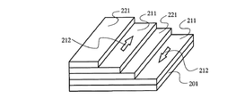
巨大磁気抵抗素子それぞれは、強磁性層と非磁性層とを交互に積層した積層薄膜であり、その長手方向寸法に対して薄膜の幅方向寸法が十分に小さい。例えば、Si基板上に85nm厚のAl2O3膜と5nm厚のNiFeCr膜とを下地膜として、その上に1.6nm厚のNiFeCoB合金からなる強磁性層と2.4nm厚のCu層(非磁性層)とを交互に14層ずつ積層した巨大磁気抵抗素子を用いることができる。図3に巨大磁気抵抗素子の一部を切り取って斜視図で示している。201は下地膜であり5nm厚のNiFeCr膜で、その上にNiFeCoBの強磁性層211とCuの非磁性層221とが積層されている。この図では強磁性層211を2層と非磁性層221を2層のみを示しているが、実際にはそれぞれ10〜15層ずつ積層されている。
Each giant magnetoresistive element is a laminated thin film in which ferromagnetic layers and nonmagnetic layers are alternately laminated, and the dimension in the width direction of the thin film is sufficiently smaller than the dimension in the longitudinal direction. For example, an 85 nm thick Al 2 O 3 film and a 5 nm thick NiFeCr film are used as a base film on a Si substrate, and a 1.6 nm thick NiFeCoB alloy ferromagnetic layer and a 2.4 nm thick Cu layer ( A giant magnetoresistive element in which 14 layers of nonmagnetic layers are alternately laminated can be used. FIG. 3 is a perspective view of a part of the giant magnetoresistive element cut out.
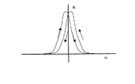
強磁性層211内の磁化は外部から磁界が印加されていない状態で矢印で示しているように、非磁性層221を挟んで隣り合っている強磁性層211の磁化212は反平行となっている。隣り合っている強磁性層211内の磁化212は互いに磁気結合しているので反平行となる。そのように隣り合っている強磁性層内の磁化が互いに反平行となっているときには、それら強磁性層に挟まれた非磁性層221を流れる電流に対する電気抵抗が最も大きい。外部磁界が加わって非磁性層221を挟む両側の強磁性層211の磁化が同じ方向に揃ってくると、電流に対する電気抵抗が小さくなる。外部磁界が加わらないときには、巨大磁気抵抗素子全体としては巨大磁気抵抗素子の面に平行ないずれの方向にも磁化がないすなわち結晶磁気異方性を持たず磁気的に等方性である。そのために巨大磁気抵抗素子面に平行ないずれかの方向に外部磁界が加わった場合、その磁界の大きさに応じて図4のカーブlのように抵抗が変わる。
The magnetization in the
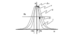
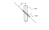
磁気的に等方性の材料であっても、その形状によって反磁界の大きさが異なるために形状異方性がある。本発明に用いている巨大磁気抵抗素子の様に長手方向寸法に対して薄膜の幅方向寸法が十分に小さいときには、巨大磁気抵抗素子薄膜の長手方向の反磁界は十分に小さく無視することができるが、その幅方向の反磁界が大きく、幅方向に外部磁界が印加されたときには巨大磁気抵抗素子内部の磁化に影響を及ぼす磁界は印加した磁界の強さから反磁界の強さを差し引いたものとなる。そこで、巨大磁気抵抗素子の幅方向に外部磁界を印加したときの巨大磁気抵抗素子の抵抗と外部磁界の大きさとの関係は図4のカーブvの様になる。他方、巨大磁気抵抗素子の長手方向に外部磁界を印加したときの巨大磁気抵抗素子の抵抗と外部磁界の大きさとの関係は同図のカーブlである。長手方向と横方向との中間すなわち図5で巨大磁気抵抗素子200の長手方向に対してある角度θで外部磁界300をかけたときの巨大磁気抵抗素子抵抗と外部磁界の大きさとの関係は図4でカーブlとカーブvとの間にあるカーブdの様になる。
Even a magnetically isotropic material has shape anisotropy because the magnitude of the demagnetizing field varies depending on its shape. When the dimension in the width direction of the thin film is sufficiently small with respect to the longitudinal dimension as in the giant magnetoresistive element used in the present invention, the demagnetizing field in the longitudinal direction of the giant magnetoresistive element thin film is sufficiently small and can be ignored. However, when the demagnetizing field in the width direction is large and an external magnetic field is applied in the width direction, the magnetic field that affects the magnetization inside the giant magnetoresistive element is obtained by subtracting the demagnetizing field strength from the applied magnetic field strength. It becomes. Therefore, the relationship between the resistance of the giant magnetoresistive element and the magnitude of the external magnetic field when an external magnetic field is applied in the width direction of the giant magnetoresistive element is as shown by a curve v in FIG. On the other hand, the relationship between the resistance of the giant magnetoresistive element and the magnitude of the external magnetic field when an external magnetic field is applied in the longitudinal direction of the giant magnetoresistive element is curve l in FIG. FIG. 5 shows the relationship between the giant magnetoresistive element resistance and the magnitude of the external magnetic field when the external
巨大磁気抵抗素子の磁化がその長手方向に少し揃って、図4のカーブlのほぼ中間程度の抵抗となる大きさの直流電流を平面コイルに流し、その直流電流をバイアス電流Ibとする。バイアス電流Ibによって各巨大磁気抵抗素子に加わる直流磁界をバイアス磁界Hbと呼ぶ。巨大磁気抵抗素子に更に外部磁界(例えば地磁気)Hexがx軸に対して角度θの方向に印加されると、外部磁界Hexのx方向成分Hx(=Hex・cosθ)によって、巨大磁気抵抗素子の抵抗は図4のカーブl上をバイアス点Rbから右下方向矢印の向きに変化する。その変化率を−βl(=ΔR/ΔH)とする。y方向磁界による抵抗変化は図4のカーブvなので、外部磁界Hexのy方向成分Hy(=Hex・sinθ)によって、巨大磁気抵抗素子の抵抗はカーブv上で右下方向矢印の向きに変化する。その変化率を−βv(=ΔR/ΔH)とする。y方向磁界による抵抗変化率βvはx方向磁界による抵抗変化率βlよりも小さく、幅方向寸法が長手方向に比して十分小さいすなわち細いときには抵抗変化率βvは極めて小さい値となる。 A direct current having a magnitude that causes the magnetization of the giant magnetoresistive element to be slightly aligned in the longitudinal direction and has a resistance approximately in the middle of the curve l in FIG. 4 is passed through the planar coil, and the direct current is defined as a bias current Ib. A DC magnetic field applied to each giant magnetoresistive element by the bias current Ib is called a bias magnetic field Hb. When an external magnetic field (for example, geomagnetism) Hex is further applied to the giant magnetoresistive element in the direction of the angle θ with respect to the x-axis, the x-direction component Hx (= Hex · cos θ) of the external magnetic field Hex causes The resistance changes on the curve l in FIG. 4 from the bias point Rb in the direction of the lower right arrow. The rate of change is -βl (= ΔR / ΔH). Since the resistance change due to the y-direction magnetic field is the curve v in FIG. 4, the resistance of the giant magnetoresistive element changes in the direction of the lower right arrow on the curve v due to the y-direction component Hy (= Hex · sin θ) of the external magnetic field Hex. . The rate of change is -βv (= ΔR / ΔH). The resistance change rate βv due to the y-direction magnetic field is smaller than the resistance change rate βl due to the x-direction magnetic field, and the resistance change rate βv is extremely small when the width direction dimension is sufficiently small, that is, thin.
平面コイル1にバイアス電流Ibを時計廻りに流しているときに、外部磁界Hexを実施例1の方位計にx軸と角度θを持って印加したとき巨大磁気抵抗素子21の抵抗R21は次式となる。
R21=Rb−βl・Hex・cosθ−βv・Hex・sinθ
巨大磁気抵抗素子22,31には外部磁界Hexと反対方向のバイアス磁界が印加されており、巨大磁気抵抗素子32には巨大磁気抵抗素子21に印加されているバイアス磁界と同じバイアス磁界が印加されているので、巨大磁気抵抗素子それぞれの抵抗R22,R31,R32は次のようになる。
R22=Rb+βl・Hex・cosθ−βv・Hex・sinθ
R31=Rb+βl・Hex・cosθ−βv・Hex・sinθ
R32=Rb−βl・Hex・cosθ−βv・Hex・sinθ
巨大磁気抵抗素子21と巨大磁気抵抗素子22の第一の中間電圧V2(正方向バイアス電流を流しているときの電圧を「第一」と呼ぶ)、巨大磁気抵抗素子31と巨大磁気抵抗素子32の第一の中間電圧V3それぞれは、
V2=Vcc・(Rb+βl・Hex・cosθ−βv・Hex・sinθ)/2(Rb−βv・Hex・sinθ)
V3=Vcc・(Rb−βl・Hex・cosθ−βv・Hex・sinθ)/2(Rb−βv・Hex・sinθ)
なので、これらの第一の中間電圧差Vx(+)(正方向バイアス電流を流している状態を「+」とする)は
Vx(+)=V2−V3=Vcc・βl・Hex・cosθ/(Rb−βv・Hex・sinθ)
となる。同様にして、巨大磁気抵抗素子対4と巨大磁気抵抗素子対5との第一の中間電圧差Vy(+)を求めると、
Vy(+)=V4−V5=Vcc・βl・Hex・sinθ/(Rb−βv・Hex・cosθ)
となる。
The resistance R21 of the
R21 = Rb−βl · Hex · cos θ−βv · Hex · sin θ
A bias magnetic field opposite to the external magnetic field Hex is applied to the giant
R22 = Rb + βl · Hex · cos θ−βv · Hex · sin θ
R31 = Rb + βl · Hex · cos θ−βv · Hex · sin θ
R32 = Rb-βl · Hex · cos θ-βv · Hex · sin θ
A first intermediate voltage V2 between the
V2 = Vcc · (Rb + βl · Hex · cos θ−βv · Hex · sin θ) / 2 (Rb−βv · Hex · sin θ)
V3 = Vcc · (Rb−βl · Hex · cos θ−βv · Hex · sin θ) / 2 (Rb−βv · Hex · sin θ)
Therefore, the first intermediate voltage difference Vx (+) (the state in which the positive direction bias current is flowing is “+”) is Vx (+) = V2−V3 = Vcc · βl · Hex · cos θ / ( Rb-βv · Hex · sinθ)
It becomes. Similarly, when the first intermediate voltage difference Vy (+) between the giant magnetoresistive element pair 4 and the giant magnetoresistive element pair 5 is obtained,
Vy (+) = V4−V5 = Vcc · βl · Hex · sinθ / (Rb−βv · Hex · cosθ)
It becomes.
次に平面コイル1にバイアス電流−Ibを反時計方向に流しているときに、外部磁界Hexによる第二の中間電圧差Vx(−)(負方向バイアス電流を流している状態を「−」として、「第二」と呼ぶ)と第二の中間電圧差Vy(−)は、それぞれ
Vx(−)=−Vcc・βl・Hex・cosθ/(Rb−βv・Hex・sinθ)
Vy(−)=−Vcc・βl・Hex・sinθ/(Rb−βv・Hex・cosθ)
となる。
Next, when the bias current −Ib is passed through the planar coil 1 in the counterclockwise direction, the second intermediate voltage difference Vx (−) due to the external magnetic field Hex (a state in which a negative bias current is passed is defined as “−”). The second intermediate voltage difference Vy (−) is expressed as Vx (−) = − Vcc · βl · Hex · cos θ / (Rb−βv · Hex · sin θ).
Vy (−) = − Vcc · βl · Hex · sinθ / (Rb−βv · Hex · cosθ)
It becomes.
平面コイル1に正方向バイアス電流を流しているときの第一の中間電圧差と負方向バイアス電流を流しているときの第二の中間電圧差との差をx方向の2組の巨大磁気抵抗素子対2,3について、またy方向の2組の巨大磁気抵抗素子対4,5について求めると、各々
Vx=Vx(+)−Vx(−)=2Vcc・βl・Hex・cosθ/(Rb−βv・Hex・sinθ)
Vy=Vy(+)−Vy(−)=2Vcc・βl・Hex・sinθ/(Rb−βv・Hex・cosθ)
となり、ここでβvはβlよりも極めて小さく、Rb>>βv・Hex・sinθ、Rb>>βv・Hex・cosθといえるので、
Vx≒2Vcc・βl・Hex・cosθ/Rb
Vy≒2Vcc・βl・Hex・sinθ/Rb
となる。
これらの式から、外部磁界の加わる角度θは、
θ=tan−1(Vy/Vx)
となるので、実施例1の方位計によって外部磁界の加わる角度θを求めることができる。
The difference between the first intermediate voltage difference when a positive bias current is passed through the planar coil 1 and the second intermediate voltage difference when a negative bias current is passed is the two giant magnetoresistives in the x direction. When the element pairs 2 and 3 and the two giant magnetoresistive element pairs 4 and 5 in the y direction are obtained, Vx = Vx (+) − Vx (−) = 2 Vcc · βl · Hex · cos θ / (Rb− βv ・ Hex ・ sinθ)
Vy = Vy (+) − Vy (−) = 2 Vcc · βl · Hex · sin θ / (Rb−βv · Hex · cos θ)
Here, βv is extremely smaller than βl, and it can be said that Rb >> βv · Hex · sinθ and Rb >> βv · Hex · cosθ.
Vx ≒ 2Vcc ・ βl ・ Hex ・ cosθ / Rb
Vy ≒ 2Vcc ・ βl ・ Hex ・ sinθ / Rb
It becomes.
From these equations, the angle θ applied by the external magnetic field is
θ = tan −1 (Vy / Vx)
Therefore, the angle θ applied by the external magnetic field can be obtained by the azimuth meter of the first embodiment.
上の説明では平面コイル1に流す電流は正方向バイアス電流Ibと負方向バイアス電流−Ibとについてのみ説明した。しかし、本発明で、平面コイルの好ましい電源としては、巨大磁気抵抗素子の磁化が長手方向に飽和する大きさの直流磁界を巨大磁気抵抗素子に印加するのに十分な直流電流を平面コイルに供給し、その直流磁界よりも小さな所定の直流磁界すなわちバイアス磁界を巨大磁気抵抗素子に印加するだけの直流電流を平面コイルに供給し、巨大磁気抵抗素子の磁化が前記と逆方向に飽和する大きさの直流磁界を巨大磁気抵抗素子に印加するのに十分な直流電流を平面コイルに供給し、そして上記所定の直流磁界と逆方向の所定の直流磁界すなわちバイアス磁界を印加するだけの直流電流を平面コイルに供給するものである。 In the above description, only the positive direction bias current Ib and the negative direction bias current −Ib have been described as the currents flowing through the planar coil 1. However, in the present invention, as a preferred power source for the planar coil, a sufficient DC current is supplied to the planar coil to apply a DC magnetic field with a magnitude that saturates the magnetization of the giant magnetoresistive element in the longitudinal direction. A DC current sufficient to apply a predetermined DC magnetic field, that is, a bias magnetic field, smaller than the DC magnetic field to the giant magnetoresistive element is supplied to the planar coil, and the magnetization of the giant magnetoresistive element is saturated in the opposite direction. A DC current sufficient to apply a DC magnetic field to the giant magnetoresistive element is supplied to the planar coil, and a DC current sufficient to apply a predetermined DC magnetic field, that is, a bias magnetic field opposite to the predetermined DC magnetic field is planar. It supplies to the coil.
巨大磁気抵抗素子に印加する外部磁界と巨大磁気抵抗素子の抵抗との関係には通常ヒステリシスがあり、磁界を負方向から増やしていく場合と正方向から減らしていく場合とは図6に示すように少し違ったループを取る。地磁気のように小さな磁界を測定する場合にはこの違いが無視できない。そこで本発明ではバイアス磁界を印加する前に予め飽和するだけの大きさの磁界をバイアス磁界と同じ方向にかけておき、磁界を減らしていって、バイアス磁界を印加することが望ましい。 There is usually hysteresis in the relationship between the external magnetic field applied to the giant magnetoresistive element and the resistance of the giant magnetoresistive element, and the case where the magnetic field is increased from the negative direction and the case where the magnetic field is decreased from the positive direction is as shown in FIG. Take a slightly different loop. This difference cannot be ignored when measuring small magnetic fields such as geomagnetism. Therefore, in the present invention, it is desirable to apply a bias magnetic field by applying a magnetic field having a magnitude sufficient to be saturated in advance in the same direction as the bias magnetic field before applying the bias magnetic field to reduce the magnetic field.
実施例2
本発明の方位計の実施例2について回路図を図7に示している。ここに示している方位計は図2の回路図に示した方位計から、巨大磁気抵抗素子対3と5を除いたものである。そのために、図2では巨大磁気抵抗素子対2と3の中間電圧差、及び巨大磁気抵抗素子対4と5の中間電圧差を求めていたのに対して、図7の方位計では巨大磁気抵抗素子対2と4それぞれの中間電圧を求めるようになっている。参照符号は図1、図2と同じものを用いて示している。
Example 2
FIG. 7 shows a circuit diagram of Example 2 of the compass of the present invention. The compass shown here is obtained by removing the giant magnetoresistive element pairs 3 and 5 from the compass shown in the circuit diagram of FIG. Therefore, in FIG. 2, the intermediate voltage difference between the giant magnetoresistive element pairs 2 and 3 and the intermediate voltage difference between the giant magnetoresistive element pairs 4 and 5 are obtained, whereas in the azimuth meter in FIG. The intermediate voltages of the element pairs 2 and 4 are obtained. Reference numerals are the same as those in FIGS. 1 and 2.
一方向に所定のバイアス磁界を印加したとき巨大磁気抵抗素子対2の第一の中間電圧を求めると、
Vx(+)=Vcc・(Rb+βl・Hex・cosθ−βv・Hex・sinθ)/2(Rb−βv・Hex・sinθ)
であり、反対方向に所定の直流磁界を印加したときの第二の中間電圧は
Vx(−)=Vcc・(Rb−βl・Hex・cosθ−βv・Hex・sinθ)/2(Rb−βv・Hex・sinθ)
である。
When a first intermediate voltage of the giant magnetoresistive element pair 2 is obtained when a predetermined bias magnetic field is applied in one direction,
Vx (+) = Vcc · (Rb + βl · Hex · cos θ−βv · Hex · sin θ) / 2 (Rb−βv · Hex · sin θ)
The second intermediate voltage when a predetermined DC magnetic field is applied in the opposite direction is Vx (−) = Vcc · (Rb−βl · Hex · cos θ−βv · Hex · sin θ) / 2 (Rb−βv · Hex · sinθ)
It is.
また、一方向に所定のバイアス磁界を印加したとき巨大磁気抵抗素子対4の第一の中間電圧を求めると、
Vy(+)=Vcc・(Rb+βl・Hex・sinθ−βv・Hex・cosθ)/2(Rb−βv・Hex・cosθ)
であり、反対方向に所定の直流磁界を印加したときの第二の中間電圧は
Vy(−)=Vcc・(Rb−βl・Hex・sinθ−βv・Hex・cosθ)/2(Rb−βv・Hex・cosθ)
なので、これら両中間電圧をx方向、y方向それぞれについて差を求めると、
x方向のVx=Vx(+)−Vx(−)
=Vcc・βl・Hex・cosθ/(Rb−βv・Hex・sinθ)
≒Vcc・βl・Hex・cosθ/Rb
y方向のVy=Vy(+)−Vy(−)
=Vcc・βl・Hex・sinθ/(Rb−βv・Hex・cosθ)
≒Vcc・βl・Hex・sinθ/Rb
となる。この出力を実施例1の出力と比べると、半分になっている。これは実施例1ではフルブリッジになっていたものが、ここではハーフブリッジになっているためである。外部磁界の水平成分がx軸となす角度θは
θ=tan−1(Vy/Vx)
として求めることができる。
Further, when the first intermediate voltage of the giant magnetoresistive element pair 4 is obtained when a predetermined bias magnetic field is applied in one direction,
Vy (+) = Vcc · (Rb + βl · Hex · sin θ−βv · Hex · cos θ) / 2 (Rb−βv · Hex · cos θ)
The second intermediate voltage when a predetermined DC magnetic field is applied in the opposite direction is Vy (−) = Vcc · (Rb−βl · Hex · sin θ−βv · Hex · cos θ) / 2 (Rb−βv · Hex / cos θ)
So, when the difference between these two intermediate voltages in the x direction and the y direction is obtained,
x direction Vx = Vx (+) − Vx (−)
= Vcc · βl · Hex · cosθ / (Rb-βv · Hex · sinθ)
≒ Vcc ・ βl ・ Hex ・ cosθ / Rb
Vy in the y direction = Vy (+) − Vy (−)
= Vcc · βl · Hex · sinθ / (Rb-βv · Hex · cosθ)
≒ Vcc ・ βl ・ Hex ・ sinθ / Rb
It becomes. Compared with the output of Example 1, this output is halved. This is because the full bridge in the first embodiment is a half bridge here. The angle θ between the horizontal component of the external magnetic field and the x axis is θ = tan −1 (Vy / Vx).
Can be obtained as
この実施例において上の説明から明らかなように、一方向に直流電流を流しているときに巨大磁気抵抗素子対2および巨大磁気抵抗素子対4にx方向とy方向のバイアスを印加したときの中間電位出力を同時に求めることができる。とともに、反対方向に直流電流を流しているときに巨大磁気抵抗素子対2および巨大磁気抵抗素子対4に−x方向と−y方向のバイアスを印加したときの中間電位出力も同時に求めることができる
実施例3
本発明の方位計の実施例3について、回路図を図8に示している。ここに示している方位計は図7の回路図に示した方位計から、更に巨大磁気抵抗素子対4を除いたものである。ここでは巨大磁気抵抗素子対2の中間電圧を求めるようになっている。参照符号は図1、2、7と同じものを用いて示している。
As is apparent from the above description in this embodiment, when a bias in the x direction and the y direction is applied to the giant magnetoresistive element pair 2 and the giant magnetoresistive element pair 4 when a direct current flows in one direction. The intermediate potential output can be obtained simultaneously. At the same time, an intermediate potential output when biases in the −x direction and the −y direction are applied to the giant magnetoresistive element pair 2 and the giant magnetoresistive element pair 4 when a direct current is passed in the opposite direction can be obtained simultaneously. Example 3
A circuit diagram of Example 3 of the compass of the present invention is shown in FIG. The compass shown here is obtained by removing the giant magnetoresistive element pair 4 from the compass shown in the circuit diagram of FIG. Here, the intermediate voltage of the giant magnetoresistive element pair 2 is obtained. The reference numerals are the same as those shown in FIGS.
一方向に電流を流して、所定の磁界を印加したときの巨大磁気抵抗素子対2の第一の中間電圧は実施例1,2と同様に
Vx(+)=Vcc・(Rb+βl・Hex・cosθ−βv・Hex・sinθ)/2(Rb−βv・Hex・sinθ)
であり、反対方向に電流を流して、所定の磁界を印加したときの巨大磁気抵抗素子対2の第二の中間電圧は同様にして
Vx(−)=Vcc・(Rb−βl・Hex・cosθ−βv・Hex・sinθ)/2(Rb−βv・Hex・sinθ)
となる。これら両方向磁界を印加したときの両中間電圧の間の差を求めると
x方向のVx=Vx(+)−Vx(−)≒Vcc・βlHex・cosθ/Rb
となる。この式から地磁気の水平成分のx軸との角度θを求めることができる。しかし、y方向の出力差Vを測定していないので+/−θの区別が出来ないという欠点がある。
The first intermediate voltage of the giant magnetoresistive element pair 2 when a current is applied in one direction and a predetermined magnetic field is applied is Vx (+) = Vcc · (Rb + βl · Hex · cos θ as in the first and second embodiments. -Βv · Hex · sinθ) / 2 (Rb-βv · Hex · sinθ)
The second intermediate voltage of the giant magnetoresistive element pair 2 when a predetermined magnetic field is applied by passing a current in the opposite direction is similarly Vx (−) = Vcc · (Rb−βl · Hex · cos θ -Βv · Hex · sinθ) / 2 (Rb-βv · Hex · sinθ)
It becomes. When the difference between the two intermediate voltages when these bidirectional magnetic fields are applied is determined, Vx in the x direction = Vx (+) − Vx (−) ≈Vcc · βlHex · cos θ / Rb
It becomes. From this equation, the angle θ of the horizontal component of geomagnetism with the x-axis can be obtained. However, since the output difference V in the y direction is not measured, there is a drawback that +/− θ cannot be distinguished.
本発明の実施例1〜3から明らかなように、本発明の方位計はいずれも外部からかけた磁界の方向を測定することができる。この方位計は等方性巨大磁気抵抗素子を用いて、その形状異方性を使って方位を測定している。結晶磁気異方性を持たない巨大磁気抵抗素子を用いているので、巨大磁気抵抗素子を形成する際に磁界をかける必要がなく、実施例1のように巨大磁気抵抗素子を8個使っている場合でも、同じプロセス内で同時にそれら巨大磁気抵抗素子を作ることができる。巨大磁気抵抗素子の長手方向寸法に比して幅寸法を極めて小さくすることができる。そのために、巨大磁気抵抗素子の抵抗を大きくすることができ、測定時の発熱を小さくすることができる。更に、巨大磁気抵抗素子の長手方向磁界に対しては感度が良く、それに垂直な磁界に対しては感度が低いので、測定する方向の磁界に対して感度を上げることができる。 As is apparent from Examples 1 to 3 of the present invention, any of the compass of the present invention can measure the direction of a magnetic field applied from the outside. This compass uses an isotropic giant magnetoresistive element and measures its orientation using its shape anisotropy. Since a giant magnetoresistive element having no magnetocrystalline anisotropy is used, it is not necessary to apply a magnetic field when forming the giant magnetoresistive element, and eight giant magnetoresistive elements are used as in the first embodiment. Even in the same process, these giant magnetoresistive elements can be made simultaneously in the same process. The width dimension can be made extremely smaller than the longitudinal dimension of the giant magnetoresistive element. Therefore, the resistance of the giant magnetoresistive element can be increased, and the heat generation during measurement can be reduced. Furthermore, the sensitivity to the longitudinal magnetic field of the giant magnetoresistive element is good and the sensitivity to the magnetic field perpendicular to the longitudinal magnetic field is low. Therefore, the sensitivity can be increased with respect to the magnetic field in the measuring direction.
1 平面コイル
11,12,13,14 (平面コイルの)辺
2,3,4,5 巨大磁気抵抗素子対
21,22,31,32,41,42,51,52,200 巨大磁気抵抗素子
201 下地層
211 強磁性層
212 磁化
221 非磁性層
300 外部磁界
6,7,8,9 磁気抵抗素子対
61,62,71,72,81,82,91,92 磁気抵抗素子
DESCRIPTION OF SYMBOLS 1
Claims (5)
その平面コイル面の同じ側にあって、平面コイル面に平行で近接した平面内に設けられた巨大磁気抵抗素子2個からなる少なくとも1組の巨大磁気抵抗素子対とを有しており、
前記巨大磁気抵抗素子それぞれは、強磁性層と非磁性層とを交互に積層した積層薄膜であり、その長手方向寸法に対して薄膜の幅方向寸法が十分に小さな形状をしており、
前記巨大磁気抵抗素子対の各巨大磁気抵抗素子の長手方向は前記平面コイルの対辺対の各1辺のみと実質的に直交しており、
巨大磁気抵抗素子対の巨大磁気抵抗素子の一方の端部同士が接続されているとともに、他方の端部間に測定用電圧が印加されるようになっており、前記一方の端部から中間電圧を取り出すようになっていることを特徴とする方位計。 A planar coil at least partially having opposite sides parallel to each other;
Having at least one giant magnetoresistive element pair consisting of two giant magnetoresistive elements provided in a plane parallel to and close to the planar coil surface on the same side of the planar coil surface;
Each of the giant magnetoresistive elements is a laminated thin film in which ferromagnetic layers and nonmagnetic layers are alternately laminated, and the width direction dimension of the thin film is sufficiently small with respect to its longitudinal dimension.
The longitudinal direction of each giant magnetoresistive element of the giant magnetoresistive element pair is substantially orthogonal to only one side of the opposite side pair of the planar coil,
One end of the giant magnetoresistive element of the giant magnetoresistive element pair is connected to each other, and a measurement voltage is applied between the other end, and an intermediate voltage is applied from the one end. An azimuth meter characterized by taking out
前記巨大磁気抵抗素子に前記直流磁界よりも小さな所定の直流磁界を印加する直流電流を前記平面コイルに供給し、
前記巨大磁気抵抗素子の磁化が前記と逆方向に飽和する大きさの直流磁界を前記巨大磁気抵抗素子に印加するのに十分な直流電流を前記平面コイルに供給し、そして
前記巨大磁気抵抗素子に前記所定の直流磁界と逆方向の所定の直流磁界を印加する直流電流を前記平面コイルに供給する電源を更に有している請求項1から3のいずれか記載の方位計。 Supplying a DC current sufficient to apply to the giant magnetoresistive element a direct current magnetic field having a magnitude such that the magnetization of the giant magnetoresistive element saturates in the longitudinal direction;
A DC current that applies a predetermined DC magnetic field smaller than the DC magnetic field to the giant magnetoresistive element is supplied to the planar coil;
Sufficient DC current is applied to the planar coil to apply a DC magnetic field with a magnitude that causes the magnetization of the giant magnetoresistive element to saturate in the opposite direction to the giant magnetoresistive element, and to the giant magnetoresistive element The azimuth meter according to any one of claims 1 to 3, further comprising a power source that supplies a DC current that applies a predetermined DC magnetic field in a direction opposite to the predetermined DC magnetic field to the planar coil.
前記巨大磁気抵抗素子に前記逆方向の所定の直流磁界を印加している間に各巨大磁気抵抗素子対の前記一方の端部から第二の中間電圧を取り出し、
第一と第二の中間電圧の差に基づいて外部磁界の方位を求める演算器を更に有している請求項4記載の方位計。 Taking out a first intermediate voltage from the one end of each giant magnetoresistive element pair while applying the predetermined DC magnetic field to the giant magnetoresistive element;
Taking out a second intermediate voltage from the one end of each giant magnetoresistive element pair while applying the predetermined DC magnetic field in the reverse direction to the giant magnetoresistive element;
5. An azimuth meter according to claim 4, further comprising an arithmetic unit for obtaining the direction of the external magnetic field based on the difference between the first and second intermediate voltages.
Priority Applications (1)
| Application Number | Priority Date | Filing Date | Title |
|---|---|---|---|
| JP2004102764A JP4482866B2 (en) | 2004-03-31 | 2004-03-31 | A compass with a giant magnetoresistive element |
Applications Claiming Priority (1)
| Application Number | Priority Date | Filing Date | Title |
|---|---|---|---|
| JP2004102764A JP4482866B2 (en) | 2004-03-31 | 2004-03-31 | A compass with a giant magnetoresistive element |
Publications (3)
| Publication Number | Publication Date |
|---|---|
| JP2005291728A true JP2005291728A (en) | 2005-10-20 |
| JP2005291728A5 JP2005291728A5 (en) | 2006-08-31 |
| JP4482866B2 JP4482866B2 (en) | 2010-06-16 |
Family
ID=35324841
Family Applications (1)
| Application Number | Title | Priority Date | Filing Date |
|---|---|---|---|
| JP2004102764A Expired - Fee Related JP4482866B2 (en) | 2004-03-31 | 2004-03-31 | A compass with a giant magnetoresistive element |
Country Status (1)
| Country | Link |
|---|---|
| JP (1) | JP4482866B2 (en) |
Cited By (10)
| Publication number | Priority date | Publication date | Assignee | Title |
|---|---|---|---|---|
| JP2008096131A (en) * | 2006-10-06 | 2008-04-24 | Ricoh Co Ltd | Sensor module, correction method, program, and recording medium |
| JP2009236889A (en) * | 2008-03-28 | 2009-10-15 | Tdk Corp | Magnetic field measurement method and magnetic sensor |
| JP2009250931A (en) * | 2008-04-10 | 2009-10-29 | Rohm Co Ltd | Magnetic sensor, operation method thereof, and magnetic sensor system |
| JP2011047929A (en) * | 2009-07-29 | 2011-03-10 | Tdk Corp | Magnetic sensor |
| JP2012017990A (en) * | 2010-07-06 | 2012-01-26 | Denso Corp | Magnetic sensor device |
| JP2014006127A (en) * | 2012-06-22 | 2014-01-16 | Asahi Kasei Electronics Co Ltd | Multiaxial magnetic sensor and method of manufacturing the same |
| WO2015125699A1 (en) * | 2014-02-19 | 2015-08-27 | アルプス電気株式会社 | Magnetic sensor |
| CN109061528A (en) * | 2018-08-02 | 2018-12-21 | 华中科技大学 | A kind of three axial plane Magnetic Sensors based on giant magnetoresistance effect |
| JP2020511663A (en) * | 2017-03-24 | 2020-04-16 | 江▲蘇▼多▲維▼科技有限公司Multidimension Technology Co., Ltd. | Magnetic sensor packaging structure with hysteresis coil |
| CN113981334A (en) * | 2021-11-02 | 2022-01-28 | 浙江大学 | Amorphous wire planar structure with ultrahigh magnetic impedance and sensing application thereof |
-
2004
- 2004-03-31 JP JP2004102764A patent/JP4482866B2/en not_active Expired - Fee Related
Cited By (13)
| Publication number | Priority date | Publication date | Assignee | Title |
|---|---|---|---|---|
| JP2008096131A (en) * | 2006-10-06 | 2008-04-24 | Ricoh Co Ltd | Sensor module, correction method, program, and recording medium |
| JP2009236889A (en) * | 2008-03-28 | 2009-10-15 | Tdk Corp | Magnetic field measurement method and magnetic sensor |
| JP2009250931A (en) * | 2008-04-10 | 2009-10-29 | Rohm Co Ltd | Magnetic sensor, operation method thereof, and magnetic sensor system |
| JP2011047929A (en) * | 2009-07-29 | 2011-03-10 | Tdk Corp | Magnetic sensor |
| JP2012017990A (en) * | 2010-07-06 | 2012-01-26 | Denso Corp | Magnetic sensor device |
| JP2014006127A (en) * | 2012-06-22 | 2014-01-16 | Asahi Kasei Electronics Co Ltd | Multiaxial magnetic sensor and method of manufacturing the same |
| WO2015125699A1 (en) * | 2014-02-19 | 2015-08-27 | アルプス電気株式会社 | Magnetic sensor |
| JP2020511663A (en) * | 2017-03-24 | 2020-04-16 | 江▲蘇▼多▲維▼科技有限公司Multidimension Technology Co., Ltd. | Magnetic sensor packaging structure with hysteresis coil |
| JP7072265B2 (en) | 2017-03-24 | 2022-05-20 | 江▲蘇▼多▲維▼科技有限公司 | Magnetic sensor packaging structure with hysteresis coil |
| CN109061528A (en) * | 2018-08-02 | 2018-12-21 | 华中科技大学 | A kind of three axial plane Magnetic Sensors based on giant magnetoresistance effect |
| CN109061528B (en) * | 2018-08-02 | 2020-08-18 | 华中科技大学 | Three-axis planar magnetic sensor based on giant magneto-impedance effect |
| CN113981334A (en) * | 2021-11-02 | 2022-01-28 | 浙江大学 | Amorphous wire planar structure with ultrahigh magnetic impedance and sensing application thereof |
| CN113981334B (en) * | 2021-11-02 | 2022-04-26 | 浙江大学 | Amorphous filament planar structure with ultra-high magnetic impedance and its sensing applications |
Also Published As
| Publication number | Publication date |
|---|---|
| JP4482866B2 (en) | 2010-06-16 |
Similar Documents
| Publication | Publication Date | Title |
|---|---|---|
| US9069033B2 (en) | 3-axis magnetic field sensor, method for fabricating magnetic field sensing structure and magnetic field sensing circuit | |
| US7737678B2 (en) | Magnetic sensor and current sensor | |
| JP5152495B2 (en) | Magnetic sensor and portable information terminal device | |
| CN1924603B (en) | Magnetic field detection apparatus and method of adjusting the same | |
| CN102435960B (en) | Tunneling magnetoresistive structure and integrated 3-axis magnetic field sensor and manufacturing method thereof | |
| JP3573100B2 (en) | Compass and direction measurement method | |
| WO2020250489A1 (en) | Magnetic sensor, magnetic sensor array, magnetic field distribution measurement device, and position identification device | |
| JP2014516406A (en) | Single chip bridge type magnetic field sensor and manufacturing method thereof | |
| JP2007101253A (en) | Current sensor | |
| WO2005081007A1 (en) | Magnetic field detector, current detector, position detector and rotation detector employing it | |
| JP2016176911A (en) | Magnetic sensor | |
| JPWO2020208907A1 (en) | Magneto Resistive Sensor and Magnetometer | |
| CN106597326A (en) | Magnetic field sensing device | |
| JP4023476B2 (en) | A compass with a spin-valve giant magnetoresistive element | |
| JP4508058B2 (en) | Magnetic field detection device and manufacturing method thereof | |
| JP4482866B2 (en) | A compass with a giant magnetoresistive element | |
| US9372242B2 (en) | Magnetometer with angled set/reset coil | |
| US12498434B2 (en) | Magnetic sensor element, magnetic sensor, and magnetic sensor device | |
| TW201715251A (en) | Magnetic field sensing apparatus | |
| JP2003533895A (en) | Magnetic field sensor using magnetoresistance and manufacturing method thereof | |
| JP2014089088A (en) | Magnetoresistive effect element | |
| JP2012063203A (en) | Magnetic sensor | |
| CN109541503A (en) | Magnetic Sensor | |
| JP2003215222A (en) | Magneto-resistance effect element sensor | |
| JP2012063232A (en) | Method for manufacturing magnetic field detection apparatus, and magnetic field detection apparatus |
Legal Events
| Date | Code | Title | Description |
|---|---|---|---|
| A521 | Written amendment |
Free format text: JAPANESE INTERMEDIATE CODE: A523 Effective date: 20060713 |
|
| A621 | Written request for application examination |
Free format text: JAPANESE INTERMEDIATE CODE: A621 Effective date: 20060713 |
|
| A131 | Notification of reasons for refusal |
Free format text: JAPANESE INTERMEDIATE CODE: A131 Effective date: 20090721 |
|
| A521 | Written amendment |
Free format text: JAPANESE INTERMEDIATE CODE: A523 Effective date: 20090914 |
|
| RD04 | Notification of resignation of power of attorney |
Free format text: JAPANESE INTERMEDIATE CODE: A7424 Effective date: 20100202 |
|
| TRDD | Decision of grant or rejection written | ||
| A01 | Written decision to grant a patent or to grant a registration (utility model) |
Free format text: JAPANESE INTERMEDIATE CODE: A01 Effective date: 20100226 |
|
| A01 | Written decision to grant a patent or to grant a registration (utility model) |
Free format text: JAPANESE INTERMEDIATE CODE: A01 |
|
| A61 | First payment of annual fees (during grant procedure) |
Free format text: JAPANESE INTERMEDIATE CODE: A61 Effective date: 20100311 |
|
| R150 | Certificate of patent or registration of utility model |
Free format text: JAPANESE INTERMEDIATE CODE: R150 |
|
| FPAY | Renewal fee payment (event date is renewal date of database) |
Free format text: PAYMENT UNTIL: 20130402 Year of fee payment: 3 |
|
| FPAY | Renewal fee payment (event date is renewal date of database) |
Free format text: PAYMENT UNTIL: 20130402 Year of fee payment: 3 |
|
| FPAY | Renewal fee payment (event date is renewal date of database) |
Free format text: PAYMENT UNTIL: 20140402 Year of fee payment: 4 |
|
| LAPS | Cancellation because of no payment of annual fees |