JP2005291722A - Probe unit and method of manufacturing probe unit - Google Patents
Probe unit and method of manufacturing probe unit Download PDFInfo
- Publication number
- JP2005291722A JP2005291722A JP2004102619A JP2004102619A JP2005291722A JP 2005291722 A JP2005291722 A JP 2005291722A JP 2004102619 A JP2004102619 A JP 2004102619A JP 2004102619 A JP2004102619 A JP 2004102619A JP 2005291722 A JP2005291722 A JP 2005291722A
- Authority
- JP
- Japan
- Prior art keywords
- wiring film
- probe unit
- probe
- bump
- substrate
- Prior art date
- Legal status (The legal status is an assumption and is not a legal conclusion. Google has not performed a legal analysis and makes no representation as to the accuracy of the status listed.)
- Withdrawn
Links
Images
Landscapes
- Testing Of Individual Semiconductor Devices (AREA)
- Measuring Leads Or Probes (AREA)
Abstract
Description
本発明は、半導体集積回路や液晶パネル等の電子デバイスの電気的特性を検査するためのプローブユニット及びプローブユニットの製造方法に関する。 The present invention relates to a probe unit for inspecting electrical characteristics of an electronic device such as a semiconductor integrated circuit and a liquid crystal panel, and a method of manufacturing the probe unit.
従来、フォトリソグラフィを用いて形成された薄膜状のプローブが基板上に狭小なピッチで多数並び、各プローブの先端が基板の縁から櫛歯状に突出したプローブユニットが知られている。このようなプローブユニットは、電子デバイスの電極ピッチの狭小化に対応して開発されたものである。このようなプローブユニットは、そのプローブ(以下、櫛歯状薄膜プローブという。)の先端が直線的に整列しているため、各電極の表面が平坦な電子デバイスの検査に好適である。検査時は、櫛歯状薄膜プローブを検体の各電極に一本づつ接触させる。 2. Description of the Related Art Conventionally, a probe unit is known in which a large number of thin-film probes formed by photolithography are arranged on a substrate at a narrow pitch, and the tips of the probes protrude from the edge of the substrate in a comb shape. Such a probe unit has been developed in response to the narrowing of the electrode pitch of an electronic device. Such a probe unit is suitable for inspection of an electronic device having a flat surface of each electrode because the tips of the probes (hereinafter referred to as comb-shaped thin film probes) are linearly aligned. At the time of inspection, a comb-like thin film probe is brought into contact with each electrode of the specimen one by one.
ところで近年、WL−CSP(Wafer Level - Chip Size Package)の製品化が活発である。WL−CSP等の小型電子デバイスの電極には、半田などが台地状又はこぶ状に盛り上がったバンプになっているものがある。しかし、バンプの表面が盛り上がっており、その隆起形状も均一でないため、パッケージの表面に配列された複数のバンプに、櫛歯状薄膜プローブの直線的に整列した先端部を同時に確実に接触させることは困難である。 Incidentally, in recent years, WL-CSP (Wafer Level-Chip Size Package) has been actively commercialized. Some electrodes of small electronic devices such as WL-CSP are bumps in which solder or the like is raised in a plateau or hump shape. However, since the bump surface is raised and the raised shape is not uniform, the linearly aligned tips of the comb-like thin film probe are simultaneously and reliably brought into contact with a plurality of bumps arranged on the surface of the package. It is difficult.
複数のバンプと確実な接触が得られるプローブとしては、王冠のように複数の突部が環状に連なった形状の先端部を持つ棒状のプローブが知られている。このようなプローブは、基板と別体に成形された後、基板に固定される。したがって、このようなプローブをバンプのピッチに応じて狭小なピッチで基板上に配列することは困難である。 As a probe capable of obtaining reliable contact with a plurality of bumps, a rod-like probe having a tip portion in which a plurality of protrusions are connected in a ring like a crown is known. Such a probe is formed separately from the substrate and then fixed to the substrate. Therefore, it is difficult to arrange such probes on the substrate at a narrow pitch according to the pitch of the bumps.
特許文献1、2には、バンプが狭小なピッチで配列されたWL−CSPの検査に好適な多点接続シートとその製造方法が開示されている。
しかし、特許文献1、2に開示された多点接続シートは、複雑な製造プロセスを必要とする円筒状のプローブを備えたものである。また、円筒状のプローブの端部内側に球状のバンプを接触させると、バンプとプローブが環状に接触するため、バンプとプローブの接触圧が点接触の場合に比べて低くなるという問題がある。
However, the multipoint connection sheet disclosed in
本発明は、これらの問題を解決するために創作されたものであって、バンプが狭小なピッチで複数配列された電子デバイスの電気的特性を確実に検査できるプローブユニットを提供することを目的とする。
また本発明は、バンプが狭小なピッチで複数配列された電子デバイスの電気的特性を確実に検査できるプローブユニットの簡素な製造方法を提供することを目的とする。
The present invention was created to solve these problems, and an object thereof is to provide a probe unit capable of reliably inspecting the electrical characteristics of an electronic device in which a plurality of bumps are arranged at a narrow pitch. To do.
It is another object of the present invention to provide a simple manufacturing method of a probe unit that can reliably inspect the electrical characteristics of an electronic device in which a plurality of bumps are arranged at a narrow pitch.
上記第一の目的を達成するため、本発明に係るプローブユニットは、基板と、輪郭が蛇行した複数の開口を有し、前記基板の表面上に形成された配線膜とを備え、前記配線膜の各開口の複数の凸縁は、前記基板の表面から隆起し、検体のバンプに接触する接触部を形成していることを特徴とする。基板の表面上に形成された配線膜で接触部を形成することにより、基板上に狭小なピッチで複数の接触部を配列することができる。配線膜の凸縁を隆起させて接触部を形成することにより、接触部と検体のバンプとを点接触させることができる。また、配線膜に形成する開口の輪郭を蛇行させることにより、各開口について配線膜に複数の凸縁を形成すると、各バンプに複数の凸縁を対応させることができる。各バンプに複数の凸縁を対応させることにより、複数のバンプを同時に確実に配線膜と電気的に接続することができる。したがって、本発明に係るプローブユニットによると、バンプが狭小なピッチで複数配列された電子デバイスの電気的特性を確実に検査できる。 In order to achieve the first object, a probe unit according to the present invention includes a substrate, and a wiring film having a plurality of openings with meandering contours and formed on the surface of the substrate, and the wiring film The plurality of convex edges of each of the openings are raised from the surface of the substrate to form a contact portion that contacts a bump of the specimen. By forming the contact portion with a wiring film formed on the surface of the substrate, a plurality of contact portions can be arranged on the substrate with a narrow pitch. By forming the contact portion by raising the convex edge of the wiring film, the contact portion and the bump of the specimen can be brought into point contact. In addition, when the plurality of convex edges are formed in the wiring film for each opening by meandering the outline of the opening formed in the wiring film, the plurality of convex edges can correspond to each bump. By making a plurality of convex edges correspond to each bump, the plurality of bumps can be electrically connected to the wiring film reliably at the same time. Therefore, according to the probe unit of the present invention, the electrical characteristics of an electronic device in which a plurality of bumps are arranged at a narrow pitch can be reliably inspected.
上記第二の目的を達成するため、本発明に係るプローブユニットの製造方法は、輪郭が蛇行した複数の開口を有する配線膜を基板の表面上に形成する工程と、前記基板の各開口の近傍を除去して通孔を形成する工程と、前記通孔から前記配線膜の各開口の複数の凸縁を突き上げ、前記凸縁を検体のバンプに接触する接触部に成形する工程と、を含むことを特徴とする。基板の表面上に形成する配線膜に輪郭が蛇行した複数の開口を形成する工程は簡素である。基板の各開口の近傍を除去して通孔を形成する工程も簡素である。通孔から配線膜の各開口の複数の凸縁を突き上げる工程も簡素である。したがって、本発明に係る製造方法によると、バンプが狭小なピッチで複数配列された電子デバイスの電気的特性を確実に検査できるプローブユニットを簡素な工程で製造できる。 In order to achieve the second object, a method for manufacturing a probe unit according to the present invention includes a step of forming a wiring film having a plurality of openings having meandering contours on a surface of a substrate, and the vicinity of each opening of the substrate. And forming a through hole, and pushing up a plurality of convex edges of each opening of the wiring film from the through hole, and forming the convex edges into contact portions that contact the bumps of the specimen. It is characterized by that. The process of forming a plurality of openings whose contours meander in the wiring film formed on the surface of the substrate is simple. The process of removing the vicinity of each opening of the substrate and forming the through hole is also simple. The process of pushing up the plurality of convex edges of each opening of the wiring film from the through hole is also simple. Therefore, according to the manufacturing method according to the present invention, a probe unit capable of reliably inspecting the electrical characteristics of an electronic device in which a plurality of bumps are arranged at a narrow pitch can be manufactured in a simple process.
以下、本発明の実施例を図面に基づいて説明する。
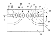
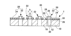
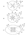
まず本発明の一実施例によるプローブユニットについて説明する。図1はプローブユニット1を示す平面図である。図2は図1のA−A線断面図である。
プローブユニット1は、図1及び図2に示すように、プローブ22及びリード24に区分される配線膜20が基板10上に接着剤30によって貼り付けられている。配線膜20には例えばNi、Ni−W、NiFeなどのニッケル合金などの金属などが用いられる。プローブ22は基板10上に複数配列され、それらプローブ22からそれぞれリード24が延伸するように設けられている。各プローブ22は、輪郭が蛇行し略十字形をなす開口26を中心に有し、開口26の四つの凸縁28が基板10表面から隆起しているため、王冠のように構成されている。開口26の四つの凸縁28は検体のバンプと接触する接触部を形成している。開口26の大きさは、例えば上端の最小幅aが約0.2mmであり、下端の直径bが約0.6mmである。凸縁28のリード24表面を基準とした高さは例えば約0.5mmである。基板10は、開口26下部に円柱形の通孔12を有する。
Embodiments of the present invention will be described below with reference to the drawings.
First, a probe unit according to an embodiment of the present invention will be described. FIG. 1 is a plan view showing the
As shown in FIGS. 1 and 2, the
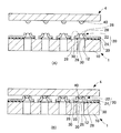
次に、プローブユニット1を用いた導通試験方法について説明する。図3は、導通試験方法を示す断面図である。
はじめに図3(A)に示すように、各プローブ22が検体4の各バンプ40に対向するようにプローブユニット1を配置する。その後、図3(B)に示すように検体4にプローブユニット1を押し当て、プローブ22の開口26の各凸縁28で各バンプ40を挟み付けるようにして凸縁28とバンプ40とを接触させ、配線膜20とバンプ40との間で導通試験を行う。このとき凸縁28は、バンプ40の曲面形状に合わせて撓んでバンプ40をしっかりと挟み込み、確実にバンプ40と接触することができる。
Next, a continuity test method using the
First, as shown in FIG. 3A, the
本実施例によると、配線膜20を基板10の表面上に従来の薄膜製造技術を用いて形成することができるため、配線膜20で形成される複数のプローブ22を基板10上に狭小なピッチで配列することができる。また、プローブ22の開口26の輪郭を蛇行させ、隆起した四つの凸縁28で一つのバンプ40に対応する接触部を形成することにより、接触部とバンプ40とを四点接触させることができる。バンプ40と四点接触する接触部をもつプローブ22を基板10上に複数配列することにより、複数のバンプ40を接触圧を低下させることなく同時に確実に配線膜20と接続できる。したがって、本実施例のプローブユニット1によれば、狭小なピッチで配列された複数のバンプをもつ電子デバイスの電気的特性を確実に検査可能である。さらに本実施例のプローブユニット1を電子デバイスのバーンインに用いることも可能である。
According to the present embodiment, since the
なお、凸縁28の数は四つに限らず、接触部とバンプ40との電気的接続をより確実にするために、開口26の形状を変えて凸縁28の数を多くしてもよい。導通検査時において凸縁28でバンプ40をしっかりと挟み付けるために、凸縁28は三つ以上が好ましい。
またプローブ22とリード24は、同じ材質でなくともよい。導通検査時にバンプ40との接触によりプローブ22に負荷がかかることを考慮して、プローブ22が優れた耐久性を有するように、プローブ22をリード24より硬い材質にしてもよい。
The number of the
Further, the
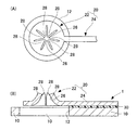
次に、プローブユニット1の製造方法について説明する。
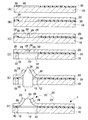
図4は、プローブユニット1の製造方法を示す断面図である。
はじめに図4(A)に示すように、基板10の一方の表面に、プローブを形成する部分を除いて接着剤30を塗布する。
次に図4(B)に示すように、接着剤30によって基板10に配線膜20を貼り付ける。配線膜20には例えばNi、Ni−W、NiFeなどのニッケル合金、または金属ガラスなどを用いる。
Next, a method for manufacturing the
FIG. 4 is a cross-sectional view showing a method for manufacturing the
First, as shown in FIG. 4A, an adhesive 30 is applied to one surface of the
Next, as shown in FIG. 4B, the
次に図4(C)に示すように、リソグラフィー及びエッチングにより配線膜20をパターニングし、プローブ22の外郭とリード24とを形成すると同時にプローブ22の中心に開口26を形成する。この開口26の形成は、スタンピングによっても行うことができる。開口26をスタンピングによって形成した場合、配線膜20のプローブ22の外郭とリード24のパターニングは別工程で行わなければならない。
Next, as shown in FIG. 4C, the
次に図4(D)に示すように、基板10の開口26周辺をドリル加工などにより除去し、基板10に通孔12を形成する。
次に図4(E)に示すように、先端が尖った硬い金属棒5などで配線膜20の凸縁28を通孔12から突き上げて隆起させる。
最後に、配線膜20のエッチングによって表面に露出した不要な接着剤30を除去すると、図4(F)に示すようにプローブユニット1が完成する。
Next, as shown in FIG. 4D, the periphery of the
Next, as shown in FIG. 4E, the
Finally, when the
図5は、図4(C)に示した開口形成工程でパターニングされた配線膜20を示す平面図である。
図5(A)に示すように、四つの凸縁28が形成される開口26を形成すると、この凸縁28を突き上げて隆起させれば、四つの凸縁28が環状に連なった上述のプローブユニット1を形成することができる。図5(B)に示すように、七つの凸縁28が形成される開口26を形成すると、七つの凸縁28が環状に連なった上述のプローブユニット1を形成することができる。図5(C)に示すように、開口26自体を蛇腹状に形成して五つの凸縁28を形成し、プローブ22の外縁を略楕円形に形成してもよい。このように凸縁28の根元からの長さを長く形成すれば、凸縁28を高く隆起させることができる。また、通孔を大きくすることによって、図6のようにプローブ22の凸縁28を長くし、ばね性をもたせることができる。
FIG. 5 is a plan view showing the
As shown in FIG. 5A, when the
本製造方法によれば、バンプ40と多点接触するプローブ22を、基板10と別体に成形することなく、簡素な製造プロセスにより基板10上に複数成形する。具体的には、複数の開口26を形成する工程にリソグラフィー、エッチング、スタンピングなどの簡素な加工技術を用いる。通孔12を形成する工程も簡素である。通孔12から配線膜20の各開口26の複数の凸縁28を突き上げる工程も簡素である。したがって、バンプ40と多点接触するプローブ22が狭小なピッチで複数形成されたプローブユニットを、複雑な製造プロセスを用いることなく簡素な加工技術で容易に製造できる。
According to the present manufacturing method, a plurality of
1 プローブユニット、4 検体、5 金属棒、10 基板、12 通孔、20 配線膜、22 プローブ、24 リード、26 開口、28 凸縁、30 接着剤、40 バンプ 1 probe unit, 4 specimen, 5 metal rod, 10 substrate, 12 through-hole, 20 wiring film, 22 probe, 24 lead, 26 opening, 28 convex edge, 30 adhesive, 40 bump
Claims (2)
輪郭が蛇行した複数の開口を有し前記基板の表面上に形成された配線膜とを備え、
前記配線膜の各開口の複数の凸縁は、前記基板の表面から隆起し、検体のバンプに接触する接触部を形成していることを特徴とするプローブユニット。 A substrate,
A wiring film having a plurality of openings meandering in outline and formed on the surface of the substrate;
A plurality of convex edges of each opening of the wiring film are raised from the surface of the substrate to form a contact portion that contacts a bump of a specimen.
前記基板の各開口の近傍を除去して通孔を形成する工程と、
前記通孔から前記配線膜の各開口の複数の凸縁を突き上げ、前記凸縁を検体のバンプに接触する接触部に成形する工程と、
を含むことを特徴とするプローブユニットの製造方法。
Forming a wiring film having a plurality of openings whose meandering meanders on the surface of the substrate;
Removing the vicinity of each opening of the substrate to form a through hole; and
A process of pushing up a plurality of convex edges of each opening of the wiring film from the through hole, and molding the convex edges into a contact portion that contacts a bump of a specimen;
A method for manufacturing a probe unit comprising:
Priority Applications (1)
| Application Number | Priority Date | Filing Date | Title |
|---|---|---|---|
| JP2004102619A JP2005291722A (en) | 2004-03-31 | 2004-03-31 | Probe unit and method of manufacturing probe unit |
Applications Claiming Priority (1)
| Application Number | Priority Date | Filing Date | Title |
|---|---|---|---|
| JP2004102619A JP2005291722A (en) | 2004-03-31 | 2004-03-31 | Probe unit and method of manufacturing probe unit |
Publications (1)
| Publication Number | Publication Date |
|---|---|
| JP2005291722A true JP2005291722A (en) | 2005-10-20 |
Family
ID=35324835
Family Applications (1)
| Application Number | Title | Priority Date | Filing Date |
|---|---|---|---|
| JP2004102619A Withdrawn JP2005291722A (en) | 2004-03-31 | 2004-03-31 | Probe unit and method of manufacturing probe unit |
Country Status (1)
| Country | Link |
|---|---|
| JP (1) | JP2005291722A (en) |
-
2004
- 2004-03-31 JP JP2004102619A patent/JP2005291722A/en not_active Withdrawn
Similar Documents
| Publication | Publication Date | Title |
|---|---|---|
| KR102018784B1 (en) | Method for testing electrode circuit pin and electrode circuit testing pin using the same | |
| KR100980369B1 (en) | Probe needle structure of the probe card and its manufacturing method | |
| WO2018193832A1 (en) | Electrical connection apparatus | |
| JP2010175507A (en) | Electrical connection device | |
| TWI434044B (en) | Probe card and manufacturing method thereof | |
| JP2004333332A (en) | Probe unit and its manufacturing method | |
| JP5577040B2 (en) | Probe card | |
| JP2009503535A (en) | Vertical probe, manufacturing method thereof, and probe bonding method | |
| JP2007194187A (en) | Contact pin, and socket for electrical component | |
| JP5062355B2 (en) | Connection terminal and method for manufacturing connection terminal | |
| JP6084591B2 (en) | Probe member for pogo pins | |
| JP2005291722A (en) | Probe unit and method of manufacturing probe unit | |
| JP2010002391A (en) | Contact probe and method of forming the same | |
| KR20030033206A (en) | Probe micro-structure | |
| JP2013250224A (en) | Probe card and method for manufacturing the same | |
| KR100773374B1 (en) | Probe Tip Manufacturing Method | |
| KR101347875B1 (en) | Method for manufacturing touching structure for testing semiconductor package, touching structure for testing semiconductor package and socket for testing semiconductor package including the same | |
| KR100911453B1 (en) | Probe card | |
| JP3446636B2 (en) | Contact probe and probe device | |
| JP4877465B2 (en) | Semiconductor device, semiconductor device inspection method, semiconductor wafer | |
| KR20040000111A (en) | Probe tip using the micro tube for testing the elctro device | |
| KR20080019366A (en) | Probe Tips and Manufacturing Methods | |
| KR20170008531A (en) | Probe structure and assembly for contracting probe structure | |
| JP2007192719A (en) | Probe card | |
| JP5203136B2 (en) | Contact probe manufacturing method |
Legal Events
| Date | Code | Title | Description |
|---|---|---|---|
| RD04 | Notification of resignation of power of attorney |
Free format text: JAPANESE INTERMEDIATE CODE: A7424 Effective date: 20060628 |
|
| A621 | Written request for application examination |
Free format text: JAPANESE INTERMEDIATE CODE: A621 Effective date: 20061124 |
|
| A977 | Report on retrieval |
Free format text: JAPANESE INTERMEDIATE CODE: A971007 Effective date: 20081126 |
|
| A761 | Written withdrawal of application |
Free format text: JAPANESE INTERMEDIATE CODE: A761 Effective date: 20090128 |