JP2005290522A - Method for forming thin film and apparatus used therefor - Google Patents
Method for forming thin film and apparatus used therefor Download PDFInfo
- Publication number
- JP2005290522A JP2005290522A JP2004110767A JP2004110767A JP2005290522A JP 2005290522 A JP2005290522 A JP 2005290522A JP 2004110767 A JP2004110767 A JP 2004110767A JP 2004110767 A JP2004110767 A JP 2004110767A JP 2005290522 A JP2005290522 A JP 2005290522A
- Authority
- JP
- Japan
- Prior art keywords
- thin film
- film forming
- gas
- forming apparatus
- region
- Prior art date
- Legal status (The legal status is an assumption and is not a legal conclusion. Google has not performed a legal analysis and makes no representation as to the accuracy of the status listed.)
- Pending
Links
- 239000010409 thin film Substances 0.000 title claims abstract description 128
- 238000000034 method Methods 0.000 title claims description 37
- 239000007789 gas Substances 0.000 claims abstract description 121
- QVGXLLKOCUKJST-UHFFFAOYSA-N atomic oxygen Chemical compound [O] QVGXLLKOCUKJST-UHFFFAOYSA-N 0.000 claims abstract description 31
- 239000001301 oxygen Substances 0.000 claims abstract description 31
- 229910052760 oxygen Inorganic materials 0.000 claims abstract description 31
- 239000000758 substrate Substances 0.000 claims abstract description 28
- 230000015572 biosynthetic process Effects 0.000 claims abstract description 19
- 239000000463 material Substances 0.000 claims description 30
- 230000005284 excitation Effects 0.000 claims description 17
- 239000011261 inert gas Substances 0.000 claims description 6
- 239000010408 film Substances 0.000 abstract description 58
- 239000002245 particle Substances 0.000 abstract description 12
- 230000007547 defect Effects 0.000 abstract description 4
- 230000002401 inhibitory effect Effects 0.000 abstract 1
- 239000002585 base Substances 0.000 description 24
- 238000004140 cleaning Methods 0.000 description 19
- 239000011347 resin Substances 0.000 description 17
- 229920005989 resin Polymers 0.000 description 17
- 238000010926 purge Methods 0.000 description 9
- 239000011521 glass Substances 0.000 description 8
- 230000002093 peripheral effect Effects 0.000 description 7
- XEKOWRVHYACXOJ-UHFFFAOYSA-N Ethyl acetate Chemical compound CCOC(C)=O XEKOWRVHYACXOJ-UHFFFAOYSA-N 0.000 description 6
- OKTJSMMVPCPJKN-UHFFFAOYSA-N Carbon Chemical compound [C] OKTJSMMVPCPJKN-UHFFFAOYSA-N 0.000 description 5
- 230000007723 transport mechanism Effects 0.000 description 5
- XKRFYHLGVUSROY-UHFFFAOYSA-N Argon Chemical compound [Ar] XKRFYHLGVUSROY-UHFFFAOYSA-N 0.000 description 4
- IJGRMHOSHXDMSA-UHFFFAOYSA-N Atomic nitrogen Chemical compound N#N IJGRMHOSHXDMSA-UHFFFAOYSA-N 0.000 description 4
- 239000004696 Poly ether ether ketone Substances 0.000 description 4
- 229910001069 Ti alloy Inorganic materials 0.000 description 4
- GWEVSGVZZGPLCZ-UHFFFAOYSA-N Titan oxide Chemical compound O=[Ti]=O GWEVSGVZZGPLCZ-UHFFFAOYSA-N 0.000 description 4
- PNEYBMLMFCGWSK-UHFFFAOYSA-N aluminium oxide Inorganic materials [O-2].[O-2].[O-2].[Al+3].[Al+3] PNEYBMLMFCGWSK-UHFFFAOYSA-N 0.000 description 4
- 230000005684 electric field Effects 0.000 description 4
- -1 fluororesin Polymers 0.000 description 4
- 229910002804 graphite Inorganic materials 0.000 description 4
- 239000010439 graphite Substances 0.000 description 4
- 229920002530 polyetherether ketone Polymers 0.000 description 4
- 229920001721 polyimide Polymers 0.000 description 4
- ZWEHNKRNPOVVGH-UHFFFAOYSA-N 2-Butanone Chemical compound CCC(C)=O ZWEHNKRNPOVVGH-UHFFFAOYSA-N 0.000 description 3
- KFZMGEQAYNKOFK-UHFFFAOYSA-N Isopropanol Chemical compound CC(C)O KFZMGEQAYNKOFK-UHFFFAOYSA-N 0.000 description 3
- MPIAGWXWVAHQBB-UHFFFAOYSA-N [3-prop-2-enoyloxy-2-[[3-prop-2-enoyloxy-2,2-bis(prop-2-enoyloxymethyl)propoxy]methyl]-2-(prop-2-enoyloxymethyl)propyl] prop-2-enoate Chemical compound C=CC(=O)OCC(COC(=O)C=C)(COC(=O)C=C)COCC(COC(=O)C=C)(COC(=O)C=C)COC(=O)C=C MPIAGWXWVAHQBB-UHFFFAOYSA-N 0.000 description 3
- 239000000919 ceramic Substances 0.000 description 3
- 238000011109 contamination Methods 0.000 description 3
- 238000011156 evaluation Methods 0.000 description 3
- 239000000945 filler Substances 0.000 description 3
- 239000000203 mixture Substances 0.000 description 3
- 230000003287 optical effect Effects 0.000 description 3
- 229920000139 polyethylene terephthalate Polymers 0.000 description 3
- 239000005020 polyethylene terephthalate Substances 0.000 description 3
- 229920000049 Carbon (fiber) Polymers 0.000 description 2
- 229920002284 Cellulose triacetate Polymers 0.000 description 2
- XEEYBQQBJWHFJM-UHFFFAOYSA-N Iron Chemical compound [Fe] XEEYBQQBJWHFJM-UHFFFAOYSA-N 0.000 description 2
- 239000004677 Nylon Substances 0.000 description 2
- 239000004962 Polyamide-imide Substances 0.000 description 2
- 239000004642 Polyimide Substances 0.000 description 2
- 239000004734 Polyphenylene sulfide Substances 0.000 description 2
- 229910052581 Si3N4 Inorganic materials 0.000 description 2
- XUIMIQQOPSSXEZ-UHFFFAOYSA-N Silicon Chemical compound [Si] XUIMIQQOPSSXEZ-UHFFFAOYSA-N 0.000 description 2
- CDBYLPFSWZWCQE-UHFFFAOYSA-L Sodium Carbonate Chemical compound [Na+].[Na+].[O-]C([O-])=O CDBYLPFSWZWCQE-UHFFFAOYSA-L 0.000 description 2
- RTAQQCXQSZGOHL-UHFFFAOYSA-N Titanium Chemical compound [Ti] RTAQQCXQSZGOHL-UHFFFAOYSA-N 0.000 description 2
- MCMNRKCIXSYSNV-UHFFFAOYSA-N Zirconium dioxide Chemical compound O=[Zr]=O MCMNRKCIXSYSNV-UHFFFAOYSA-N 0.000 description 2
- NNLVGZFZQQXQNW-ADJNRHBOSA-N [(2r,3r,4s,5r,6s)-4,5-diacetyloxy-3-[(2s,3r,4s,5r,6r)-3,4,5-triacetyloxy-6-(acetyloxymethyl)oxan-2-yl]oxy-6-[(2r,3r,4s,5r,6s)-4,5,6-triacetyloxy-2-(acetyloxymethyl)oxan-3-yl]oxyoxan-2-yl]methyl acetate Chemical compound O([C@@H]1O[C@@H]([C@H]([C@H](OC(C)=O)[C@H]1OC(C)=O)O[C@H]1[C@@H]([C@@H](OC(C)=O)[C@H](OC(C)=O)[C@@H](COC(C)=O)O1)OC(C)=O)COC(=O)C)[C@@H]1[C@@H](COC(C)=O)O[C@@H](OC(C)=O)[C@H](OC(C)=O)[C@H]1OC(C)=O NNLVGZFZQQXQNW-ADJNRHBOSA-N 0.000 description 2
- 239000000654 additive Substances 0.000 description 2
- 230000000996 additive effect Effects 0.000 description 2
- 229910052786 argon Inorganic materials 0.000 description 2
- 239000011324 bead Substances 0.000 description 2
- 239000003990 capacitor Substances 0.000 description 2
- 239000004917 carbon fiber Substances 0.000 description 2
- 239000008199 coating composition Substances 0.000 description 2
- 238000010924 continuous production Methods 0.000 description 2
- 239000003365 glass fiber Substances 0.000 description 2
- 229920006015 heat resistant resin Polymers 0.000 description 2
- 230000007246 mechanism Effects 0.000 description 2
- 229910052751 metal Inorganic materials 0.000 description 2
- 239000002184 metal Substances 0.000 description 2
- VNWKTOKETHGBQD-UHFFFAOYSA-N methane Chemical compound C VNWKTOKETHGBQD-UHFFFAOYSA-N 0.000 description 2
- CWQXQMHSOZUFJS-UHFFFAOYSA-N molybdenum disulfide Chemical compound S=[Mo]=S CWQXQMHSOZUFJS-UHFFFAOYSA-N 0.000 description 2
- 229910052982 molybdenum disulfide Inorganic materials 0.000 description 2
- 229910052757 nitrogen Inorganic materials 0.000 description 2
- 229920001778 nylon Polymers 0.000 description 2
- 238000009832 plasma treatment Methods 0.000 description 2
- BASFCYQUMIYNBI-UHFFFAOYSA-N platinum Chemical compound [Pt] BASFCYQUMIYNBI-UHFFFAOYSA-N 0.000 description 2
- 229920006122 polyamide resin Polymers 0.000 description 2
- 229920002312 polyamide-imide Polymers 0.000 description 2
- 229920001707 polybutylene terephthalate Polymers 0.000 description 2
- 239000009719 polyimide resin Substances 0.000 description 2
- 229920000069 polyphenylene sulfide Polymers 0.000 description 2
- 239000004065 semiconductor Substances 0.000 description 2
- 239000005368 silicate glass Substances 0.000 description 2
- 229910052710 silicon Inorganic materials 0.000 description 2
- 239000010703 silicon Substances 0.000 description 2
- HQVNEWCFYHHQES-UHFFFAOYSA-N silicon nitride Chemical compound N12[Si]34N5[Si]62N3[Si]51N64 HQVNEWCFYHHQES-UHFFFAOYSA-N 0.000 description 2
- 229910001220 stainless steel Inorganic materials 0.000 description 2
- 239000010935 stainless steel Substances 0.000 description 2
- 229910052719 titanium Inorganic materials 0.000 description 2
- 239000010936 titanium Substances 0.000 description 2
- OGIDPMRJRNCKJF-UHFFFAOYSA-N titanium oxide Inorganic materials [Ti]=O OGIDPMRJRNCKJF-UHFFFAOYSA-N 0.000 description 2
- 230000032258 transport Effects 0.000 description 2
- 238000004804 winding Methods 0.000 description 2
- WWMFRKPUQJRNBY-UHFFFAOYSA-N (2,3-dimethoxyphenyl)-phenylmethanone Chemical compound COC1=CC=CC(C(=O)C=2C=CC=CC=2)=C1OC WWMFRKPUQJRNBY-UHFFFAOYSA-N 0.000 description 1
- DHKHKXVYLBGOIT-UHFFFAOYSA-N 1,1-Diethoxyethane Chemical compound CCOC(C)OCC DHKHKXVYLBGOIT-UHFFFAOYSA-N 0.000 description 1
- YMRMDGSNYHCUCL-UHFFFAOYSA-N 1,2-dichloro-1,1,2-trifluoroethane Chemical compound FC(Cl)C(F)(F)Cl YMRMDGSNYHCUCL-UHFFFAOYSA-N 0.000 description 1
- KXGFMDJXCMQABM-UHFFFAOYSA-N 2-methoxy-6-methylphenol Chemical class [CH]OC1=CC=CC([CH])=C1O KXGFMDJXCMQABM-UHFFFAOYSA-N 0.000 description 1
- BTBUEUYNUDRHOZ-UHFFFAOYSA-N Borate Chemical compound [O-]B([O-])[O-] BTBUEUYNUDRHOZ-UHFFFAOYSA-N 0.000 description 1
- RYGMFSIKBFXOCR-UHFFFAOYSA-N Copper Chemical compound [Cu] RYGMFSIKBFXOCR-UHFFFAOYSA-N 0.000 description 1
- YCKRFDGAMUMZLT-UHFFFAOYSA-N Fluorine atom Chemical compound [F] YCKRFDGAMUMZLT-UHFFFAOYSA-N 0.000 description 1
- UFHFLCQGNIYNRP-UHFFFAOYSA-N Hydrogen Chemical compound [H][H] UFHFLCQGNIYNRP-UHFFFAOYSA-N 0.000 description 1
- 229920012266 Poly(ether sulfone) PES Polymers 0.000 description 1
- 239000004721 Polyphenylene oxide Substances 0.000 description 1
- BQCADISMDOOEFD-UHFFFAOYSA-N Silver Chemical compound [Ag] BQCADISMDOOEFD-UHFFFAOYSA-N 0.000 description 1
- 229910010413 TiO 2 Inorganic materials 0.000 description 1
- 230000005856 abnormality Effects 0.000 description 1
- 239000011354 acetal resin Substances 0.000 description 1
- 239000002253 acid Substances 0.000 description 1
- 229910052910 alkali metal silicate Inorganic materials 0.000 description 1
- 229910052782 aluminium Inorganic materials 0.000 description 1
- XAGFODPZIPBFFR-UHFFFAOYSA-N aluminium Chemical compound [Al] XAGFODPZIPBFFR-UHFFFAOYSA-N 0.000 description 1
- 230000003373 anti-fouling effect Effects 0.000 description 1
- 230000004888 barrier function Effects 0.000 description 1
- 230000000903 blocking effect Effects 0.000 description 1
- 239000005388 borosilicate glass Substances 0.000 description 1
- 239000012461 cellulose resin Substances 0.000 description 1
- 238000006243 chemical reaction Methods 0.000 description 1
- 239000011248 coating agent Substances 0.000 description 1
- 238000000576 coating method Methods 0.000 description 1
- 239000002131 composite material Substances 0.000 description 1
- 238000001816 cooling Methods 0.000 description 1
- 229920001577 copolymer Polymers 0.000 description 1
- 229910052802 copper Inorganic materials 0.000 description 1
- 239000010949 copper Substances 0.000 description 1
- 238000000151 deposition Methods 0.000 description 1
- 238000010586 diagram Methods 0.000 description 1
- 239000003989 dielectric material Substances 0.000 description 1
- 238000007865 diluting Methods 0.000 description 1
- 238000007599 discharging Methods 0.000 description 1
- 238000009826 distribution Methods 0.000 description 1
- 230000000694 effects Effects 0.000 description 1
- 238000010891 electric arc Methods 0.000 description 1
- 239000003822 epoxy resin Substances 0.000 description 1
- 230000005281 excited state Effects 0.000 description 1
- 238000001125 extrusion Methods 0.000 description 1
- 239000011737 fluorine Substances 0.000 description 1
- 229910052731 fluorine Inorganic materials 0.000 description 1
- LNEPOXFFQSENCJ-UHFFFAOYSA-N haloperidol Chemical compound C1CC(O)(C=2C=CC(Cl)=CC=2)CCN1CCCC(=O)C1=CC=C(F)C=C1 LNEPOXFFQSENCJ-UHFFFAOYSA-N 0.000 description 1
- 239000001307 helium Substances 0.000 description 1
- 229910052734 helium Inorganic materials 0.000 description 1
- SWQJXJOGLNCZEY-UHFFFAOYSA-N helium atom Chemical compound [He] SWQJXJOGLNCZEY-UHFFFAOYSA-N 0.000 description 1
- 238000005286 illumination Methods 0.000 description 1
- 150000002484 inorganic compounds Chemical class 0.000 description 1
- 229910010272 inorganic material Inorganic materials 0.000 description 1
- 238000007733 ion plating Methods 0.000 description 1
- 229910052742 iron Inorganic materials 0.000 description 1
- 230000001678 irradiating effect Effects 0.000 description 1
- 229910052743 krypton Inorganic materials 0.000 description 1
- DNNSSWSSYDEUBZ-UHFFFAOYSA-N krypton atom Chemical compound [Kr] DNNSSWSSYDEUBZ-UHFFFAOYSA-N 0.000 description 1
- 238000004519 manufacturing process Methods 0.000 description 1
- 150000002739 metals Chemical class 0.000 description 1
- 238000002156 mixing Methods 0.000 description 1
- 239000000178 monomer Substances 0.000 description 1
- 229910052754 neon Inorganic materials 0.000 description 1
- GKAOGPIIYCISHV-UHFFFAOYSA-N neon atom Chemical compound [Ne] GKAOGPIIYCISHV-UHFFFAOYSA-N 0.000 description 1
- 239000003921 oil Substances 0.000 description 1
- 229920011301 perfluoro alkoxyl alkane Polymers 0.000 description 1
- 229920013653 perfluoroalkoxyethylene Polymers 0.000 description 1
- 230000000737 periodic effect Effects 0.000 description 1
- 239000005011 phenolic resin Substances 0.000 description 1
- 230000000704 physical effect Effects 0.000 description 1
- 229910052697 platinum Inorganic materials 0.000 description 1
- 229920001230 polyarylate Polymers 0.000 description 1
- 229920000647 polyepoxide Polymers 0.000 description 1
- 229920006267 polyester film Polymers 0.000 description 1
- 229920006324 polyoxymethylene Polymers 0.000 description 1
- 229920006380 polyphenylene oxide Polymers 0.000 description 1
- 238000003672 processing method Methods 0.000 description 1
- 230000001681 protective effect Effects 0.000 description 1
- 239000010453 quartz Substances 0.000 description 1
- 229910052704 radon Inorganic materials 0.000 description 1
- SYUHGPGVQRZVTB-UHFFFAOYSA-N radon atom Chemical compound [Rn] SYUHGPGVQRZVTB-UHFFFAOYSA-N 0.000 description 1
- 239000002994 raw material Substances 0.000 description 1
- 238000007789 sealing Methods 0.000 description 1
- 239000003566 sealing material Substances 0.000 description 1
- HBMJWWWQQXIZIP-UHFFFAOYSA-N silicon carbide Chemical compound [Si+]#[C-] HBMJWWWQQXIZIP-UHFFFAOYSA-N 0.000 description 1
- 229910010271 silicon carbide Inorganic materials 0.000 description 1
- VYPSYNLAJGMNEJ-UHFFFAOYSA-N silicon dioxide Inorganic materials O=[Si]=O VYPSYNLAJGMNEJ-UHFFFAOYSA-N 0.000 description 1
- 229910052709 silver Inorganic materials 0.000 description 1
- 239000004332 silver Substances 0.000 description 1
- 239000005361 soda-lime glass Substances 0.000 description 1
- 238000005507 spraying Methods 0.000 description 1
- 238000004544 sputter deposition Methods 0.000 description 1
- 239000000126 substance Substances 0.000 description 1
- BFKJFAAPBSQJPD-UHFFFAOYSA-N tetrafluoroethene Chemical group FC(F)=C(F)F BFKJFAAPBSQJPD-UHFFFAOYSA-N 0.000 description 1
- LFQCEHFDDXELDD-UHFFFAOYSA-N tetramethyl orthosilicate Chemical compound CO[Si](OC)(OC)OC LFQCEHFDDXELDD-UHFFFAOYSA-N 0.000 description 1
- VXUYXOFXAQZZMF-UHFFFAOYSA-N titanium(IV) isopropoxide Chemical compound CC(C)O[Ti](OC(C)C)(OC(C)C)OC(C)C VXUYXOFXAQZZMF-UHFFFAOYSA-N 0.000 description 1
- ILJSQTXMGCGYMG-UHFFFAOYSA-N triacetic acid Chemical compound CC(=O)CC(=O)CC(O)=O ILJSQTXMGCGYMG-UHFFFAOYSA-N 0.000 description 1
- 239000013638 trimer Substances 0.000 description 1
- 238000011144 upstream manufacturing Methods 0.000 description 1
- 238000001771 vacuum deposition Methods 0.000 description 1
- 239000006200 vaporizer Substances 0.000 description 1
- XLYOFNOQVPJJNP-UHFFFAOYSA-N water Substances O XLYOFNOQVPJJNP-UHFFFAOYSA-N 0.000 description 1
- 230000037303 wrinkles Effects 0.000 description 1
- 229910052724 xenon Inorganic materials 0.000 description 1
- FHNFHKCVQCLJFQ-UHFFFAOYSA-N xenon atom Chemical compound [Xe] FHNFHKCVQCLJFQ-UHFFFAOYSA-N 0.000 description 1
Images


Landscapes
- Chemical Vapour Deposition (AREA)
Abstract
Description
本発明は薄膜形成装置に関し、詳しくは機能性薄膜の製膜時にピンホール故障等を招かない、大気圧プラズマ法を用いる薄膜形成装置に関する。 The present invention relates to a thin film forming apparatus, and more particularly to a thin film forming apparatus using an atmospheric pressure plasma method that does not cause a pinhole failure or the like when a functional thin film is formed.
半導体デバイスや表示、記録、光電変換のための各種のデバイスには、基材上に高機能性の薄膜を設けた、例えば、電極膜、誘電体保護膜、半導体膜、透明導電膜、反射防止膜、光学干渉膜、ハードコート膜、下引き膜、バリア膜等の各種の材料が用いられている。 Semiconductor devices and various devices for display, recording, and photoelectric conversion are provided with a high-functional thin film on a substrate, for example, electrode film, dielectric protective film, semiconductor film, transparent conductive film, antireflection Various materials such as a film, an optical interference film, a hard coat film, an undercoat film, and a barrier film are used.
このような高機能性の薄膜形成においては、従来、スパッタリング法、真空蒸着法、イオンプレーティング法等の真空を用いた乾式製膜法が用いられてきた。 In the formation of such a highly functional thin film, conventionally, a dry film forming method using a vacuum such as a sputtering method, a vacuum evaporation method, an ion plating method or the like has been used.
このような製膜方法は、真空設備を必要とする為、設備費用が高額となる、更に、連続生産が出来ず、製膜速度が低いことから、生産性が低いという課題を有していた。 Since such a film forming method requires vacuum equipment, the equipment cost is high, and further, continuous production is not possible and the film forming speed is low, so that the productivity is low. .
これらの真空装置を用いることによる低生産性のデメリットを克服する方法として、大気圧下で放電プラズマを発生させ、該放電プラズマにより高い処理効果を得る大気圧プラズマ処理方法が提案されている。大気圧プラズマ処理方法は、基材の表面に、均一な組成、物性、分布で製膜することができる。また、大気圧又は大気圧近傍下で処理を行うことができることから、真空設備を必要とせず、設備費用を抑えることができ、連続生産にも対応でき、製膜速度を速くすることができる。また、大気圧または大気圧近傍の圧力下で放電し、反応性ガスをプラズマ励起し、基材上に薄膜を形成することが提案されている(特許文献1、2等参照。以下、大気圧プラズマ法とも称する)。これら大気圧プラズマ法は、対向する電極間に、パルス化され、周波数が0.5〜100kHzであり、且つ、電界の強さが1〜100V/cmの電界を印加し、放電プラズマを発生させるというものである。
ところで、反射防止膜のような光学薄膜は極めて薄い膜である為、従来に比べ微少な、例えば1μm程度の直径の異物でも基材或いは薄膜上に付着すると、例えばピンホールといった品質異常を発生することが分かってきた。このピンホールは、例えば50μm以上のサイズのものが0.3個/m2程度存在すると、機能性膜として所期の性能が得られなくなってしまうといった不都合を招くものである。 By the way, since an optical thin film such as an antireflection film is an extremely thin film, even if a foreign object having a diameter of about 1 μm, for example, which is smaller than the conventional one, adheres to the substrate or the thin film, a quality abnormality such as a pinhole occurs. I understand that. For example, if pinholes having a size of 50 μm or more are present at about 0.3 / m 2 , the desired performance as a functional film cannot be obtained.
大気圧プラズマ法は、活性化した未反応の製膜性ガスに高濃度の酸素が接触するとパーティクルが生成されやすいという特性を有し、光学薄膜等の製膜時にパーティクルが発生すると上記ピンホールの原因となる等の問題を生ずる。 The atmospheric pressure plasma method has a characteristic that particles are easily generated when oxygen is brought into contact with activated unreacted film-forming gas. When particles are generated during film formation of an optical thin film or the like, This causes problems such as causes.
製膜性ガスは、放電空間のみならず、実質放電が起こっていない放電空間周縁でも活性化しているため、酸素濃度を規制する必要があり、排気手段によって速やかに製膜性ガスを排気することも難しく、排気量を多くすると外気の吸引量も多くなることから外気の酸素の影響でパーティクルの発生を招く結果となってしまう。 Since the film-forming gas is activated not only in the discharge space but also in the periphery of the discharge space where no substantial discharge occurs, it is necessary to regulate the oxygen concentration, and the film-forming gas must be exhausted quickly by the exhaust means. However, if the amount of exhaust is increased, the amount of outside air sucked will increase, and this will result in the generation of particles due to the influence of oxygen in the outside air.
またパーティクルの発生量が多いと、排気経路のフィルタの目詰まり等により排気ファンの動力負荷が増大する問題も生じ、装置のランニングコストや設備コストの増大に繋がってしまう。 In addition, if the amount of generated particles is large, there is a problem that the power load of the exhaust fan increases due to clogging of the filter in the exhaust path, which leads to an increase in running cost and equipment cost of the apparatus.
本発明は上記の事情に鑑みてなされたものであり、その目的は、機能性膜の製膜時に、ピンホール故障等の原因となるパーティクルの発生を抑え、高機能な薄膜を高生産性で形成可能な薄膜形成装置を提供することである。 The present invention has been made in view of the above circumstances, and its purpose is to suppress the generation of particles that cause pinhole failure during the production of a functional film, and to produce a high-performance thin film with high productivity. An object of the present invention is to provide a thin film forming apparatus that can be formed.
本発明の上記目的は、
1)高周波電圧を対向する電極間に印加することにより放電プラズマを発生させ、薄膜形成ガスを含有するガスを励起して基材を晒すことにより当該基材上に薄膜を形成する薄膜形成装置において、
少なくとも前記励起ガスの存在領域での酸素濃度の制御手段を有する薄膜形成装置、
2)前記対向する電極の放電空間に晒される表面を長尺状被覆部材が覆う構成で、該被覆部材を当該表面に密着させながら搬送する搬送手段を有する1)の薄膜形成装置、
3)前記対向する電極の少なくとも一方の表面には薄膜形成ガスの直接接触を避ける構成である1)の薄膜形成装置、
4)前記励起ガスの存在領域での酸素濃度を12%以下とする1)〜3)の何れかの薄膜形成装置、
5)薄膜形成領域周縁を不活性ガス雰囲気とする手段を有する1)〜4)の何れかの薄膜形成装置、
6)排気手段を有し、薄膜形成領域から該排気手段に至るガス流路の酸素濃度が12%以下である4)又は5)の薄膜形成装置、
7)前記励起ガスの存在領域での酸素濃度の計測手段を有する1)〜6)の何れかの薄膜形成装置、
8)印加する高周波電圧が第1の高周波電圧と第2の高周波電圧を重畳したものである1)〜7)の何れかの薄膜形成装置、
9)大気圧又は大気圧近傍の圧力下で薄膜を形成する1)〜8)の何れかの薄膜形成装置、
10)高周波電圧を対向する電極間に印加することにより放電プラズマを発生させ、薄膜形成ガスを含有するガスを励起して基材を晒すことにより当該基材上に薄膜を形成する薄膜形成方法において、
少なくとも前記励起ガスの存在領域での酸素濃度を制御すること、
11)前記対向する電極の放電空間に晒される表面を長尺状被覆部材で覆い、該被覆部材を当該表面に密着させながら搬送する10)の薄膜形成方法、
12)前記対向する電極の少なくとも一方の表面には薄膜形成ガスの直接接触を避ける10)の薄膜形成方法、
13)前記励起ガスの存在領域での酸素濃度を12%以下とする10)〜12)の何れかの薄膜形成方法、
14)薄膜形成領域周縁を不活性ガス雰囲気とする10)〜13)の何れかの薄膜形成方法、
15)前記励起ガスの存在領域での酸素濃度を計測する10)〜14)の何れかの薄膜形成方法、
16)第1の高周波電圧と第2の高周波電圧を重畳した高周波電圧を対向する電極間に印加する10)〜15)の何れかの薄膜形成方法、
17)大気圧又は大気圧近傍の圧力下で薄膜を形成する10)〜16)の何れかの薄膜形成方法、
によって達成される。
The above object of the present invention is to
1) In a thin film forming apparatus for generating a discharge plasma by applying a high frequency voltage between opposing electrodes, exciting a gas containing a thin film forming gas and exposing the base material to form a thin film on the base material ,
A thin film forming apparatus having at least oxygen concentration control means in the region where the excitation gas exists,
2) The thin film forming apparatus according to 1) having a structure in which a long covering member covers a surface exposed to the discharge space of the opposing electrode, and has a conveying unit that conveys the covering member in close contact with the surface.
3) The thin film forming apparatus according to 1), which is configured to avoid direct contact of a thin film forming gas on at least one surface of the opposing electrodes,
4) The thin film forming apparatus according to any one of 1) to 3), wherein the oxygen concentration in the existence region of the excitation gas is 12% or less,
5) The thin film forming apparatus according to any one of 1) to 4), having means for setting the periphery of the thin film forming region to an inert gas atmosphere,
6) A thin film forming apparatus according to 4) or 5) having an exhaust means, wherein the oxygen concentration in the gas flow path from the thin film formation region to the exhaust means is 12% or less,
7) The thin film forming apparatus according to any one of 1) to 6), which has a means for measuring the oxygen concentration in the region where the excitation gas exists.
8) The thin film forming apparatus according to any one of 1) to 7), wherein the applied high-frequency voltage is a superposition of the first high-frequency voltage and the second high-frequency voltage.
9) The thin film forming apparatus according to any one of 1) to 8), which forms a thin film under atmospheric pressure or a pressure near atmospheric pressure,
10) In a thin film forming method in which a discharge plasma is generated by applying a high frequency voltage between opposing electrodes, and a gas containing a thin film forming gas is excited to expose the substrate to form a thin film on the substrate. ,
Controlling the oxygen concentration at least in the region where the excitation gas exists,
11) The method of forming a thin film according to 10), wherein a surface of the opposing electrode exposed to the discharge space is covered with a long covering member, and the covering member is conveyed in close contact with the surface.
12) A method for forming a thin film according to 10) that avoids direct contact of a thin film forming gas on at least one surface of the opposing electrodes,
13) The thin film forming method according to any one of 10) to 12), wherein the oxygen concentration in the region where the excitation gas is present is 12% or less,
14) The thin film formation method according to any one of 10) to 13), wherein the periphery of the thin film formation region is an inert gas atmosphere,
15) The method for forming a thin film according to any one of 10) to 14), wherein the oxygen concentration in the region where the excitation gas exists is measured,
16) A thin film forming method according to any one of 10) to 15), wherein a high-frequency voltage obtained by superimposing a first high-frequency voltage and a second high-frequency voltage is applied between opposing electrodes,
17) The thin film forming method according to any one of 10) to 16), wherein the thin film is formed under atmospheric pressure or a pressure near atmospheric pressure,
Achieved by:
即ち本発明者は、活性化した未反応の製膜性ガスに高濃度の酸素が接触するとパーティクルが生成されやすいという知見のもと、製膜性ガスの活性化領域で酸素濃度を規制し、当該濃度を12%以下とすれば、著しくパーティクルの発生を抑制できることを見出し、本発明に至った。 That is, the present inventor regulates the oxygen concentration in the activated region of the film-forming gas, based on the knowledge that particles are likely to be generated when high-concentration oxygen comes into contact with the activated unreacted film-forming gas. It has been found that if the concentration is 12% or less, the generation of particles can be remarkably suppressed, and the present invention has been achieved.
本発明の薄膜形成装置によれば、ピンホール等の異物欠陥を抑えて、高性能の機能性薄膜を得ることができる。 According to the thin film forming apparatus of the present invention, it is possible to obtain a high-performance functional thin film while suppressing foreign matter defects such as pinholes.
即ち薄膜形成に寄与しない薄膜形成ガスにより発生するパーティクル量を低減可能で、パーティクルによる薄膜の汚染や異物欠陥を抑えることができて、極めて高品質な機能性薄膜が得られ、またパーティクルによる排気経路のフィルタ目詰まりや排気装置の負荷を抑えて、設備コストの低減化など生産性向上が期待できる。 In other words, it is possible to reduce the amount of particles generated by the thin film forming gas that does not contribute to the thin film formation, and it is possible to suppress the contamination of the thin film by the particles and foreign matter defects, and to obtain an extremely high quality functional thin film. It is expected to improve productivity by reducing the equipment cost by suppressing the clogging of the filter and the load on the exhaust device.
本発明は、高周波電圧を対向する電極間に印加することにより放電プラズマを発生させ、薄膜形成ガスを含有するガスを励起して基材を晒すことにより当該基材上に薄膜を形成する薄膜形成装置、代表的には大気圧プラズマ法に用いる装置において、少なくとも前記励起ガスの存在領域での酸素濃度の制御手段を有することを特徴とする。酸素濃度は12%以下とするのが好ましい。 The present invention provides a thin film formation in which a discharge plasma is generated by applying a high frequency voltage between opposing electrodes, and a thin film is formed on the substrate by exciting the gas containing the thin film forming gas and exposing the substrate. An apparatus, typically an apparatus used for an atmospheric pressure plasma method, is characterized by having a control means for oxygen concentration in at least the region where the excitation gas exists. The oxygen concentration is preferably 12% or less.
大気圧プラズマ法は、大気圧又は大気圧近傍の圧力下で、高周波電圧を対向する電極間に印加することにより放電プラズマを発生させるものであり、大気圧もしくはその近傍の圧力とは20kPa〜110kPa程度で、好ましくは93kPa〜104kPaである。 In the atmospheric pressure plasma method, a discharge plasma is generated by applying a high-frequency voltage between opposing electrodes under atmospheric pressure or a pressure near atmospheric pressure. The atmospheric pressure or the pressure in the vicinity thereof is 20 kPa to 110 kPa. The degree is preferably 93 kPa to 104 kPa.
また本発明における、高周波とは、少なくとも0.5kHzの周波数を有するものを言う。好ましくは5kHz〜100MHz、更に好ましくは50kHz〜50MHzである。 In the present invention, the high frequency means one having a frequency of at least 0.5 kHz. Preferably they are 5 kHz-100 MHz, More preferably, they are 50 kHz-50 MHz.
本発明の薄膜形成装置は、少なくとも一方に誘電体を被覆した一対以上の対向する電極間に高周波電圧を印加して、当該対向電極の間で放電させ、該対向電極間に導入した少なくとも放電ガスと薄膜形成ガスをプラズマ状態とし、該対向電極間に静置あるいは移送される基板を該プラズマ状態のガスに晒すことによって、該基板の上に薄膜を形成させるものである(ダイレクト方式とも言う)。また他の方式として、上記同様の対向電極間で放電させ、該対向電極間に導入したガスを励起しまたはプラズマ状態とし、該対向電極外にジェット状に励起またはプラズマ状態のガスを吹き出し、該対向電極の近傍にある基板(静置していても移送されていてもよい)を晒すことによって該基板の上に薄膜を形成させるジェット方式の装置がある。更にジェット方式では、励起するガスが放電ガスのみの場合、吹き出された励起状態のガスに薄膜形成ガスを晒して当該ガスを活性化するものでも良い。 The thin film forming apparatus of the present invention applies at least a high-frequency voltage between a pair of opposing electrodes, at least one of which is coated with a dielectric, and discharges between the opposing electrodes, and at least a discharge gas introduced between the opposing electrodes. And forming a thin film on the substrate by exposing the substrate, which is placed or transferred between the counter electrodes to a plasma state, to the plasma state gas (also referred to as a direct method). . As another method, discharge is performed between the counter electrodes similar to the above, the gas introduced between the counter electrodes is excited or put into a plasma state, and a gas in an excited or plasma state is blown out of the counter electrode in a jet form. There is a jet type apparatus that forms a thin film on a substrate by exposing a substrate in the vicinity of the counter electrode (which may be stationary or transferred). Further, in the jet method, when the gas to be excited is only the discharge gas, the gas may be activated by exposing the thin film forming gas to the blown-out excited gas.
本発明の薄膜形成装置には、放電ガスと薄膜形成ガスとを供給するガス供給手段を備える。更に、電極の温度を制御する電極温度制御手段を有することが好ましい。 The thin film forming apparatus of the present invention includes gas supply means for supplying a discharge gas and a thin film forming gas. Furthermore, it is preferable to have an electrode temperature control means for controlling the temperature of the electrode.
本発明において、供給するガスは、少なくとも、電界により励起する放電ガスと、そのエネルギーを受け取ってプラズマ状態あるいは励起状態になり薄膜を形成するガスを含んでいる。即ち、薄膜形成ガスとは、放電ガスからのエネルギーを受け取って、それ自身は励起して活性となり、基板上に化学的に堆積して薄膜を形成する原料のことである。また薄膜形成ガスの種類に応じて添加ガスを含有しても良い。 In the present invention, the supplied gas includes at least a discharge gas that is excited by an electric field and a gas that receives the energy and enters a plasma state or an excited state to form a thin film. That is, the thin film forming gas is a raw material that receives energy from the discharge gas, is excited and becomes active, and chemically deposits on the substrate to form a thin film. Moreover, you may contain additive gas according to the kind of thin film formation gas.
放電ガスとは、前記薄膜形成ガスが基板上に堆積可能な、放電面内で均一な放電を起こすことの出来るガスであり、それ自身がエネルギーを授受する媒体として働く。放電ガスとしては、窒素、希ガス、水素ガスなどがあり、これらを単独で放電ガスとして用いても、混合して用いてもかまわない。希ガスとしては、周期表の第18属元素であるヘリウム、ネオン、アルゴン、クリプトン、キセノン、ラドン等が挙げられる。本発明において、放電ガスとして好ましいのはArと窒素であり、放電空間に導入するガスの50体積%以上がArガス及び/又はN2ガスであることが好ましい。放電ガスの量は、放電空間に供給する全ガス量に対し、90〜99.9体積%含有されることが好ましい。
The discharge gas is a gas capable of causing the thin film forming gas to be deposited on the substrate and capable of causing a uniform discharge within the discharge surface. The discharge gas itself serves as a medium for transferring energy. Examples of the discharge gas include nitrogen, rare gas, hydrogen gas, etc., and these may be used alone as a discharge gas or may be used in combination. Examples of the rare gas include helium, neon, argon, krypton, xenon, and radon, which are
薄膜形成ガスについて、放電プラズマ処理により基板上に均一に堆積させる観点から、混合ガス中の含有率は、0.01〜10体積%で有することが好ましいが、更に好ましくは、0.01〜1体積%である。また放電ガスに対しては、0.01〜50体積%で放電空間に供給することが好ましい。 From the viewpoint of uniformly depositing the thin film forming gas on the substrate by discharge plasma treatment, the content in the mixed gas is preferably 0.01 to 10% by volume, more preferably 0.01 to 1%. % By volume. Moreover, it is preferable to supply to discharge space with respect to discharge gas at 0.01-50 volume%.
薄膜を形成する基板は絶縁性、導電性、半導体性のいずれでも良く、例えば石英、ガラス、セラミックス、金属、シリコン基板などが使用できる。特にガラスは、ソーダライムガラスや低ソーダガラス、鉛アルカリケイ酸ガラス、ホウケイ酸ガラスなどの透明ガラス基板を用いることが望ましく、特に高歪点低ソーダガラスが好適である。また、セラミックとしてはアルミナ、ジルコニア、チタニア、窒化珪素、炭化珪素などが挙げられる。 The substrate on which the thin film is formed may be insulative, conductive, or semiconductive, and for example, quartz, glass, ceramics, metal, silicon substrate, etc. can be used. In particular, it is desirable to use a transparent glass substrate such as soda lime glass, low soda glass, lead alkali silicate glass, or borosilicate glass, and high strain point low soda glass is particularly preferable. Examples of the ceramic include alumina, zirconia, titania, silicon nitride, and silicon carbide.
また形成時の温度に対する耐熱性をみたすものであれば種々の樹脂を用いることができるが、ポリイミド、フッ素樹脂、ポリエーテルエーテルケトン(PEEK)、ポリエーテルサルフォン(PES)やポリパラバン酸樹脂、ポリフェニレンオキサイド、ポリアリレート樹脂、更にはエポキシ樹脂を用いることができる。中でもポリイミドは、好適に用いることができる。 Various resins can be used as long as they have heat resistance against the temperature during formation. Polyimide, fluororesin, polyether ether ketone (PEEK), polyether sulfone (PES), polyparabanic acid resin, polyphenylene Oxides, polyarylate resins, and epoxy resins can be used. Among these, polyimide can be preferably used.
また、ポリアミド樹脂、ポリアミドイミド樹脂、四弗化エチレン樹脂(PTFE)、四弗化エチレン−パーフルオロアルコキシエチレン共重合体(PFA)、四弗化エチレン−六弗化プロピレン共重合体(FEP)、高温ナイロン樹脂、ポリフェニレンサルファイド樹脂(PPS)、三弗化塩化エチレン樹脂(CTFP)、変性フェノール樹脂、ポリエチレンテレフタレート樹脂(PET)、トリアセチルセルロース(TAC)等のセルロース系樹脂、ポリブチレンテレフタレート樹脂(PBT)、ポリエーテルエーテルケトン(PEEK)等の樹脂にガラス繊維、ガラスビーズ、グラファイト、カーボン繊維、フッ素樹脂、二硫化モリブデン、酸化チタン等の充填材を加え、耐熱性と共に摺動性、耐摩耗性を確保した耐熱摺動樹脂が用いられる。例えば、グラファイト入りポリイミド樹脂、グラファイト入りナイロン樹脂、PTFE入りアセタール樹脂、PTFE入りフェノール樹脂等である。 Also, polyamide resin, polyamideimide resin, tetrafluoroethylene resin (PTFE), tetrafluoroethylene-perfluoroalkoxyethylene copolymer (PFA), tetrafluoroethylene-hexafluoropropylene copolymer (FEP), High-temperature nylon resin, polyphenylene sulfide resin (PPS), trifluoroethylene chloride resin (CTFP), modified phenolic resin, polyethylene terephthalate resin (PET), cellulose resin such as triacetyl cellulose (TAC), polybutylene terephthalate resin (PBT) ), Polyether ether ketone (PEEK) and other resins with fillers such as glass fiber, glass beads, graphite, carbon fiber, fluororesin, molybdenum disulfide, and titanium oxide. Used heat resistant sliding resin That. For example, graphite-containing polyimide resin, graphite-containing nylon resin, PTFE-containing acetal resin, PTFE-containing phenol resin, and the like.
また、ポリイミド樹脂、ポリアミド樹脂、ポリアミドイミド樹脂等のベース樹脂にガラス繊維、ガラスビーズ、グラファイト、カーボン繊維、フッ素樹脂、二硫化モリブデン、酸化チタン等の充填材を加えた耐熱樹脂も可能であり耐熱温度250℃以上である。また、フッ素系樹脂に上記の充填材を加えた耐熱樹脂も連続使用温度250℃以上である。 It is also possible to use a heat-resistant resin with a filler such as glass fiber, glass bead, graphite, carbon fiber, fluororesin, molybdenum disulfide, and titanium oxide added to base resin such as polyimide resin, polyamide resin, and polyamide-imide resin. The temperature is 250 ° C. or higher. Further, a heat-resistant resin obtained by adding the above filler to a fluorine-based resin also has a continuous use temperature of 250 ° C. or higher.
これらの樹脂基板、複合基板を板型、もしくはフィルム状として用いる。 These resin substrates and composite substrates are used as plates or films.
本発明の、励起ガスの存在領域での酸素濃度の制御手段としては、薄膜形成領域周縁を不活性ガス雰囲気として酸素濃度を12%以下とする手段、つまり少なくとも薄膜形成工程を囲むチャンバー内を不活性ガスでパージする形態や、排気手段を有し、薄膜形成領域から該排気手段に至るガス流路の酸素濃度を12%以下とする手段、つまり供給されるパージガスにより過剰に正圧となるのを抑えるためのガス排出手段である排気手段を併用する形態が挙げられる。また励起ガスの存在領域での酸素濃度の計測手段を用いて、酸素濃度を計測しながら制御することが好ましい。酸素濃度計としては東レ社製等市販のものを用いることができる。 As the means for controlling the oxygen concentration in the region where the excitation gas exists in the present invention, the oxygen concentration is set to 12% or less with the periphery of the thin film formation region as the inert gas atmosphere, that is, at least the inside of the chamber surrounding the thin film formation process is not allowed. A mode of purging with an active gas or a means having an exhaust means and setting the oxygen concentration in the gas flow path from the thin film formation region to the exhaust means to 12% or less, that is, the purge gas supplied causes an excessive positive pressure. The form which uses together the exhaustion means which is a gas discharge means for suppressing this is mentioned. Further, it is preferable to control while measuring the oxygen concentration using a means for measuring the oxygen concentration in the region where the excitation gas exists. As the oxygen concentration meter, commercially available products such as those manufactured by Toray Industries, Inc. can be used.
ここに、薄膜形成領域とは励起ガスの存在領域であって、且つ薄膜形成物質が堆積して薄膜が実際に形成される領域を言い、例えばダイレクト方式においては放電空間とほぼ同義である。また薄膜形成領域周縁とは前記薄膜形成領域を含んで励起ガスの存在領域を全て包含する領域を言う。 Here, the thin film forming region is a region where the excitation gas exists, and a region where the thin film forming material is deposited and the thin film is actually formed. For example, in the direct method, it is almost synonymous with the discharge space. The peripheral edge of the thin film forming area refers to an area including all the existing areas of the excited gas including the thin film forming area.
また、対向する電極の放電空間に晒される表面を長尺状被覆部材が覆う構成で、該被覆部材を当該表面に密着させながら搬送する搬送手段を有する、即ち本出願人が特願2003−095367で提案した様に、電極表面に汚れ防止フィルムなどをはわせることが好ましい。 Further, the long covering member covers the surface exposed to the discharge space of the opposing electrode, and has a conveying means for conveying the covering member in close contact with the surface. That is, the applicant of the present application is Japanese Patent Application No. 2003-095367. As suggested in the above, it is preferable to put an antifouling film on the electrode surface.
電極の表面汚れを防止するために、対向する電極の少なくとも一方の表面には薄膜形成ガスの直接接触を避ける装置構成とすることも好ましい。即ち本出願人が特開2003−155571で提案した様に薄膜形成ガスと放電ガスを異なる流路から導入して基材付近まで供給し、基材側に薄膜形成ガス流が、電極側に放電ガス流が存在する様にして、薄膜形成ガスが電極に接触しない様にするものである。 In order to prevent surface contamination of the electrodes, it is also preferable to employ an apparatus configuration that avoids direct contact of the thin film forming gas with at least one surface of the opposing electrodes. That is, as proposed in Japanese Patent Application Laid-Open No. 2003-155571, the thin film forming gas and the discharge gas are introduced from different flow paths and supplied to the vicinity of the substrate, and the thin film forming gas flow is discharged to the electrode side. The gas flow is present so that the film-forming gas does not contact the electrode.
ArガスやN2ガスの様に安価なガスを採用すると、薄膜形成のコストを低下できて好ましく、この様なガスで高エネルギーのプラズマを生成させるのは、対向する各電極に異なる周波数を印加する、即ち第1の高周波電圧と第2の高周波電圧を重畳した高周波電圧を対向する電極間に印加することで可能である。 It is preferable to use an inexpensive gas such as Ar gas or N 2 gas because the cost of forming a thin film can be reduced. To generate high-energy plasma with such a gas, different frequencies are applied to the opposing electrodes. That is, it is possible to apply a high frequency voltage obtained by superimposing the first high frequency voltage and the second high frequency voltage between the opposing electrodes.
具体的には、ダイレクト方式において、基材と接する側の電極に周波数ω1であって電圧V1である第1の高周波電圧を印加する第1電源を接続し、基材と対向する側の電極に周波数ω2であって電圧V2である第2の高周波電圧を印加する第2電源を接続する。 Specifically, in the direct method, a first power source that applies a first high-frequency voltage having a frequency ω1 and a voltage V1 is connected to an electrode on the side in contact with the base material, and the electrode on the side facing the base material is connected. A second power supply for applying a second high-frequency voltage having a frequency ω2 and a voltage V2 is connected.
第1電源(高周波電源)としては、
印加電源記号 メーカー 周波数
A1 神鋼電機 3kHz
A2 神鋼電機 5kHz
A3 春日電機 15kHz
A4 神鋼電機 50kHz
A5 ハイデン研究所 100kHz*
A6 パール工業 200kHz
等の市販のものを挙げることができ、何れも使用することができる。なお、*印はハイデン研究所インパルス高周波電源(連続モードで100kHz)である。
As the first power supply (high frequency power supply)
Applied power supply symbol Manufacturer Frequency A1 Shinko Electric 3kHz
A2 Shinko Electric 5kHz
A3 Kasuga Electric 15kHz
A4 Shinko Electric 50kHz
A5 HEIDEN Laboratory 100kHz *
A6 Pearl Industry 200kHz
And the like, and any of them can be used. In addition, * mark is HEIDEN Laboratory impulse high frequency power supply (100 kHz in continuous mode).
また、第2電源(高周波電源)としては、
印加電源記号 メーカー 周波数
B1 パール工業 800kHz
B2 パール工業 2MHz
B3 パール工業 13.56MHz
B4 パール工業 27MHz
B5 パール工業 150MHz
等の市販のものを挙げることができ、何れも好ましく使用できる。
As the second power source (high frequency power source),
Applied power symbol Manufacturer Frequency B1 Pearl industry 800 kHz
B2 Pearl Industry 2MHz
B3 Pearl Industry 13.56MHz
B4 Pearl Industry 27MHz
B5 Pearl Industry 150MHz
And the like, and any of them can be preferably used.
対向する電極間に印加する高周波電圧が、第1の周波数ω1の電圧成分と、前記第1の周波数ω1より高い第2の周波数ω2の電圧成分とを重ね合わせた成分を少なくとも有することが好ましい。 The high-frequency voltage applied between the opposing electrodes preferably has at least a component obtained by superimposing the voltage component of the first frequency ω1 and the voltage component of the second frequency ω2 higher than the first frequency ω1.
ここで、第1電源の周波数としては、200kHz以下が好ましく、下限は1kHz程度が望ましい。一方、第2電源の周波数としては、800kHz以上が好ましく用いられる。この第2電源の周波数が高い程、プラズマ密度が高くなる。上限は200MHz程度が望ましい。またこれらの電界波形としては、サイン波でもパルス波でもよいが好ましくはサイン波である。 Here, the frequency of the first power source is preferably 200 kHz or less, and the lower limit is preferably about 1 kHz. On the other hand, the frequency of the second power source is preferably 800 kHz or more. The higher the frequency of the second power source, the higher the plasma density. The upper limit is preferably about 200 MHz. These electric field waveforms may be sine waves or pulse waves, but are preferably sine waves.
第1電源の周波数ω1と、第1の周波数ω1より高い第2電源の周波数ω2をともにサイン波とすると、その波形は周波数ω1のサイン波上に、それより高い周波数ω2のサイン波が重畳されたω1のサイン波がギザギザしたような波形となる。なおサイン波の重畳に限られるものではなく、両方パルス波であっても、一方がサイン波でもう一方がパルス波であってもかまわない。また、更に第3の電圧成分を有していてもよい。 If the frequency ω1 of the first power source and the frequency ω2 of the second power source higher than the first frequency ω1 are both sine waves, the sine wave of the higher frequency ω2 is superimposed on the sine wave of the frequency ω1. The sine wave of ω1 becomes a jagged waveform. Note that the present invention is not limited to superposition of sine waves, and both pulse waves may be used, and one of them may be a sine wave and the other may be a pulse wave. Further, it may have a third voltage component.
基材と接する側の電極と第1電源との間に、第1電源からの電流が基材と接する側の電極に向かって流れるように第1フィルターを設置し、第1電源からの電流を通過しにくくし、第2電源からの電流が通過し易くなるようにする。また、基材と対向する側の電極と第2電源との間に、第2電源からの電流が基材と対向する側の電極に向かって流れるように第2フィルターを設置し、第2電源からの電流を通過しにくくし、第1電源からの電流が通過し易くなるようする。第1フィルターとしては、第2電源の周波数に応じて数10〜数万pFのコンデンサー、もしくは数μH程度のコイルを用いることが出来る。第2フィルターとしては、第1電源の周波数に応じて10μH以上のコイルを用い、これらのコイルまたはコンデンサーを介してアース接地することでフィルターとして使用出来る。 A first filter is installed between the electrode on the side in contact with the base material and the first power source so that the current from the first power source flows toward the electrode on the side in contact with the base material, and the current from the first power source is It is difficult to pass, and the current from the second power source is made easier to pass. In addition, a second filter is installed between the electrode on the side facing the base material and the second power source so that the current from the second power source flows toward the electrode on the side facing the base material. So that the current from the first power source can be easily passed. As the first filter, a capacitor of several tens to several tens of thousands pF or a coil of about several μH can be used according to the frequency of the second power source. As the second filter, a coil of 10 μH or more is used according to the frequency of the first power supply, and it can be used as a filter by grounding through these coils or a capacitor.
電極間(放電空間)に導入する電圧の放電出力は、1W/cm2以上であることが好ましく、より好ましくは1〜50W/cm2である。 The discharge output of the voltage introduced between the electrodes (discharge space) is preferably 1 W / cm 2 or more, more preferably 1 to 50 W / cm 2 .
図1は、本発明の薄膜形成装置の一例をモデル的に示す示す断面図である。なお、本発明はこれに限定されるものではなく、また、以下の説明には用語等に対する断定的な表現が含まれている場合があるが、本発明における好ましい例を示すものであって、本発明の用語の意義や技術的な範囲を限定するものではない。 FIG. 1 is a cross-sectional view schematically showing an example of the thin film forming apparatus of the present invention. It should be noted that the present invention is not limited to this, and the following description may include a definitive expression for terms etc., but shows a preferred example in the present invention, It does not limit the meaning or technical scope of the terms of the present invention.
図1において、薄膜形成装置1には、シート状の基材2をその周面に密着させて搬送する第1電極10が回転自在に設けられている。
In FIG. 1, the thin
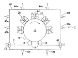
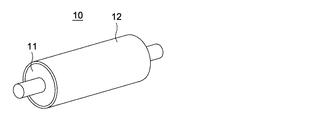
図2は、第1電極10の1例の斜視図であり、この第1電極10は、導電性の金属質母材11の表面に誘電体12が被覆されたロール状電極である。第1電極10の内部には、表面温度を調節するため、例えば、水やシリコンオイル等の温度調節用の媒体が循環できるようになっている。また、第1電極10には、フィルタ(図示せず)を介して第1電源(同)が接続されている。第1電極10の周縁には、基材2を第1電極10の周面に密着させて搬送するために基材用搬送機構15と、基材2上に薄膜を形成するための複数の薄膜形成ユニット20が設けられている。
FIG. 2 is a perspective view of an example of the
基材用搬送機構15には、基材2を第1電極10の周面に案内する第1ガイドローラ16及びニップローラ17と、前記周面に密着した基材2を剥がして、次行程まで案内する第2ガイドローラ18と、第1ガイドローラ16、第2ガイドローラ18及び第1電極10を連動するように回転させる駆動源(図示せず)とが設けられている。
In the base
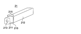
図3は薄膜形成ユニット20の側面図である。薄膜形成ユニット20には、第1電極10の周面に対向し、第1電極10よりも幅の大きい一対の第2電極21A、21Bが、間隔aを空けて配置されている。当該間隔aが放電空間Aであり、放電空間Aを成す第1電極10及び第2電極21の対向する面をそれぞれ放電面10a、21aとする。また、一対の第2電極21の間には、隙間bが設けられている。図4は、第2電極21を表す斜視図であり、第2電極21は導電性の金属質母材211の表面に誘電体212が被覆された棒状電極である。第2電極21は内部が中空となっており、この中空部分213に温度調節用の媒体を流すことにより、電極表面の温度調節ができるようになっている。また、第2電極21の角部(連結角部)215は円弧状に形成されている。つまり、第2電極21の四面は角部215を介して連続していることから、放電面10a及び放電面10a以外の表面も連続することになる。そして、各薄膜形成ユニット20の第2電極21には、第2フィルタ(図示せず)を介して第2電源(同)が接続されている。
FIG. 3 is a side view of the thin
また、薄膜形成ユニット20には、一対の第2電極21の隙間bに向けてガスを噴出するガス供給部24が、前記隙間bに対向するように配置されている。これにより隙間bは、放電空間Aにガスを供給する流路Bとなる。ガス供給部24には、内部にガス流路が形成されたノズル本体部25と、ノズル本体部25から流路Bに向けて突出し、ガス流路に連通してガスを噴出するガス噴出部26とが設けられている。
In the thin
また、薄膜形成ユニット20には、第2電極21の汚れを防止するクリーニングフィルム27を、第2電極21に密着させながら、連続的若しくは間欠的に搬送するフィルム用搬送機構30が各第2電極21毎に設けられている。このフィルム用搬送機構30には、ガス供給部24の近傍で、クリーニングフィルム27を案内する第1フィルム用ガイドローラ31が設けられている。この第1フィルム用ガイドローラ31の上流側には、図示しないクリーニングフィルム27の巻き出しローラ若しくはクリーニングフィルム27の元巻が設けられている。
Further, in the thin
また、ガス供給部24に対して、第1フィルム用ガイドローラ31よりも遠方には、第2フィルム用ガイドローラ32を介してクリーニングフィルム27を巻き取る巻取部(図示省略)が設けられている。第1フィルム用ガイドローラ31、第2フィルム用ガイドローラ32及びクリーニングフィルム27の全幅は、第1電極10の全幅よりも長く設定されている。具体的には、クリーニングフィルム27の全幅長は、両端が第1電極10の両端から1〜100mmではみ出すように設定されていることが好ましい。これにより、クリーニングフィルム27が放電空間Aよりも大きくなる。つまり第2電極21は、クリーニングフィルム27に覆われることにより、放電プラズマに晒されなくなり、第2電極21に対する汚れを防止できる。また、クリーニングフィルム27のエッジが放電空間A内に侵入しないために、放電集中によるアーク放電を防止できる。
Further, a winding unit (not shown) for winding the
このフィルム用搬送機構30によってクリーニングフィルム27は、巻出ローラから引き出された後、第1フィルム用ガイドローラ31に案内されて、ガス供給部24のノズル本体部25の周縁に接触した後に、第2電極21の流路Bを形成する表面21bに密着してから、角部215を介して放電面21aに密着し、第2フィルム用ガイドローラ32に案内されて、巻取部で巻き取られるようになっている。この際、角部215が円弧状に形成されているので、クリーニングフィルム27が前記放電面21a以外の表面21bから放電面21aまで移動する際に引っかかることを防止でき、スムーズに搬送させることができる。なお第2電極21の放電面21aを、第1電極10の放電面10aに向かって凸となる曲面に形成してもよい。こうした場合、小電極21の放電面21aとクリーニングフィルム27との密着性をさらに高めることができる。さらに、流路Bを形成する第2電極21の表面を流路Bの中央に向けて凸となる曲面に形成してもよい。これにより、クリーニングフィルム27を流路B内でも小電極21に密着させながらスムーズに搬送させることができ、皺やツレの発生を抑制することができる。
After the
そして、上記のように、クリーニングフィルム27とノズル本体部25とが接触しているので、ガス供給部24から流路Bまでの空間は、クリーニングフィルム27によって仕切られることになって、ガスが流路B外に流れることを防止できる。
As described above, since the
上述の各電極において、金属質母材としては、例えば、銀、白金、チタン、チタン合金、ステンレス、アルミニウム、鉄等の金属等が挙げられるが、加工の観点からステンレス、チタン、チタン合金であることが好ましい。 In each of the electrodes described above, examples of the metallic base material include metals such as silver, platinum, titanium, titanium alloy, stainless steel, aluminum, and iron, and are stainless steel, titanium, and titanium alloy from the viewpoint of processing. It is preferable.
誘電体は、比誘電率が6〜45の無機化合物であることが好ましく、また、このような誘電体としては、アルミナ、窒化珪素等のセラミックス、あるいは、ケイ酸塩系ガラス、ホウ酸塩系ガラス等のガラスライニング材等がある。この中では、アルミナを溶射して設けた誘電体が好ましい。また必要に応じて封孔処理を行うことが好ましい。 The dielectric is preferably an inorganic compound having a relative dielectric constant of 6 to 45, and examples of such a dielectric include ceramics such as alumina and silicon nitride, silicate glass, and borate. There are glass lining materials such as glass. Among these, a dielectric provided by spraying alumina is preferable. Moreover, it is preferable to perform a sealing process as needed.
対向する電極間の距離(電極間隙)は、導電性の金属質母材に設けた誘電体の厚さ、基板の厚み、印加電圧の大きさ、プラズマを利用する目的等を考慮して決定されるが、電極の一方に誘電体を設けた場合の誘電体表面と導電性の金属質母材表面の最短距離、上記電極の双方に誘電体を設けた場合の誘電体表面同士の距離としては、いずれの場合も均一な放電を行う観点から0.1〜20mmが好ましく、特に好ましくは0.5〜2mmである。 The distance between the opposing electrodes (electrode gap) is determined in consideration of the thickness of the dielectric provided on the conductive metallic base material, the thickness of the substrate, the magnitude of the applied voltage, the purpose of using the plasma, etc. However, the shortest distance between the dielectric surface when a dielectric is provided on one of the electrodes and the surface of the conductive metallic base material, and the distance between the dielectric surfaces when a dielectric is provided on both electrodes In any case, the thickness is preferably 0.1 to 20 mm, particularly preferably 0.5 to 2 mm, from the viewpoint of uniform discharge.
薄膜形成装置1は全体をチャンバ40で囲まれており、基材2の入口部及び出口部は入口側ニップロール41と出口側ニップロール42により外気と遮断されている。なお基材の入口部及び出口部は完全に密閉する必要は無いが、この様な外気遮断手段を設けるのが好ましい。チャンバー壁部には不活性ガス等のパージガスを供給するパージガス供給口43a〜43fが設けられ、ここからパージガスを供給して励起ガスの存在領域での酸素濃度を12%以下とする。44a、44bは排気口だが、薄膜形成ガスや薄膜形成時に発生するパーティクルを排出する電極近傍のノズル(図示せず)が有るので、有ってもなくても良い。またパージガス供給口43及び排気口44の配置や設置個数に特に制限はない。
The thin
なお図示していない電源やフィルタ、駆動源、電極の温度調整用冷却ポンプ等はチャンバの外部にあり、電圧印加には銅板やケーブルを用い、温度調整は配管を用いる形で行う。 A power source, a filter, a drive source, an electrode temperature adjustment cooling pump, etc., not shown, are provided outside the chamber, a voltage is applied using a copper plate or a cable, and temperature adjustment is performed using a pipe.
図5は、本発明の薄膜形成装置の他の実施形態をモデル的に示す図である。 FIG. 5 is a diagram schematically showing another embodiment of the thin film forming apparatus of the present invention.
この実施形態においては、パージガス供給口43がチャンバ40内部に導入される供給管43a’〜43d’により構成される。
In this embodiment, the purge gas supply port 43 is constituted by
以下、実施例にて本発明を説明するが、本発明はこれに限定されるものではない。 EXAMPLES Hereinafter, although an Example demonstrates this invention, this invention is not limited to this.
実施例1
厚さ80μm、幅約1300mmのトリアセテートフィルムに下記組成のハードコート層塗布組成物を3μmの膜厚となるように押出しコーターでコーティングし、ついで80℃で1分間乾燥した後、120mW/cm2で紫外線照射することにより形成した基材に、図1に示す装置を用い、パージガスの供給条件を変えて放電空間近傍の酸素濃度を変化させ、以下に示す条件でて膜厚100nmのTiO2膜の形成を行った。
Example 1
A triacetate film having a thickness of 80 μm and a width of about 1300 mm was coated with a hard coat layer coating composition having the following composition by an extrusion coater to a film thickness of 3 μm, then dried at 80 ° C. for 1 minute, and then 120 mW / cm 2 . The substrate shown in FIG. 1 is used for the base material formed by irradiating with ultraviolet rays, and the oxygen concentration in the vicinity of the discharge space is changed by changing the purge gas supply conditions. Under the conditions shown below, the TiO 2 film having a thickness of 100 nm is formed. Formation was performed.
(クリアハードコート層塗布組成物)
ジぺンタエリスリトールヘキサアクリレート単量体 60質量部
ジぺンタエリスリトールヘキサアクリレート2量体 20質量部
ジぺンタエリスリトールヘキサアクリレート3量体以上の成分 20質量部
ジメトキシベンゾフェノン 4質量部
酢酸エチル 50質量部
メチルエチルケトン 50質量部
イソプロピルアルコール 50質量部
(電極条件)
第1電極10は、チタン合金T64製、直径1000mmのロール形状で、大気プラズマ法により高密度、高密着性のアルミナ溶射膜を被覆後、テトラメトキシシランを酢酸エチルで希釈した溶液を塗布乾燥し、紫外線照射により硬化して封孔処理された誘電体で被覆され、誘電体表面はRmax5μmとなるように研磨処理されている。
(Clear hard coat layer coating composition)
Dipentaerythritol hexaacrylate monomer 60 parts by mass Dipentaerythritol hexaacrylate dimer 20 parts by mass Dipentaerythritol hexaacrylate trimer or
The
第2電極21は、チタン合金T64製、40mm×40mmの略角柱形状で、同様の誘電体で被覆されている。またクリーニングフィルム27としては、三菱化学ポリエステルフィルム社製のポリエチレンテレフタレートを用いた。
The
(ガス条件)
放電ガス :N2 99.4体積%
添加ガス :H2 0.5体積%
薄膜形成ガス:テトライソプロポキシチタン 0.1体積%
(リンテック社製気化器にてアルゴンガスに混合して気化させた)
(印加条件)
第1電極10の電源:100kHz、6W/cm2
第2電極21の電源:13.56MHz、6W/cm2
薄膜形成した基材を搬送方向に直交して1mの短冊にスライスし、任意に選んだ数カ所のサンプルをトータルで10m2として評価サンプルとし、1500ルクス以上の照度条件で、100倍の顕微鏡にて観察し、以下の評価基準でピンホール等の異物の有無を観察して膜面故障の評価を行った。
(Gas condition)
Discharge gas: N 2 99.4% by volume
Additive gas: H 2 0.5% by volume
Thin film forming gas: tetraisopropoxy titanium 0.1% by volume
(The mixture was vaporized by mixing with argon gas with a Lintec vaporizer)
(Apply condition)
Power source of the first electrode 10: 100 kHz, 6 W / cm 2
Power source of the second electrode 21: 13.56 MHz, 6 W / cm 2
The thin film-formed substrate is sliced into 1-m strips perpendicular to the transport direction, and several arbitrarily selected samples are evaluated as 10 m 2 , using a 100 × microscope under an illumination condition of 1500 lux or more. The film surface failure was evaluated by observing and observing the presence or absence of foreign matter such as pinholes according to the following evaluation criteria.
膜面故障評価基準
◎:評価サンプル中に欠陥となる異物が観察されない
○:50μm以上の異物が0.1個/m2未満である
△:50μm以上の異物が0.1個/m2以上存在する
×:100μm以上の異物が1個/m2以上存在する
以上の結果を表1に示す。
Evaluation criteria for film surface failure ◎: No foreign matter that becomes a defect is observed in the evaluation sample ○: Foreign matter of 50 μm or more is less than 0.1 / m 2 Δ: Foreign matter of 50 μm or more is 0.1 / m 2 or more Existence x: Foreign matter of 100 μm or more is present 1 / m 2 or more Table 1 shows the above results.

これにより、本発明の薄膜形成装置を用い、酸素濃度を12%以下とすれば、著しくパーティクルの発生を抑制できることが解る。 Thus, it can be seen that if the thin film forming apparatus of the present invention is used and the oxygen concentration is 12% or less, the generation of particles can be remarkably suppressed.
1 薄膜形成装置
2 基材
10 第1電極
15 基材用搬送機構
20 薄膜形成ユニット
21 第2電極
24 ガス供給部
27 クリーニングフィルム
30 フィルム用搬送機構
40 チャンバ
43 パージガス供給口
44 排気口
DESCRIPTION OF
Claims (17)
少なくとも前記励起ガスの存在領域での酸素濃度の制御手段を有することを特徴とする薄膜形成装置。 In a thin film forming apparatus for generating a discharge plasma by applying a high frequency voltage between opposing electrodes, exciting a gas containing a thin film forming gas and exposing the base material to form a thin film on the base material,
A thin film forming apparatus comprising a control means for oxygen concentration at least in a region where the excitation gas exists.
少なくとも前記励起ガスの存在領域での酸素濃度を制御することを特徴とする薄膜形成方法。 In a thin film forming method for generating a discharge plasma by applying a high-frequency voltage between opposing electrodes, exciting a gas containing a thin film forming gas and exposing the substrate to form a thin film on the substrate,
A method for forming a thin film, comprising controlling an oxygen concentration at least in a region where the excitation gas exists.
Priority Applications (1)
| Application Number | Priority Date | Filing Date | Title |
|---|---|---|---|
| JP2004110767A JP2005290522A (en) | 2004-04-05 | 2004-04-05 | Method for forming thin film and apparatus used therefor |
Applications Claiming Priority (1)
| Application Number | Priority Date | Filing Date | Title |
|---|---|---|---|
| JP2004110767A JP2005290522A (en) | 2004-04-05 | 2004-04-05 | Method for forming thin film and apparatus used therefor |
Publications (1)
| Publication Number | Publication Date |
|---|---|
| JP2005290522A true JP2005290522A (en) | 2005-10-20 |
Family
ID=35323784
Family Applications (1)
| Application Number | Title | Priority Date | Filing Date |
|---|---|---|---|
| JP2004110767A Pending JP2005290522A (en) | 2004-04-05 | 2004-04-05 | Method for forming thin film and apparatus used therefor |
Country Status (1)
| Country | Link |
|---|---|
| JP (1) | JP2005290522A (en) |
-
2004
- 2004-04-05 JP JP2004110767A patent/JP2005290522A/en active Pending
Similar Documents
| Publication | Publication Date | Title |
|---|---|---|
| KR100296692B1 (en) | Plasma CVD | |
| CN110168130B (en) | Film forming method and roll-to-roll film forming apparatus | |
| CN103215573B (en) | Vacuum film formation apparatus | |
| WO2011043047A1 (en) | Plasma cvd device | |
| JP2013503974A (en) | Plasma chemical vapor deposition equipment | |
| JP4747658B2 (en) | Film forming apparatus and film forming method | |
| JP2009280873A (en) | Method for producing gas barrier film | |
| JP4747665B2 (en) | Film forming apparatus and film forming method | |
| JPWO2010100971A1 (en) | Substrate having a thin film | |
| WO2008047549A1 (en) | Transparent conductive film substrate and method of forming titanium oxide based transparent conductive film for use therein | |
| JP3518977B2 (en) | Plasma CVD equipment | |
| JP4597756B2 (en) | Film forming apparatus and film forming method | |
| JP4601385B2 (en) | Pressure gradient ion plating film deposition system | |
| JP2005290522A (en) | Method for forming thin film and apparatus used therefor | |
| JP4601387B2 (en) | Pressure gradient ion plating film deposition system | |
| JP4613048B2 (en) | Pressure gradient ion plating film deposition system | |
| JP3519046B2 (en) | Plasma CVD equipment | |
| JP4613056B2 (en) | Pressure gradient ion plating film forming apparatus and film forming method | |
| JP4019712B2 (en) | Plasma discharge treatment apparatus and plasma discharge treatment method | |
| JP2011179084A (en) | Atmospheric plasma apparatus | |
| JP2004323928A (en) | Atmospheric pressure plasma treatment method, and system used therefor | |
| WO2009104579A1 (en) | Plasma discharge device and thin film laminate | |
| JP2003055771A (en) | Plasma processing apparatus and processing method | |
| WO2016080447A1 (en) | Film formation device and gas barrier film-manufacturing method | |
| JP2004162136A (en) | Plasma discharge treatment method |