JP2005290510A - Electron beam vapor deposition method and apparatus therefor - Google Patents
Electron beam vapor deposition method and apparatus therefor Download PDFInfo
- Publication number
- JP2005290510A JP2005290510A JP2004109932A JP2004109932A JP2005290510A JP 2005290510 A JP2005290510 A JP 2005290510A JP 2004109932 A JP2004109932 A JP 2004109932A JP 2004109932 A JP2004109932 A JP 2004109932A JP 2005290510 A JP2005290510 A JP 2005290510A
- Authority
- JP
- Japan
- Prior art keywords
- electron beam
- anode
- cathode
- vapor deposition
- pulse
- Prior art date
- Legal status (The legal status is an assumption and is not a legal conclusion. Google has not performed a legal analysis and makes no representation as to the accuracy of the status listed.)
- Pending
Links
- 238000010894 electron beam technology Methods 0.000 title claims abstract description 96
- 238000007740 vapor deposition Methods 0.000 title claims abstract description 37
- 238000000034 method Methods 0.000 title claims abstract description 23
- 239000000463 material Substances 0.000 claims abstract description 85
- 238000001704 evaporation Methods 0.000 claims abstract description 84
- 230000008020 evaporation Effects 0.000 claims abstract description 46
- 239000000758 substrate Substances 0.000 claims abstract description 34
- 239000002344 surface layer Substances 0.000 claims abstract description 12
- 230000001133 acceleration Effects 0.000 claims description 16
- 238000005566 electron beam evaporation Methods 0.000 claims description 12
- 229910052751 metal Inorganic materials 0.000 claims description 10
- 239000002184 metal Substances 0.000 claims description 10
- 238000009434 installation Methods 0.000 claims description 9
- RTAQQCXQSZGOHL-UHFFFAOYSA-N Titanium Chemical compound [Ti] RTAQQCXQSZGOHL-UHFFFAOYSA-N 0.000 claims description 8
- 230000008859 change Effects 0.000 claims description 7
- 230000005284 excitation Effects 0.000 claims description 7
- 239000010936 titanium Substances 0.000 claims description 7
- 229910052719 titanium Inorganic materials 0.000 claims description 7
- 229910000975 Carbon steel Inorganic materials 0.000 claims description 6
- 239000010962 carbon steel Substances 0.000 claims description 6
- 238000000313 electron-beam-induced deposition Methods 0.000 claims description 4
- 229910052756 noble gas Inorganic materials 0.000 claims description 4
- 238000000151 deposition Methods 0.000 abstract description 16
- 230000001678 irradiating effect Effects 0.000 abstract description 2
- 239000007789 gas Substances 0.000 description 27
- 230000008021 deposition Effects 0.000 description 15
- 150000002500 ions Chemical class 0.000 description 14
- 230000005684 electric field Effects 0.000 description 12
- 230000015572 biosynthetic process Effects 0.000 description 9
- 239000003990 capacitor Substances 0.000 description 9
- XEEYBQQBJWHFJM-UHFFFAOYSA-N Iron Chemical compound [Fe] XEEYBQQBJWHFJM-UHFFFAOYSA-N 0.000 description 8
- 230000004048 modification Effects 0.000 description 7
- 238000012986 modification Methods 0.000 description 7
- 238000010438 heat treatment Methods 0.000 description 6
- 238000005516 engineering process Methods 0.000 description 5
- 238000001816 cooling Methods 0.000 description 4
- 229910052742 iron Inorganic materials 0.000 description 4
- 238000003754 machining Methods 0.000 description 4
- 239000002245 particle Substances 0.000 description 4
- RYGMFSIKBFXOCR-UHFFFAOYSA-N Copper Chemical compound [Cu] RYGMFSIKBFXOCR-UHFFFAOYSA-N 0.000 description 3
- 229910000881 Cu alloy Inorganic materials 0.000 description 3
- 239000000956 alloy Substances 0.000 description 3
- 239000011248 coating agent Substances 0.000 description 3
- 238000000576 coating method Methods 0.000 description 3
- 239000010949 copper Substances 0.000 description 3
- 229910052802 copper Inorganic materials 0.000 description 3
- 230000008569 process Effects 0.000 description 3
- 239000000126 substance Substances 0.000 description 3
- XKRFYHLGVUSROY-UHFFFAOYSA-N Argon Chemical compound [Ar] XKRFYHLGVUSROY-UHFFFAOYSA-N 0.000 description 2
- OKTJSMMVPCPJKN-UHFFFAOYSA-N Carbon Chemical compound [C] OKTJSMMVPCPJKN-UHFFFAOYSA-N 0.000 description 2
- PXHVJJICTQNCMI-UHFFFAOYSA-N Nickel Chemical compound [Ni] PXHVJJICTQNCMI-UHFFFAOYSA-N 0.000 description 2
- 239000000919 ceramic Substances 0.000 description 2
- 238000000354 decomposition reaction Methods 0.000 description 2
- 230000000694 effects Effects 0.000 description 2
- 230000035515 penetration Effects 0.000 description 2
- 238000003672 processing method Methods 0.000 description 2
- 230000000644 propagated effect Effects 0.000 description 2
- 230000003746 surface roughness Effects 0.000 description 2
- PZNSFCLAULLKQX-UHFFFAOYSA-N Boron nitride Chemical compound N#B PZNSFCLAULLKQX-UHFFFAOYSA-N 0.000 description 1
- ZOKXTWBITQBERF-UHFFFAOYSA-N Molybdenum Chemical compound [Mo] ZOKXTWBITQBERF-UHFFFAOYSA-N 0.000 description 1
- XUIMIQQOPSSXEZ-UHFFFAOYSA-N Silicon Chemical compound [Si] XUIMIQQOPSSXEZ-UHFFFAOYSA-N 0.000 description 1
- 230000003213 activating effect Effects 0.000 description 1
- 229910045601 alloy Inorganic materials 0.000 description 1
- 229910052786 argon Inorganic materials 0.000 description 1
- 229910052799 carbon Inorganic materials 0.000 description 1
- 239000002131 composite material Substances 0.000 description 1
- 150000001875 compounds Chemical class 0.000 description 1
- 238000011109 contamination Methods 0.000 description 1
- 230000008878 coupling Effects 0.000 description 1
- 238000010168 coupling process Methods 0.000 description 1
- 238000005859 coupling reaction Methods 0.000 description 1
- 238000005520 cutting process Methods 0.000 description 1
- 230000007423 decrease Effects 0.000 description 1
- 230000003111 delayed effect Effects 0.000 description 1
- 210000004513 dentition Anatomy 0.000 description 1
- 238000010586 diagram Methods 0.000 description 1
- 238000009792 diffusion process Methods 0.000 description 1
- 238000009826 distribution Methods 0.000 description 1
- 238000010893 electron trap Methods 0.000 description 1
- 239000010419 fine particle Substances 0.000 description 1
- 229910002804 graphite Inorganic materials 0.000 description 1
- 239000010439 graphite Substances 0.000 description 1
- 230000003760 hair shine Effects 0.000 description 1
- 239000012212 insulator Substances 0.000 description 1
- 238000007733 ion plating Methods 0.000 description 1
- 238000010884 ion-beam technique Methods 0.000 description 1
- 238000000608 laser ablation Methods 0.000 description 1
- 230000007246 mechanism Effects 0.000 description 1
- 230000008018 melting Effects 0.000 description 1
- 238000002844 melting Methods 0.000 description 1
- 229910001092 metal group alloy Inorganic materials 0.000 description 1
- 239000007769 metal material Substances 0.000 description 1
- 150000002739 metals Chemical class 0.000 description 1
- 239000000203 mixture Substances 0.000 description 1
- 229910052750 molybdenum Inorganic materials 0.000 description 1
- 239000011733 molybdenum Substances 0.000 description 1
- 229910052759 nickel Inorganic materials 0.000 description 1
- 229910052755 nonmetal Inorganic materials 0.000 description 1
- 150000002843 nonmetals Chemical class 0.000 description 1
- 230000000704 physical effect Effects 0.000 description 1
- 238000002360 preparation method Methods 0.000 description 1
- 230000006798 recombination Effects 0.000 description 1
- 238000005215 recombination Methods 0.000 description 1
- 239000003870 refractory metal Substances 0.000 description 1
- 230000001105 regulatory effect Effects 0.000 description 1
- 230000004044 response Effects 0.000 description 1
- 239000010703 silicon Substances 0.000 description 1
- 229910052710 silicon Inorganic materials 0.000 description 1
- 238000004544 sputter deposition Methods 0.000 description 1
- 238000000859 sublimation Methods 0.000 description 1
- 230000008022 sublimation Effects 0.000 description 1
- 238000004381 surface treatment Methods 0.000 description 1
- 230000036346 tooth eruption Effects 0.000 description 1
- WFKWXMTUELFFGS-UHFFFAOYSA-N tungsten Chemical compound [W] WFKWXMTUELFFGS-UHFFFAOYSA-N 0.000 description 1
- 229910052721 tungsten Inorganic materials 0.000 description 1
- 239000010937 tungsten Substances 0.000 description 1
- 238000001771 vacuum deposition Methods 0.000 description 1
Images
Landscapes
- Physical Vapour Deposition (AREA)
Abstract
Description
本発明は、特殊な電子ビームを熱源として用いる主として金属合金の、各種のサブストレイト(基板、基体)表面に対する真空蒸着方法及び装置に関し、従来慣用の所謂電子ビーム蒸着方法及び装置と対比して、蒸着速度が格段に早く、また高融点金属の蒸着に適用して有用なものである。 The present invention relates to a vacuum deposition method and apparatus for various substrate (substrate, substrate) surfaces of mainly metal alloys using a special electron beam as a heat source, and in contrast to the so-called conventional electron beam deposition method and apparatus, The deposition rate is remarkably fast, and it is useful when applied to the deposition of refractory metals.
前述従来慣用の電子ビーム蒸着は、数KV以上で加速された電子線をターゲット(蒸着用材料)に照射し、電子の運動エネルギを熱に変える加熱方法を利用するものである。そして、このものは、熱電子源が蒸発物質で汚されるのを防ぐため、電子線は磁界で180〜270°に曲げられ、蒸発材料に集束させられるように構成されているものである。前記蒸発材料は、細く絞られた電子線によって、局所的に、かつ直接加熱できるので、蒸気圧の低い材料の蒸着も容易で、汎用性が高いものである。 The conventional electron beam vapor deposition as described above uses a heating method in which an electron beam accelerated at several KV or more is irradiated onto a target (deposition material) and the kinetic energy of electrons is changed to heat. And this thing is comprised so that an electron beam may be bent by 180-270 degrees with a magnetic field, and it may be made to focus on evaporation material, in order to prevent that a thermal electron source is polluted with an evaporation substance. Since the evaporating material can be heated locally and directly by a narrowed electron beam, it is easy to deposit a material having a low vapor pressure and is highly versatile.
そして、絶縁体の蒸発材料上への電子線の集束も比較的容易であることから好適なものであるが、高融点物質や昇華性物質あるいは熱伝導の悪い材料の場合には、電子線の当たった部分だけが蒸発して穴が明くので、電子線を蒸発材上で走査させる機構が必要になる。また。蒸発材料は、銅製の水冷ハ−スの上に直接おいてもよいが(蒸発材料と反応しない限り)、黒鉛、窒化ほう素(BN)系コンポジット材、Taなどでできた受皿を敷くと、蒸発材料の交換が容易になるし、熱の伝導損失が減り、蒸発溶湯部分の面積を大きくできるものである(例えば、非特許文献1参照。)。 The focusing of the electron beam on the evaporation material of the insulator is relatively easy, but it is preferable. However, in the case of a high melting point substance, a sublimation substance or a material having poor heat conduction, Since only the contact portion evaporates and a hole is formed, a mechanism for scanning the electron beam on the evaporation material is required. Also. The evaporating material may be placed directly on a copper water-cooled hearth (unless it reacts with the evaporating material), but when a tray made of graphite, boron nitride (BN) composite material, Ta or the like is laid, Exchange of the evaporation material is facilitated, heat conduction loss is reduced, and the area of the evaporation molten metal portion can be increased (for example, see Non-Patent Document 1).
そして、之等の電子ビーム蒸着は、膜形成の蒸着速度が必ずしも高くないにもかかわらず、設備費が高く、操作性も良くないところから、高度に発達したエレクトロニクス分野の微細な各種の電子デバイスの成膜技術として、或いは費用などを無視し得る原子力やミサイル等の軍事用等に用いられるものの、近時はスパッタリングやイオンプレーティング、及びレーザアブレーション(パルスレーザデポジション)などの技術に、その場を奪われつつあるものである(例えば、非特許文献2参照。)。 In addition, the electron beam evaporation method of this group has a high equipment cost and a poor operability even though the film formation evaporation rate is not always high. Although it is used as a film deposition technology or for military applications such as nuclear power and missiles where costs can be ignored, recently it has been applied to technologies such as sputtering, ion plating, and laser ablation (pulse laser deposition). The place is being deprived (see, for example, Non-Patent Document 2).
ところで、近時、金属義歯や炭素鋼から成る金型の機械切削、研削仕上げ面、或いはワイヤ放電加工を含む放電加工面の仕上げ等に、照射軸方向と直角方向の断面の径がφ60mmまたはそれ以上と言う照射面積の大きい大面積の電子ビームのパルスを繰り返し照射して、それらの仕上面を短時間で一挙に仕上げる表面改質加工方法及び装置が知られるようになって来た(例えば、特許文献1−3、及び非特許文献3参照。)。
By the way, recently, the diameter of the cross section in the direction perpendicular to the irradiation axis direction is φ60 mm or more for mechanical cutting of metal dentition or die made of carbon steel, finishing of the ground surface, or electric discharge machining surface including wire electric discharge machining. Surface modification processing methods and apparatuses that repeatedly irradiate a large-area electron beam pulse with a large irradiation area and finish their finished surfaces in a short time have come to be known (for example, (See Patent Literatures 1-3 and
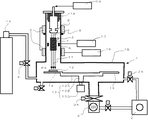
以下この表面改質加工方法及び装置の一例を説明するに、図3は、全体構成の概略を示す装置断面図で、1は真空ハウジング、6は環状アノード、8は大面積カソード、Sは電子加速空間、5は上下ソレノイドコイルから成る磁場付与手段、14はビームコレクタを示している。前記真空ハウジング1は、電子ビーム発生部を収納する筒状のビームハウジング部1Aと、電子ビームの照射を受けるコレクタ14等を収納する加工処理ハウジング部1Bとから成り、前記ビームハウジング部1Aは電子ビームを上下鉛直方向に照射するように設置されるのに対し、加工処理ハウジング部1Bは、コレクタ14上のワーク12を、鉛直照射電子ビーム11に対して直交する水平方向に移動又は送り位置決めし得るように回転台13又は直線1軸若しくは直交2軸のテーブルに取り付け収設している。
Hereinafter, an example of the surface modification processing method and apparatus will be described. FIG. 3 is an apparatus cross-sectional view showing an outline of the overall configuration. 1 is a vacuum housing, 6 is an annular anode, 8 is a large area cathode, and S is an electron. Acceleration space, 5 is a magnetic field applying means comprising upper and lower solenoid coils, and 14 is a beam collector. The vacuum housing 1 includes a cylindrical beam housing portion 1A that houses an electron beam generating portion, and a processing housing portion 1B that houses a collector 14 and the like that receive electron beam irradiation. The beam housing portion 1A is an electron housing. The processing housing portion 1B moves or feeds the workpiece 12 on the collector 14 in the horizontal direction perpendicular to the vertical irradiation electron beam 11 while being installed so as to irradiate the beam in the vertical direction. In order to obtain it, it is attached to the
前記回転台13は廻りにコレクタ14を取り付けた円形板13Aと、該円形板13Aを加工処理ハウジング部1Bに取り付け支持する回転支柱13Bと、加工処理ハウジング部1B壁に気密に取り付けられた回転支柱13Bを外部で回転駆動するように設けた回転モータ13Cを有し、所要のコレクタ14の載置ワーク12を電子ビーム11の照射を受ける加工処理ポジションPAに位置させることが出来るように構成されている。 The rotary table 13 includes a circular plate 13A around which a collector 14 is attached, a rotary column 13B that attaches and supports the circular plate 13A to the processing housing part 1B, and a rotary column that is airtightly attached to the wall of the processing housing part 1B. A rotary motor 13C is provided so as to drive the rotation of 13B externally, and is configured so that the work 12 mounted on the required collector 14 can be positioned at the processing position PA where the electron beam 11 is irradiated. Yes.
前記真空ハウジング1には、スクロールポンプ2とターボ分子ポンプ3とが夫々流量調節弁2A、3Aを介して連結され、さらに、アルゴン(Ar)等のガスボンベ15を、図示しない真空ハウジング部1に設置の真空センサによる検出ガス圧が、設定ガス圧となるよう制御される圧力調整弁4を介して連結することにより、真空ハウジング部1内は、一旦1×10⁻²Pa以下の真空状態とした後、例えば、0.3〜0.5×10⁻¹Pa程度の所定の低ガス圧状態に保たれる。
A
この図3の加工処理装置には、図3〜4で図示説明するように3つの、通常コンデンサ使用のパルス電源が設けられる。先ず第1のパルス電源16は、カソード8とアノード6及びコレクタ14間の陽極プラズマ7形成を伴う低圧ガス中放電を、カソード8とアノード6が対向する電子加速空間S内に安定的に閉じ込めた状態で行われるように、図5に示す磁場空間を前記電子加速空間Sを取り囲んだ状態に形成する電子ビーム照射軸方向に複数個設けられるソレノイド5、5励磁用コンデンサ充放電パルス電源で、具体的には、例えば、約1000μFのコンデンサを約1〜2KVに充電し、約100〜200Aの放電ピーク電流で、約10〜20msのパルス幅で放電させて前記閉じ込め磁場、例えば、4.4KOeを発生形成させるよう、環状アノード6は、上下のソレノイド5、5の間に位置する。
The processing apparatus shown in FIG. 3 is provided with three pulse power supplies using ordinary capacitors as shown in FIGS. First, the first pulse power supply 16 stably traps the discharge in the low-pressure gas accompanied by the formation of the anode plasma 7 between the cathode 8 and the anode 6 and the collector 14 in the electron acceleration space S where the cathode 8 and the anode 6 face each other. As shown in FIG. 5, the magnetic field space shown in FIG. 5 is formed so as to surround the electron acceleration space S. Specifically, for example, a capacitor of about 1000 μF is charged to about 1 to 2 KV and discharged at a discharge peak current of about 100 to 200 A and a pulse width of about 10 to 20 ms, so that the confined magnetic field, for example, 4.4 KO e is used. The annular anode 6 is positioned between the upper and
次に第2のパルス電源17は、カソード8とアノード6及びコレクタ14に印加されて前記閉じ込め磁場が形成されている電子加速空間Sの領域に低圧ガス電離の陽極プラズマ形成を伴う低圧ガス放電、グロー放電を生成させるコンデンサ充放電パルスで、具体的には、例えば、約5μFのコンデンサを約4〜5KVに充電し、約50〜150Aの放電ピーク電流で、約10〜100μsのパルス幅で、前記第1のパルス電源のスイッチ・オンによる放電開始後約20μs〜5ms遅延させて、充分な磁場形成を待って放電のスイッチ・オンにして、前記陽極プラズマ7形成を伴う低圧ガスグロー放電を生じさせるパルス電源である。 Next, the second pulse power source 17 is applied to the cathode 8, the anode 6 and the collector 14, and the low pressure gas discharge accompanied by the anode plasma formation of the low pressure gas ionization in the region of the electron acceleration space S in which the confinement magnetic field is formed. Capacitor charge / discharge pulses for generating glow discharge, specifically, for example, a capacitor of about 5 μF is charged to about 4 to 5 KV, a discharge peak current of about 50 to 150 A, and a pulse width of about 10 to 100 μs, A delay of about 20 .mu.s to 5 ms after the start of discharge by switching on of the first pulse power supply, waiting for a sufficient magnetic field formation to switch on the discharge, thereby generating a low-pressure gas glow discharge accompanied with the formation of the anode plasma 7. It is a pulse power supply.
そして、第3のパルス電源18は、前述第1のパルス電源16及び第2のパルス電源17により、閉じ込め磁場中での陽極プラズマ7の形成を伴う低圧ガス放電領域から、大面積のエネルギ密度が適度に高い電子ビーム11の短いパルスを発生照射させるために、立ち上がりが、例えば、約5〜10nsの立ち上がり時間の短いパルス、具体的には、例えば、約3μFのコンデンサを約20〜60KVに充電し、約5〜25KAの放電ピーク電流で、約1〜4μsの極めて短いパルス幅で、前記第2のパルス電源のスイッチ・オンによる放電開始後約10〜100μs遅延させて、前記低圧ガス放電が発生したのを待ってスイッチ・オンすることにより、カソード8に高い立ち上がりの負の高電圧パルスを印加し、アノード6からのイオンビームによってカソード8表面に高密度のカソードプラズマを形成させ、該高密度のカソードプラズマとカソード8からの電子とにより生成する高密度の電子ビーム11を陽極プラズマ7を通じて、アノード6の環内を通り、コレクタ14に照射されることになるのである。 The third pulse power source 18 has a large area energy density from the low-pressure gas discharge region accompanied by the formation of the anode plasma 7 in the confined magnetic field by the first pulse power source 16 and the second pulse power source 17. In order to generate and irradiate a short pulse of a moderately high electron beam 11, the rise is, for example, a pulse with a short rise time of about 5 to 10 ns, specifically, for example, a capacitor of about 3 μF is charged to about 20 to 60 KV The low-pressure gas discharge is delayed by about 10 to 100 μs after the start of discharge by switching on the second pulse power supply with a very short pulse width of about 1 to 4 μs at a discharge peak current of about 5 to 25 KA. By switching on after waiting for the occurrence, a high negative high voltage pulse is applied to the cathode 8, and the ion beam from the anode 6 is applied. To form a high-density cathode plasma on the surface of the cathode 8, and pass a high-density electron beam 11 generated by the high-density cathode plasma and electrons from the cathode 8 through the anode plasma 7 through the ring of the anode 6, The collector 14 is irradiated.
このような、大面積のパルス電子ビーム11の、照射による金属材の表面仕上げ、及び/または表面の改質加工には、前記電子ビーム11のエネルギ密度が約0.1〜10J/cm2程度で、継続照射時間が数μs以内の短いものであるから、ワーク12の表面の電子ビーム照射領域に対して、所定複数回繰り返し照射する場合や、ワーク12表面の電子ビーム11の径よりも大きい領域を順次にスキャンニングして加工等をする場合には、前記第1乃至第3の各パルス電源16〜18を再充電してパルス電子ビームの発生、照射を繰り返えさせる必要があるもので、上述のような電源構成の場合、加工処理の目的、効果から約5〜10s毎又はそれより短い時間間隔で繰り返し照射し得る仕様とすることが望ましいものである。 For such surface finishing and / or surface modification of the metal material by irradiation of the large-area pulsed electron beam 11, the energy density of the electron beam 11 is about 0.1 to 10 J / cm 2. Since the continuous irradiation time is short within a few μs, the electron beam irradiation region on the surface of the workpiece 12 is repeatedly irradiated a predetermined number of times or larger than the diameter of the electron beam 11 on the surface of the workpiece 12. When processing is performed by sequentially scanning an area, it is necessary to recharge each of the first to third pulse power supplies 16 to 18 to repeat generation and irradiation of a pulsed electron beam. Therefore, in the case of the power supply configuration as described above, it is desirable that the specifications be such that the irradiation can be repeatedly performed at intervals of about 5 to 10 s or shorter than that in view of the purpose and effect of the processing.
以上の構成によれば、前述第2の電源17はパルス電源で、アノード6及びカソード8間に対する電圧印加による電界は常時ではなく、また熱電子などの積極的な供給はないので、電圧印加時の上述プラズマ形成は容易でないが、このため第2の電源17によるアノード6及びカソード8間電圧印加に先だって、第1のパルス電源16によるソレノイド5、5の励磁による磁場を生成作用させ、低圧ガス中に存在する自然電子を回転させて電子加速空間S内から逃げ出さないようにするのである。なお、第2のパルス電源17によるパルス電圧印加時に、電離を起動させるための初期荷電粒子の発生には、(1)チタン材などから成るカソード8の微小な突起物の電界集中を利用する、(2)カソード8を加熱して熱電子を放出させる、(3)紫外線など光を照射して光電子を作る、(4)別の粒子源で荷電粒子を発生させておいて注入するなどの補助的手段を付設作動させるようにしてもよい。
According to the above configuration, the second power source 17 is a pulse power source, and the electric field due to voltage application between the anode 6 and the cathode 8 is not always, and there is no active supply of thermoelectrons. The above plasma formation is not easy, but for this reason, prior to the voltage application between the anode 6 and the cathode 8 by the second power source 17, a magnetic field is generated by the excitation of the
ここで、前記作用磁場が、コンデンサの放電が進んでほぼ最大となったところで、アノード6及びカソード8間に第2のパルス電源17からアノード電圧を印加すると、磁場中に補足されている電子は螺旋を描くことによりガス分子との衝突の頻度が大きくなって進行し、ガス分子と衝突して電離し、発生した電子と正イオンとは、夫々反対方向に移動して電離を繰り返す。このとき電子は速やかにアノード6及びカソード8間を通過するのに対し、正イオンは移動度が小さいので短い時間の間には一部以上が残留し、電界の歪みが生じる。即ち、カソード8の周辺に正イオンが多くなり、それがカソード8側の電界を強め放電を進展させる傾向をもつ。正イオンが電子に対し過剰に多くなれば、アノード6及びカソード8間に電位差が生じ、アノード6に向かう電子はそこでトラップ(捕捉)されるようになる。その結果アノード6の近くにアノードプラズマ7が生成し、電子トラップを解消しながらカソード8側へ成長する。 Here, when the anode magnetic field is applied from the second pulse power source 17 between the anode 6 and the cathode 8 when the working magnetic field becomes substantially maximum as the discharge of the capacitor progresses, the electrons captured in the magnetic field are By drawing a spiral, the frequency of collision with gas molecules increases and ionizes by colliding with gas molecules, and the generated electrons and positive ions move in opposite directions and repeat ionization. At this time, electrons quickly pass between the anode 6 and the cathode 8, whereas positive ions have a low mobility, so that some or more remain in a short time, resulting in distortion of the electric field. That is, the number of positive ions increases around the cathode 8, which tends to strengthen the electric field on the cathode 8 side and advance the discharge. If the positive ions are excessive with respect to the electrons, a potential difference is generated between the anode 6 and the cathode 8, and the electrons directed to the anode 6 are trapped there. As a result, anode plasma 7 is generated near the anode 6 and grows toward the cathode 8 while eliminating the electron trap.
アノードプラズマ7部分では、正イオンと電子の密度がほぼ同じであるから、空間電荷電界は殆どなく極めて低い一様な電界で電子流をアノード6に運ぶ状態にある。之に対し、カソード8周辺では、電離によって必要な電子流を作ると同時に急峻な電界を作るのに必要な正イオンの蓄積が起こる。それらの正イオンは電離によって生じた正イオンとアノード6側から流れ込む正イオンとからなり、正イオンはカソード電極8に衝突し、電極から電子を叩き出す。それらの電子はガス分子と衝突して電離させ、之が次々と繰り返されることにより、一次電子、二次電子、三次・・・、の電子が生じる。 In the anode plasma 7 portion, the positive ions and the electron density are almost the same, so there is almost no space charge electric field, and the electron flow is carried to the anode 6 by a very low uniform electric field. On the other hand, in the vicinity of the cathode 8, positive ions necessary for creating a steep electric field at the same time as creating an electron flow necessary by ionization occur. These positive ions consist of positive ions generated by ionization and positive ions flowing from the anode 6 side. The positive ions collide with the cathode electrode 8 and knock out electrons from the electrode. These electrons collide with gas molecules and ionize them, and these electrons are repeated one after another, thereby generating primary electrons, secondary electrons, tertiary, and so on.
このようにして、十分電子が増殖されて正イオンとほぼ同量となる部分にカソードプラズマ9が形成され、急峻な電界を維持するためのバッファ作用の効果をもち、アノードプラズマ7とカソードプラズマ9との中間では僅かに電界は上昇し、再結合を防ぐ役割と消散する荷電粒子を補うために僅かに電離を起こす役割をする。即ち、カソード8周辺の強い電界の部分で、電子が発生・増殖され、カソードプラズマ9とアノードプラズマ7は導電性の良い電子の通路を形成しているものと考えられる。 In this way, the cathode plasma 9 is formed in a portion where electrons are sufficiently propagated and become approximately the same amount as the positive ions, and has the effect of a buffer function for maintaining a steep electric field. The anode plasma 7 and the cathode plasma 9 In the middle, the electric field rises slightly, and serves to prevent recombination and to slightly ionize to compensate for dissipated charged particles. That is, it is considered that electrons are generated and propagated in the portion of the strong electric field around the cathode 8, and the cathode plasma 9 and the anode plasma 7 form a passage of electrons having good conductivity.
この状態になったとき、前述した5〜10nsと言う短い立ち上がり時間で高い負の電圧(50〜60KV)の短い持続時間(1〜5μsのパルス電圧を印加してカソード電位を深い負電位に下げると、カソード8の周辺電界はより急峻となり、電離による電子・イオンは爆的に増殖し、カソードプラズマ9及びアノードプラズマ7を通る大きいエネルギ密度(少なくとも0.1〜1.0J/cm2以上)の面積広がりを持った電子流が、環状アノード6を通りコレクタ14上のワーク12に照射されることになる。 In this state, the cathode potential is lowered to a deep negative potential by applying a pulse voltage of 1 to 5 μs with a short duration (1 to 5 μs) of a high negative voltage (50 to 60 KV) with a short rise time of 5 to 10 ns described above. Then, the electric field around the cathode 8 becomes steeper, and electrons and ions due to ionization proliferate explosively, and a large energy density (at least 0.1 to 1.0 J / cm 2 or more) passing through the cathode plasma 9 and the anode plasma 7. The electron flow having a wide area is irradiated onto the work 12 on the collector 14 through the annular anode 6.
この電子ビームの照射時間は、加工処理ワーク12の表面改質の物理的(物性的)条件から決まって来る因子で、これはワーク12材料の硬さと電子のエネルギ(KV)によって決まる電子が材料の内部へ侵入する深さと材料の熱伝導度とによる。なお、以上は、材料の表面を急速加熱した後急速冷却する手法で表面をアモルファス化して加工改質処理する場合を想定した場合であって、一般に軽い金属や熱伝導の良い金属は、電子ビーム照射時間を短くするものである。 The irradiation time of the electron beam is a factor determined from the physical (physical properties) conditions of the surface modification of the workpiece 12 to be processed. This is because the electron determined by the hardness of the workpiece 12 and the electron energy (KV) is the material. Depends on the depth of penetration of the material and the thermal conductivity of the material. Note that the above is a case where the surface of the material is amorphized by a method of rapidly heating the surface of the material and then rapidly cooling. In general, a light metal or a metal with good heat conduction is an electron beam. It shortens the irradiation time.
このような断面が大面積の電子ビームのエネルギの分布密度を一様にするには、カソード8周辺の電界が一様であることが重要で、そのためにはカソードプラズマ9及びアノードプラズマ7を一様に形成しなければならず、そのためには、プラズマを均一に閉じ込める磁場の方式、形成が重要になる。放電空間が低ガス圧力(約1Pa以下)では、電子の平均自由行程が長くなり、電離のための衝突の機会が減少するので、プラズマの生成、維持は困難になる。これを可能にする方法として前述磁場を用いいる方法がプラズマの閉じ込めに有効である所から、プラズマの生成、維持には有用であるが、プラズマの均一化には必ずしも有効でない。即ち、例えば、磁場強度を強くすると、電子は中心部に集中することになり、断面が大面積のプラズマを均一化することは難しい。 In order to make the energy distribution density of an electron beam having a large cross section uniform, it is important that the electric field around the cathode 8 is uniform. For this purpose, the cathode plasma 9 and the anode plasma 7 are combined. For this purpose, it is important to form and form a magnetic field for uniformly confining plasma. When the discharge space is at a low gas pressure (about 1 Pa or less), the mean free path of electrons becomes long, and the chance of collision for ionization decreases, so that it is difficult to generate and maintain plasma. As a method for enabling this, since the method using the magnetic field is effective for confining the plasma, it is useful for generating and maintaining the plasma, but not necessarily effective for making the plasma uniform. That is, for example, when the magnetic field strength is increased, electrons are concentrated in the central portion, and it is difficult to uniformize the plasma having a large cross section.
前記大面積の電子ビームのパルスは、その電子ビームの照射領域の各所に於けるエネルギ密度が、ソレノイド5の励磁電流を決定する第1のパルス電源のコンデンサ充電電源電圧はコンデンサの静電容量、又は電子ビーム発生部のグロー放電発生電源である第2のパルス電源の主としてコンデンサ充電電源の電圧でアノード電圧の設定切換えによって大凡0.1J/cm2乃至10J/cm2の範囲で変更設定できるように構成するのが手っ取り早く簡単であるが、この図示説明の大面積の大エネルギ電子ビームパルス発生装置は低圧ガス中の電極プラズマを用いた電子ビーム発生装置であるから、前述電子ビームのエネルギ密度を変更するのに真空ハウジング1内の低圧ガスのガス圧を変更するようにしても良い。
The pulse of the large-area electron beam has an energy density at various locations in the irradiation region of the electron beam, the capacitor charging power supply voltage of the first pulse power supply that determines the excitation current of the
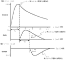
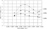
即ち、図6に照射電子ビームのエネルギ密度(J/cm2)と真空ハウジング1内希ガス(Ar)のガス圧(Torr)との関係を第3のパルス電源18による3つの異なる加速電圧の場合について示したように、ガス圧の変更によるエネルギ密度の変更設定が、比較的エネルギ密度の大きい領域で、加速電圧が高い場合ほど変更可能な幅が大きいことが判る。そして、このことから、逆に真空ハウジング1内のガス圧安定制御(<±1%)が重要なことが判る。 That is, FIG. 6 shows the relationship between the energy density (J / cm 2 ) of the irradiation electron beam and the gas pressure (Torr) of the rare gas (Ar) in the vacuum housing 1 at three different acceleration voltages by the third pulse power supply 18. As shown in the case, it can be seen that the change setting of the energy density by changing the gas pressure is a region where the energy density is relatively high, and the changeable range is larger as the acceleration voltage is higher. From this, on the contrary, it is understood that stable control of gas pressure in the vacuum housing 1 (<± 1%) is important.
なお、前述照射電子ビームのエネルギ密度の変更は、第3のパルス電源18による加速電圧の変更によっても可能であるが、この加速電圧はパルス幅が約1〜4μsと短くて変更等の自由度が小さく、かつ加速電圧の変更は、照射電子ビームのワーク材料内部へ侵入する深さを変化させて、ビームのエネルギを材料の表面層のみに与えて改質処理等をすると言う処理の目的を損なう可能性があるので、この第3のパルス電源18は、調整設定された一定条件で、繰り返し使用することが望ましい。 The energy density of the irradiation electron beam can be changed by changing the acceleration voltage by the third pulse power supply 18. However, the acceleration voltage has a short pulse width of about 1 to 4 μs, and the degree of freedom of change, etc. The change of the acceleration voltage is intended to modify the depth of penetration of the irradiated electron beam into the workpiece material and apply the energy of the beam only to the surface layer of the material for the modification process. The third pulse power supply 18 is desirably used repeatedly under a fixed condition that is set in an adjusted manner.
従来の電子ビーム蒸着は、前述したように、極めて細く絞ってエネルギ密度を所定に増大させた電子線を使用するものであるため、蒸着速度を大幅に増大させるとか、広い蒸着面積を持った基体の蒸着に適用するなどと言うことは、殆んど考えられたことが無かった。即ち、上記蒸着速度の増大や大面積の蒸着には、例えば、従来型の電子ビーム蒸着装置に於ける電子ビームハウジング部の断面積を拡大して、従来型電子ビーム発生銃を設置蒸発材料と共に、所望複数個並設すること等が考えられるが、これでは、極めて高価格となる丈でなく、大床面積を要する可能性などが考えられ、殆んど現実性がないことと思惟されるのである。 As described above, the conventional electron beam evaporation uses an electron beam with a very narrow aperture and a predetermined increase in energy density, so that the deposition rate is greatly increased, or a substrate having a wide evaporation area. It has hardly been considered to be applied to the deposition of the above. That is, for increasing the deposition rate and large-area deposition, for example, by expanding the cross-sectional area of the electron beam housing part in the conventional electron beam deposition apparatus, the conventional electron beam generating gun is installed together with the evaporation material. However, it may be possible to arrange a plurality of desired parallel arrangements, but this is not very expensive and may require a large floor area, which is considered to be almost unrealistic. It is.
然るに、蒸着の熱源としての電子ビームに、前述した金属、合金等の表面改質の処理加工に用いられる、被制御の低圧希ガス中で発生使用される照射軸方向と直角な方向の断面が、例えば、径が約60mm前後と極めて大きい電子ビームのパルスが、前記断面積が大きいことと、かつ、電子ビームがパルスである所から、そのパルスの照射時間の短縮化を計って、ビーム断面の各部に於けるエネルギ密度を蒸発材料の対応部の表層部分のもを瞬時に溶解、蒸発させ得るレベルに大きく為し得れば、純粋真空中の電子ビーム蒸着ではないものの、10−3Torr前後の可成りの希ガス残存真空中での、蒸着速度の速い、かつ蒸着領域が大きい面積の基体に対して適用できる電子ビーム蒸着方法及び装置が得られる可能性が生じるものである。 However, the electron beam as a heat source for vapor deposition has a cross section in a direction perpendicular to the irradiation axis direction used in the controlled low-pressure rare gas used in the surface modification processing of metals, alloys, and the like described above. For example, a pulse of an extremely large electron beam having a diameter of about 60 mm has a large cross section, and since the electron beam is a pulse, the irradiation time of the pulse is shortened, and the beam cross section If the energy density in each part of the material can be increased to a level at which the surface layer part of the corresponding part of the evaporation material can be instantaneously dissolved and evaporated, it is not an electron beam evaporation in a pure vacuum, but 10 −3 Torr. There is a possibility that an electron beam vapor deposition method and apparatus applicable to a substrate having a large vapor deposition area and a large vapor deposition area in a front and rear of a noble gas residual vacuum can be obtained.
そこで、本発明は、時間当たりの蒸発材の蒸発量を増大し、かつ、大きな蒸着面を有する基体の蒸着加工処理にも好適に適用できる電子ビーム蒸着方法及びその装置を開発したことにより提案される。 Therefore, the present invention has been proposed by developing an electron beam evaporation method and apparatus that can increase the evaporation amount of the evaporation material per hour and can be suitably applied to the evaporation processing of a substrate having a large evaporation surface. The
前述の本発明の目的は、(1)低圧ガス中の環状アノードと大面積カソード間の閉じ込め磁場中でアノードプラズマを有するグロー放電を発生させ、前記カソードに高い負の電圧パルスを印加することにより、前記プラズマを通路とする絞られない断面積の大きい電子ビームであって、該電子ビームの断面各部が、板状体に形成された蒸発材料の表面を照射することにより、薄い表層部分のみが瞬時に溶解して蒸発するエネルギ密度(1J/cm2以上)を持ち、かつ、前記表層部分以上に材料を溶解蒸発させない照射エネルギ量に制限するように照射時間を4μs以下の微小に制限された電子ビームのパルスを前記蒸発材料に休止時間を置いて繰り返し照射して溶解蒸発させ、該蒸発材料の前記照射表面と近接対向して配置した基体表面に被着させて蒸着膜を形成させる電子ビーム蒸着方法とすることにより達成される。 The objects of the present invention described above are as follows: (1) A glow discharge having an anode plasma is generated in a confined magnetic field between an annular anode in a low-pressure gas and a large area cathode, and a high negative voltage pulse is applied to the cathode. An electron beam having a large cross-sectional area that is not constricted with the plasma as a passage, and each section of the electron beam irradiates the surface of the evaporation material formed on the plate-like body, so that only a thin surface layer portion is obtained. It has an energy density (1 J / cm 2 or more) that dissolves and evaporates instantaneously, and the irradiation time is limited to a minute of 4 μs or less so as to limit the amount of irradiation energy that does not dissolve and evaporate the material beyond the surface layer portion. A pulse of an electron beam is repeatedly irradiated to the evaporating material with a pause time to dissolve and evaporate, and the substrate surface disposed in close proximity to the irradiated surface of the evaporating material is placed on the surface of the substrate. It is accomplished by an electron beam evaporation method for forming a deposited is allowed to deposited film.
また、前述の本発明の目的は、(2)前記基体が金型材の炭素鋼から成る金型で、蒸発材が金属チタンである前記(1)に記載の電子ビーム蒸着方法とすることにより達成される。 The object of the present invention is achieved by (2) the electron beam evaporation method according to (1), wherein the substrate is a mold made of carbon steel as a mold material, and the evaporation material is titanium metal. Is done.
また、前述の本発明の目的は、(3)電子ビーム発生部を収納する筒状のビームハウジング部と電子ビームの照射を受ける蒸発材料の設置部と該蒸発材料の電子ビーム照射面に近接して対向するように被蒸着基体を設置する取り付け部とを有する蒸着処理ハウジング部とを気密に結合し、所望の希ガスが所定の低圧状態に制御保持される真空ハウジング装置と、
前記ビームハウジング部内の蒸着処理ハウジング部側に設けられる環状乃至は筒状アノードと、該アノードの軸線上のアノードの他側に設けられ電子を放出する多数の針状突起を面状に並設して有する大面積のカソードと、前記カソードとアノード間に形成される電子加速空間に前記アノードの軸線の周りを該軸線と並行な磁力線で取り囲む磁場を形成するようにビームハウジング部外周に巻回しして設けたソレノイドと、
前記電子加速空間に前記磁場を所定時間形成するように前記ソレノイドを所望の電流値で励磁する第1のパルス電源と、
前記低圧希ガス空間中に設けられた前記カソードとアノード間に、前記第1のパルス電源によるソレノイドの励磁が所定の励磁状態になるのを待つか検出して電圧を印加し、電離によりアノードプラズマ及びカソードプラズマを形成させる第2のパルス電源と、
前記第2のパルス電源による電圧印加開始後の所望微小遅延時間後に、前記カソードに立ち上がり時間が短い負の高電圧を、電子ビーム照射時間となる所望の微小時間幅の間印加する第3のパルス電源とを備え、
前記蒸発材料の設置部は、板状体に形成された蒸発材料の蒸発面を、断面が面状の照射電子ビーム軸に対し所定角度傾斜させて配置され、前記基体が前記蒸発材料の蒸発面と垂直に相対向する方向の近接位置に電子ビームを遮蔽して設置され、該設置部が前記基体の取付位置及び姿勢の両方又は何れか一方の変更制御手段を有する電子ビーム蒸着装置とすることにより達成される。
The object of the present invention is as follows: (3) a cylindrical beam housing part that houses the electron beam generating part, an installation part for the evaporating material that receives the electron beam irradiation, and an electron beam irradiation surface of the evaporating material; And a vacuum housing device in which a desired noble gas is controlled and held in a predetermined low pressure state by airtightly coupling a vapor deposition processing housing portion having a mounting portion for installing a vapor deposition base so as to face each other,
An annular or cylindrical anode provided on the side of the vapor deposition processing housing in the beam housing and a large number of needle-like protrusions provided on the other side of the anode on the axis of the anode for emitting electrons are arranged side by side. A large-area cathode, and an electron acceleration space formed between the cathode and the anode, and wound around the beam housing portion so as to form a magnetic field surrounding the axis of the anode with magnetic lines of force parallel to the axis. A solenoid provided with
A first pulse power source for exciting the solenoid at a desired current value so as to form the magnetic field in the electron acceleration space for a predetermined time;
A voltage is applied between the cathode and the anode provided in the low-pressure noble gas space by detecting whether the excitation of the solenoid by the first pulse power supply is in a predetermined excitation state, and applying an ion to the anode plasma And a second pulse power source for forming a cathode plasma;
A third pulse that applies a negative high voltage with a short rise time to the cathode for a desired minute time width that becomes an electron beam irradiation time after a desired minute delay time after the start of voltage application by the second pulse power supply. With a power supply,
The evaporating material installation portion is disposed such that the evaporating surface of the evaporating material formed on the plate-like body is inclined at a predetermined angle with respect to the irradiation electron beam axis whose section is planar, and the base is the evaporating surface of the evaporating material An electron beam vapor deposition apparatus that is installed by shielding an electron beam at a close position in a direction perpendicular to each other, and the installation portion has a change control means for either or both of the attachment position and orientation of the substrate. Is achieved.
本発明によれば、10−4Torr程度、又はそれ以上のような充分高真空中の電子ビームではないももの、前記高真空に継ぐ、約10−3Torr程度の希ガスが僅かに残存する真空中を利用して得られる電子ビームであって、照射軸と直角な方向の断面を径が60mm程度以内と言う大面積であって、該電子ビームの断面の各部のエネルギ密度を、照射された蒸発材の表層部分が瞬時に溶解して、蒸発させ得る電子ビームとし得る一方で、前記蒸発材の電子ビームの照射した部分を、前記表層部分以上に材料を溶解、蒸発させない照射エネルギ量に制限するように照射時間を微小時間に制限した電子ビームのパルスとして、所定休止時間を置いて繰り返し照射し得るようにしたもので、従来例の電子ビーム蒸着に比較して格段に高速度の、又は時間当たりの蒸発量が大きい電子ビーム蒸着が行なえ、かつ、大きくて広い蒸着面を持つ基体に対しても電子ビーム蒸着が適用できるようになるのである。 According to the present invention, a rare gas of about 10 −3 Torr, which is not an electron beam in a sufficiently high vacuum, such as about 10 −4 Torr or higher, or about 10 −3 Torr is left behind. An electron beam obtained by utilizing a vacuum, and a cross section perpendicular to the irradiation axis is a large area whose diameter is within about 60 mm, and the energy density of each part of the cross section of the electron beam is irradiated. While the surface layer portion of the evaporated material can be instantly melted to be an electron beam that can be evaporated, the portion irradiated with the electron beam of the evaporated material has an irradiation energy amount that does not dissolve and evaporate the material more than the surface layer portion. As an electron beam pulse whose irradiation time is limited to a minute time so that it can be limited, it can be irradiated repeatedly with a predetermined pause time, which is much faster than conventional electron beam evaporation. Thus, electron beam evaporation with a large evaporation amount per hour can be performed, and electron beam evaporation can be applied to a substrate having a large and wide evaporation surface.
本発明において使用する断面が大きい大面積の電子ビームのパルスは、前述の如くして得られるものであって、各パルスの電子ビームは先ずそのエネルギ密度(J/cm2)が使用する蒸着剤の種類や材質により、電子ビームが照射された蒸発材の表面各部において、表層部分が瞬時(前記第3のパルス電源18による負の高電圧のパルスの時間幅、1−4μs以内)に溶解して蒸発を開始する以上のエネルギ密度のもの、通常好ましくは少なくとも約3J/cm2以上となるように調整設定される。 The large-area electron beam pulse used in the present invention is obtained as described above, and the electron beam of each pulse is first deposited by the energy density (J / cm 2 ). Depending on the type and material of the material, the surface layer of each part of the surface of the evaporation material irradiated with the electron beam dissolves instantaneously (within the time width of the negative high voltage pulse by the third pulse power supply 18 within 1 to 4 μs). The energy density is higher than that at which evaporation starts, and is preferably adjusted to be at least about 3 J / cm 2 or more.
次に、前述のようにエネルギ密度が調整、設定された電子ビームは、これを蒸発材に照射したとき、蒸発材の表面表層部分が、所定微小厚み以上に溶解、蒸発が進行しないように、即ち、照射エネルギ量を所定量以内に制限するために、電子ビームの照射を所定微小時間で停止し、所定照射休止時間の後、次回の電子ビームパルスの照射の工程に移行する如く、電子ビームの照射をパルス化し、以後パルス照射を必要回数繰り返すように為されるものである。 Next, when the electron beam whose energy density is adjusted and set as described above is irradiated onto the evaporation material, the surface surface layer portion of the evaporation material is dissolved to a predetermined minute thickness or more, and evaporation does not proceed. That is, in order to limit the irradiation energy amount within a predetermined amount, the electron beam irradiation is stopped for a predetermined minute time, and after the predetermined irradiation stop time, the electron beam pulse is transferred to the next irradiation step. The pulse irradiation is pulsed and the pulse irradiation is repeated as many times as necessary.
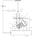
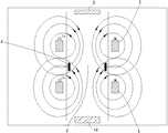
図1は、本発明の電子ビーム蒸着方法及び装置を説明するために真空ハウジング1内の蒸着加工処理ハウジング部1B内に設置される蒸着加工処理部1Cを中心に全体を模型的に示した側面図で、カソード8と環状アノード6の間に第3のパルス電源18から30KVの極めて短い(4μs以内)電圧パルスを印加して、大面積の電子ビーム11を発生させ前記蒸着加工処理部1Cに照射した態様を示している。 FIG. 1 is a side view schematically showing the whole of a deposition processing section 1C installed in a deposition processing housing section 1B in a vacuum housing 1 in order to explain an electron beam deposition method and apparatus of the present invention. In the figure, an extremely short (within 4 μs) voltage pulse of 30 KV is applied between the cathode 8 and the annular anode 6 to generate a large-area electron beam 11 to the vapor deposition processing unit 1C. The irradiation mode is shown.
図に於いて、23は蒸着加工処理ハウジング部1Bの底部付近に設けられる加工台で、通常前記アノード6と同電位に保持される加工台23上に蒸着加工処理部1Cが以下のように形成配置されている。即ち、前記ビームハウジング部1Aから照射される大面積電子ビーム11の部位には、板状に形成されたチタン、ニッケル、銅、鉄、タングステン、モリブデンや珪素等の金属、カーボン等の蒸発材料20の蒸発面を前記照射電子ビーム11の軸に対し所定角度傾斜させた状態で設置して保持する蒸発材設置台19が設けられ、この設置台19に設置された蒸発材20の蒸発面とほぼ垂直の方向の位置にあるように電子ビーム11から遮蔽して、蒸着基体21を取付け保持する基体取り付け治具22が設けられる。
In the figure,
そしてこの蒸着基体21の取り付け治具22の頂部、電子ビーム遮蔽の庇部22Aには、前記照射大面積電子ビーム11が各局部に於いて所定のエネルギ密度(J/cm2)以上で、全体的にほぼ均一である面のビームに整流するマスク板24が設けられ、また、取り付け基体21に対する図示紙面左右方向とこれと直交する表裏方向の微小距離の、真空キャンド型リニアモータ等の移動位置決め装置22Bと、前記基体21の蒸発材20蒸発面との対向面角度の微調整手段22Cとが設けられている。
Then, the irradiation large-area electron beam 11 is not less than a predetermined energy density (J / cm 2 ) at each local portion on the top of the
また、前記蒸発材20の設置台19には、鉄材又は銅合金材が使用され、図示していないが、必要に応じ前記蒸発材20を裏側から冷却する冷却手段が内設されりと共に、取り付けた蒸発材20の電子ビーム照射面を、ビーム照射軸又は基体21の蒸着面との垂直対向軸に対する傾斜角度を調整する角度調整装置19A、及び蒸発材20の表面蒸発面の大きさが照射電子ビーム11の照射面積よりも或る程度以上大きい場合、また、蒸発面領域を全体的に均一にしたい場合などに、設置台19を加工台23に対し、紙面上左右及び上下又は表裏方向に移動または揺動状で移動させる移動装置19Bが設けられている。
Further, the mounting
前記蒸発材20として金属チタン板を用い電子ビーム11の照射軸に対して約45°に傾斜させて設置し、之に対しSKD11などの金型材の炭素鋼からなる表面粗さ約4μmRmaxの金型を基体21として、その蒸着面を蒸発材20の蒸発面と並行で垂直に相対向させた状態として、電子ビーム11の径を約5.5mm、ビームの平均エネルギ密度を約4.5J/cm2、ビーム照射の制御パルス幅を約2μsとして、約7−8s間隔で繰り返し照射するようにした。 A metal titanium plate is used as the evaporating material 20 and is installed at an inclination of about 45 ° with respect to the irradiation axis of the electron beam 11, and a mold having a surface roughness of about 4 μm Rmax made of carbon steel as a mold material such as SKD11. Is the base 21 and the vapor deposition surface is vertically opposed to the evaporation surface of the evaporating material 20, and the diameter of the electron beam 11 is about 5.5 mm, and the average energy density of the beam is about 4.5 J / cm. 2. The control pulse width of beam irradiation was set to about 2 μs, and irradiation was repeatedly performed at intervals of about 7-8 s.
各電子ビームのパルス照射の毎に、蒸発材20の表層の約1μm厚以内の部分が溶解して蒸発を始めた所で電子ビーム11の継続照射が断たれ熱拡散冷却の段階に移行する間に蒸発状態に到ったチタンの原子、分子、イオン、または蒸気状微粒子乃至は細片状物の雲状物が蒸発面に対し直角に立ち登り、直前の位置にある基体21の表面にぶつかって被着し、その被着の繰り返しにより堆積し、表面粗さが約3μmHmax以内のほぼ白銀色に輝くチタンの蒸着被覆乃至は被膜が形成されることになる。
During each pulse irradiation of each electron beam, the continuous irradiation of the electron beam 11 is cut off when the portion of the surface layer of the evaporation material 20 within a thickness of about 1 μm is melted and starts to evaporate, and the process proceeds to the thermal diffusion cooling stage. Then, titanium atoms, molecules, ions, or vaporous fine particles or flakes that are in a vaporized state rise up at right angles to the evaporation surface and collide with the surface of the
この場合、基体21は、前述炭素鋼の場合に限らず他の鉄材、銅又は銅合金材の場合にも、加温乃至は加熱の必要はなかったが、蒸発材20と基体21の種類や材質組み合わせに依っては、加熱が必要となることも考えられる。そして上述の蒸着条件に於ける溶解、蒸発した雲状物の生成時の温度は、約1500℃前後又はそれよりも高いと思われるので、純金属以外の分解温度がこれよりも低い化合物や混合物等は蒸発又は蒸着材として不適であると考えられるが、それ以外の分解温度高い、例えば、一部のセラミックスなどの非金属などは、エネルギ密度や照射パルス幅時間等の調整は必要ながら、蒸発材又は蒸着材としての適用は可能と考えられる。之に対し、被蒸着の基体21としては広範囲のものへの適用が可能と思惟されるが、前記各種の鉄材や銅系合金の外、各種のセラミックスへの適用は勿論可能である。
In this case, the
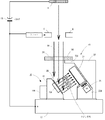
図2は、基体取付治具22の変更例を示すもので、基体21の対向角度調製手段22Cに替えて、前記基体21を蒸発材20の傾斜角度の面に平行な軸の廻りに回転及び/又は指令に応じ回転角度の位置決めをする回動制御装置25を前記移動位置決め装置22Bに搭載して設けることにより、基体21の回転方向外周面に対する蒸着を可能としたものである。
FIG. 2 shows a modified example of the
本発明の電子ビーム蒸着方法によれば、前述炭素鋼の金型に対するチタン被覆の表面処理の場合、その大面積電子ビームのパルスの繰り返し照射回数は、例えば、約30回程度のものであるから、蒸発材20や基体21等の設置調整、及び真空引き等の準備に或る程度時間を必要とするとしても、蒸着加工処理の段階に於いては、数10分以内の短時間での処理が行われるから、従来例の電子ビーム蒸着と対比すると、極めて高速化が計られるものである。
According to the electron beam evaporation method of the present invention, in the case of surface treatment of titanium coating on the carbon steel mold, the number of repeated irradiations of the large area electron beam pulse is, for example, about 30 times. Even if a certain amount of time is required for installation adjustment of the evaporating material 20 and the
なお、蒸発材20の種類にもよるが、蒸発材20又は設置台19と、蒸着基体21又は基体21背面に配置した電極板間に、通常後者をプラスとする電圧を印加して、蒸着加工処理を実行すると、電子ビーム11のパルスを蒸発材20表面に照射した時に立ち登る蒸気雲状物の吸引被着乃至は捕捉率が増大するが、蒸着加工処理速度に大きく影響する程のものではなかったが、蒸着加工処理ハウジング部1Bの内壁面や取り付け治具22表面などの汚染減には有効であった。
Although depending on the type of the evaporating material 20, a voltage that normally plus the latter is applied between the evaporating material 20 or the setting table 19 and the electrode plate disposed on the back surface of the evaporating
本発明は、電子ビーム蒸着を、蒸着面積の大きい蒸着基体への高速の蒸着手段として適用することができる。 The present invention can be applied to electron beam vapor deposition as a high-speed vapor deposition means for vapor deposition substrates having a large vapor deposition area.
1 真空ハウジング装置
2 スクロールポンプ
3 ターボ分子ポンプ
4 圧力調製弁
5 励磁ソレノイド
6 アノード
7 アノードプラズマ
8 カソード
9 カソードプラズマ
11 大面積の電子ビームパルス
13 回転台
14 コレクタ
15 ガスボンベ
16 第1のパルス電源
17 第2のパルス電源
18 第3のパルス電源
1A 筒状のビームハウジング部
1B 蒸着加工処理ハウジング部
1C 蒸着加工処理部
19 蒸発材設置台
19A 角度調製装置
19B 移動装置
20 蒸発材
21 蒸着基体
22 取り付け治具
22A 電子ビーム遮蔽庇
22B 移動位置決め装置
22C 角度微調整手段
23 加工台
24 マスク板
DESCRIPTION OF SYMBOLS 1
Claims (3)
前記ビームハウジング部内の蒸着処理ハウジング部側に設けられる環状乃至は筒状アノードと、該アノードの軸線上のアノードの他側に設けられ電子を放出する多数の針状突起を面状に並設して有する大面積のカソードと、前記カソードとアノード間に形成される電子加速空間に前記アノードの軸線の周りを該軸線と並行な磁力線で取り囲む磁場を形成するようにビームハウジング部外周に巻回しして設けたソレノイドと、
前記電子加速空間に前記磁場を所定時間形成するように前記ソレノイドを所望の電流値で励磁する第1のパルス電源と、
前記低圧希ガス空間中に設けられた前記カソードとアノード間に、前記第1のパルス電源によるソレノイドの励磁が所定の励磁状態になるのを待つか検出して電圧を印加し、電離によりアノードプラズマ及びカソードプラズマを形成させる第2のパルス電源と、
前記第2のパルス電源による電圧印加開始後の所望微小遅延時間後に、前記カソードに立ち上がり時間が短い負の高電圧を、電子ビーム照射時間となる所望の微小時間幅の間印加する第3のパルス電源とを備え、
前記蒸発材料の設置部は、板状体に形成された蒸発材料の蒸発面を、断面が面状の照射電子ビーム軸に対し所定角度傾斜させて配置され、前記基体が前記蒸発材料の蒸発面と垂直に相対向する方向の近接位置に電子ビームを遮蔽して設置され、該設置部が前記基体の取付位置及び姿勢の両方又は何れか一方の変更制御手段を有することを特徴とする電子ビーム蒸着装置。
A cylindrical beam housing portion that houses the electron beam generating portion, an installation portion for the evaporating material that is irradiated with the electron beam, and an attachment portion that installs the substrate to be deposited so as to face the electron beam irradiation surface of the evaporating material in close proximity to each other And a vacuum housing device in which a desired rare gas is controlled and held in a predetermined low pressure state.
An annular or cylindrical anode provided on the side of the vapor deposition processing housing in the beam housing and a large number of needle-like protrusions provided on the other side of the anode on the axis of the anode for emitting electrons are arranged side by side. A large-area cathode, and an electron acceleration space formed between the cathode and the anode, and wound around the beam housing portion so as to form a magnetic field surrounding the axis of the anode with magnetic lines of force parallel to the axis. A solenoid provided with
A first pulse power source for exciting the solenoid at a desired current value so as to form the magnetic field in the electron acceleration space for a predetermined time;
A voltage is applied between the cathode and the anode provided in the low-pressure noble gas space by detecting whether the excitation of the solenoid by the first pulse power supply is in a predetermined excitation state, and applying an ion to the anode plasma And a second pulse power source for forming a cathode plasma;
A third pulse that applies a negative high voltage with a short rise time to the cathode for a desired minute time width that becomes an electron beam irradiation time after a desired minute delay time after the start of voltage application by the second pulse power supply. With a power supply,
The evaporating material installation portion is disposed such that the evaporating surface of the evaporating material formed on the plate-like body is inclined at a predetermined angle with respect to the irradiation electron beam axis whose section is planar, and the base is the evaporating surface of the evaporating material The electron beam is installed by shielding the electron beam at a position close to the direction perpendicular to the substrate, and the installation portion has change control means for either or both of the attachment position and the posture of the base body. Vapor deposition equipment.
Priority Applications (1)
| Application Number | Priority Date | Filing Date | Title |
|---|---|---|---|
| JP2004109932A JP2005290510A (en) | 2004-04-02 | 2004-04-02 | Electron beam vapor deposition method and apparatus therefor |
Applications Claiming Priority (1)
| Application Number | Priority Date | Filing Date | Title |
|---|---|---|---|
| JP2004109932A JP2005290510A (en) | 2004-04-02 | 2004-04-02 | Electron beam vapor deposition method and apparatus therefor |
Publications (1)
| Publication Number | Publication Date |
|---|---|
| JP2005290510A true JP2005290510A (en) | 2005-10-20 |
Family
ID=35323775
Family Applications (1)
| Application Number | Title | Priority Date | Filing Date |
|---|---|---|---|
| JP2004109932A Pending JP2005290510A (en) | 2004-04-02 | 2004-04-02 | Electron beam vapor deposition method and apparatus therefor |
Country Status (1)
| Country | Link |
|---|---|
| JP (1) | JP2005290510A (en) |
Cited By (5)
| Publication number | Priority date | Publication date | Assignee | Title |
|---|---|---|---|---|
| WO2010057721A1 (en) * | 2008-11-21 | 2010-05-27 | Cameca | Tomography atomic probe comprising a high voltage electric pulse electro-optical generator |
| JP2010267950A (en) * | 2008-11-06 | 2010-11-25 | Panasonic Corp | Nitride-based semiconductor device and manufacturing method thereof |
| KR20190074760A (en) * | 2017-12-20 | 2019-06-28 | 한국세라믹기술원 | A vacuum deposition apparatus using a plurality of target structures |
| CN114959593A (en) * | 2022-05-30 | 2022-08-30 | 咸阳旭光晶圆材料科技有限公司 | Laser crystal coating device and coating method thereof |
| CN117506177A (en) * | 2023-11-09 | 2024-02-06 | 清华大学 | Vortex laser processing vector light field particle gradient force field controlled extraction device and method |
-
2004
- 2004-04-02 JP JP2004109932A patent/JP2005290510A/en active Pending
Cited By (9)
| Publication number | Priority date | Publication date | Assignee | Title |
|---|---|---|---|---|
| JP2010267950A (en) * | 2008-11-06 | 2010-11-25 | Panasonic Corp | Nitride-based semiconductor device and manufacturing method thereof |
| WO2010057721A1 (en) * | 2008-11-21 | 2010-05-27 | Cameca | Tomography atomic probe comprising a high voltage electric pulse electro-optical generator |
| FR2938963A1 (en) * | 2008-11-21 | 2010-05-28 | Cameca | TOMOGRAPHIC ATOMIC PROBE COMPRISING AN ELECTRO-OPTICAL GENERATOR OF HIGH VOLTAGE ELECTRIC PULSES |
| US8276210B2 (en) | 2008-11-21 | 2012-09-25 | Cameca | Tomographic atom probe comprising an electro-optical generator of high-voltage electrical pulses |
| KR20190074760A (en) * | 2017-12-20 | 2019-06-28 | 한국세라믹기술원 | A vacuum deposition apparatus using a plurality of target structures |
| KR102005555B1 (en) | 2017-12-20 | 2019-07-30 | 한국세라믹기술원 | A vacuum deposition apparatus using a plurality of target structures |
| CN114959593A (en) * | 2022-05-30 | 2022-08-30 | 咸阳旭光晶圆材料科技有限公司 | Laser crystal coating device and coating method thereof |
| CN114959593B (en) * | 2022-05-30 | 2023-09-19 | 咸阳旭光晶圆材料科技有限公司 | Laser crystal coating device and coating method thereof |
| CN117506177A (en) * | 2023-11-09 | 2024-02-06 | 清华大学 | Vortex laser processing vector light field particle gradient force field controlled extraction device and method |
Similar Documents
| Publication | Publication Date | Title |
|---|---|---|
| US9771648B2 (en) | Method of ionized physical vapor deposition sputter coating high aspect-ratio structures | |
| CA2411174C (en) | A process and apparatus for plasma activated deposition in a vacuum | |
| JP4722486B2 (en) | High deposition rate sputtering | |
| USRE37537E1 (en) | Method and apparatus for altering material | |
| US8568572B2 (en) | Very low pressure high power impulse triggered magnetron sputtering | |
| EP2602354A1 (en) | Filtered cathodic vacuum arc deposition apparatus and method | |
| EP0511153A1 (en) | Plasma enhancement apparatus and method for physical vapor deposition | |
| JP6101238B2 (en) | Coating apparatus for coating a substrate and method for coating a substrate | |
| RU2012111218A (en) | ION-PLASMA ELECTRON RADIATORS FOR Smelting Furnace | |
| US7557511B2 (en) | Apparatus and method utilizing high power density electron beam for generating pulsed stream of ablation plasma | |
| CA3203247A1 (en) | Additive manufacturing using powder bed fusion | |
| JP3481953B2 (en) | Equipment for coating substrates | |
| JP2005290510A (en) | Electron beam vapor deposition method and apparatus therefor | |
| US20070256927A1 (en) | Coating Apparatus for the Coating of a Substrate and also Method for Coating | |
| JP2005076061A (en) | Method and device for reforming surface of metal member | |
| Ryabchikov et al. | Features of the formation of ultralow energy high-intensity metal and gaseous ion beams | |
| JP2008280579A (en) | Electron-beam sputtering device | |
| Perry et al. | An overview of some advanced surface technology in Russia | |
| JPH11224797A (en) | Plasma generator and thin film forming apparatus | |
| KR102809722B1 (en) | pure metal ion implantation apparatus using electron beam ion source capable of extracting single metal Ion Beam | |
| RU2607398C2 (en) | Method of coatings application by plasma spraying and device for its implementation | |
| JP3330159B2 (en) | Dynamic mixing device | |
| RU2619543C1 (en) | Pulse electron-beam metal product surface polishing method | |
| KR102858038B1 (en) | Composite ion implantation apparatus and RCS reduction method for weapon system materials using composite ion source | |
| JP2014034698A (en) | Film deposition method and apparatus |