JP2005259972A - Surface-mounting led - Google Patents
Surface-mounting led Download PDFInfo
- Publication number
- JP2005259972A JP2005259972A JP2004069311A JP2004069311A JP2005259972A JP 2005259972 A JP2005259972 A JP 2005259972A JP 2004069311 A JP2004069311 A JP 2004069311A JP 2004069311 A JP2004069311 A JP 2004069311A JP 2005259972 A JP2005259972 A JP 2005259972A
- Authority
- JP
- Japan
- Prior art keywords
- frame
- transparent resin
- led
- shaped member
- led chip
- Prior art date
- Legal status (The legal status is an assumption and is not a legal conclusion. Google has not performed a legal analysis and makes no representation as to the accuracy of the status listed.)
- Pending
Links
Images

Classifications
-
- H—ELECTRICITY
- H01—ELECTRIC ELEMENTS
- H01L—SEMICONDUCTOR DEVICES NOT COVERED BY CLASS H10
- H01L2224/00—Indexing scheme for arrangements for connecting or disconnecting semiconductor or solid-state bodies and methods related thereto as covered by H01L24/00
- H01L2224/01—Means for bonding being attached to, or being formed on, the surface to be connected, e.g. chip-to-package, die-attach, "first-level" interconnects; Manufacturing methods related thereto
- H01L2224/42—Wire connectors; Manufacturing methods related thereto
- H01L2224/47—Structure, shape, material or disposition of the wire connectors after the connecting process
- H01L2224/48—Structure, shape, material or disposition of the wire connectors after the connecting process of an individual wire connector
- H01L2224/4805—Shape
- H01L2224/4809—Loop shape
- H01L2224/48091—Arched
-
- H—ELECTRICITY
- H01—ELECTRIC ELEMENTS
- H01L—SEMICONDUCTOR DEVICES NOT COVERED BY CLASS H10
- H01L2224/00—Indexing scheme for arrangements for connecting or disconnecting semiconductor or solid-state bodies and methods related thereto as covered by H01L24/00
- H01L2224/01—Means for bonding being attached to, or being formed on, the surface to be connected, e.g. chip-to-package, die-attach, "first-level" interconnects; Manufacturing methods related thereto
- H01L2224/42—Wire connectors; Manufacturing methods related thereto
- H01L2224/47—Structure, shape, material or disposition of the wire connectors after the connecting process
- H01L2224/48—Structure, shape, material or disposition of the wire connectors after the connecting process of an individual wire connector
- H01L2224/484—Connecting portions
- H01L2224/48463—Connecting portions the connecting portion on the bonding area of the semiconductor or solid-state body being a ball bond
- H01L2224/48465—Connecting portions the connecting portion on the bonding area of the semiconductor or solid-state body being a ball bond the other connecting portion not on the bonding area being a wedge bond, i.e. ball-to-wedge, regular stitch
-
- H—ELECTRICITY
- H01—ELECTRIC ELEMENTS
- H01L—SEMICONDUCTOR DEVICES NOT COVERED BY CLASS H10
- H01L2224/00—Indexing scheme for arrangements for connecting or disconnecting semiconductor or solid-state bodies and methods related thereto as covered by H01L24/00
- H01L2224/73—Means for bonding being of different types provided for in two or more of groups H01L2224/10, H01L2224/18, H01L2224/26, H01L2224/34, H01L2224/42, H01L2224/50, H01L2224/63, H01L2224/71
- H01L2224/732—Location after the connecting process
- H01L2224/73251—Location after the connecting process on different surfaces
- H01L2224/73265—Layer and wire connectors
Abstract
Description
本発明は、LEDチップからの光を蛍光体層を介して出射させて、LEDチップからの光と蛍光体層からの蛍光とを混色させて、外部に出射するようにした表面実装型LEDに関するものである。 The present invention relates to a surface-mounted LED in which light from an LED chip is emitted through a phosphor layer, and the light from the LED chip and fluorescence from the phosphor layer are mixed and emitted to the outside. Is.
従来、白色LEDとして、青色LEDチップからの光を蛍光体層で黄色光に変換して、青色LEDチップからの青色光と混色することにより、外部に白色光を出射するようにした白色LEDが知られている。
このような白色LEDは、例えば図4に示すように構成されている。
即ち、図4において、白色LED1は、一対のリードフレーム2,3と、これらのリードフレーム2,3を所定位置に保持するように一体成形された枠状部材4と、この枠状部材4の凹陥部4a内に露出する一方のリードフレーム2のチップ実装部2a上に実装された青色LEDチップ5と、上記枠状部材4の凹陥部4a内にて青色LEDチップ5を包囲するように充填された蛍光体を混入した透明樹脂部6と、から構成されている。
Conventionally, as a white LED, a white LED that emits white light to the outside by converting light from a blue LED chip into yellow light by a phosphor layer and mixing it with blue light from a blue LED chip is used. Are known.
Such a white LED is configured, for example, as shown in FIG.
That is, in FIG. 4, the
上記リードフレーム2,3は、それぞれその先端にチップ実装部2a及びボンディング部3aを備えるように、銅等の導電性材料から形成されていると共に、他端が、枠状部材4の側面から下面に回り込んで、表面実装のための接続部2b,3bを構成している。
The
上記枠状部材4は、上記リードフレーム2,3に対してインサート成形等により一体に形成されており、上面中央に、すり鉢状に上方に向かって拡る凹陥部4aを備えている。
ここで、上記凹陥部4aの底部にて、上記リードフレーム2,3の先端2a,3aが露出するようになっている。
また、上記枠状部材4は、反射率を考慮し、一般にナイロン系熱可塑性樹脂、例えばガラスフィラーと酸化チタンを添加した白色のポリフタルアミド(PPA)樹脂が使用される。
The frame-
Here, the tips 2a and 3a of the
The frame-
上記LEDチップ5は、上記枠状部材4の凹陥部4a内にて、一方のリードフレーム2の先端のチップ実装部2a上に接合されると共に、その上面に設けられた電極が、隣接する他方のリードフレーム3の先端のボンディング部3aに対してボンディングワイヤ7により電気的に接続されるようになっている。
The
ここで、上記青色LEDチップ5は、例えば主として窒化物系半導体材料から構成されており、上記リードフレーム2,3を介して駆動電圧が印加されたとき、420乃至480nmにピーク波長を有する光を発するようになっている。
Here, the
上記透明樹脂部6は、微粒子状の蛍光体6aを混入した例えば透明エポキシ樹脂等から構成されており、上記枠状部材4の凹陥部4a内に充填され、硬化されている。
そして、この透明樹脂部6に、青色LEDチップ5からの青色光が入射することにより、蛍光体6aが励起され、蛍光体6aから黄色光を発生させると共に、これらの混色による白色光が外部に出射するようになっている。
The
Then, when the blue light from the
ここで、蛍光体6aは、例えばセリウム,ガドリニウム等をドープしたYAG蛍光体や、このようなYAG蛍光体にてイットリウムを他の元素に置換したもの、あるいはオルトシリケート誘導体等が使用され、530乃至590nmにピーク波長を有する蛍光を発するようになっている。 Here, as the phosphor 6a, for example, a YAG phosphor doped with cerium, gadolinium, or the like, a yttrium substituted with such a YAG phosphor, or an orthosilicate derivative is used. It emits fluorescence having a peak wavelength at 590 nm.
このような構成の白色LED1によれば、一対のリードフレーム2,3を介して青色LEDチップ5に駆動電圧が印加されると、青色LEDチップ5が発光し、この光が透明樹脂部6に混入された蛍光体6aに入射することにより、蛍光体6aが励起されて黄色光を発生させる。
そして、白色LED1は、この黄色光を、青色LEDチップ5からの青色光と混色させることにより、白色光として、直接に、あるいは枠状部材4の凹陥部4aの側面で反射して、外部に出射させることになる。
According to the
The
ところで、このような構成の白色LED1においては、以下のような問題がある。
即ち、封止樹脂である凹陥部4aに充填される透明樹脂部6を構成するエポキシ樹脂が、枠状部材4を構成するPPA樹脂と熱膨張係数が異なることから、使用に伴って、その界面に剥離が生ずることになる。このため、青色LEDチップ5からの青色光または透明樹脂部6からの黄色光あるいは混色による白色光が枠状部材4の凹陥部4aの内面との境界領域に進んだ場合、透明樹脂部6と枠状部材4との間に間隙が生ずることから、この境界面による反射効率が著しく低下しすることになり、白色LED1における白色光の取出し効率が低下するので、信頼性が損なわれてしまう。
Incidentally, the
That is, since the epoxy resin constituting the
また、青色LEDチップ5とリードフレーム2のチップ実装部2aを良好に接合するためには、Au−Sn共晶接合という方法があるが、枠状部材4を構成するPPA樹脂の耐熱性が280℃程度までであることから、共晶接合を行なうために必要な300℃程度の温度に対する耐熱性を得ることができなかった。
Further, in order to satisfactorily bond the
このような問題は、青色LEDチップだけでなく、他の色を発光するLEDチップからの光と蛍光体の励起光の混色光である他の色の光を出射するLEDにおいても、またリードフレームの代わりにチップ基板を使用したLEDにおいても、同様に存在する。 Such a problem occurs not only in a blue LED chip, but also in an LED that emits light of another color, which is a mixed color light of an LED chip that emits another color and excitation light of a phosphor, and a lead frame. This also exists in the LED using a chip substrate instead of.
本発明は、以上の点から、簡単な構成により、枠状部材と透明樹脂部を構成する封止樹脂との間の剥離を防止すると共に、LEDチップの共晶接合が行なわれ得るようにした、表面実装型LEDを提供することを目的としている。 From the above points, the present invention prevents the peeling between the frame-shaped member and the sealing resin constituting the transparent resin portion with a simple configuration, and allows eutectic bonding of the LED chip to be performed. The object is to provide a surface-mounted LED.
上記目的は、本発明によれば、LEDチップを収容すべき凹陥部を備えた枠状部材と、この枠状部材の凹陥部の底部に露出するチップ実装部及びボンディング部を有し且つ上記枠状部材の下面に回り込む一対のリードフレームと、上記枠状部材の凹陥部内にて上記チップ実装部上に接合され且つその表面が上記ボンディング部に対して接続されるLEDチップと、上記枠状部材の凹陥部内に充填される透明樹脂部と、を含んでいる表面実装型LEDであって、上記枠状部材が、主として透明樹脂部を構成する高耐熱の熱硬化性透明樹脂から構成されており、上記LEDチップが、上記チップ実装部の表面に対して共晶接合されていることを特徴とする、表面実装型LEDにより、達成される。 According to the present invention, the above object has a frame-like member having a recessed portion that should accommodate an LED chip, a chip mounting portion and a bonding portion that are exposed at the bottom of the recessed portion of the frame-like member, and the frame. A pair of lead frames that wrap around the lower surface of the shaped member; an LED chip that is joined to the chip mounting portion in the recessed portion of the frame-like member and whose surface is connected to the bonding portion; and the frame-like member A surface-mount type LED including a transparent resin portion filled in the recessed portion, wherein the frame-shaped member is mainly composed of a high heat-resistant thermosetting transparent resin constituting the transparent resin portion. This is achieved by a surface-mounted LED, wherein the LED chip is eutectic bonded to the surface of the chip mounting portion.
本発明による表面実装型LEDは、好ましくは、上記枠状部材が、熱硬化性透明樹脂に酸化チタン及び/またはガラスフィラーを添加した材料から構成されている。 In the surface-mounted LED according to the present invention, preferably, the frame member is made of a material obtained by adding titanium oxide and / or glass filler to a thermosetting transparent resin.
本発明による表面実装型LEDは、好ましくは、上記枠状部材を構成する材料が、さらに酸化防止剤を添加されている。 In the surface-mount type LED according to the present invention, preferably, the material constituting the frame-like member is further added with an antioxidant.
本発明による表面実装型LEDは、好ましくは、上記透明樹脂部が、蛍光体を混入した透明樹脂により構成されており、上記LEDチップからの出射光により蛍光体を励起させて、出射光と励起光との混色光を外部に出射する。 In the surface-mount type LED according to the present invention, preferably, the transparent resin portion is made of a transparent resin mixed with a phosphor, and the phosphor is excited by the emitted light from the LED chip to be excited with the emitted light. Light of mixed color with light is emitted to the outside.
本発明による表面実装型LEDは、好ましくは、上記LEDチップが、青色LEDチップである。 In the surface mount type LED according to the present invention, preferably, the LED chip is a blue LED chip.
本発明による表面実装型LEDは、好ましくは、上記枠状部材が、上記一対のリードフレームに対してインサート成形により一体に構成されている。 In the surface-mounted LED according to the present invention, preferably, the frame-shaped member is integrally formed with the pair of lead frames by insert molding.
上記構成によれば、LEDチップに駆動電流が流れることにより、LEDチップから光が出射する。そして、LEDチップから出射した光は、透明樹脂部を介して直接に、あるいは枠状部材の凹陥部の内壁面で反射されて、外部に出射する。 According to the above configuration, light is emitted from the LED chip when a drive current flows through the LED chip. And the light radiate | emitted from LED chip is reflected by the inner wall surface of the recessed part of a frame-shaped member directly via a transparent resin part, and is radiate | emitted outside.
この場合、枠状部材が、その凹陥部内に充填される封止樹脂である透明樹脂部を構成する材料と同じ材料を主として使用して、例えばインサート成形によりリードフレームに対して一体に形成されている。従って、これらの枠状部材と透明樹脂部の熱膨張係数がほぼ同じであることから、枠状部材及び透明樹脂部がLEDチップの駆動により発生する熱によって温度変化しても、枠状部材と透明樹脂部が互いに剥離してしまうようなことがなく、信頼性が確保され得ることになる。 In this case, the frame-shaped member is formed integrally with the lead frame, for example, by insert molding, mainly using the same material as the material constituting the transparent resin portion which is the sealing resin filled in the recessed portion. Yes. Accordingly, since the thermal expansion coefficients of these frame-shaped members and the transparent resin portion are almost the same, even if the temperature of the frame-shaped member and the transparent resin portion is changed by the heat generated by driving the LED chip, The transparent resin parts do not peel from each other, and reliability can be ensured.
また、枠状部材が主として高耐熱の熱硬化性透明樹脂から構成されているので、枠状部材が耐熱性を有していることから、一方のリードフレームのチップ実装部に対してLEDチップを実装する際に、例えばAu−Sn共晶等の共晶接合を行なったとしても、共晶接合を行なうために必要な温度(例えば300℃)において上記枠状部材が影響を受けるようなことがなく、確実に共晶接合を行なうことが可能である。 In addition, since the frame-shaped member is mainly composed of a highly heat-resistant thermosetting transparent resin, the frame-shaped member has heat resistance. Therefore, the LED chip is attached to the chip mounting portion of one lead frame. When mounting, even if eutectic bonding such as Au-Sn eutectic is performed, the frame-shaped member may be affected at a temperature (for example, 300 ° C.) necessary for eutectic bonding. Thus, eutectic bonding can be reliably performed.
上記枠状部材が、熱硬化性透明樹脂に酸化チタン及び/またはガラスフィラーを添加した材料から構成されている場合には、熱硬化性透明樹脂を使用して、枠状部材に適した反射率を有する例えば白色の材料を得ることができる。 When the frame-shaped member is made of a material in which titanium oxide and / or glass filler is added to a thermosetting transparent resin, the reflectance suitable for the frame-shaped member is obtained using the thermosetting transparent resin. For example, a white material can be obtained.
上記枠状部材を構成する材料が、さらに酸化防止剤を添加されている場合には、この酸化防止剤によって経時変化による樹脂変色が防止されることになり、樹脂変色による反射率の低下が抑制され得ることになる。 When the material constituting the frame-like member is further added with an antioxidant, this antioxidant prevents resin discoloration due to aging, and suppresses a decrease in reflectance due to resin discoloration. Will be able to.
上記透明樹脂部が、蛍光体を混入した透明樹脂により構成されており、上記LEDチップからの出射光により蛍光体を励起させて、出射光と励起光との混色光を外部に出射する場合には、LEDチップからの出射光と透明樹脂部に混入された蛍光体の励起光との混色光、例えば白色光を外部に出射させることができる。 When the transparent resin portion is made of a transparent resin mixed with a phosphor, and the phosphor is excited by the light emitted from the LED chip and the mixed light of the emitted light and the excitation light is emitted to the outside. Can emit mixed color light of the emitted light from the LED chip and the excitation light of the phosphor mixed in the transparent resin portion, for example, white light to the outside.
上記LEDチップが、青色LEDチップである場合には、LEDチップからの青色光と透明樹脂部に混入された蛍光体の励起光、例えば黄色光との混色光、例えば白色光を外部に出射させることができる。 When the LED chip is a blue LED chip, the mixed light of the blue light from the LED chip and the excitation light of the phosphor mixed in the transparent resin part, for example, yellow light, for example, white light is emitted to the outside. be able to.
このようにして、本発明によれば、枠状部材を構成する材料が主として透明樹脂部と同じ材料から構成されていることにより、互いにほぼ同じ熱膨張係数を有しているので、温度変化によって枠状部材と透明樹脂部とが互いに剥離してしまうようなことがない。従って、信頼性の高い表面実装型LEDが得られることになる。
また、枠状部材が高耐熱材料から構成されていることにより、枠状部材の凹陥部内に露出している一方のリードフレームのチップ実装部にLEDチップを実装する際に、例えばAu−Sn共晶等の共晶接合を行なったとしても、枠状部材が共晶接合に必要な例えば300℃程度の温度で耐熱性を有しているので、枠状部材に影響を与えることなく、共晶接合を確実に行なうことができる。
Thus, according to the present invention, the material constituting the frame-shaped member is mainly composed of the same material as that of the transparent resin portion, and thus has substantially the same thermal expansion coefficient. The frame-shaped member and the transparent resin portion do not peel off from each other. Therefore, a highly reliable surface mount type LED can be obtained.
In addition, since the frame-shaped member is made of a high heat-resistant material, when mounting the LED chip on the chip mounting portion of one lead frame exposed in the recessed portion of the frame-shaped member, for example, Au-Sn Even if eutectic bonding such as crystal is performed, the frame-shaped member has heat resistance at a temperature of, for example, about 300 ° C. necessary for eutectic bonding, so that the eutectic is not affected without affecting the frame-shaped member. Bonding can be performed reliably.
以下、この発明の好適な実施形態を図1を参照しながら、詳細に説明する。
尚、以下に述べる実施形態は、本発明の好適な具体例であるから、技術的に好ましい種々の限定が付されているが、本発明の範囲は、以下の説明において特に本発明を限定する旨の記載がない限り、これらの態様に限られるものではない。
Hereinafter, a preferred embodiment of the present invention will be described in detail with reference to FIG.
The embodiments described below are preferable specific examples of the present invention, and thus various technically preferable limitations are given. However, the scope of the present invention particularly limits the present invention in the following description. As long as there is no description of the effect, it is not restricted to these aspects.
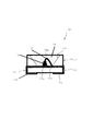
図1は、本発明による表面実装型白色LEDの一実施形態の構成を示している。
図1において、表面実装型白色LED10は、一対のリードフレーム11,12と、これらのリードフレーム11,12を所定位置に保持するように一体成形された枠状部材13と、この枠状部材13の凹陥部13a内に露出する一方のリードフレーム11のチップ実装部11a上に実装された青色LEDチップ14と、上記枠状部材13の凹陥部13a内にて青色LEDチップ14を包囲するように充填された蛍光体を混入した透明樹脂部15と、から構成されている。
FIG. 1 shows the configuration of an embodiment of a surface-mounted white LED according to the present invention.
In FIG. 1, the surface-mount
上記リードフレーム11及び12は、それぞれその上記凹陥部13a内に露出する先端にチップ実装部11a及びボンディング部12aを備えるように、アルミニウム等の導電性材料から形成されていると共に、他端が、枠状部材13の側面から下面に回り込んで、表面実装のための接続部11b及び12bを構成している。
Each of the lead frames 11 and 12 is formed of a conductive material such as aluminum so that the tip mounting portion 11a and the bonding portion 12a are provided at the tip exposed in the recessed portion 13a. Connecting
上記枠状部材13は、上記リードフレーム11,12に対してインサート成形により一体に形成されており、上面中央に、すり鉢状に上方に向かって拡る凹陥部13aを備えている。
ここで、上記凹陥部13aの底部にて、上記リードフレーム11,12の先端のチップ実装部11a及びボンディング部12aが露出するようになっている。
The frame-shaped
Here, the chip mounting portion 11a and the bonding portion 12a at the tips of the lead frames 11 and 12 are exposed at the bottom of the recessed portion 13a.
また、上記枠状部材13は、本発明に基づいて、主として後述する透明樹脂部15を構成する材料、即ち高耐熱の熱硬化性透明樹脂、例えば透明エポキシ樹脂から構成され、さらに例えばガラスフィラーと酸化チタンを添加されると共に、酸化防止剤を添加されている。
ここで、上記ガラスフィラー及び酸化チタンは、枠状部材13の反射率を向上させるためのものであり、また酸化防止剤は、熱硬化性透明樹脂の酸化による樹脂変色を防止し、反射率の低下を抑制するものである。
The frame-shaped
Here, the glass filler and titanium oxide are for improving the reflectance of the frame-
上記枠状部材13は、前述したリードフレーム11,12に対してインサート成形されるが、その際、例えば主たる構成材料である透明エポキシ材料に関して、所謂Bステージ状態で反応を停止させて、粉末状に粉砕したものを押し固めたタブレットを形成した後、このタブレットを使用して所謂トランスファーモールドにより成形される。
The frame-
上記LEDチップ5は、上記枠状部材13の凹陥部13a内にて、一方のリードフレーム13の先端のチップ実装部13a上に接合されると共に、その表面に設けられた電極が、隣接して凹陥部13a内に露出する他方のリードフレーム12の先端のボンディング部12aに対してボンディングワイヤ16により電気的に接続されるようになっている。
The
ここで、上記LEDチップ14は、所謂青色LEDチップであって、例えば主として窒化物系半導体材料から構成されており、駆動電圧が印加されたとき、420乃至480nmにピーク波長を有する光を発するようになっている。
Here, the
さらに、上記LEDチップ14は、上記チップ実装部11aに対して、例えばAu−Sn共晶等の共晶接合によって接合されるようになっている。その際、枠状部材13が前述したように主として高耐熱の熱硬化性透明樹脂から構成されていることにより、共晶接合に必要な温度(例えば300℃)において耐熱性を有しているので、枠状部材13に影響を与えることなく、LEDチップ14のチップ実装部11aに対する共晶接合が行なわれ得る。
Further, the
上記透明樹脂部15は、微粒子状の蛍光体15aを混入した高耐熱の熱硬化性透明樹脂、例えば透明エポキシ樹脂等から構成されており、上記枠状部材13の凹陥部13a内に充填され、硬化されている。
そして、この透明樹脂部15に、LEDチップ14からの青色光が入射することにより、蛍光体15aが励起され、蛍光体15aから黄色光を発生させると共に、これらの混色による白色光が外部に出射するようになっている。
The
When the blue light from the
ここで、蛍光体15aは、例えばセリウム,ガドリニウム等をドープしたYAG蛍光体や、このようなYAG蛍光体にてイットリウムを他の元素に置換したもの、あるいはオルトシリケート誘導体等が使用され、530乃至590nmにピーク波長を有する蛍光を発するようになっている。 Here, as the phosphor 15a, for example, a YAG phosphor doped with cerium, gadolinium or the like, a yttrium substituted with such a YAG phosphor, or an orthosilicate derivative is used. It emits fluorescence having a peak wavelength at 590 nm.
本発明実施形態による表面実装型白色LED10は、以上のように構成されており、製造の際には、以下のようにして製造される。
即ち、まず、リードフレーム11,12に対して枠状部材13がインサート成形される。
その後、枠状部材13の凹陥部13a内にて、リードフレーム11のチップ実装部11a上にLEDチップ14が共晶接合によって接合されると共に、リードフレーム12のボンディング部12aに対してワイヤボンディングされる。
次に、枠状部材13の凹陥部13a内に、蛍光体15aを混入した高耐熱の熱硬化性透明樹脂が充填され、硬化されることにより、透明樹脂部15が形成され、表面実装型LED10が完成する。
The surface-mounted
That is, first, the frame-shaped
Thereafter, the
Next, the recessed portion 13a of the frame-shaped
このような構成の表面実装型LED10によれば、一対のリードフレーム11,12を介してLEDチップ14に駆動電圧が印加されると、LEDチップ14が発光して、青色光が出射する。
そして、LEDチップ14から出射する青色光の一部が、透明樹脂部15に混入された蛍光体15aに入射することにより、蛍光体15aが励起されて、黄色光を発生させる。
この黄色光が、LEDチップ14からの青色光と混色されることにより、白色光となって、透明樹脂部15を通って、透明樹脂部15の上面から外部に出射することになる。
According to the surface-mounted
Then, a part of the blue light emitted from the
The yellow light is mixed with the blue light from the
このようにして、本発明実施形態による表面実装型白色LED10によれば、枠状部材13を構成する主材料が、透明樹脂部15を構成する材料と同じであることから、枠状部材13と透明樹脂部15の熱膨張係数が殆ど同じである。従って、LEDチップ14の駆動により発生する熱によって、枠状部材13及び透明樹脂部15の温度が変化したとしても、枠状部材13及び透明樹脂部15が互いに剥離してしまうようなことがなく、信頼性の高い表面実装型LED10が得られることになる。
Thus, according to the surface-mounted
また、枠状部材13が高耐熱材料から構成されていることにより、枠状部材13の凹陥部13a内に露出しているリードフレーム11のチップ実装部11aに対してLEDチップ13を共晶接合する場合、枠状部材13の材料が共晶接合に必要な温度(例えば300℃)にて耐熱性を有しているので、枠状部材13に影響を与えることなく、共晶接合が行なわれ得ることになる。従って、LEDチップ14がリードフレーム11のチップ実装部11aに対して良好に接合され得ることになる。
Further, since the frame-shaped
上述した実施形態においては、LEDチップ14として、青色LEDチップを使用しているが、これに限らず、他の色の光を出射するLEDチップであってもよい。
In the above-described embodiment, a blue LED chip is used as the
このようにして、本発明によれば、簡単な構成により、枠状部材と透明樹脂部を構成する封止樹脂との間の剥離を防止すると共に、LEDチップの共晶接合が行なわれ得るようにした、表面実装型LEDが提供され得る。 As described above, according to the present invention, it is possible to prevent peeling between the frame-shaped member and the sealing resin constituting the transparent resin portion and to perform eutectic bonding of the LED chip with a simple configuration. A surface mount LED can be provided.
10 表面実装型白色LED
11,12 リードフレーム
11a チップ実装部
11b,12b 接続部
12a ボンディング部
13 枠状部材
13a 凹陥部
14 LEDチップ
15 透明樹脂部
15a 蛍光体
16 ボンディングワイヤ
10 Surface mounted white LED
DESCRIPTION OF
Claims (6)
上記枠状部材が、主として透明樹脂部を構成する高耐熱の熱硬化性透明樹脂から構成されており、
上記LEDチップが、上記チップ実装部の表面に対して共晶接合されていることを特徴とする、表面実装型LED。 A pair of lead frames having a frame-shaped member having a recessed portion to receive the LED chip, and having a chip mounting portion and a bonding portion exposed at the bottom of the recessed portion of the frame-shaped member and wrapping around the lower surface of the frame-shaped member An LED chip bonded on the chip mounting portion in the recessed portion of the frame-shaped member and having a surface connected to the bonding portion, and a transparent resin portion filled in the recessed portion of the frame-shaped member A surface-mount type LED including:
The frame-shaped member is mainly composed of a high heat-resistant thermosetting transparent resin that constitutes the transparent resin portion,
A surface-mounted LED, wherein the LED chip is eutectic bonded to the surface of the chip mounting portion.
上記LEDチップからの出射光により蛍光体を励起させて、出射光と励起光との混色光を外部に出射することを特徴とする、請求項1から3の何れかに記載の表面実装型LED。 The transparent resin part is composed of a transparent resin mixed with a phosphor,
4. The surface-mount type LED according to claim 1, wherein the phosphor is excited by light emitted from the LED chip, and mixed color light of the emitted light and the excitation light is emitted to the outside. 5. .
Priority Applications (1)
| Application Number | Priority Date | Filing Date | Title |
|---|---|---|---|
| JP2004069311A JP2005259972A (en) | 2004-03-11 | 2004-03-11 | Surface-mounting led |
Applications Claiming Priority (1)
| Application Number | Priority Date | Filing Date | Title |
|---|---|---|---|
| JP2004069311A JP2005259972A (en) | 2004-03-11 | 2004-03-11 | Surface-mounting led |
Publications (2)
| Publication Number | Publication Date |
|---|---|
| JP2005259972A true JP2005259972A (en) | 2005-09-22 |
| JP2005259972A5 JP2005259972A5 (en) | 2007-04-12 |
Family
ID=35085407
Family Applications (1)
| Application Number | Title | Priority Date | Filing Date |
|---|---|---|---|
| JP2004069311A Pending JP2005259972A (en) | 2004-03-11 | 2004-03-11 | Surface-mounting led |
Country Status (1)
| Country | Link |
|---|---|
| JP (1) | JP2005259972A (en) |
Cited By (28)
| Publication number | Priority date | Publication date | Assignee | Title |
|---|---|---|---|---|
| JP2006156704A (en) * | 2004-11-30 | 2006-06-15 | Nichia Chem Ind Ltd | Resin molding and surface-mounted light emitting device, and manufacturing method thereof |
| WO2007135707A1 (en) * | 2006-05-18 | 2007-11-29 | Nichia Corporation | Resin molded body and surface-mounted light emitting device, and manufacturing method thereof |
| JP2007329219A (en) * | 2006-06-07 | 2007-12-20 | Nichia Chem Ind Ltd | Resin forming body, surface mount light-emitting device, and method of manufacturing these |
| JP2007329249A (en) * | 2006-06-07 | 2007-12-20 | Nichia Chem Ind Ltd | Surface-mount light-emitting device and method of manufacturing the same |
| WO2008081696A1 (en) | 2006-12-28 | 2008-07-10 | Nichia Corporation | Light emitting device, package, light emitting device manufacturing method, package manufacturing method and package manufacturing die |
| CN100407462C (en) * | 2006-05-25 | 2008-07-30 | 吴质朴 | Light emitting diode and packaging method therefor |
| WO2008111504A1 (en) * | 2007-03-12 | 2008-09-18 | Nichia Corporation | High-output light emitting device and package used therefor |
| JP2008252136A (en) * | 2004-11-30 | 2008-10-16 | Nichia Corp | Resin forming body and surface mount type light-emitting device, and manufacturing method thereof |
| JP2008252148A (en) * | 2008-07-22 | 2008-10-16 | Nichia Corp | Package for light-emitting device and manufacturing method thereof |
| JP2008263235A (en) * | 2008-07-22 | 2008-10-30 | Nichia Corp | Method of manufacturing surface-mounting light emitting device |
| JP2009141322A (en) * | 2007-08-27 | 2009-06-25 | Avago Technologies Ecbu Ip (Singapore) Pte Ltd | Led light source having improved resistance to thermal cycling |
| JP2010519775A (en) * | 2007-02-28 | 2010-06-03 | オスラム オプト セミコンダクターズ ゲゼルシャフト ミット ベシュレンクテル ハフツング | Optoelectronic device having a casing body |
| US7777417B2 (en) | 2007-05-31 | 2010-08-17 | Nichia Corporation | Light emitting apparatus, resin molding device composing light emitting device, method for producing the same |
| JP2011507228A (en) * | 2007-12-06 | 2011-03-03 | ソウル セミコンダクター カンパニー リミテッド | LED package and method of manufacturing the same |
| JP2011171345A (en) * | 2010-02-16 | 2011-09-01 | Stanley Electric Co Ltd | Light emitting device and method of manufacturing the same |
| JP2012004567A (en) * | 2010-06-14 | 2012-01-05 | Samsung Led Co Ltd | Light emitting device package using quantum dot, illumination apparatus and display apparatus |
| JP2013120821A (en) * | 2011-12-07 | 2013-06-17 | Citizen Holdings Co Ltd | Light-emitting device |
| US8575632B2 (en) | 2005-08-04 | 2013-11-05 | Nichia Corporation | Light-emitting device, method for manufacturing same, molded body and sealing member |
| US8802459B2 (en) | 2006-12-28 | 2014-08-12 | Nichia Corporation | Surface mount lateral light emitting apparatus and fabrication method thereof |
| US8866169B2 (en) | 2007-10-31 | 2014-10-21 | Cree, Inc. | LED package with increased feature sizes |
| US8900710B2 (en) | 2007-02-06 | 2014-12-02 | Nichia Corporation | Light-emitting device, method for manufacturing same, and molded part |
| US9035439B2 (en) | 2006-03-28 | 2015-05-19 | Cree Huizhou Solid State Lighting Company Limited | Apparatus, system and method for use in mounting electronic elements |
| US9070850B2 (en) | 2007-10-31 | 2015-06-30 | Cree, Inc. | Light emitting diode package and method for fabricating same |
| US9711703B2 (en) | 2007-02-12 | 2017-07-18 | Cree Huizhou Opto Limited | Apparatus, system and method for use in mounting electronic elements |
| US9722158B2 (en) | 2009-01-14 | 2017-08-01 | Cree Huizhou Solid State Lighting Company Limited | Aligned multiple emitter package |
| US20170263832A1 (en) * | 2006-06-02 | 2017-09-14 | Hitachi Chemical Company, Ltd. | Light-emitting device and method of preparing same, optical semiconductor element mounting package, and optical semiconductor device using the same |
| US10256385B2 (en) | 2007-10-31 | 2019-04-09 | Cree, Inc. | Light emitting die (LED) packages and related methods |
| US10622522B2 (en) | 2014-09-05 | 2020-04-14 | Theodore Lowes | LED packages with chips having insulated surfaces |
Families Citing this family (1)
| Publication number | Priority date | Publication date | Assignee | Title |
|---|---|---|---|---|
| US9601670B2 (en) | 2014-07-11 | 2017-03-21 | Cree, Inc. | Method to form primary optic with variable shapes and/or geometries without a substrate |
Citations (4)
| Publication number | Priority date | Publication date | Assignee | Title |
|---|---|---|---|---|
| JPH02288274A (en) * | 1989-04-27 | 1990-11-28 | Unitika Ltd | Reflector for solder resistant light emitting diode |
| JP2002314142A (en) * | 2001-04-09 | 2002-10-25 | Toyoda Gosei Co Ltd | Light emitting device |
| JP2003101074A (en) * | 2001-09-26 | 2003-04-04 | Stanley Electric Co Ltd | Light-emitting device |
| JP2003332634A (en) * | 2002-03-06 | 2003-11-21 | Nichia Chem Ind Ltd | Semiconductor device and its manufacturing method |
-
2004
- 2004-03-11 JP JP2004069311A patent/JP2005259972A/en active Pending
Patent Citations (4)
| Publication number | Priority date | Publication date | Assignee | Title |
|---|---|---|---|---|
| JPH02288274A (en) * | 1989-04-27 | 1990-11-28 | Unitika Ltd | Reflector for solder resistant light emitting diode |
| JP2002314142A (en) * | 2001-04-09 | 2002-10-25 | Toyoda Gosei Co Ltd | Light emitting device |
| JP2003101074A (en) * | 2001-09-26 | 2003-04-04 | Stanley Electric Co Ltd | Light-emitting device |
| JP2003332634A (en) * | 2002-03-06 | 2003-11-21 | Nichia Chem Ind Ltd | Semiconductor device and its manufacturing method |
Cited By (56)
| Publication number | Priority date | Publication date | Assignee | Title |
|---|---|---|---|---|
| JP2008252136A (en) * | 2004-11-30 | 2008-10-16 | Nichia Corp | Resin forming body and surface mount type light-emitting device, and manufacturing method thereof |
| JP2006156704A (en) * | 2004-11-30 | 2006-06-15 | Nichia Chem Ind Ltd | Resin molding and surface-mounted light emitting device, and manufacturing method thereof |
| JP2008252135A (en) * | 2004-11-30 | 2008-10-16 | Nichia Corp | Resin forming body and surface mount type light-emitting device, and manufacturing method thereof |
| US8803159B2 (en) | 2005-08-04 | 2014-08-12 | Nichia Corporation | Light-emitting device and method for manufacturing same |
| US9034671B2 (en) | 2005-08-04 | 2015-05-19 | Nichia Corporation | Light-emitting device and method for manufacturing same |
| US8575632B2 (en) | 2005-08-04 | 2013-11-05 | Nichia Corporation | Light-emitting device, method for manufacturing same, molded body and sealing member |
| US9035439B2 (en) | 2006-03-28 | 2015-05-19 | Cree Huizhou Solid State Lighting Company Limited | Apparatus, system and method for use in mounting electronic elements |
| US9634204B2 (en) | 2006-05-18 | 2017-04-25 | Nichia Corporation | Resin molding, surface mounted light emitting apparatus and methods for manufacturing the same |
| US9929318B2 (en) | 2006-05-18 | 2018-03-27 | Nichia Corporation | Resin molding, surface mounted light emitting apparatus and methods for manufacturing the same |
| US11631790B2 (en) | 2006-05-18 | 2023-04-18 | Nichia Corporation | Resin molding, surface mounted light emitting apparatus and methods for manufacturing the same |
| WO2007135707A1 (en) * | 2006-05-18 | 2007-11-29 | Nichia Corporation | Resin molded body and surface-mounted light emitting device, and manufacturing method thereof |
| US10686102B2 (en) | 2006-05-18 | 2020-06-16 | Nichia Corporation | Resin molding, surface mounted light emitting apparatus and methods for manufacturing the same |
| US10971656B2 (en) | 2006-05-18 | 2021-04-06 | Nichia Corporation | Resin molding, surface mounted light emitting apparatus and methods for manufacturing the same |
| US9502624B2 (en) | 2006-05-18 | 2016-11-22 | Nichia Corporation | Resin molding, surface mounted light emitting apparatus and methods for manufacturing the same |
| US10263161B2 (en) | 2006-05-18 | 2019-04-16 | Nichia Corporation | Resin molding, surface mounted light emitting apparatus and methods for manufacturing the same |
| CN100407462C (en) * | 2006-05-25 | 2008-07-30 | 吴质朴 | Light emitting diode and packaging method therefor |
| US20190252582A1 (en) * | 2006-06-02 | 2019-08-15 | Hitachi Chemical Company, Ltd. | Light-emitting device and method of preparing same, optical semiconductor element mounting package, and optical semiconductor device using the same |
| US20170263832A1 (en) * | 2006-06-02 | 2017-09-14 | Hitachi Chemical Company, Ltd. | Light-emitting device and method of preparing same, optical semiconductor element mounting package, and optical semiconductor device using the same |
| US10205072B2 (en) * | 2006-06-02 | 2019-02-12 | Hitachi Chemical Company, Ltd. | Light-emitting device and method of preparing same, optical semiconductor element mounting package, and optical semiconductor device using the same |
| US10326063B2 (en) * | 2006-06-02 | 2019-06-18 | Hitachi Chemical Company, Ltd. | Light-emitting device and method of preparing same, optical semiconductor element mounting package, and optical semiconductor device using the same |
| US11810778B2 (en) | 2006-06-02 | 2023-11-07 | Shenzhen Jufei Optoelectronics Co., Ltd. | Optical semiconductor element mounting package and optical semiconductor device using the same |
| US10950767B2 (en) | 2006-06-02 | 2021-03-16 | Shenzhen Jufei Optoelectronics Co., Ltd. | Light-emitting device and method of preparing same, optical semiconductor element mounting package, and optical semiconductor device using the same |
| JP2007329249A (en) * | 2006-06-07 | 2007-12-20 | Nichia Chem Ind Ltd | Surface-mount light-emitting device and method of manufacturing the same |
| JP2007329219A (en) * | 2006-06-07 | 2007-12-20 | Nichia Chem Ind Ltd | Resin forming body, surface mount light-emitting device, and method of manufacturing these |
| US8802459B2 (en) | 2006-12-28 | 2014-08-12 | Nichia Corporation | Surface mount lateral light emitting apparatus and fabrication method thereof |
| US9190588B2 (en) | 2006-12-28 | 2015-11-17 | Nichia Corporation | Side-view type light emitting apparatus and package |
| WO2008081696A1 (en) | 2006-12-28 | 2008-07-10 | Nichia Corporation | Light emitting device, package, light emitting device manufacturing method, package manufacturing method and package manufacturing die |
| US8440478B2 (en) | 2006-12-28 | 2013-05-14 | Nichia Corporation | Light emitting device, package, light emitting device manufacturing method, package manufacturing method and package manufacturing die |
| US8217414B2 (en) | 2006-12-28 | 2012-07-10 | Nichia Corporation | Light emitting device, package, light emitting device manufacturing method, package manufacturing method and package manufacturing die |
| US8900710B2 (en) | 2007-02-06 | 2014-12-02 | Nichia Corporation | Light-emitting device, method for manufacturing same, and molded part |
| US9808970B2 (en) | 2007-02-06 | 2017-11-07 | Nichia Corporation | Light-emitting device, method for manufacturing same, and molded part |
| US9711703B2 (en) | 2007-02-12 | 2017-07-18 | Cree Huizhou Opto Limited | Apparatus, system and method for use in mounting electronic elements |
| US8723211B2 (en) | 2007-02-28 | 2014-05-13 | Osram Opto Semiconductors Gmbh | Optoelectronic device with housing body |
| JP2010519775A (en) * | 2007-02-28 | 2010-06-03 | オスラム オプト セミコンダクターズ ゲゼルシャフト ミット ベシュレンクテル ハフツング | Optoelectronic device having a casing body |
| JPWO2008111504A1 (en) * | 2007-03-12 | 2010-06-24 | 日亜化学工業株式会社 | High power light emitting device and package used therefor |
| WO2008111504A1 (en) * | 2007-03-12 | 2008-09-18 | Nichia Corporation | High-output light emitting device and package used therefor |
| US8610143B2 (en) | 2007-03-12 | 2013-12-17 | Nichia Corporation | High output power light emitting device and package used therefor |
| US8344622B2 (en) | 2007-05-31 | 2013-01-01 | Nichia Corporation | Resin molding device |
| US7777417B2 (en) | 2007-05-31 | 2010-08-17 | Nichia Corporation | Light emitting apparatus, resin molding device composing light emitting device, method for producing the same |
| US7898177B2 (en) | 2007-05-31 | 2011-03-01 | Nichia Corporation | Light emitting apparatus |
| US7968899B2 (en) | 2007-08-27 | 2011-06-28 | Avago Technologies Ecbu Ip (Singapore) Pte. Ltd. | LED light source having improved resistance to thermal cycling |
| JP2009141322A (en) * | 2007-08-27 | 2009-06-25 | Avago Technologies Ecbu Ip (Singapore) Pte Ltd | Led light source having improved resistance to thermal cycling |
| US8866169B2 (en) | 2007-10-31 | 2014-10-21 | Cree, Inc. | LED package with increased feature sizes |
| US10892383B2 (en) | 2007-10-31 | 2021-01-12 | Cree, Inc. | Light emitting diode package and method for fabricating same |
| US10256385B2 (en) | 2007-10-31 | 2019-04-09 | Cree, Inc. | Light emitting die (LED) packages and related methods |
| US9070850B2 (en) | 2007-10-31 | 2015-06-30 | Cree, Inc. | Light emitting diode package and method for fabricating same |
| US11791442B2 (en) | 2007-10-31 | 2023-10-17 | Creeled, Inc. | Light emitting diode package and method for fabricating same |
| JP2011507228A (en) * | 2007-12-06 | 2011-03-03 | ソウル セミコンダクター カンパニー リミテッド | LED package and method of manufacturing the same |
| US9698319B2 (en) | 2007-12-06 | 2017-07-04 | Seoul Semiconductor Co., Ltd. | LED package with lead terminals having protrusions of differing widths and method for fabricating the same |
| JP2008263235A (en) * | 2008-07-22 | 2008-10-30 | Nichia Corp | Method of manufacturing surface-mounting light emitting device |
| JP2008252148A (en) * | 2008-07-22 | 2008-10-16 | Nichia Corp | Package for light-emitting device and manufacturing method thereof |
| US9722158B2 (en) | 2009-01-14 | 2017-08-01 | Cree Huizhou Solid State Lighting Company Limited | Aligned multiple emitter package |
| JP2011171345A (en) * | 2010-02-16 | 2011-09-01 | Stanley Electric Co Ltd | Light emitting device and method of manufacturing the same |
| JP2012004567A (en) * | 2010-06-14 | 2012-01-05 | Samsung Led Co Ltd | Light emitting device package using quantum dot, illumination apparatus and display apparatus |
| JP2013120821A (en) * | 2011-12-07 | 2013-06-17 | Citizen Holdings Co Ltd | Light-emitting device |
| US10622522B2 (en) | 2014-09-05 | 2020-04-14 | Theodore Lowes | LED packages with chips having insulated surfaces |
Similar Documents
| Publication | Publication Date | Title |
|---|---|---|
| JP2005259972A (en) | Surface-mounting led | |
| KR100710102B1 (en) | Light emitting apparatus | |
| JP5284006B2 (en) | Light emitting device | |
| US7531845B2 (en) | Semiconductor light emitting device | |
| US7291866B2 (en) | Semiconductor light emitting device and semiconductor light emitting unit | |
| JP5368809B2 (en) | LED module manufacturing method and LED module | |
| JP4820184B2 (en) | Light emitting device and manufacturing method thereof | |
| JP2005197329A (en) | Surface-mounting semiconductor device and its lead-frame structure | |
| JP2008071837A (en) | Light-emitting device and its manufacturing method | |
| US9812627B2 (en) | Light emitting device | |
| JP2006237141A (en) | Submount type led | |
| JP2007180059A (en) | Optical semiconductor device and manufacturing method therefor | |
| JP2007109887A (en) | Semiconductor light emitting device | |
| JP6947995B2 (en) | Light emitting device | |
| JP2007194525A (en) | Semiconductor light emitting device | |
| US9893258B2 (en) | Package, light emitting device, and methods of manufacturing the package and the light emitting device | |
| JP4763122B2 (en) | Light emitting diode and manufacturing method thereof | |
| JP4288931B2 (en) | Light emitting device and manufacturing method thereof | |
| KR100849828B1 (en) | Light emitting diode package | |
| JP4544361B2 (en) | Light emitting device | |
| JP6566092B2 (en) | Package, light emitting device and manufacturing method thereof | |
| JP2007088062A (en) | Light emitting device and manufacturing method thereof | |
| JP2005333014A (en) | Led lamp | |
| JP4254214B2 (en) | Semiconductor device and manufacturing method thereof | |
| JP2008198962A (en) | Light emitting device and its manufacturing method |
Legal Events
| Date | Code | Title | Description |
|---|---|---|---|
| A521 | Written amendment |
Free format text: JAPANESE INTERMEDIATE CODE: A523 Effective date: 20070226 |
|
| A621 | Written request for application examination |
Free format text: JAPANESE INTERMEDIATE CODE: A621 Effective date: 20070226 |
|
| A977 | Report on retrieval |
Free format text: JAPANESE INTERMEDIATE CODE: A971007 Effective date: 20091028 |
|
| A131 | Notification of reasons for refusal |
Free format text: JAPANESE INTERMEDIATE CODE: A131 Effective date: 20100316 |
|
| A02 | Decision of refusal |
Free format text: JAPANESE INTERMEDIATE CODE: A02 Effective date: 20100713 |