JP2005190818A - Electrical connector and electrical connector assembly - Google Patents
Electrical connector and electrical connector assembly Download PDFInfo
- Publication number
- JP2005190818A JP2005190818A JP2003430610A JP2003430610A JP2005190818A JP 2005190818 A JP2005190818 A JP 2005190818A JP 2003430610 A JP2003430610 A JP 2003430610A JP 2003430610 A JP2003430610 A JP 2003430610A JP 2005190818 A JP2005190818 A JP 2005190818A
- Authority
- JP
- Japan
- Prior art keywords
- ground
- contact
- electrical connector
- signal
- housing
- Prior art date
- Legal status (The legal status is an assumption and is not a legal conclusion. Google has not performed a legal analysis and makes no representation as to the accuracy of the status listed.)
- Withdrawn
Links
Images


Classifications
-
- H—ELECTRICITY
- H01—ELECTRIC ELEMENTS
- H01R—ELECTRICALLY-CONDUCTIVE CONNECTIONS; STRUCTURAL ASSOCIATIONS OF A PLURALITY OF MUTUALLY-INSULATED ELECTRICAL CONNECTING ELEMENTS; COUPLING DEVICES; CURRENT COLLECTORS
- H01R13/00—Details of coupling devices of the kinds covered by groups H01R12/70 or H01R24/00 - H01R33/00
- H01R13/46—Bases; Cases
-
- H—ELECTRICITY
- H01—ELECTRIC ELEMENTS
- H01R—ELECTRICALLY-CONDUCTIVE CONNECTIONS; STRUCTURAL ASSOCIATIONS OF A PLURALITY OF MUTUALLY-INSULATED ELECTRICAL CONNECTING ELEMENTS; COUPLING DEVICES; CURRENT COLLECTORS
- H01R13/00—Details of coupling devices of the kinds covered by groups H01R12/70 or H01R24/00 - H01R33/00
- H01R13/648—Protective earth or shield arrangements on coupling devices, e.g. anti-static shielding
- H01R13/658—High frequency shielding arrangements, e.g. against EMI [Electro-Magnetic Interference] or EMP [Electro-Magnetic Pulse]
- H01R13/6581—Shield structure
- H01R13/6585—Shielding material individually surrounding or interposed between mutually spaced contacts
-
- H—ELECTRICITY
- H01—ELECTRIC ELEMENTS
- H01R—ELECTRICALLY-CONDUCTIVE CONNECTIONS; STRUCTURAL ASSOCIATIONS OF A PLURALITY OF MUTUALLY-INSULATED ELECTRICAL CONNECTING ELEMENTS; COUPLING DEVICES; CURRENT COLLECTORS
- H01R12/00—Structural associations of a plurality of mutually-insulated electrical connecting elements, specially adapted for printed circuits, e.g. printed circuit boards [PCB], flat or ribbon cables, or like generally planar structures, e.g. terminal strips, terminal blocks; Coupling devices specially adapted for printed circuits, flat or ribbon cables, or like generally planar structures; Terminals specially adapted for contact with, or insertion into, printed circuits, flat or ribbon cables, or like generally planar structures
- H01R12/50—Fixed connections
- H01R12/51—Fixed connections for rigid printed circuits or like structures
- H01R12/55—Fixed connections for rigid printed circuits or like structures characterised by the terminals
- H01R12/57—Fixed connections for rigid printed circuits or like structures characterised by the terminals surface mounting terminals
-
- H—ELECTRICITY
- H01—ELECTRIC ELEMENTS
- H01R—ELECTRICALLY-CONDUCTIVE CONNECTIONS; STRUCTURAL ASSOCIATIONS OF A PLURALITY OF MUTUALLY-INSULATED ELECTRICAL CONNECTING ELEMENTS; COUPLING DEVICES; CURRENT COLLECTORS
- H01R12/00—Structural associations of a plurality of mutually-insulated electrical connecting elements, specially adapted for printed circuits, e.g. printed circuit boards [PCB], flat or ribbon cables, or like generally planar structures, e.g. terminal strips, terminal blocks; Coupling devices specially adapted for printed circuits, flat or ribbon cables, or like generally planar structures; Terminals specially adapted for contact with, or insertion into, printed circuits, flat or ribbon cables, or like generally planar structures
- H01R12/70—Coupling devices
- H01R12/71—Coupling devices for rigid printing circuits or like structures
- H01R12/712—Coupling devices for rigid printing circuits or like structures co-operating with the surface of the printed circuit or with a coupling device exclusively provided on the surface of the printed circuit
- H01R12/716—Coupling device provided on the PCB
Landscapes
- Details Of Connecting Devices For Male And Female Coupling (AREA)
- Coupling Device And Connection With Printed Circuit (AREA)
Abstract
【課題】 本発明は、2列に配置された信号コンタクト11、信号コンタクトの列間に配置された接地部材12、及び信号コンタクト及び接地部材を保持するハウジング13をそれぞれ具備し互いに嵌合する第1及び第2コネクタからなる電気コネクタ組立体、およびその電気コネクタ組立体を構成する電気コネクタ10に関し、接地経路の信頼性を高め、構成部品点数の少ない、高速信号伝送に好適な電気コネクタおよび電気コネクタ組立体を提供する。
【解決手段】 接地部材を構成する第1及び第2の接地プレート121,122が2列に配置された信号コンタクト11の各列11a,11bにそれぞれ近接配置され、また、ハウジング13が貫通開口133を有し、接地部材12を構成する連結部123を目視確認できる。
【選択図】 図1
PROBLEM TO BE SOLVED: To provide a signal contact 11 arranged in two rows, a grounding member 12 arranged between the rows of signal contacts, and a housing 13 holding the signal contact and the grounding member, and fitted to each other. The electrical connector assembly comprising the first and second connectors and the electrical connector 10 constituting the electrical connector assembly are improved in the reliability of the ground path and have a small number of components, and are suitable for high-speed signal transmission. A connector assembly is provided.
SOLUTION: First and second ground plates 121, 122 constituting a ground member are disposed in proximity to each row 11a, 11b of a signal contact 11 arranged in two rows, and a housing 13 is a through opening 133. The connecting portion 123 constituting the grounding member 12 can be visually confirmed.
[Selection] Figure 1
Description
本発明は、2列に配置された信号コンタクト、信号コンタクトの列間に配置された接地部材、及び信号コンタクト及び接地部材を保持するハウジングをそれぞれ具備し互いに嵌合する第1及び第2コネクタからなる電気コネクタ組立体、およびその電気コネクタ組立体を構成する電気コネクタに関する。 The present invention includes first and second connectors that are provided with signal contacts arranged in two rows, a grounding member arranged between the rows of signal contacts, and a housing that holds the signal contact and the grounding member, and fits to each other. The present invention relates to an electrical connector assembly and an electrical connector constituting the electrical connector assembly.
近年の益々の信号の高速化に伴い、電気コネクタについても更なる高速信号伝送に適した構造が求められてきている。 With the recent increase in signal speed, there is a demand for a structure suitable for further high-speed signal transmission for electrical connectors.
高速信号伝送を行なうには、接地が重要な役割りを占め、どのような接地部品をどこに配置するかが重要である。また、例えば回路基板に接地部品を接続するときの接続の信頼性も重要である。 In order to perform high-speed signal transmission, grounding plays an important role, and what kind of grounding parts are arranged is important. Further, for example, connection reliability when connecting a ground component to a circuit board is also important.
図8は、特許文献1に開示された電気コネクタ組立体の断面図である。 FIG. 8 is a cross-sectional view of the electrical connector assembly disclosed in Patent Document 1. As shown in FIG.
この図8に示す電気コネクタ組立体80は、互いに嵌合する第1及び第2の電気コネクタ81,82から構成されている。第1の電気コネクタ81には、2列に配列された信号コンタクト811と、信号コンタクト811の列間に配置された接地部材812と、それら信号コンタクト811及び接地部材812を保持するハウジング813を有する。ここで、信号コンタクト811及び接地部材812は、回路基板(図示せず)を貫通するいわゆるdipタイプの脚部811a,812aを有する。
The
また、第2の電気コネクタ82も同様に、2列に配列された信号コンタクト821と、信号コンタクト821の列間に配置された接地部材822と、それら信号コンタクト821及び接地部材822を保持するハウジング823を有し、それら信号コンタクト821及び接地部材822は、回路基板(図示せず)を貫通するdipタイプの脚部821a,822aを有する。
Similarly, the second
図9は、特許文献2に開示された電気コネクタの外観斜視図、図10は、図9に外観を示す電気コネクタを構成するコンタクトの配列を示す図である。 FIG. 9 is an external perspective view of the electrical connector disclosed in Patent Document 2, and FIG. 10 is a diagram showing an arrangement of contacts constituting the electrical connector whose external appearance is shown in FIG.
この電気コネクタ90は、4列のコンタクト91,92と、それら4列のコンタクト91,92を保持するハウジング93を有する。このハウジング93には、それら4列のコンタクト91,92のうちの内側の2列のコンタクト92の列間に、それら内側の2列のコンタクト92の脚部92aを露出する開口931が形成されている。
図8に示す、特許文献1に開示された電気コネクタ組立体80の場合、各電気コネクタ81,82の2列の信号コンタクト811,821の列間に接地部材812,822が配備されているため、その点では信号コンタクト811,821のクロストークが低減され高速信号伝送に適した構造となっている。しかしながらこの図8に示す電気コネクタ組立体80の場合、信号コンタクト821及び接地部材822は共に回路基板を貫通するdipタイプの脚部821a,822aを有するため、(1)回路基板上面側から半田接続部を目視確認できない、(2)接地部材822の脚部822aは互いに離間して配置されるため接地経路を最短にすることが困難である、と言う問題がある。
In the case of the
一方、図9,図10に示す、特許文献2に開示された電気コネクタの場合、内側2列のコンタクト92は接地コンタクトではないので高速信号伝送に好適ではなく、また、個々のコンタクト92が独立しており、構成部品点数が非常に多くなってしまうという問題がある。
On the other hand, in the case of the electrical connector disclosed in Patent Document 2 shown in FIGS. 9 and 10, the inner two rows of
本発明は、上記事情に鑑み、接地経路の信頼性を高め、構成部品点数の少ない、高速信号伝送に好適な電気コネクタおよび電気コネクタ組立体を提供することを目的とする。 In view of the above circumstances, an object of the present invention is to provide an electrical connector and an electrical connector assembly suitable for high-speed signal transmission with improved reliability of a ground path and a small number of components.
上記目的を達成する本発明の電気コネクタは、2列に配置された信号コンタクト、信号コンタクトの列間に配置された接地部材、及び信号コンタクト及び接地部材を保持するハウジングを具備する電気コネクタにおいて、
上記接地部材は、一方の信号コンタクト列に近接配置された第1接地プレートと、他方の信号コンタクト列に近接配置された第2接地プレートと、第1及び第2接地プレートを連結してこの電気コネクタが実装される回路基板に表面実装される連結部とからなり、側面視でコ字形をなし、
上記ハウジングは、上記連結部を目視確認できるように第1及び第2接地プレート間に貫通開口を有することを特徴とする。
The electrical connector of the present invention that achieves the above object is an electrical connector comprising signal contacts arranged in two rows, a ground member arranged between the rows of signal contacts, and a housing holding the signal contacts and the ground members.
The grounding member connects the first and second ground plates by connecting the first ground plate disposed in proximity to one signal contact row, the second ground plate disposed in proximity to the other signal contact row, and the first and second ground plates. It consists of a connecting part that is surface-mounted on the circuit board on which the connector is mounted.
The housing has a through opening between the first and second ground plates so that the connecting portion can be visually confirmed.
また、上記目的を達成する本発明の電気コネクタ組立体は、2列に配置された信号コンタクト、信号コンタクトの列間に配置された接地部材、及び信号コンタクト及び接地部材を保持するハウジングをそれぞれ具備し互いに嵌合する第1及び第2コネクタからなる電気コネクタ組立体において、
上記各接地部材は、一方の信号コンタクト列に近接配置された第1接地プレートと、他方の信号コンタクト列に近接配置された第2接地プレートと、第1及び第2接地プレートを連結して電気コネクタが実装される回路基板に表面実装される連結部とからなり、側面視でコ字形をなし、
上記各ハウジングは、上記連結部を目視確認できるように第1及び第2接地プレート間に貫通開口を有することを特徴とする。
The electrical connector assembly of the present invention that achieves the above object includes signal contacts arranged in two rows, a ground member arranged between the rows of signal contacts, and a housing for holding the signal contacts and the ground members. In the electrical connector assembly comprising the first and second connectors that fit together,
Each of the ground members electrically connects a first ground plate disposed in proximity to one signal contact row, a second ground plate disposed in proximity to the other signal contact row, and the first and second ground plates. It consists of a connecting part that is surface-mounted on the circuit board on which the connector is mounted.
Each of the housings has a through opening between the first and second ground plates so that the connecting portion can be visually confirmed.
ここで、上記本発明の電気コネクタ組立体において、上記第1コネクタの接地プレートは上記第2コネクタの接地プレートより内方に位置すると共に相対的に大きな剛性を有することが好ましい。 Here, in the electrical connector assembly according to the present invention, it is preferable that the ground plate of the first connector is positioned inward from the ground plate of the second connector and has a relatively large rigidity.
上記本発明の電気コネクタないし電気コネクタ組立体によれば、接地部材を構成する第1及び第2の接地プレートが2列に配置された信号コンタクトの各列にそれぞれ近接配置されているため、高速信号伝送に好適である。また、ハウジングが貫通開口を有し、接地部材を構成する連結部を目視確認できるため、その連結部の半田接続の状態を目視確認でき、接地経路の信頼性が向上する。さらにその接地部材は側面視でコ字形をなす1つの部材でよく、構成部品点数が少なくて済む。 According to the electrical connector or electrical connector assembly of the present invention described above, the first and second ground plates constituting the ground member are arranged close to each row of signal contacts arranged in two rows. Suitable for signal transmission. Further, since the housing has a through-opening and the connecting portion constituting the grounding member can be visually confirmed, the solder connection state of the connecting portion can be visually confirmed, and the reliability of the grounding path is improved. Further, the grounding member may be a single U-shaped member in a side view, and the number of components can be reduced.
ここで、第1コネクタの接地プレートを第2コネクタの接地プレートより内方に位置させるとともに相対的に大きな剛性を有すると、その第1コネクタの接地プレートの内側にハウジング壁を要しないので、連結部の視認性を阻害することなく電気コネクタ組立体の幅方向の寸法を小さく保つことができる。 Here, if the ground plate of the first connector is positioned inward from the ground plate of the second connector and has a relatively large rigidity, a housing wall is not required inside the ground plate of the first connector. The width dimension of the electrical connector assembly can be kept small without impairing the visibility of the portion.
以下、本発明の実施形態について説明する。 Hereinafter, embodiments of the present invention will be described.
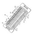
図1、図2は、本発明の一実施形態としての電気コネクタ組立体を構成する。それぞれプラグコネクタ、リセプタクルコネクタの斜視図である。これらプラグコネクタ、リセプタクルコネクタは、それぞれが本発明の電気コネクタの実施形態に相当する。 1 and 2 constitute an electrical connector assembly as an embodiment of the present invention. It is a perspective view of a plug connector and a receptacle connector, respectively. Each of the plug connector and the receptacle connector corresponds to an embodiment of the electrical connector of the present invention.
図1に示すプラグコネクタ10は、2列に配列された信号コンタクト11と、側面視でコ字形をなす接地部材12と、それら信号コンタクト11及び接地部材12を保持するハウジング13から構成されている。
The
ハウジング13は、外周を囲う外壁131と、その内側に立設して一周する内壁132を備えており、その内壁132の内側には、大きな貫通開口133が形成されている。
The
また、信号コンタクト11には、図1に示されている部分として、ハウジング13の内壁131の外側に沿って立ち上がる、相手コネクタのコンタクトに接触する接触部111と、ハウジング13の底部から横に延びてハウジング13から突出した、回路基板(図示せず)に接続される端子部114が設けられている。信号コンタクト11の詳細構造については後述する。
In addition, the
また、接地部材12は、2列に配列された信号コンタクト11のうちの一方の信号コンタクト列11aに近接配置される第1接地プレート121と、他方の信号コンタクト列11bに近接配置される第2接地プレート122と、これら第1接地プレート121及び第2接地プレート122を連結して、プラグコネクタ10が実装される回路基板(ここには図示せず。図3参照)に表面実装される連結部123とからなる。この接地部材12の第1接地プレート121及び第2接地プレート122には、打抜き及び曲げ加工により形成された接地コンタクト124が配列されている。また、この接地部材12の連結部123には、このプラグコネクタ10の裏面に貫通するスリット状の開口125が多数設けられている。この接地部材12には、その連結部123がハウジング13の貫通開口133に配置され、第1接地プレート121及び第2接地プレート222がハウジング13の内壁132の内側に支持された状態に、ハウジング13に保持されている。
The
図2に示すリセプタクルコネクタ20は、2列に配列された多数の信号コンタクト21と、側面視でコ字形をなす接地部材22と、それら信号コンタクト21及び接地部材22を保持するハウジング23から構成されている。
The
ハウジング23には、外周を囲う外壁231が形成されており、またその外壁231で囲われた領域の中央部には、長手方向に延びた貫通開口232が形成されている。
The
このリセプタクルコネクタ20の信号コンタクト21には、図2に示されている部分として、ハウジング23の外壁231の内側に沿って立ち上がる、相手コネクタのコンタクトに接触する接触部211と、ハウジング23の底部から横に延びてハウジング23から突出した、回路基板(図示せず)に接続される端子部214が設けられている。この信号コンタクト21の接触部211は、図1に示すプラグコネクタ10の信号コンタクト11の接触部111と同一形状をなしている。信号コンタクト21の詳細構造については、図1に示すプラグコネクタ10の信号コンタクト11の詳細構造の説明と一緒に後述する。
The
また、接地部材22は、2列に配列された信号コンタクト21のうちの一方の信号コンタクト列21aに近接配置された第1接地プレート221と、他方の信号コンタクト列21bに近接配置された第2接地プレート222と、これら第1接地プレート221及び第2接地プレート222を連結して、このリセプタクルコネクタ20が実装される回路基板(ここには図示せず。図3参照)に表面実装される連結部223とからなる。
The
ここで、図1に示すプラグコネクタ10の接地部材12を構成する第1接地プレート121及び第2接地プレート122はハウジング13の内壁132に支えられているため、このプラグコネクタ10の接地部材12は薄板材料で形成されていたが、図2に示すリセプタクルコネクタ20の接地部材22を構成する第1接地プレート221及び第2接地プレート222はその自体の剛性で立設しており、したがってこのリセプタクルコネクタ20の接地部材22は、図1に示すプラグコネクタ10の接地部材12と比べ厚板の材料で形成されて相対的に大きな剛性を有している。
Here, since the
このように、このリセプタクルコネクタ20の接地部材22は、それ自体で自立できるだけの大きな剛性を有するため、このリセプタクルコネクタ20のハウジング23には、その接地部材22を構成する第1接地プレート221及び第2接地プレート222を支持するための壁を形成する必要がなく、このことにより、このリセプタクルコネクタ20や、このリセプタクルコネクタ20とプラグコネクタ10とを合わせた電気コネクタ組立体の幅方向の寸法を小さく保ち、かつ連結部123,223の視野を良好に保つことができる。
Thus, since the grounding
また、図2に示すリセプタクルコネクタ20を構成する接地部材22の連結部223には、このリセプタクルコネクタ20の裏面に貫通するスリット状の多数の開口224が形成されている。この接地部材22は、その連結部223がハウジング23の貫通開口232に配置された状態に、そのハウジング23に保持されている。
In addition, a large number of slit-shaped
図3は、接地部材の連結部が回路基板に半田付けされた状態を示す模式断面図である。 FIG. 3 is a schematic cross-sectional view showing a state in which the connecting portion of the ground member is soldered to the circuit board.
図1、図2のいずれのコネクタ10,20にも接地部材12,22が備えられており、これらの接地部材12,22の連結部123,223には、裏側に貫通するスリット状の開口125,224が形成されている。
Each of the
図3は、図1に示すプラグコネクタ10の接地部材12で代表させて、その接地部材12の連結部123に多数形成された開口125の1つと、接地部材12の連結部123の、その1つの開口125の両側の部分を示したものである。
FIG. 3 is representative of the grounding
この接地部材12の連結部123は、回路基板30に半田31で半田付けされることにより表面実装されるが、その際、図3に示すように、開口125の周縁部分が回路基板30と半田31で半田付けされる。
The connecting
このように接地部材12(図2に示すリセプタクルコネクタ20の接地部材22も同様)に多数の開口125,224を設けたため、それら多数の開口125,224の縁が半田付けされて全体として強固に且つ確実に半田付けされる。また、この開口125,224は貫通しており、且つ、ハウジング13,23に設けられた貫通開口133,232に配備されているため、接地部材12,22の連結部123,223の半田付けの状態を目視確認することができ、半田付けの信頼性を高めることができる。
As described above, since the large number of
図4、図5は、図1に示すプラグコネクタ10と図2に示すリセプタクルコネクタ20の嵌合状態を示す断面図である。図4は、図2に示すリセプタクルコネクタ20を矢印X−Xに沿って断面し、図1のプラグコネクタ10もそれに対応する箇所を断面して示した図であり、図5は、図2に示すリセプタクルコネクタ20を矢印Y−Yに沿って断面し、図1のプラグコネクタ10もそれに対応する箇所を断面して示した図である。
4 and 5 are cross-sectional views showing a fitting state of the
尚、図4においては、プラグコネクタ10の信号コンタクト11の接触部111及びリセプタクルコネクタ20の信号コンタクト21の接触部211がそれぞれ相手コンタクトに食い込むように描かれているが、これは、嵌合する前のプラグコネクタ10及びリセプタクルコネクタ20の信号コンタクト11,21の接触部111,211の位置を示したものであり、実際には嵌合の際に相手コンタクトと干渉して撓んだ状態となり、相手コンタクトに所定の接触圧をもって接触し電気的に導通した状態に保たれる。
In FIG. 4, the
また、図4においてプラグコネクタ10の接地部材12の接地コンタクト124は、その一部がリセプタクルコンタクト20の接地部材22の第1接地プレート221及び第2接地プレート222に隠れるように描かれており、図5では、接地コンタクト124が第1接地プレート221及び第2接地プレート222に食い込んで描かれているが、これも上記の信号コンタクトの接触部111,211が相手コンタクトに食い込んで描かれているのと同じ理由によるものであり、接地コンタクト124は、実際には、嵌合の際に第1接地プレート221及び第2接地プレート222と干渉して弾性的に変形し所定の接触圧を保って第1接地プレート221及び第2接地プレート222に接触し、プラグコネクタ10及びリセプタクルコンタクト20のグランド同士が接続された状態となる。
In FIG. 4, the
ここで、図4、図5から分かるように一方の信号コンタクト列11a,21aに近接した位置に第1接地プレート121,221からなるグランドの壁が形成されるとともに、他方の信号コンタクト列11b,21bに近接した位置に、第2接地プレート122,222からなるグランドの壁が形成されている。これによりクロストークが抑制され、高速伝送に好適な構造となっている。
Here, as can be seen from FIGS. 4 and 5, a ground wall made up of the
ここで、図4、図5に関する説明を一旦中断し、信号コンタクト11,21自体の構造について先に説明する。
Here, the explanation regarding FIG. 4 and FIG. 5 is temporarily interrupted, and the structure of the
図6は、プラグコネクタ及びリセプタクルコネクタの信号コンタクトを示す斜視図である。 FIG. 6 is a perspective view showing signal contacts of the plug connector and the receptacle connector.
図6に示すように、各信号コンタクト11,21には、接触部111,211、凸部112,212、圧入部113,213及び端子部114,214が形成されている。
As shown in FIG. 6,
接触部111,211は、プラグコネクタ10(図1、図4、図5参照)とリセプタクルコネクタ20(図2、図4、図5参照)が嵌合した際に相手コネクタと干渉して弾性的に変形し、相手コンタクトに対し所定の接触圧を持って接触し、相手コンタクトと電気的に接続される部分である。この接触部111,211の、相手コンタクトと接する面は、元々の金属平板の面(いわゆるロール面)が使われており、その面は平滑面であり、挿抜力の低下及び高い接触信頼性に寄与している。
The
また凸部112,212は、図4に示すように、プラグコネクタ10のハウジング13の内壁132の外側、リセプタクルコネクタ20のハウジング23の外壁231の内側に当接して、接触部111,211をその内壁132、外壁231から離間した状態に置くためのものである。
Further, as shown in FIG. 4, the
接触部111,211は、相手コンタクトの凸部212,112の近傍に接触するように形成されている。これは、凸部212,112が形成された部分は、凸部212,112がハウジングに当接して位置が固定されているため、接触部111,211という弾性部と、凸部212,112近傍の非弾性部とが所定の接触圧を持って接触する状態となり、両コンタクトの接触が安定し確実な電気的導通が図られるからである。
The
図7は、信号コンタクトの凸部の形成方法の説明図である。ここでは、代表的にリセプタクルコネクタ20のコンタクト21について説明する。
FIG. 7 is an explanatory diagram of a method for forming a convex portion of a signal contact. Here, the
先ず、図7(A)に示すように板金の打抜き加工により、幅方向に突出した突出片2121,2122を形成する。その後、これら幅方向に突出した突出片2121,2122を図7(B)に示す矢印方向に折り曲げるとともに内側に寄せる力を加えることにより、凸部212が形成される。プラグコネクタ10のコンタクト11の凸部112についても同様である。
First, as shown in FIG. 7A, protruding
また、図6に示す信号コンタクト11,21の圧入部113,213はハウジング13,23に圧入される部分である。この圧入部113,213は、元々の金属板の幅方向、すなわち、図4、図5における紙面に垂直な方向に広がっており、ハウジング13,23の、図4,図5における紙面に垂直な方向を向いた壁に食い込むことにより固定される。
Further, the press-
また、図6に示す信号コンタクト11,21の端子部114,214は、基板に実装される部分である。ここに示す例では端子部114,214は基板に表面実装される形状を有している。
Further, the
図4及び図5、特に図4に戻って説明を続ける。 Returning to FIG. 4 and FIG. 5, particularly FIG. 4, the description will be continued.
プラグコネクタ10のハウジング13の内壁132の先端、すなわち、そのプラグコネクタ10の信号コンタクト11の接触部111の先端近傍に、その接触部111の先端を保護するための庇部134が形成されている。このプラグコネクタ10のハウジング13の構造の場合、内壁132の外側は、この庇部134以外突出した部分は存在せず、このハウジング13を図4の上下に分割できる割り金型で製造することが可能である。このプラグコネクタ10の信号コンタクト11には、上述の凸部112が設けられているため、その信号コンタクト11の接触部111をハウジング13の壁から離間した状態に保つことができ、しかもその信号コンタクト11の凸部112が形成された部分で相手コンタクトの接触部の接触を安定的に受けることができる。
A
また、リセプタクルコネクタ20についても同様であり、リセプタクルコネクタ20のハウジング23の外壁231の先端、すなわち、そのリセプタクルコネクタ20の信号コンタクト21の接触部211の先端近傍に、その接触部211の先端を保護するための庇部233が形成されている。このリセプタクルコネクタ20のハウジング23の構造の場合、外壁231の内側は、この庇部233以外突出した部分は存在せず、このハウジング23を図4の上下に分割できる割り金型で製造することができる。このリセプタクルコネクタ20の信号コンタクト21には、上述の凸部212が設けられているため、その信号コンタクト21の接触部211をハウジング23の壁から離間した状態に保つことができ、しかも、その信号コンタクト21の凸部212が形成された部分で相手コンタクトの接触部の接触を安定的に受けることができる。
The same applies to the
10 プラグコネクタ
11 信号コンタクト
12 接地部材
13 ハウジング
20 リセプタクルコネクタ
21 信号コンタクト
22 接地部材
23 ハウジング
111 接触部
112 凸部
113 圧入部
114 端子部
121 第1接地プレート
122 第2接地プレート
123 連結部
124 接地コンタクト
125 開口
131 外壁
132 内壁
133 貫通開口
134 庇部
211 接触部
212 凸部
213 圧入部
214 端子部
221 第1接地プレート
222 第2接地プレート
223 連結部
224 開口
231 外壁
232 貫通開口
233 庇部
DESCRIPTION OF
Claims (3)
前記接地部材は、一方の信号コンタクト列に近接配置された第1接地プレートと、他方の信号コンタクト列に近接配置された第2接地プレートと、前記第1及び第2接地プレートを連結して前記電気コネクタが実装される回路基板に表面実装される連結部とからなり、側面視でコ字形をなし、
前記ハウジングは、前記連結部を目視確認できるように前記第1及び第2接地プレート間に貫通開口を有することを特徴とする電気コネクタ。 In an electrical connector comprising signal contacts arranged in two rows, a ground member arranged between the rows of signal contacts, and a housing holding the signal contacts and the ground member,
The ground member connects the first and second ground plates by connecting a first ground plate disposed in proximity to one signal contact row, a second ground plate disposed in proximity to the other signal contact row, and the first and second ground plates. It consists of a connecting part that is surface-mounted on the circuit board on which the electrical connector is mounted.
The electrical connector according to claim 1, wherein the housing has a through opening between the first and second ground plates so that the connecting portion can be visually confirmed.
前記各接地部材は、一方の信号コンタクト列に近接配置された第1接地プレートと、他方の信号コンタクト列に近接配置された第2接地プレートと、前記第1及び第2接地プレートを連結して前記電気コネクタが実装される回路基板に表面実装される連結部とからなり、側面視でコ字形をなし、
前記各ハウジングは、前記連結部を目視確認できるように前記第1及び第2接地プレート間に貫通開口を有することを特徴とする電気コネクタ組立体。 Signal contacts arranged in two rows, grounding members arranged between the rows of signal contacts, and first and second connectors each having a housing for holding the signal contacts and the grounding members and fitting with each other In the electrical connector assembly,
Each of the ground members connects a first ground plate disposed in proximity to one signal contact row, a second ground plate disposed in proximity to the other signal contact row, and the first and second ground plates. It consists of a connecting portion that is surface-mounted on a circuit board on which the electrical connector is mounted, and has a U-shape in side view,
Each of the housings has a through opening between the first and second ground plates so that the connecting portion can be visually confirmed.
Priority Applications (6)
| Application Number | Priority Date | Filing Date | Title |
|---|---|---|---|
| JP2003430610A JP2005190818A (en) | 2003-12-25 | 2003-12-25 | Electrical connector and electrical connector assembly |
| EP04257880A EP1548900A1 (en) | 2003-12-25 | 2004-12-16 | Electrical connector and electrical connector assembly |
| US11/018,021 US6984137B2 (en) | 2003-12-25 | 2004-12-21 | Electrical connector and electrical connector assembly |
| TW093139781A TW200533019A (en) | 2003-12-25 | 2004-12-21 | Electrical connector and electrical connector assembly |
| KR1020040111149A KR20050065388A (en) | 2003-12-25 | 2004-12-23 | Electrical connector and electrical connector assembly |
| CNA200410061520XA CN1638207A (en) | 2003-12-25 | 2004-12-27 | Electrical connector and electrical connector assembly |
Applications Claiming Priority (1)
| Application Number | Priority Date | Filing Date | Title |
|---|---|---|---|
| JP2003430610A JP2005190818A (en) | 2003-12-25 | 2003-12-25 | Electrical connector and electrical connector assembly |
Publications (1)
| Publication Number | Publication Date |
|---|---|
| JP2005190818A true JP2005190818A (en) | 2005-07-14 |
Family
ID=34545032
Family Applications (1)
| Application Number | Title | Priority Date | Filing Date |
|---|---|---|---|
| JP2003430610A Withdrawn JP2005190818A (en) | 2003-12-25 | 2003-12-25 | Electrical connector and electrical connector assembly |
Country Status (6)
| Country | Link |
|---|---|
| US (1) | US6984137B2 (en) |
| EP (1) | EP1548900A1 (en) |
| JP (1) | JP2005190818A (en) |
| KR (1) | KR20050065388A (en) |
| CN (1) | CN1638207A (en) |
| TW (1) | TW200533019A (en) |
Cited By (4)
| Publication number | Priority date | Publication date | Assignee | Title |
|---|---|---|---|---|
| JP2012033439A (en) * | 2010-08-03 | 2012-02-16 | Hirose Electric Co Ltd | Electric connector for circuit substrate |
| JP2015002057A (en) * | 2013-06-14 | 2015-01-05 | 宏致電子股▲ふん▼有限公司Aces Electronics Co.,Ltd. | Electrical connector |
| JP2015005395A (en) * | 2013-06-20 | 2015-01-08 | Smk株式会社 | Connector |
| US9065221B2 (en) | 2012-06-04 | 2015-06-23 | Japan Aviation Electronics Industry, Limited | Connector with metal plate for electro-static discharge protection |
Families Citing this family (13)
| Publication number | Priority date | Publication date | Assignee | Title |
|---|---|---|---|---|
| KR20070014950A (en) * | 2005-07-28 | 2007-02-01 | 교우세라 에르코 가부시키가이샤 | Connector and Handheld Terminal |
| USD580366S1 (en) * | 2008-01-16 | 2008-11-11 | Cheng Uei Precision Industry Co., Ltd. | Receptacle connector |
| USD580365S1 (en) * | 2008-01-16 | 2008-11-11 | Cheng Uei Precision Industry Co., Ltd. | Board-to-board connector |
| JP4726019B2 (en) * | 2008-09-16 | 2011-07-20 | 日本航空電子工業株式会社 | Connector device |
| US20100173507A1 (en) * | 2009-01-07 | 2010-07-08 | Samtec, Inc. | Electrical connector having multiple ground planes |
| US9007783B2 (en) * | 2011-05-31 | 2015-04-14 | Sony Corporation | Memory device and receptacle for electronic devices |
| JP6429263B2 (en) * | 2013-06-19 | 2018-11-28 | 宏致電子股▲ふん▼有限公司Aces Electronics Co.,Ltd. | Connector, connector manufacturing method, and flat cable with connector |
| JP2016152083A (en) * | 2015-02-16 | 2016-08-22 | タイコエレクトロニクスジャパン合同会社 | Connector |
| US10396479B2 (en) * | 2017-01-19 | 2019-08-27 | Murata Manufacturing Co., Ltd. | Multipolar connector set |
| TWI674712B (en) * | 2018-07-06 | 2019-10-11 | 唐虞企業股份有限公司 | Socket connector and electrical connector assembly |
| CN111009760B (en) * | 2018-11-21 | 2021-09-17 | 富鼎精密工业(郑州)有限公司 | Electrical connector |
| CN110098505B (en) * | 2018-11-28 | 2020-10-30 | 番禺得意精密电子工业有限公司 | Electric connector and connector assembly |
| JP1719682S (en) * | 2021-09-30 | 2022-07-13 | electrical connector |
Family Cites Families (35)
| Publication number | Priority date | Publication date | Assignee | Title |
|---|---|---|---|---|
| JP2528234B2 (en) | 1991-05-13 | 1996-08-28 | 富士通株式会社 | Impedance matching type electrical connector |
| JPH0584045U (en) * | 1992-04-18 | 1993-11-12 | モレックス インコーポレーテッド | Thin surface mount electrical connector |
| JPH0794248A (en) * | 1993-09-24 | 1995-04-07 | Kel Corp | Electrical connector |
| US5413491A (en) * | 1993-10-13 | 1995-05-09 | Burndy Corporation | Small form factor connectors with center ground plate |
| US5411404A (en) * | 1993-10-29 | 1995-05-02 | The Whitaker Corporation | Electrical connector having bus bars providing circuit board retention |
| US5536179A (en) * | 1994-07-25 | 1996-07-16 | The Whitaker Corporation | Electrical connector with ground bus insert |
| JP3685210B2 (en) * | 1994-11-11 | 2005-08-17 | ケル株式会社 | connector |
| JP3631312B2 (en) * | 1995-12-22 | 2005-03-23 | 富士通コンポーネント株式会社 | High-speed signal connector |
| US6015304A (en) * | 1995-12-29 | 2000-01-18 | Molex Incorporated | Ground-enhanced electrical connector |
| US6019616A (en) * | 1996-03-01 | 2000-02-01 | Molex Incorporated | Electrical connector with enhanced grounding characteristics |
| JP3148855B2 (en) * | 1996-03-01 | 2001-03-26 | モレックス インコーポレーテッド | Electrical connector |
| US5921787A (en) * | 1996-07-17 | 1999-07-13 | Minnesota Mining And Manufacturing Company | Board-to-board interconnection |
| US5697799A (en) | 1996-07-31 | 1997-12-16 | The Whitaker Corporation | Board-mountable shielded electrical connector |
| US5813871A (en) * | 1996-07-31 | 1998-09-29 | The Whitaker Corporation | High frequency electrical connector |
| CN2313311Y (en) * | 1996-12-30 | 1999-04-07 | 鸿海精密工业股份有限公司 | electrical connector |
| US5915976A (en) * | 1997-02-06 | 1999-06-29 | Hon Hai Precision Ind. Co., Ltd. | High speed connector |
| TW330737U (en) * | 1997-06-05 | 1998-04-21 | Hon Hai Prec Ind Co Ltd | Connector for high density plugs |
| TW368212U (en) * | 1997-08-16 | 1999-08-21 | Hon Hai Prec Ind Co Ltd | Plate-to-plate electric connector |
| JP3277154B2 (en) * | 1998-05-06 | 2002-04-22 | ケル株式会社 | connector |
| US6338635B1 (en) * | 2000-08-01 | 2002-01-15 | Hon Hai Precision Ind. Co., Ltd. | Electrical connector with improved grounding bus |
| US6290515B1 (en) * | 2000-09-05 | 2001-09-18 | Hon Hai Precision Ind. Co., Ltd. | Electrical connector assembly having grounding buses |
| US20020115318A1 (en) * | 2001-01-02 | 2002-08-22 | Apicelli Samuel W. | Electrical connector and circuit with center ground plane |
| TW475786U (en) * | 2001-02-27 | 2002-02-01 | Hon Hai Prec Ind Co Ltd | Electrical connector assembly |
| US6503101B1 (en) * | 2001-12-04 | 2003-01-07 | Hon Hai Precision Ind. Co., Ltd. | Electrical connector having grounding path |
| US6572410B1 (en) * | 2002-02-20 | 2003-06-03 | Fci Americas Technology, Inc. | Connection header and shield |
| US6685485B2 (en) * | 2002-03-07 | 2004-02-03 | Hon Hai Precision Ind. Co., Ltd. | Electrical connector |
| US6688897B2 (en) * | 2002-03-07 | 2004-02-10 | Hon Hai Precision Ind. Co., Ltd. | Electrical connector |
| TW532587U (en) * | 2002-03-13 | 2003-05-11 | Hon Hai Prec Ind Co Ltd | Electrical connector couple |
| US6648657B1 (en) * | 2002-06-10 | 2003-11-18 | Hon Hai Precision Ind. Co., Ltd. | Electrical connector having ground buses |
| TW553540U (en) * | 2002-12-13 | 2003-09-11 | Hon Hai Prec Ind Co Ltd | Electrical connector assembly |
| US6663402B1 (en) * | 2003-01-08 | 2003-12-16 | Hon Hai Precision Ind. Co., Ltd. | Electrical connector having grounding bridge |
| US6726492B1 (en) * | 2003-05-30 | 2004-04-27 | Hon Hai Precision Ind. Co., Ltd. | Grounded electrical connector |
| TWM250431U (en) * | 2003-08-08 | 2004-11-11 | Hon Hai Prec Ind Co Ltd | Electrical connector |
| US6884094B1 (en) * | 2003-11-10 | 2005-04-26 | Tyco Electronics Corporation | Connector with hermaphroditic center ground plane |
| JP2005190815A (en) * | 2003-12-25 | 2005-07-14 | Tyco Electronics Amp Kk | Electric connector assembly |
-
2003
- 2003-12-25 JP JP2003430610A patent/JP2005190818A/en not_active Withdrawn
-
2004
- 2004-12-16 EP EP04257880A patent/EP1548900A1/en not_active Withdrawn
- 2004-12-21 US US11/018,021 patent/US6984137B2/en not_active Expired - Fee Related
- 2004-12-21 TW TW093139781A patent/TW200533019A/en unknown
- 2004-12-23 KR KR1020040111149A patent/KR20050065388A/en not_active Withdrawn
- 2004-12-27 CN CNA200410061520XA patent/CN1638207A/en active Pending
Cited By (5)
| Publication number | Priority date | Publication date | Assignee | Title |
|---|---|---|---|---|
| JP2012033439A (en) * | 2010-08-03 | 2012-02-16 | Hirose Electric Co Ltd | Electric connector for circuit substrate |
| US9065221B2 (en) | 2012-06-04 | 2015-06-23 | Japan Aviation Electronics Industry, Limited | Connector with metal plate for electro-static discharge protection |
| JP2015002057A (en) * | 2013-06-14 | 2015-01-05 | 宏致電子股▲ふん▼有限公司Aces Electronics Co.,Ltd. | Electrical connector |
| JP2015005395A (en) * | 2013-06-20 | 2015-01-08 | Smk株式会社 | Connector |
| US9196987B2 (en) | 2013-06-20 | 2015-11-24 | Smk Corporation | Connector |
Also Published As
| Publication number | Publication date |
|---|---|
| TW200533019A (en) | 2005-10-01 |
| US6984137B2 (en) | 2006-01-10 |
| US20050142909A1 (en) | 2005-06-30 |
| EP1548900A1 (en) | 2005-06-29 |
| CN1638207A (en) | 2005-07-13 |
| KR20050065388A (en) | 2005-06-29 |
Similar Documents
| Publication | Publication Date | Title |
|---|---|---|
| CN110911865B (en) | Electrical connector for circuit board and electrical connector mounting body for circuit board | |
| JP5790245B2 (en) | Coaxial electrical connector and coaxial electrical connector assembly | |
| JP2005190818A (en) | Electrical connector and electrical connector assembly | |
| KR101397761B1 (en) | Electronic component | |
| KR20080033860A (en) | Contact and Electrical Connectors | |
| JP2012156090A (en) | Floating type connector | |
| JP2016110966A (en) | Contact and connector employing the contact | |
| JP2011146210A (en) | Electric connector | |
| JP2018092780A (en) | Connector device with prevention structure | |
| JP4365422B2 (en) | Connector and portable terminal equipped with connector | |
| JP2005190815A (en) | Electric connector assembly | |
| JP5787081B2 (en) | Connector device | |
| JPH11144823A (en) | Printed circuit board connector and its mounting structure | |
| JP7640770B2 (en) | Connector set and connector | |
| JP2008171627A (en) | Female terminal fitting | |
| US6558171B2 (en) | Printed board connector, contact thereof and mating instrument | |
| JP3707016B2 (en) | connector | |
| JP2014229383A (en) | Connector for substrate | |
| JP5344992B2 (en) | Internal terminals of circuit board connector | |
| JP2011003393A (en) | Connector device | |
| JPH07230858A (en) | Movable connector | |
| CN220934443U (en) | Electrical connector | |
| JP2010287356A (en) | Connector | |
| JP2011165357A (en) | Connector apparatus | |
| JP2018185887A (en) | connector |
Legal Events
| Date | Code | Title | Description |
|---|---|---|---|
| A621 | Written request for application examination |
Free format text: JAPANESE INTERMEDIATE CODE: A621 Effective date: 20061127 |
|
| A761 | Written withdrawal of application |
Free format text: JAPANESE INTERMEDIATE CODE: A761 Effective date: 20071102 |