JP2005183444A - Substrate holding carrier and substrate holding and carrying method - Google Patents
Substrate holding carrier and substrate holding and carrying method Download PDFInfo
- Publication number
- JP2005183444A JP2005183444A JP2003417992A JP2003417992A JP2005183444A JP 2005183444 A JP2005183444 A JP 2005183444A JP 2003417992 A JP2003417992 A JP 2003417992A JP 2003417992 A JP2003417992 A JP 2003417992A JP 2005183444 A JP2005183444 A JP 2005183444A
- Authority
- JP
- Japan
- Prior art keywords
- substrate
- substrate holding
- carrier
- holding carrier
- silicon wafer
- Prior art date
- Legal status (The legal status is an assumption and is not a legal conclusion. Google has not performed a legal analysis and makes no representation as to the accuracy of the status listed.)
- Pending
Links
Images


Abstract
Description
本発明は、シリコンウエハ上に集積回路を形成する工程等において、シリコンウエハ等の基板を保持、搬送するための基板保持キャリア及び基板の保持搬送方法に関する。 The present invention relates to a substrate holding carrier for holding and transferring a substrate such as a silicon wafer and a method for holding and transferring the substrate in a process of forming an integrated circuit on a silicon wafer.
現在、例えばシリコンウエハ等のウエハは、集積回路(以下、ICと省略する。)が形成されてチップ状に加工等がされることによって、さまざまな電子機器に使用されている。近年、ICの更なる小型化が進んでおり、例えば、ICチップを積層することで高密度化を実現したスタックドICにおいても、よりICを高密度に配置するため、より多層構造とすることが求められている。 Currently, for example, a wafer such as a silicon wafer is used in various electronic devices by forming an integrated circuit (hereinafter abbreviated as IC) and processing it into a chip shape. In recent years, further miniaturization of ICs has progressed. For example, even in a stacked IC in which high density is realized by stacking IC chips, in order to arrange the ICs at a higher density, a more multilayer structure may be used. It has been demanded.
そこで、より薄いシリコンウエハを用い、そのシリコンウエハ上にICを製作することによって、積層数の増加や全体の厚さ低減を図り、より多層の構造とすることが可能となる。従来、シリコンウエハが0.2mm程度の厚さであれば、現在主に用いられているようなICの製造ラインにシリコンウエハをそのまま投入している。しかし、0.1mm以下、特に0.05mm程度の厚さになると極薄のため、ハンドリング等の関係上強度不足等の理由から従来のICの製造ラインに投入することが困難となる。 Therefore, by using a thinner silicon wafer and manufacturing an IC on the silicon wafer, it is possible to increase the number of stacked layers and reduce the overall thickness, thereby obtaining a multilayer structure. Conventionally, when a silicon wafer has a thickness of about 0.2 mm, the silicon wafer is put into an IC manufacturing line that is mainly used at present. However, when the thickness is 0.1 mm or less, particularly about 0.05 mm, it is extremely thin, and it is difficult to put it into a conventional IC production line because of insufficient strength due to handling and the like.
一方、例えばフィルム上の絶縁基板表面に導体パターンを備えたフレキシブルプリント配線板(以下、FPCと省略する。)等の薄板のプリント配線板表面に電子部品等を実装する工程や、プリント配線板を製造する工程において高効率生産を実現するための保持搬送用キャリアが提案されている(例えば、特許文献1参照。)。
この保持搬送用キャリアは、硬質のベース材とベース材の表面にコーティングされた自己粘着性を有する例えばフッ素樹脂、またはシリコーン系樹脂の薄層とを備えており、フッ素樹脂、またはシリコーン樹脂薄層の上にプリント基板を載置することでプリント基板を保持搬送することができる。
The carrier for holding and transporting includes a hard base material and a thin layer of, for example, a fluororesin or a silicone resin having a self-adhesive property coated on the surface of the base material. By placing the printed circuit board on the printed circuit board, the printed circuit board can be held and conveyed.
しかしながら、上記従来技術には、以下の課題が残されている。すなわち、シリコンウエハのハンドリングにおいてより積層数の高いスタックドICには薄厚化の要望があり、シリコンウエハの厚さが0.1mm以下、特に0.05mm程度の厚さになると極薄のため、従来のようなシリコンウエハをそのまま扱うハンドリング等ではシリコンウエハの強度不足等の理由からそのままでは従来のIC製造ラインに投入することができなくなる。
そこで、従来のFPC用の保持搬送キャリアにシリコンウエハを載置して搬送することも考えられるが、FPCを保持搬送用キャリアから剥離する際、柔らかいFPCを引っ張り上げて曲げて剥離したが、上記従来の保持搬送用キャリアに載置したシリコンウエハを保持搬送用キャリアから剥離する際に、シリコンウエハは薄くてもFPC等と比べて高い硬度を有しているため、シリコンウエハが破損してしまうという虞があった。
However, the following problems remain in the prior art. That is, there is a demand for a thinner stacked IC having a higher number of stacked silicon wafers, and when the thickness of the silicon wafer is 0.1 mm or less, particularly about 0.05 mm, it is extremely thin. In handling such a silicon wafer as it is, it cannot be put into a conventional IC manufacturing line as it is because of insufficient strength of the silicon wafer.
Therefore, it is conceivable to place and transfer a silicon wafer on a conventional FPC holding carrier carrier, but when peeling the FPC from the carrier carrier, the soft FPC is pulled up and bent to peel off. When a silicon wafer placed on a conventional carrier for holding and transporting is peeled from the carrier for holding and transporting, even if the silicon wafer is thin, the silicon wafer has a higher hardness than FPC and the like, so the silicon wafer is damaged. There was a fear.
本発明は、前述の課題に鑑みてなされたもので、薄いウエハを破損せずに保持、搬送を行うことができる基板保持キャリア及び基板の保持搬送方法を提供することを目的とする。 The present invention has been made in view of the above-described problems, and an object of the present invention is to provide a substrate holding carrier and a substrate holding and conveying method capable of holding and transferring a thin wafer without damaging it.
本発明は、前記課題を解決するために以下の構成を採用した。すなわち、本発明の基板保持キャリアは、基板を基板載置面で保持するプレート状の基板保持キャリアであって、前記基板載置面が自己粘着性を有し、全体が前記基板よりも高い可撓性を有していることを特徴とする。 The present invention employs the following configuration in order to solve the above problems. That is, the substrate holding carrier of the present invention is a plate-like substrate holding carrier that holds a substrate on the substrate mounting surface, and the substrate mounting surface is self-adhesive, and the whole is higher than the substrate. It is characterized by having flexibility.
この発明によれば、自己粘着性を有する基板載置面に基板を載置することによって基板のみを搬送するときに比べ、基板にかかる外力に対する強度を増加させ、保持搬送させたときの基板の破損を抑制する。したがって、極薄で可撓性の小さい基板であってもICの製造ラインに投入することができる。また、基板よりも高い可撓性を有しているため、基板から剥離する際に基板保持キャリアを曲げて基板から剥離することで、基板の破損を防止することができる。 According to the present invention, compared with the case where only the substrate is transported by placing the substrate on the self-adhesive substrate placement surface, the strength against the external force applied to the substrate is increased, and the substrate when it is held and transported is increased. Suppress damage. Therefore, even a very thin and flexible substrate can be put into an IC manufacturing line. Further, since it has higher flexibility than the substrate, it is possible to prevent the substrate from being damaged by bending the substrate holding carrier and peeling from the substrate when peeling from the substrate.
また、本発明に係る基板保持キャリアは、フッ素系の樹脂材料で構成されていることが好ましい。
また、本発明に係る基板保持キャリアは、シリコーン系の樹脂材料で構成されていることが好ましい。
この発明によれば、フッ素系の樹脂材料またはシリコーン系の樹脂材料によって構成することで、耐熱性を向上させることができる。
The substrate holding carrier according to the present invention is preferably made of a fluorine-based resin material.
Further, the substrate holding carrier according to the present invention is preferably made of a silicone-based resin material.
According to this invention, heat resistance can be improved by comprising with a fluorine-type resin material or a silicone-type resin material.
また、本発明に係る基板保持キャリアは、前記可撓性を有するベース層と、該ベース層上に設けられ前記基板載置面を有する自己粘着性層とから構成されていることが好ましい。
この発明によれば、上述と同様に極薄で可撓性の小さい基板であってもICの製造ラインに投入することができる。
Further, the substrate holding carrier according to the present invention is preferably composed of the flexible base layer and a self-adhesive layer provided on the base layer and having the substrate mounting surface.
According to the present invention, even an extremely thin and flexible substrate as described above can be put into an IC manufacturing line.
また、本発明に係る保持搬送方法は、基板保持キャリアの前記基板載置面に基板を載置して保持搬送する保持搬送工程と、基板載置面に載置した基板を前記基板保持キャリアから剥離する剥離工程とを備え、該剥離工程は、前記基板に対して前記基板保持キャリアを周縁から曲げながら剥離することを特徴とする。
この発明によれば、自己粘着性を有する基板載置面に基板を載置させることで極薄の基板であってもICの製造ライン上で保持搬送できると共に、基板よりも可撓性を有する基板保持キャリアを曲げて基板を剥離することで、基板の破損を防止することができる。
The holding and conveying method according to the present invention includes a holding and conveying step of placing and holding a substrate on the substrate placement surface of a substrate holding carrier, and a substrate placed on the substrate placement surface from the substrate holding carrier. A peeling step for peeling off, wherein the peeling step peels off the substrate holding carrier from the periphery while bending the substrate holding carrier.
According to the present invention, a substrate is placed on a self-adhesive substrate placement surface, so that even an extremely thin substrate can be held and conveyed on an IC production line, and more flexible than a substrate. The substrate can be prevented from being damaged by bending the substrate holding carrier and peeling the substrate.
また、本発明に係る保持搬送方法は、前記基板の前記基板載置面に接着されていた面をプラズマ洗浄による洗浄工程を備えていることを特徴とする。
剥離工程により基板載置面に接着されていた面に基板載置面の自己粘着性材料が付着することがある。
この発明によれば、プラズマを照射するプラズマ洗浄を行うことによって、付着した自己粘着性材料を除去することができる。
Further, the holding and conveying method according to the present invention is characterized in that the surface of the substrate bonded to the substrate mounting surface is provided with a cleaning step by plasma cleaning.
The self-adhesive material of the substrate mounting surface may adhere to the surface that has been bonded to the substrate mounting surface by the peeling process.
According to the present invention, the attached self-adhesive material can be removed by performing plasma cleaning with plasma irradiation.
本発明の基板保持キャリア及び保持搬送方法によれば、自己粘着性を有した基板載置面に基板を載置して保持することによって、搬送の際の外力に対する強度を増加させることができる。また、基板保持キャリア側の可撓性が高いので、基板保持キャリア側を曲げることで基板から剥離させる際の基板の破損を防ぐことができる。したがって、極薄の基板であってもICの製造ラインに投入することができる。 According to the substrate holding carrier and the holding and conveying method of the present invention, the strength against an external force during conveyance can be increased by placing and holding a substrate on a self-adhesive substrate placing surface. Further, since the flexibility of the substrate holding carrier side is high, it is possible to prevent the substrate from being damaged when being peeled from the substrate by bending the substrate holding carrier side. Therefore, even a very thin substrate can be put into the IC production line.
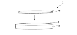
以下、本発明に係る基板保持キャリアの第1の実施形態を、図1を参照しながら説明する。
本実施形態による基板保持キャリア1は、図1に示されるように、例えば直径3〜20インチのシリコンウエハの基板を保持搬送するキャリアであって、一方の面が基板を載置する基板載置面2とされた円盤状の自己粘着層3によって構成されている。
Hereinafter, a first embodiment of a substrate holding carrier according to the present invention will be described with reference to FIG.
As shown in FIG. 1, the substrate holding carrier 1 according to the present embodiment is a carrier that holds and conveys a silicon wafer substrate having a diameter of, for example, 3 to 20 inches. It is comprised by the disk-shaped self-
自己粘着層3は、シリコーン樹脂又はフッ素樹脂で形成されており、また、基板載置面2が、直径3〜20インチであって、自己粘着層3の厚さ寸法が、0.6〜30mmとなっている。
また、基板載置面2は、10〜1000g/cm2を満足する弱粘着性を有している。
The self-
The
次に、以上の構成からなる本実施形態の基板保持キャリア1を用いた基板の保持搬送方法について図2から図6を参照して説明する。
なお、本実施形態ではスピンコーティングによってシリコンウエハ上にレジストを塗布するレジスト塗布工程とする。
先ず、保持搬送工程(S1)を行う。この保持搬送工程(S1)は、図3に示されるように、シリコンウエハWを基板載置面2に載置することでシリコンウエハWを保持する。すなわち、基板載置面2が弱粘着性を有しているためシリコンウエハWを保持でき、搬送や振動に対してシリコンウエハWが基板保持キャリア1からずれたり外れたりすることがない。次に、基板保持キャリア1を搬送してスピンコーティング台5に基板保持キャリア1を載置させる。
Next, a method for holding and transporting a substrate using the substrate holding carrier 1 of the present embodiment having the above configuration will be described with reference to FIGS.
In the present embodiment, a resist coating process is performed in which a resist is coated on a silicon wafer by spin coating.
First, a holding conveyance process (S1) is performed. In the holding and conveying step (S1), the silicon wafer W is held by placing the silicon wafer W on the
続いて、レジスト塗布工程(S2)を行う。このレジスト塗布工程(S2)は、シリコンウエハWの表面にレジストを滴下し、スピンコーティング台5の中心点Pを回転中心として高速回転させることで図4に示すように、シリコンウエハW上に均一に塗布されたレジスト膜6が形成される。このとき、スピンコーティング台5に設けられた吸引口5Aより吸引ポンプ(図示略。)によって吸引されることで基板保持キャリア1がスピンコーティング台5に保持されている。
レジスト膜6の形成後、例えば、250℃、1時間のベーキング処理を施すことによりレジスト膜6を硬化させる。
Subsequently, a resist coating step (S2) is performed. In this resist coating step (S2), a resist is dropped on the surface of the silicon wafer W and rotated at high speed around the center point P of the spin coating table 5 as shown in FIG. A
After the
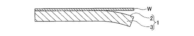
続いて、剥離工程(S3)を行う。この剥離工程(S3)は、図5に示すように、シリコンウエハW側ではなく、基板保持キャリア1を曲げることによりシリコンウエハWを剥離させる。
続いて、洗浄工程(S4)を行う。基板保持キャリア1から剥離されたシリコンウエハWには、図6に示されるように、シリコンウエハWの基板載置面2に載置された面上に自己粘着性材料3Aが付着することがある。この洗浄工程(S4)は、この付着した自己粘着性材料3Aに対しプラズマ洗浄を行う。このプラズマ洗浄は、例えば、アシストガスとしてHe、CF4、O2を用い、出力1500W、搬送スピード0.5m/分とする条件下で自己粘着性材料3Aを除去する。
Then, a peeling process (S3) is performed. In this peeling step (S3), as shown in FIG. 5, the silicon wafer W is peeled by bending the substrate holding carrier 1 instead of the silicon wafer W side.
Subsequently, a cleaning step (S4) is performed. As shown in FIG. 6, the self-
この基板保持キャリア1によるシリコンウエハの保持搬送方法によれば、シリコンウエハWを載置する基板載置面2が自己粘着性を有し、また基板保持キャリア1がシリコンウエハWよりも高い可撓性を有している。したがって、基板保持キャリア1にシリコンウエハWを載置させることでシリコンウエハWの搬送においてシリコンウエハWの破損を防止することができる。また、基板保持キャリア1の方を曲げることでシリコンウエハWを破損させることなく剥離させることができる。
更に、このときシリコンウエハWに付着した自己粘着性材料3Aをプラズマ洗浄により選択的に自己粘着性材料3Aを除去することができる。
また、自己粘着層3にシリコーン樹脂を用いた場合には連続耐熱温度が約200℃であり、フッ素樹脂を用いた場合には信連続体熱温度が約250℃以上であるので、シリコーン樹脂に比べて耐熱性が約50℃向上する。
According to the method of holding and transporting a silicon wafer by the substrate holding carrier 1, the
Furthermore, the self-
Further, when a silicone resin is used for the self-
次に、第2の実施形態について図7を参照しながら説明する。
なお、ここで説明する実施形態はその基本的構成が上述した第1の実施形態と同様であり、上述の第1の実施形態に別の要素を付加したものである。したがって、図7においては、図1と同一構成要素に同一符号をし、この説明を省略する。
Next, a second embodiment will be described with reference to FIG.
The basic configuration of the embodiment described here is the same as that of the first embodiment described above, and another element is added to the first embodiment described above. Therefore, in FIG. 7, the same components as those in FIG.
第2の実施形態と第1の実施形態との異なる点は、第1の実施形態の基板保持キャリア1では基板載置面2を有する自己粘着層3によって構成されているのに対して、第2の実施形態における基板保持キャリア10では、シリコーン樹脂又はフッ素樹脂で構成された可撓性を有するベース層11と、基板載置面12を有する自己粘着層13とによって構成されている点である。
ベース層11は、ガラスクロス、エポキシ樹脂積層材、ステンレス、アルミ、マグネシウム合金材等が用いられている。
The difference between the second embodiment and the first embodiment is that the substrate holding carrier 1 of the first embodiment is constituted by the self-
The
この基板保持キャリア10は、ベース層11と自己粘着層13とで構成されているので、シリコンウエハWの保持に対して最適な弱粘着性を有する自己粘着層13を選択すると共に粘着性にかかわらず全体として基板に対して最適な可撓性を設定可能なベース層11とを分けて構成することができる。したがって、それぞれの自己粘着性と可撓性とを最適にすることができる。
Since the
なお、本発明は上記実施形態に限定されるものではなく、本発明の趣旨を逸脱しない範囲において種々の変更を加えることが可能である。
例えば、上記実施形態では、基板載置面の自己粘着性が均一であったが、これに限らず、例えば半径方向で中心から離間するにしたがって自己粘着性が減少するような構成であってもよい。このようにすることで、基板保持搬送キャリアをシリコンウエハから剥離することが容易となる。
また、第2の実施形態では、ベース層が、例えばガラスクロスをシリコーン系樹脂又はフッ化系樹脂で挟むような多層構造であってもよい。
In addition, this invention is not limited to the said embodiment, A various change can be added in the range which does not deviate from the meaning of this invention.
For example, in the above embodiment, the self-adhesiveness of the substrate mounting surface is uniform. However, the present invention is not limited to this. For example, the self-adhesiveness may be reduced as the distance from the center in the radial direction decreases. Good. By doing in this way, it becomes easy to peel a board | substrate holding | maintenance conveyance carrier from a silicon wafer.
In the second embodiment, the base layer may have a multilayer structure in which, for example, a glass cloth is sandwiched between a silicone resin or a fluorinated resin.
1、10 基板保持キャリア
3 自己粘着層
2 基板載置面
3A 自己粘着性材料
W シリコンウエハ
1, 10
Claims (6)
前記基板載置面が自己粘着性を有し、全体が前記基板よりも高い可撓性を有していることを特徴とする基板保持キャリア。 A plate-like substrate holding carrier for holding a substrate on a substrate mounting surface,
The substrate holding carrier, wherein the substrate mounting surface has self-adhesiveness, and the whole has higher flexibility than the substrate.
基板載置面に載置した基板を前記基板保持キャリアから剥離する剥離工程とを備え、
該剥離工程は、前記基板に対して前記基板保持キャリアを周縁から曲げながら剥離することを特徴とする基板の保持搬送方法。 A holding and conveying step of placing and holding and conveying a substrate on the substrate placement surface of the substrate holding carrier according to any one of claims 1 to 4,
A peeling step of peeling the substrate placed on the substrate placement surface from the substrate holding carrier,
In the peeling step, the substrate holding carrier is peeled off while bending the substrate holding carrier from the periphery.
Priority Applications (1)
| Application Number | Priority Date | Filing Date | Title |
|---|---|---|---|
| JP2003417992A JP2005183444A (en) | 2003-12-16 | 2003-12-16 | Substrate holding carrier and substrate holding and carrying method |
Applications Claiming Priority (1)
| Application Number | Priority Date | Filing Date | Title |
|---|---|---|---|
| JP2003417992A JP2005183444A (en) | 2003-12-16 | 2003-12-16 | Substrate holding carrier and substrate holding and carrying method |
Publications (1)
| Publication Number | Publication Date |
|---|---|
| JP2005183444A true JP2005183444A (en) | 2005-07-07 |
Family
ID=34780317
Family Applications (1)
| Application Number | Title | Priority Date | Filing Date |
|---|---|---|---|
| JP2003417992A Pending JP2005183444A (en) | 2003-12-16 | 2003-12-16 | Substrate holding carrier and substrate holding and carrying method |
Country Status (1)
| Country | Link |
|---|---|
| JP (1) | JP2005183444A (en) |
Cited By (8)
| Publication number | Priority date | Publication date | Assignee | Title |
|---|---|---|---|---|
| WO2008149506A1 (en) * | 2007-06-08 | 2008-12-11 | Hoya Candeo Optronics Corporation | Wafer supporting glass |
| JP2011018769A (en) * | 2009-07-09 | 2011-01-27 | Shin Etsu Polymer Co Ltd | Size adjustment jig for substrate |
| JP2011108738A (en) * | 2009-11-13 | 2011-06-02 | Shin Etsu Polymer Co Ltd | Method for handling of semiconductor wafer |
| WO2011142280A1 (en) * | 2010-05-11 | 2011-11-17 | 旭硝子株式会社 | Process for producing laminate, and laminate |
| JP2013187453A (en) * | 2012-03-09 | 2013-09-19 | Disco Abrasive Syst Ltd | Grinding method for plate-like object |
| JP2014038903A (en) * | 2012-08-13 | 2014-02-27 | Disco Abrasive Syst Ltd | Wafer processing method |
| CN114217207A (en) * | 2021-12-02 | 2022-03-22 | 何志 | Intelligent separation equipment for integrated circuit test |
| WO2023125502A1 (en) * | 2021-12-29 | 2023-07-06 | 北京北方华创微电子装备有限公司 | Base grounding detection apparatus and method |
-
2003
- 2003-12-16 JP JP2003417992A patent/JP2005183444A/en active Pending
Cited By (10)
| Publication number | Priority date | Publication date | Assignee | Title |
|---|---|---|---|---|
| WO2008149506A1 (en) * | 2007-06-08 | 2008-12-11 | Hoya Candeo Optronics Corporation | Wafer supporting glass |
| JP2011018769A (en) * | 2009-07-09 | 2011-01-27 | Shin Etsu Polymer Co Ltd | Size adjustment jig for substrate |
| JP2011108738A (en) * | 2009-11-13 | 2011-06-02 | Shin Etsu Polymer Co Ltd | Method for handling of semiconductor wafer |
| WO2011142280A1 (en) * | 2010-05-11 | 2011-11-17 | 旭硝子株式会社 | Process for producing laminate, and laminate |
| JP5835214B2 (en) * | 2010-05-11 | 2015-12-24 | 旭硝子株式会社 | LAMINATE MANUFACTURING METHOD AND LAMINATE |
| JP2013187453A (en) * | 2012-03-09 | 2013-09-19 | Disco Abrasive Syst Ltd | Grinding method for plate-like object |
| KR101873603B1 (en) | 2012-03-09 | 2018-07-02 | 가부시기가이샤 디스코 | Method for grinding plate-like object |
| JP2014038903A (en) * | 2012-08-13 | 2014-02-27 | Disco Abrasive Syst Ltd | Wafer processing method |
| CN114217207A (en) * | 2021-12-02 | 2022-03-22 | 何志 | Intelligent separation equipment for integrated circuit test |
| WO2023125502A1 (en) * | 2021-12-29 | 2023-07-06 | 北京北方华创微电子装备有限公司 | Base grounding detection apparatus and method |
Similar Documents
| Publication | Publication Date | Title |
|---|---|---|
| JP4306795B2 (en) | WIRING BOARD, SEMICONDUCTOR PACKAGE, ELECTRONIC DEVICE, AND WIRING BOARD MANUFACTURING METHOD | |
| TW200305235A (en) | Releasing layer transfer film and laminate film | |
| JP3585904B2 (en) | Jig for holding and transporting | |
| JP2012033737A (en) | Method for handling semiconductor wafer | |
| TW201233276A (en) | Method of manufacturing electronic component embedded rigid-flexible printed circuit board | |
| JP2007287953A (en) | Circuit board and its production method | |
| JP2005183444A (en) | Substrate holding carrier and substrate holding and carrying method | |
| JP4306540B2 (en) | Thin processing method of semiconductor substrate | |
| JP5843709B2 (en) | Manufacturing method of semiconductor package | |
| JP2008147498A (en) | Multilayer wiring board, and semiconductor device package | |
| JP2006190885A (en) | Substrate for layer formation, wiring substrate and its manufacturing method, and semiconductor device and its manufacturing method | |
| JP2008034790A (en) | Structure combining ic integrated substrate and carrier, manufacturing method thereof, and method of manufacturing electronic device | |
| TWI393494B (en) | Substrate strip with wiring and method for fabricating the same | |
| JP2010108964A (en) | Method for manufacturing circuit board | |
| JP2008078522A (en) | Carrier jig for flexible wiring substrate and electronic parts mounting method using the same | |
| JP2013115315A (en) | Manufacturing method of wiring board | |
| JP2009099834A (en) | Flexible substrate | |
| JP4345464B2 (en) | Method for manufacturing circuit board member to which electronic component is bonded | |
| JP7443689B2 (en) | Manufacturing method of electronic component built-in board | |
| JP2005183424A (en) | Thin substrate fixing jig | |
| JP3604348B2 (en) | Method of reducing warpage of electronic component mounting board | |
| JP2004363438A (en) | Circuit board holding tool | |
| JP2005340390A (en) | Device and method for manufacturing semiconductor device | |
| JP2007194324A (en) | Member for circuit board, and its manufacturing method | |
| JP2005268540A (en) | Manufacturing method of etching article |
Legal Events
| Date | Code | Title | Description |
|---|---|---|---|
| A02 | Decision of refusal |
Free format text: JAPANESE INTERMEDIATE CODE: A02 Effective date: 20050104 |
|
| A521 | Written amendment |
Free format text: JAPANESE INTERMEDIATE CODE: A523 Effective date: 20050331 |
|
| A911 | Transfer of reconsideration by examiner before appeal (zenchi) |
Free format text: JAPANESE INTERMEDIATE CODE: A911 Effective date: 20050405 |
|
| A912 | Removal of reconsideration by examiner before appeal (zenchi) |
Free format text: JAPANESE INTERMEDIATE CODE: A912 Effective date: 20050930 |