JP2005149199A - Texture processor - Google Patents
Texture processor Download PDFInfo
- Publication number
- JP2005149199A JP2005149199A JP2003386769A JP2003386769A JP2005149199A JP 2005149199 A JP2005149199 A JP 2005149199A JP 2003386769 A JP2003386769 A JP 2003386769A JP 2003386769 A JP2003386769 A JP 2003386769A JP 2005149199 A JP2005149199 A JP 2005149199A
- Authority
- JP
- Japan
- Prior art keywords
- texture
- data
- texture data
- memory
- memories
- Prior art date
- Legal status (The legal status is an assumption and is not a legal conclusion. Google has not performed a legal analysis and makes no representation as to the accuracy of the status listed.)
- Granted
Links
- 230000015654 memory Effects 0.000 claims abstract description 225
- 238000001914 filtration Methods 0.000 claims abstract description 46
- 238000012545 processing Methods 0.000 claims abstract description 42
- 238000010586 diagram Methods 0.000 description 19
- 238000000034 method Methods 0.000 description 17
- 238000012546 transfer Methods 0.000 description 16
- 238000003860 storage Methods 0.000 description 7
- 238000013507 mapping Methods 0.000 description 5
- 230000004913 activation Effects 0.000 description 3
- 238000006243 chemical reaction Methods 0.000 description 3
- 238000007796 conventional method Methods 0.000 description 3
- 238000004519 manufacturing process Methods 0.000 description 2
- 238000005070 sampling Methods 0.000 description 2
- 101100365384 Mus musculus Eefsec gene Proteins 0.000 description 1
- 238000005520 cutting process Methods 0.000 description 1
- 230000006870 function Effects 0.000 description 1
- 230000000630 rising effect Effects 0.000 description 1
- 230000011218 segmentation Effects 0.000 description 1
Images


Classifications
-
- G—PHYSICS
- G06—COMPUTING; CALCULATING OR COUNTING
- G06T—IMAGE DATA PROCESSING OR GENERATION, IN GENERAL
- G06T15/00—3D [Three Dimensional] image rendering
- G06T15/04—Texture mapping
-
- G—PHYSICS
- G06—COMPUTING; CALCULATING OR COUNTING
- G06T—IMAGE DATA PROCESSING OR GENERATION, IN GENERAL
- G06T1/00—General purpose image data processing
- G06T1/60—Memory management
Landscapes
- Engineering & Computer Science (AREA)
- Physics & Mathematics (AREA)
- General Physics & Mathematics (AREA)
- Theoretical Computer Science (AREA)
- Computer Graphics (AREA)
- Image Generation (AREA)
- Image Processing (AREA)
Abstract
Description
本発明は、例えばコンピュータ・グラフィックスの分野において用いられるバイリニアフィルタリングを行うテクスチャ処理装置に関するものである。 The present invention relates to a texture processing apparatus that performs bilinear filtering used in the field of computer graphics, for example.
近年、ゲーム機やカーナビゲーションシステムでは、リアルな表現を得るため、図形に模様を貼り付けるテクスチャマッピングがよく用いられる。テクスチャマッピングでは、図形を構成する各ピクセルの(X,Y)座標に対応するテクスチャ座標(U,V)を計算し、2次元格子状に構成されるテクスチャから、テクスチャ座標(U,V)を基にしてテクスチャデータを取り出し描画する。 In recent years, in game machines and car navigation systems, texture mapping in which a pattern is pasted on a figure is often used in order to obtain a realistic expression. In texture mapping, the texture coordinates (U, V) corresponding to the (X, Y) coordinates of each pixel constituting the figure are calculated, and the texture coordinates (U, V) are calculated from the texture configured in a two-dimensional grid. Based on the texture data, it is drawn.
テクスチャ座標(U,V)は小数部分を持つため、テクスチャの2次元格子上の座標に一致するとは限らない。テクスチャデータを取り出す方法としては、テクスチャ座標(U,V)を整数に丸め、2次元格子上のテクスチャデータを取り出すポイントサンプリングや、テクスチャ座標(U,V)の小数部分から近傍の4点のテクスチャデータの平均を計算するバイリニアフィルタリング等がある。バイリニアフィルタリングは、テクスチャ座標(U,V)が整数にならなくてもテクスチャデータを補間するので、ポイントサンプリングと比べると、図形を変形させたり回転させたりした場合であっても、一般に高画質である。 Since the texture coordinates (U, V) have a decimal part, they do not always match the coordinates on the two-dimensional lattice of the texture. The texture data can be extracted by rounding the texture coordinates (U, V) to an integer, point sampling for extracting texture data on a two-dimensional grid, or four textures in the vicinity from the decimal part of the texture coordinates (U, V). There are bilinear filtering that calculates the average of data. Bilinear filtering interpolates texture data even if the texture coordinates (U, V) do not become integers. Therefore, compared to point sampling, even if the figure is deformed or rotated, the image quality is generally high. is there.
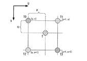
図19はバイリニアフィルタリングの概念を示す図である。同図中、Tはテクスチャ座標(U,V)が指す位置であり、pはUの小数部、qはVの小数部であり、0≦p<1、0≦q<1である。T0,T1,T2,T3は、Tの近傍4点の2次元格子上のテクスチャデータであり、Tの整数部を(u,v)とすると、T0の座標は(u,v)、T1の座標は(u+1,v)、T2の座標は(u,v+1)、T3の座標は(u+1,v+1)である。 FIG. 19 is a diagram showing the concept of bilinear filtering. In the figure, T is a position indicated by the texture coordinates (U, V), p is a decimal part of U, q is a decimal part of V, and 0 ≦ p <1 and 0 ≦ q <1. T0, T1, T2, and T3 are texture data on a two-dimensional lattice of four points in the vicinity of T. If the integer part of T is (u, v), the coordinates of T0 are (u, v), and T1 The coordinates are (u + 1, v), the coordinates of T2 are (u, v + 1), and the coordinates of T3 are (u + 1, v + 1).
バイリニアフィルタリングの計算式は、
T=(1−p)×(1−q)×T0+p×(1−q)×T1
+(1−p)×q×T2+p×q×T3
のようになり、T0,T1,T2,T3のRGB値についてそれぞれ計算する。
The bilinear filtering formula is
T = (1-p) * (1-q) * T0 + p * (1-q) * T1
+ (1-p) × q × T2 + p × q × T3
Thus, the RGB values of T0, T1, T2, and T3 are respectively calculated.
このように、バイリニアフィルタリングは、1個のテクスチャを生成するのに、4点のテクスチャデータを必要とする。LSIでテクスチャマッピングを行う際、テクスチャを内部メモリに格納してから参照するが、バイリニアフィルタリングを行う際には、1個のテクスチャを生成するのに内部メモリを4回参照する必要があり、処理が低速になる。 Thus, bilinear filtering requires four points of texture data to generate one texture. When texture mapping is performed by LSI, the texture is stored after being stored in the internal memory, but when bilinear filtering is performed, it is necessary to refer to the internal memory four times to generate one texture. Becomes slow.
従来、バイリニアフィルタリングを高速に処理するため、テクスチャを2次元格子上の座標(2m,2n)、(2m+1,2n)、(2m,2n+1)、(2m+1,2n+1)(m、nは整数)毎に分類し、この分類種に対応させて、テクスチャデータを4個のメモリに個別に格納し、バイリニアフィルタリングを行う際には、これら4個のメモリから同時にテクスチャデータを読み出す方法が提案されている(例えば、特許文献1参照)。
上述した従来の方法によると、テクスチャデータを4種類に分類して、それぞれ対応したメモリに格納する必要があるため、例えば、データバスを介して、複数ピクセルのテクスチャデータを同時にメモリまで転送できる場合において、転送動作を最速には実行できないという問題がある。 According to the conventional method described above, texture data needs to be classified into four types and stored in corresponding memories. For example, texture data of a plurality of pixels can be transferred to the memory simultaneously via a data bus. However, there is a problem that the transfer operation cannot be executed at the fastest speed.
例えば、テクスチャマッピング装置が16ビット(/pixel)と32ビット(/pixel)のテクスチャデータを扱う場合、内部メモリの各アドレスで記憶するデータのビット数は、通常、32ビットである。そして、内部メモリまでテクスチャデータを転送するデータバスのビット数が32であれば、16ビットのテクスチャデータは一度に2ピクセル分転送することができる。しかしながら、上述の従来の方法によると、この2ピクセル分のテクスチャデータは別々のメモリに格納する必要があるため、メモリにリード・モディファイ・ライトの処理が入ってしまい、これにより、最速で転送することができず、データバスの転送速度が低速になってしまう。 For example, when the texture mapping apparatus handles 16-bit (/ pixel) and 32-bit (/ pixel) texture data, the number of bits of data stored at each address of the internal memory is usually 32 bits. If the number of bits of the data bus for transferring texture data to the internal memory is 32, 16-bit texture data can be transferred for two pixels at a time. However, according to the above-described conventional method, it is necessary to store the texture data for the two pixels in different memories, so that the read / modify / write process is performed in the memory, and thus the transfer is performed at the highest speed. The data bus transfer speed becomes low.
また、従来の方法によれば、バイリニアフィルタリングを行う際、常に4個のメモリからテクスチャデータを読み出すため、メモリ部の消費電力が高くなるといった問題もある。 In addition, according to the conventional method, when bilinear filtering is performed, texture data is always read from four memories, so that there is a problem that the power consumption of the memory unit increases.
前記の問題に鑑み、本発明は、バイリニアフィルタリングを行うテクスチャ処理装置において、テクスチャデータをテクスチャメモリに高速に転送可能にし、バイリニアフィルタリング処理を高速に実行可能にすることを課題とする。 In view of the above problems, an object of the present invention is to enable texture data to be transferred to a texture memory at high speed and perform bilinear filtering processing at high speed in a texture processing apparatus that performs bilinear filtering.
前記の課題を解決するために、本発明は、テクスチャ処理装置として、テクスチャデータを格納するための第1、第2、第3および第4のテクスチャメモリと、与えられたテクスチャデータを前記第1〜第4のテクスチャメモリに書き込む制御を行うメモリ書き込み部と、テクスチャ座標の近傍の4点のテクスチャデータを前記第1〜第4のテクスチャメモリから読み出す制御を行うメモリ読み出し部と、前記メモリ読み出し部によって前記第1〜第4のテクスチャメモリから読み出された4点のテクスチャデータを用いて、バイリニアフィルタリング演算を行うバイリニアフィルタリング演算部とを備え、前記メモリ書き込み部は、1回の書き込み動作において、1度に転送可能でありかつ1個のアドレスに書き込み可能な個数のテクスチャデータを共通に前記第1〜第4のテクスチャメモリのうちのいずれか1つに対して書き込み、かつ、前記第1〜第4のテクスチャメモリへのデータ書き込みを、書き込むテクスチャデータのV座標が偶数のときは第1、第2、第3、第4の順に行う一方、奇数のときは第3、第4、第1、第2の順に行うものである。 In order to solve the above-mentioned problems, the present invention provides a texture processing apparatus that includes first, second, third, and fourth texture memories for storing texture data, and the given texture data as the first texture data. A memory writing unit for controlling writing to the fourth texture memory, a memory reading unit for controlling reading of four texture data in the vicinity of texture coordinates from the first to fourth texture memories, and the memory reading unit. A bilinear filtering operation unit that performs bilinear filtering using the four texture data read from the first to fourth texture memories, and the memory writing unit in one writing operation, The number of textures that can be transferred at one time and can be written to one address Write data to any one of the first to fourth texture memories in common and write data to the first to fourth texture memories, and the V coordinate of the texture data to be written is an even number In this case, the processing is performed in the order of the first, second, third, and fourth, while in the case of an odd number, the processing is performed in the order of the third, fourth, first, and second.
本発明によると、1回の書き込み動作において、1度に転送可能でありかつ1個のアドレスに書き込み可能な個数のテクスチャデータが、共通に、第1〜第4のテクスチャメモリのうちのいずれか1つに対して書き込まれる。このため、テクスチャデータの転送途中において余分な処理が不要となり、データバスの転送能力を活かした速度でデータ書き込みが実行できる。しかも、第1〜第4のテクスチャメモリへのデータ書き込みは、テクスチャデータのV座標が偶数のときは第1、第2、第3、第4の順に行われ、奇数のときは第3、第4、第1、第2の順に行われる。このため、U座標が同一でV座標が「1」違いのテクスチャデータは、必ず、異なるテクスチャメモリに格納される。これにより、バイリニアフィルタリング処理の際に、必要な4点のテクスチャデータを、一度に読み出すことができる。 According to the present invention, in one write operation, the number of texture data that can be transferred at one time and can be written to one address is one of the first to fourth texture memories. Written to one. For this reason, no extra processing is required during the transfer of texture data, and data can be written at a speed that utilizes the transfer capability of the data bus. In addition, data writing to the first to fourth texture memories is performed in the order of the first, second, third, and fourth when the V coordinate of the texture data is an even number, and the third and second when the texture data is an odd number. 4, first, second order. For this reason, texture data having the same U coordinate and a different V coordinate of “1” is always stored in different texture memories. As a result, necessary four points of texture data can be read at a time in the bilinear filtering process.
そして、前記本発明に係るテクスチャ処理装置におけるメモリ読み出し部は、データ読み出しの際に、前記第1〜第4のテクスチャメモリのうちアクセスが不要のテクスチャメモリに対し、チップイネーブルをディスエーブルにする、または、クロック入力を停止するのが好ましい。これにより、テクスチャ処理装置の消費電力を下げることができる。 The memory reading unit in the texture processing apparatus according to the present invention disables chip enable for a texture memory that does not require access among the first to fourth texture memories when reading data. Alternatively, it is preferable to stop the clock input. Thereby, the power consumption of the texture processing apparatus can be reduced.
また、前記本発明に係るテクスチャ処理装置におけるメモリ書き込み部は、与えられたテクスチャデータ群の先頭V座標が偶数か奇数かを示すVラインモードを受け、このVラインモードに応じて、各テクスチャデータのV座標が偶数か奇数かを判定するのが好ましい。 Further, the memory writing unit in the texture processing apparatus according to the present invention receives a V line mode indicating whether the leading V coordinate of the given texture data group is an even number or an odd number, and each texture data according to the V line mode. It is preferable to determine whether the V coordinate is even or odd.
さらに、前記メモリ書き込み部は、データ書き込みの開始アドレスが、設定可能に構成されているのが好ましい。または、前記メモリ書き込み部は、与えられたテクスチャデータを、指示されたシフト値だけシフトして、前記第1〜第4のテクスチャメモリに書き込むのが好ましい。 Furthermore, it is preferable that the memory writing unit is configured to be able to set a data writing start address. Alternatively, it is preferable that the memory writing unit shifts the given texture data by an instructed shift value and writes it to the first to fourth texture memories.
また、前記本発明に係るテクスチャ処理装置は、第1のテクスチャデータ群を格納した状態の前記第1〜第4のテクスチャメモリに、次に用いる第2のテクスチャデータ群を書き込む際に、前記第1〜第4のテクスチャメモリ内において、前記第1のテクスチャデータ群のV座標最大のテクスチャデータを、前記第2のテクスチャデータ群のV座標最小のテクスチャデータを格納する位置に移動させるメモリデータ移動制御部を備えているのが好ましい。 The texture processing apparatus according to the present invention writes the second texture data group to be used next into the first to fourth texture memories in a state where the first texture data group is stored. Memory data movement for moving the texture data having the maximum V coordinate of the first texture data group to a position storing the texture data having the minimum V coordinate of the second texture data group in the first to fourth texture memories. It is preferable to include a control unit.
また、前記本発明に係るテクスチャ処理装置において、前記メモリ書き込み部は、第1のテクスチャデータ群を格納した状態の前記第1〜第4のテクスチャメモリに、次に用いる第2のテクスチャデータ群を書き込む際に、前記第1のテクスチャデータ群のV座標最大のテクスチャデータに続けて、前記第2のテクスチャデータ群のうちV座標最小のテクスチャデータを除くテクスチャデータを書き込むものとし、前記メモリ読み出し部は、前記第2のテクスチャデータ群のテクスチャデータの読み出しを、前記第1のテクスチャデータ群のV座標最大のテクスチャデータが格納された位置を基準にして行うものとするのが好ましい。 Further, in the texture processing device according to the present invention, the memory writing unit stores a second texture data group to be used next in the first to fourth texture memories in a state where the first texture data group is stored. When writing, texture data excluding texture data with the smallest V coordinate in the second texture data group is written following the texture data with the largest V coordinate in the first texture data group, and the memory reading unit It is preferable that the texture data of the second texture data group is read with reference to the position where the texture data having the maximum V coordinate of the first texture data group is stored.
また、前記本発明に係るテクスチャ処理装置は、テクスチャデータの転送を、1ピクセル当たりのテクスチャデータが16ビットのときは2個ずつ行い、32ビットのときは1個ずつ行うものとするのが好ましい。 In the texture processing apparatus according to the present invention, it is preferable that the texture data is transferred two by one when the texture data per pixel is 16 bits, and one by one when the texture data is 32 bits. .
本発明によると、データバスを介して複数ピクセルのテクスチャデータを一度に転送できる場合に、データバスの転送能力を活かした速度で、テクスチャメモリに書き込むことができる。また、バイリニアフィルタリング処理の際も、必要な4個のテクスチャデータをテクスチャメモリから一度に読み出すことができる。したがって、テクスチャデータの転送を高速に実行できるとともに、バイリニアフィルタリング処理を高速に実行することができる。 According to the present invention, when texture data of a plurality of pixels can be transferred at a time via the data bus, the texture memory can be written at a speed utilizing the transfer capability of the data bus. Also, in the case of bilinear filtering processing, necessary four texture data can be read from the texture memory at a time. Therefore, texture data can be transferred at high speed, and bilinear filtering processing can be executed at high speed.
以下、本発明の実施の形態について、図面を参照して説明する。 Embodiments of the present invention will be described below with reference to the drawings.
(第1の実施形態)
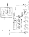
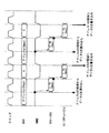
図1は本発明の第1の実施形態に係るテクスチャ処理装置の構成を示すブロック図である。図1において、第1、第2、第3および第4のテクスチャメモリ1a,1b,1c,1dは、テクスチャデータを格納するためのメモリであり、ここではそれぞれ32ビット×256ワードで構成されているものとする。また当該装置は、32ビットのデータが一度に転送可能なように構成されている。テクスチャメモリ1a〜1dは、クロックの立ち上がりエッジにおいてライトイネーブルやアドレス、データを取り込む。
(First embodiment)
FIG. 1 is a block diagram showing the configuration of the texture processing apparatus according to the first embodiment of the present invention. In FIG. 1, first, second, third, and
メモリ書き込み部2は、外部記憶手段等からロードされたテクスチャデータをテクスチャメモリ1a〜1dに対して書き込む制御を行うものであり、書き込みデータDI、書き込みアドレスWADa,WADb,WADc,WADd、およびライトイネーブルNWEa,NWEb,NWEc,NWEdを出力する。ここでは、与えられるテクスチャデータおよび書き込みデータDIは32ビット、書き込みアドレスWADa〜WADdは8ビットとする。またライトイネーブルNWEa〜NWEdは、“0”が書き込み状態を示し、“1”が読み出し状態を示すものとする。
The
メモリ読み出し部3は、与えられたテクスチャ座標(すでに整数に丸められたもの)に基づいて、テクスチャメモリ1a〜1dからバイリニアフィルタリングに必要なテクスチャデータを読み出す制御を行うものであり、読み出しアドレスRADa,RADb,RADc,RADd、およびチップイネーブルNCEa,NCEb,NCEc,NCEdを出力する。ここでは、読み出しアドレスRADa〜RADdは8ビットとする。またチップイネーブルNCEa〜NCEdは、“0”がメモリ1a〜1dを動作状態にし、“1”がメモリ1a〜1dを停止状態にするものとする。メモリ1a〜1dを停止状態にすることによって消費電力を抑えることができる。
The
セレクタ4a,4b,4c,4dは、テクスチャメモリ1a〜1dに対応してそれぞれ設けられている。各セレクタ4a〜4dは、テクスチャデータがテクスチャメモリ1a〜1dに書き込まれる期間は、メモリ書き込み部2から出力された書き込みアドレスWADa〜WADdを選択する一方、バイリニアフィルタリング演算処理期間は、メモリ読み出し部3から出力された読み出しアドレスRADa〜RADdを選択し、メモリアドレスADa,ADb,ADc,ADdとして、それぞれ出力する。
The
テクスチャ選択部5は、テクスチャメモリ1a〜1dから読み出されたデータDOa,DOb,DOc,DOdから、図19に示すような、バイリニアフィルタリング演算処理において必要になる4点のテクスチャデータT0〜T3を選択し出力する。バイリニアフィルタリング演算部6は、テクスチャ選択部5から選択出力された4点のテクスチャデータT0〜T3を用いてバイリニアフィルタリング演算を行い、バイリニアフィルタリングデータを出力する。このバイリニアフィルタリングデータは、図示しないフレームメモリの描画座標(X,Y)に対応する領域に書き込まれ、フレームメモリ上の図形データはディスプレイ等の表示装置で表示される。
The
以下、メモリ書き込み部2の構成および動作について、詳細に説明する。
Hereinafter, the configuration and operation of the
図2は図1におけるメモリ書き込み部2の内部構成を示す図である。図2において、制御用カウンタ7は、書き込みカウント値wcntを生成するものであり、加算器8、セレクタ9およびレジスタ10によって構成されている。加算器8はレジスタ10の値に“1”を加算する。セレクタ9は起動信号が“0”のときは加算器8の演算結果を選択する一方、起動信号が“1”のときは“0”を選択する。レジスタ10はセレクタ9の出力を記憶する10ビットのフリップフロップであり、レジスタ10の値が書き込みカウント値wcntとなる。
FIG. 2 is a diagram showing an internal configuration of the
ここで、『wcnt[9:0]』のようにデータ名の後に付した[]はそのデータのビット位置を示している。すなわち、[i:j]はiビット目からjビット目までの連続した(i−j+1)ビットを指す。例えば、先のwcnt[9:0]は、データwcntの9ビット目から0ビット目までの連続した10ビットを意味する。また、[i]はそのデータのiビット目の1ビットを指し、例えば、wcnt[0]はデータwcntの0ビット目を、wcnt[1]はデータwcntの1ビット目を意味する。 Here, [] attached after the data name such as “wcnt [9: 0]” indicates the bit position of the data. That is, [i: j] indicates consecutive (i−j + 1) bits from the i-th bit to the j-th bit. For example, the previous wcnt [9: 0] means 10 consecutive bits from the 9th bit to the 0th bit of the data wcnt. [I] indicates the first bit of the i-th bit of the data. For example, wcnt [0] indicates the 0th bit of the data wcnt, and wcnt [1] indicates the first bit of the data wcnt.
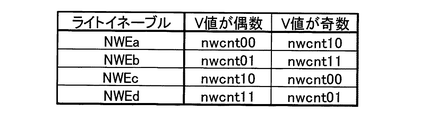
論理回路19aはwcnt[0]とwcnt[1]との論理和をとり、データnwcnt00として出力する。データnwcnt00は、wcnt[1:0]=00(2進数)のときのみ“0”になる。同様に、論理回路19bはwcnt[0]の論理否定とwcnt[1]との論理和をとり、データnwcnt01として出力する。データnwcnt01は、wcnt[1:0]=01(2進数)のときのみ“0”になる。論理回路19cはwcnt[0]とwcnt[1]の論理否定との論理和をとり、データnwcnt10として出力する。データnwcnt10は、wcnt[1:0]=10(2進数)のときのみ“0”になる。論理回路19dはwcnt[0]とwcnt[1]との論理積を論理否定し、データnwcnt11として出力する。データnwcnt11は、wcnt[1:0]=11(2進数)のときのみ“0”になる。
The
ライトイネーブル生成部11は、テクスチャデータのビット数(1ピクセル当たり)と横幅、および書き込みカウント値wcnt[9:0]を基にして、データnwcnt00,nwcnt01,nwcnt10,nwcnt11のいずれかを、ライトイネーブルNWEa,NWEb,NWEc,NWEdとしてそれぞれ選択する。図3および図4はライトイネーブルNWEa〜NWEdを選択するための条件の例を示す。ライトイネーブル生成部11から出力されたライトイネーブルNWEa〜NWEdはレジスタ12〜15にそれぞれ格納され、決定される。
Based on the number of bits (per pixel) and the width of the texture data, and the write count value wcnt [9: 0], the write enable
ここで、書き込むテクスチャデータのV座標が偶数のときは、テクスチャメモリ1a→1b→1c→1d→1a→・・・の順に書き込みを行い、奇数のときは、テクスチャメモリ1c→1d→1a→1b→1c→・・・の順に書き込みを行うように、ライトイネーブルNWEa〜NWEdが生成される。
Here, when the V coordinate of the texture data to be written is an even number, the
すなわち、図3に示すような条件によって、書き込むテクスチャデータのV座標が偶数か奇数かを判定する。例えば、テクスチャのビット数が16(bit/pixel)であり、横幅が8(pixel)のとき、転送可能なデータは32ビットであるため、1回のメモリ書き込みによって2ピクセルのテクスチャデータを書き込むことができ、8ピクセルのテクスチャデータをメモリに格納するために、4回のメモリ書き込みを行うことになる。すなわち、4回メモリに書き込む毎にV座標の偶数と奇数が切り替わることになり、wcnt[2]=0のときはV座標が偶数、wcnt[2]=1のときはV座標が奇数となる。 That is, it is determined whether the V coordinate of the texture data to be written is an even number or an odd number according to the conditions shown in FIG. For example, when the number of texture bits is 16 (bit / pixel) and the width is 8 (pixel), the transferable data is 32 bits, so 2 pixels of texture data is written by one memory write. In order to store the texture data of 8 pixels in the memory, the memory is written four times. That is, every time data is written to the memory four times, the even and odd V coordinates are switched. When wcnt [2] = 0, the V coordinate is even, and when wcnt [2] = 1, the V coordinate is odd. .
そして、図4に示すように、V座標が偶数か奇数かによって、ライトイネーブルNWEa〜NWEdを切り替える。 As shown in FIG. 4, the write enable NWEa to NWEd is switched depending on whether the V coordinate is an even number or an odd number.
レジスタ16は8ビットのフリップフロップであり、wcnt[9:2]すなわち書き込みカウント値の上位8ビットを記憶する。レジスタ16の値は書き込みアドレスWADa〜WADdの共通データとなる。書き込みアドレスWADa〜WADdは、wcnt[9:2]の値を用いているため、メモリ書き込みを4回行う毎に「1」増加する。レジスタ17は32ビットのフリップフロップであり、与えられたテクスチャデータを記憶する。レジスタ17の値は書き込みデータDIとして出力される。書き込み終了判定部18は書き込みカウント値wcnt[9:0]をモニターし、メモリ書き込みの回数が処理に必要な所定数に達したとき、メモリ書き込み処理を終了させる。
The
図5はメモリ書き込み処理を示すタイミングチャートである。図5では、テクスチャデータのビット数が16(bit/pixel)、横幅が8(pixel)の場合を例にとって示している。図5に示すように、書き込みアドレスWADa〜WADdが“0”の期間は、書き込むテクスチャデータのV座標が偶数であり、ライトイネーブルNWEa〜NWEdはNWEa→NWEb→NWEc→NWEdの順にアサートされる。これにより、第1〜第4のテクスチャメモリ1a〜1dへの書き込みは、第1(1a)、第2(1b)、第3(1c)、第4(1d)の順に行われる。一方、書き込みアドレスWADa〜WADdが“1”の期間は、書き込むテクスチャデータのV座標が奇数であり、ライトイネーブルNWEa〜NWEdはNWEc→NWEd→NWEa→NWEbの順にアサートされる。これにより、第1〜第4のテクスチャメモリ1a〜1dへの書き込みは、第3(1c)、第4(1d)、第1(1a)、第2(1b)の順に行われる。
FIG. 5 is a timing chart showing the memory writing process. FIG. 5 shows an example in which the number of bits of texture data is 16 (bit / pixel) and the horizontal width is 8 (pixel). As shown in FIG. 5, during the period when the write addresses WADA to WADd are “0”, the V coordinate of the texture data to be written is an even number, and the write enable NWEa to NWEd are asserted in the order of NWEa → NWEb → NWEc → NWEd. As a result, writing to the first to
このように、1回の書き込み動作において、1度に転送可能な1個または複数個のテクスチャデータが、共通に、第1〜第4のテクスチャメモリ1a〜1dのうちのいずれか1つに対して書き込まれるため、連続サイクルで、テクスチャデータをメモリに高速に書き込むことが可能である。
As described above, in one writing operation, one or a plurality of texture data that can be transferred at one time is commonly used for any one of the first to
次に、メモリ読み出し部3の構成および動作について、詳細に説明する。
Next, the configuration and operation of the
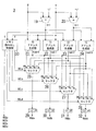
図6は図1におけるメモリ読み出し部3の内部構成を示す図である。図6において、加算器19,20は、与えられたU座標およびV座標に「1」をそれぞれ加算する。そして、T0アドレス生成部21は、座標(U,V)に対応するテクスチャデータのメモリアドレスradr0を生成出力する。同様に、T1アドレス生成部22は座標(U+1,V)に対応するテクスチャデータのメモリアドレスradr1を、T2アドレス生成部23は座標(U,V+1)に対応するテクスチャデータのメモリアドレスradr2を、そしてT3アドレス生成部24は座標(U+1,V+1)に対応するテクスチャデータのメモリアドレスradr3を、それぞれ生成出力する。メモリアドレスradr0〜radr3はそれぞれ8ビットである。
FIG. 6 is a diagram showing an internal configuration of the
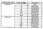
図7はT0アドレス生成部21におけるメモリアドレス生成内容を示す。同図中、例えば{V[5:0],U[4:3]}とあるのは、座標値Vの5ビット目から0ビット目までの連続した6ビットと、座標値Uの4ビット目から3ビット目までの連続した2ビットを連結した8ビットの値を示す。T1アドレス生成部22、T2アドレス生成部23およびT3アドレス生成部24も、同様にしてメモリアドレスを生成する。
FIG. 7 shows the contents of memory address generation in the T0
セレクタ25は、2ビットのセレクト信号SELaに応じて、メモリアドレスradr0〜radr3のいずれかを選択する。同様に、セレクタ26,27,28はそれぞれ、2ビットのセレクト信号SELb,SELc,SELdに応じて、メモリアドレスradr0〜radr3のいずれかを選択する。セレクタ25〜28は、セレクト信号SELa〜SELdが、“00”(2進数)のときはradr0を選択し、“01”(2進数)のときはradr1を選択し、“10”(2進数)のときはradr2を選択し、“11”(2進数)のときはradr3を選択する。レジスタ29,30,31,32はセレクタ25〜28で選択されたアドレスを記憶し、読み出しアドレスRADa〜RADdとしてそれぞれ出力する。
The
メモリ読み出し制御部33は、座標(U,V)を基にして、上述したセレクト信号SELa〜SELdを生成するとともに、各テクスチャメモリ1a〜1dのチップイネーブルNCEa〜NCEdを生成する。図8はメモリ読み出し制御部33におけるセレクト信号SELa〜SELdの生成内容を示す。同図中、V[0],U[2:0],SELa〜SELdはそれぞれ2進数で表記している。なお、図8においてハッチを付した部分は、そのときのデータ読み出しにおいてアクセスする必要がないメモリに係るものであり、一応“00”(2進数)と図示しているが、どのような値でもよい。
The memory read
また、データ読み出しの際に、アクセスが不要のテクスチャメモリに対しては、チップイネーブルをディスエーブルにするのが好ましい。図9はメモリ読み出し制御部33におけるチップイネーブルNCEa〜NCEdの生成内容を示す。同図中、ハッチを付した部分は、図8のハッチを付した部分と同一条件になっており、この場合、メモリに対してアクセスする必要がないため、チップイネーブルを“1”にしてディスエーブル状態にする。これにより、メモリ動作を止めることができ、消費電力を下げることができる。なお、アクセスが不要のテクスチャメモリに対しては、チップイネーブルをディスエーブルにする代わりに、またはこれとともに、クロック入力を停止してもよい。
In addition, it is preferable to disable chip enable for a texture memory that does not require access when reading data. FIG. 9 shows the generation contents of chip enables NCEa to NCEd in the memory read
そして、テクスチャ選択部5は、図10に示すような内容に従って、テクスチャメモリ1a〜1dから読み出されたデータDOa〜DOdから、バイリニアフィルタリング演算に必要な4点のテクスチャデータT0〜T3を選択する。なお、テクスチャデータのビット数が16(bit/pixel)の場合、32ビットのデータDOa〜DOdのうちの16ビットを選択するが、テクスチャデータT0〜T3としては、バイリニアフィルタリング演算部4において演算可能なように、R,G,Bの各値のビット数を拡張して出力する。
Then, the
図11は本実施形態におけるテクスチャデータの書き込みおよび読み出しを概念的に示す図であり、(a)はビット数が16の場合、(b)はビット数が32の場合である。同図中、a〜dの記号は、それぞれ、第1〜第4のテクスチャメモリ1a〜1dにテクスチャデータが書き込まれることを示している。図11(a)に示すように、テクスチャデータが16ビットの場合、各テクスチャデータは、一度に転送できる2個単位で、各テクスチャメモリ1a〜1dに書き込まれる。すなわち、テクスチャデータを高速に転送することができる。また、破線矩形枠A,B,Cで示すとおり、必要な4個のテクスチャデータは、複数のテクスチャメモリから、同一サイクルで読み出すことができる。なお、例えば矩形枠Aの場合、データ読み出しは第1および第3のテクスチャメモリ1a,1cから行えばよく、第2および第4のテクスチャメモリ1b,1dのアクセスは不要であるので、上述したとおり、チップイネーブルNCEb,NCEdがディセーブルにされる。
FIGS. 11A and 11B are diagrams conceptually showing writing and reading of texture data in this embodiment. FIG. 11A shows a case where the number of bits is 16, and FIG. 11B shows a case where the number of bits is 32. In the figure, symbols a to d indicate that texture data is written in the first to
以上のように本実施形態によると、テクスチャデータをテクスチャメモリに転送する際、常に、連続サイクルで書き込みを行うことができるので、テクスチャデータを高速に転送することができる。また、バイリニアフィルタリング処理に必要な4点のテクスチャデータを、同一サイクルで、読み出すことができるので、処理を高速に実行することができる。また、データ読み出しの際に、アクセスが必要のテクスチャメモリに対して、チップイネーブルをディスエーブルにしたり、クロック入力を停止することによって、装置の消費電力を下げることができる。 As described above, according to this embodiment, when texture data is transferred to the texture memory, writing can always be performed in a continuous cycle, so that the texture data can be transferred at high speed. In addition, since the four points of texture data necessary for the bilinear filtering process can be read out in the same cycle, the process can be executed at high speed. In addition, when data is read, the power consumption of the apparatus can be reduced by disabling chip enable or stopping clock input to the texture memory that needs to be accessed.
なお、本実施形態では、テクスチャメモリの各アドレスには32ビットのデータが書き込み可能であり、一度に転送可能なデータも32ビットであり、テクスチャデータは16ビットと32ビットとの2種類があるものとしたが、本発明はこれに限られるものではなく、発明の主旨を逸脱しない範囲で様々な態様のものが考えられる。例えば、一度に64ビットのデータが転送可能なように構成されている場合は、テクスチャデータが16ビットのときは、4個のテクスチャデータを転送し、2個ずつ、例えば第1および第2のテクスチャメモリに同時に書き込むようにし、テクスチャデータが32ビットのときは、2個のテクスチャデータを転送し、1個ずつ、第1および第2のテクスチャメモリに同時に書き込むようにしてもよい。すなわち、1度に転送可能でありかつ1個のアドレスに書き込み可能な個数のテクスチャデータを、いずれか1つのテクスチャメモリに共通に書き込むようにすることによって、データバスの転送能力を活かした速度で、データ書き込みが実行できる。 In this embodiment, 32-bit data can be written to each address of the texture memory, data that can be transferred at a time is 32 bits, and there are two types of texture data, 16 bits and 32 bits. However, the present invention is not limited to this, and various forms can be considered without departing from the gist of the invention. For example, when it is configured so that 64-bit data can be transferred at a time, when the texture data is 16 bits, four texture data are transferred, and two each, for example, the first and second The texture memory may be simultaneously written, and when the texture data is 32 bits, two texture data may be transferred and written one by one to the first and second texture memories. In other words, the number of texture data that can be transferred at one time and that can be written to one address is written in common to any one of the texture memories at a speed that utilizes the transfer capability of the data bus. Data writing can be executed.
(第2の実施形態)
本発明の第2の実施形態に係るテクスチャ処理装置の構成は、基本的には図1に示すとおりであるが、第1の実施形態とは、メモリ書き込み部2Aの構成が異なっている。図12は本実施形態におけるメモリ書き込み部2Aの構成を示すブロック図である。同図中、第1の実施形態で示した図2と共通の構成要素については図2と同一の符号を付しており、ここではその詳細な説明を省略する。
(Second Embodiment)
The configuration of the texture processing apparatus according to the second embodiment of the present invention is basically as shown in FIG. 1, but the configuration of the
ライトイネーブル生成部34は、書き込みカウント値wcntおよびデータnwcnt00,nwcnt01,nwcnt10,nwcnt11に加えて、VラインモードVMを受ける。そして、テクスチャデータのビット数と横幅、書き込みカウント値wcnt[9:0]、およびVラインモードVMを基にして、データnwcnt00,nwcnt01,nwcnt10,nwcnt11のいずれかを、ライトイネーブルNWEa,NWEb,NWEc,NWEdとしてそれぞれ選択する。
The write enable
ここで、VラインモードVMとは、与えられたテクスチャデータ群の先頭V座標が偶数か奇数かを示す信号であり、“0”のときは先頭V座標が偶数、“1”のときは先頭V座標が奇数であることを示す。 Here, the V line mode VM is a signal indicating whether the leading V coordinate of the given texture data group is an even number or an odd number. Indicates that the V coordinate is an odd number.
VラインモードVMが“0”のとき、すなわち、書き込むテクスチャデータ群のV座標が偶数から始まる場合は、各テクスチャデータのV座標が偶数か奇数か判定する条件は、第1の実施形態で図3に示したものと同様である。一方、Vラインモードが“1”のとき、すなわち、書き込むテクスチャデータ群のV座標が奇数から始まる場合は、各テクスチャデータのV座標が偶数か奇数か判定する条件は、図13のようになる。そして第1の実施形態と同様に、図4に示すように、V座標が偶数か奇数かによって、ライトイネーブルNWEa〜NWEdを切り替える。 When the V line mode VM is “0”, that is, when the V coordinate of the texture data group to be written starts from an even number, the conditions for determining whether the V coordinate of each texture data is an even number or an odd number are the same as those in the first embodiment. This is the same as that shown in FIG. On the other hand, when the V line mode is “1”, that is, when the V coordinate of the texture data group to be written starts from an odd number, the condition for determining whether the V coordinate of each texture data is an even number or an odd number is as shown in FIG. . As in the first embodiment, as shown in FIG. 4, the write enable NWEa to NWEd is switched depending on whether the V coordinate is an even number or an odd number.
レジスタ39は、起動信号を1サイクルディレイさせるためのフリップフロップである。書き込みアドレス生成部40は、書き込みアドレスWADa〜WADdを生成するものであり、加算器41、セレクタ42,43およびレジスタ44によって構成される。加算器41はレジスタ44の値に“1”を加算する。セレクタ42は、起動信号とレジスタ39の値との論理和をとった信号が、“0”のときは加算器41の演算結果を選択する一方、“1”のときは開始アドレスを選択する。この開始アドレスは、当該テクスチャ処理装置の外部から設定可能である。セレクタ43は、データnwcnt00が“0”のときはセレクタ42の出力を選択する一方、“1”のときはレジスタ44の値を選択する。レジスタ44はセレクタ43の出力を記憶する8ビットのフリップフロップである。
The
レジスタ44の値であるwadr[7:0]は、書き込みアドレスWADa〜WADdの共通データとなる。データnwcnt00は4サイクルに1回“0”になるので、レジスタ44の値は4サイクルに1回更新される。すなわち、書き込みアドレスWADa〜WADdはメモリ書き込みを4回行う毎に「1」増加する。 Wadr [7: 0], which is the value of the register 44, becomes common data for the write addresses WADa to WADd. Since the data nwcnt00 becomes “0” once every four cycles, the value of the register 44 is updated once every four cycles. That is, the write addresses WADa to WADd increase by “1” every time memory writing is performed four times.
レジスタ45は32ビットのフリップフロップであり、テクスチャデータload[31:0]をデータload1[31:0]として保持する。左シフター46は、レジスタ45に保持されたデータload1[31:0]と与えられたテクスチャデータload[31:0]とを連結した64ビットのデータを、指示されたシフト値に従って、左シフトする。このシフト値は、当該テクスチャ処理装置の外部から与えることができる。レジスタ47は32ビットのフリップフロップであり、左シフター46の出力の上位32ビットを記憶する。レジスタ47の値は書き込みデータDIとなる。
The
本実施形態によると、VラインモードVMに応じて、各テクスチャデータのV座標が偶数か奇数かを判定するので、与えられたテクスチャデータ群の先頭V座標が偶数であっても奇数であっても、第1の実施形態と同様のデータ書き込みを実現することができる。また、データ書き込みの開始アドレスが設定可能に構成されているので、与えられたテクスチャデータをテクスチャメモリの任意のアドレスに書き込むことができ、例えば、転送元のテクスチャデータを横1ラインずつ、テクスチャメモリの任意のアドレスに書き込むことができる。このため、第1の実施形態では転送元のテクスチャデータが必ず外部記憶手段の連続するアドレスに格納されている、という制約があるのに対して、本実施形態では、例えば、外部記憶手段上の大きなテクスチャデータの中のある矩形領域部分を切り出して、テクスチャメモリに転送する、といった動作が可能になる。 According to the present embodiment, whether the V coordinate of each texture data is an even number or an odd number is determined according to the V line mode VM, so even if the leading V coordinate of a given texture data group is an even number, it is an odd number. Also, data writing similar to that of the first embodiment can be realized. In addition, since the start address for data writing can be set, the given texture data can be written to any address in the texture memory. For example, the texture data of the transfer source can be written line by line in the texture memory. Can be written to any address. For this reason, in the first embodiment, there is a restriction that the texture data of the transfer source is always stored at consecutive addresses in the external storage unit, whereas in the present embodiment, for example, on the external storage unit It is possible to perform an operation such as cutting out a certain rectangular area portion in large texture data and transferring it to the texture memory.
また、転送中のテクスチャデータをシフトすることができるので、テクスチャデータの開始位置をワード境界上に置く必要がなく、さらに自由度の高いテクスチャデータの転送が可能になる。 Further, since the texture data being transferred can be shifted, it is not necessary to place the start position of the texture data on the word boundary, and the texture data can be transferred with a higher degree of freedom.
(第3の実施形態)
図14は本発明の第3の実施形態に係るテクスチャ処理装置の構成を示すブロック図である。同図中、図1と共通の構成要素には図1と同一の符号を付しており、ここではその詳細な説明を省略する。テクスチャメモリ1a〜1d、メモリ読み出し部3、テクスチャ選択部5およびバイリニアフィルタリング演算部6は第1の実施形態で説明したものと同様であり、メモリ書き込み部2Aは第2の実施形態で説明したものと同様である。
(Third embodiment)
FIG. 14 is a block diagram showing a configuration of a texture processing apparatus according to the third embodiment of the present invention. In the figure, components common to those in FIG. 1 are denoted by the same reference numerals as those in FIG. 1, and detailed description thereof is omitted here. The
メモリデータ移動制御部48は、前のバイリニアフィルタリング処理のときに第1〜第4のテクスチャメモリ1a〜1dに格納されたテクスチャデータ群のうちV座標最大のテクスチャデータを、第1〜第4のテクスチャメモリ1a〜1d内において、次のバイリニアフィルタリング処理のために用いるテクスチャデータ群のうちV座標最小(ここでは0)のテクスチャデータを格納する領域に、移動させる機能を有する。
The memory data
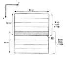
図15は外部記憶手段上のテクスチャデータを分割して内部のテクスチャメモリに転送してバイリニアフィルタリングを行う場合のデータ分割の例を示す概念図であり、8ピクセル×5ピクセルの領域でテクスチャを分割する場合を例にとっている。図15では、第1のテクスチャデータ群と第2のテクスチャデータ群とで、領域ARが重複している。すなわち、バイリニアフィルタリングのためにテクスチャデータを分割する際には、境界部分が1ライン重なるようにする。これは、テクスチャデータ群の境界部分についてバイリニアフィルタリングを行うには、隣接するテクスチャデータが必要になるためである。 FIG. 15 is a conceptual diagram showing an example of data division when the texture data on the external storage means is divided and transferred to the internal texture memory and bilinear filtering is performed, and the texture is divided into an area of 8 pixels × 5 pixels. Take this as an example. In FIG. 15, the area AR overlaps between the first texture data group and the second texture data group. That is, when the texture data is divided for bilinear filtering, the boundary portion is overlapped by one line. This is because in order to perform bilinear filtering on the boundary portion of the texture data group, adjacent texture data is required.
このため、第1のテクスチャメモリ群をテクスチャメモリ1a〜1dに格納し、バイリニアフィルタリング処理を行った後、第2のテクスチャメモリ群をテクスチャメモリ1a〜1dに格納する場合には、通常は、重複領域ARのテクスチャデータが、テクスチャメモリ1a〜1dに2度書きされることになる。
For this reason, when the second texture memory group is stored in the
これに対して本実施形態では、メモリデータ移動制御部48を設けることによって、重複領域ARの2度書きを回避し、外部記憶手段からのテクスチャデータの転送量を削減することができる。すなわち、メモリデータ移動制御部48が、第1のテクスチャメモリ群に対するバイリニアフィルタリング処理が終了した後、メモリデータ移動期間において、重複領域ARのテクスチャデータをテクスチャメモリ1a〜1d内において移動させる処理を行う。
On the other hand, in the present embodiment, by providing the memory data
メモリデータ移動制御部48は、データ移動処理用のメモリアドレスMADおよびライトイネーブルNMWEを出力し、セレクタ49、セレクタ50a〜50dおよびセレクタ52a〜52dを制御する。
The memory data
セレクタ49は、データ移動処理期間はライトイネーブルNMWEを選択し、それ以外の期間はライトイネーブルNWEa〜NWEdを選択し、ライトイネーブルNWEa’〜NWEd’として出力する。
The
セレクタ50a〜50dは、テクスチャデータをテクスチャメモリ1a〜1dに書き込む期間は書き込みアドレスWADa〜WADdを選択し、バイリニアフィルタリング演算処理期間は読み出しアドレスRADa〜RADdを選択し、データ移動処理期間はアドレスMADを選択し、メモリアドレスADa〜ADdとして出力する。
The
レジスタ51a〜51dは32ビットのフリップフロップであり、テクスチャメモリ1a〜1dから読み出されたデータDOa〜DOdを記憶する。セレクタ52a〜52dは、データ移動処理期間はレジスタ51a〜51dの出力を選択し、それ以外の期間は書き込みデータDIを選択し、書き込みデータDIa〜DIdとして出力する。
The registers 51a to 51d are 32-bit flip-flops and store data DOa to DOd read from the
図16はテクスチャメモリ1a〜1d内のデータ移動処理の例を示すタイミングチャートである。なお、4個のテクスチャメモリ1a〜1dそれぞれに対して、同時に処理が行われる。図16では、V座標最大すなわち重複領域のテクスチャデータが2個のアドレスa,bにわたって存在する場合を例にとって示している。
FIG. 16 is a timing chart showing an example of data movement processing in the
図16に示すように、メモリデータ移動制御部48は、アドレスMADとして「アドレスa」を2サイクル出力し、これに並行して、ライトイネーブルNMWEをメモリ読み出し状態(NMWE=“1”)で2サイクル出力し、テクスチャメモリ1a〜1dからアドレスaにおける各データを読み出し、レジスタ51a〜51dにそれぞれ格納する。
As shown in FIG. 16, the memory data
次のサイクルにおいて、アドレスMADとして“0”を1サイクル出力し、これに並行して、ライトイネーブルNMWEをメモリ書き込み状態(NMWE=“0”)で1サイクル出力し、テクスチャメモリ1a〜1dのアドレス0に対応する領域に、レジスタ51a〜51dに格納されたデータをそれぞれ書き込む。その後、「アドレスb」についても同様にしてデータを読み出し、テクスチャメモリ1a〜1dのアドレス1に対応する領域に、書き込む。
In the next cycle, “0” is output as the address MAD for one cycle, and in parallel with this, the write enable NMWE is output for one cycle in the memory write state (NMWE = “0”), and the addresses of the
このような動作によって、テクスチャメモリ内で、テクスチャデータ群同士の重複領域におけるテクスチャデータが、V座標最大となる領域からV座標が0となる領域に移動される。なお図16では、V座標最大のテクスチャデータが2個のアドレスに存在する場合について示したが、V座標最大のテクスチャデータは、1個のアドレスに存在する場合もあるし、3個以上のアドレスにわたって存在する場合もある。 By such an operation, the texture data in the overlapping region between the texture data groups is moved from the region where the V coordinate is maximum to the region where the V coordinate is 0 in the texture memory. Note that FIG. 16 shows the case where the texture data with the maximum V coordinate exists at two addresses, but the texture data with the maximum V coordinate may exist at one address, or three or more addresses. There may be over there.
テクスチャメモリ1a〜1d内で重複領域におけるテクスチャデータを移動した後は、次のテクスチャデータ群をテクスチャメモリ1a〜1dに書き込む際、重複領域のテクスチャデータを除いた分を、移動されたテクスチャデータの続きのアドレスからテクスチャメモリ1a〜1dに書き込めばよい。
After the texture data in the overlapping area is moved in the
以上のように本実施形態によると、外部記憶手段上のテクスチャデータを分割して内部のテクスチャメモリに転送してバイリニアフィルタリングを行う際に、重複領域のテクスチャデータを予めテクスチャメモリ内で移動しておくため、次のテクスチャデータ群の転送量を削減できるので、テクスチャデータの転送をより高速に行うことができる。 As described above, according to the present embodiment, when the texture data on the external storage means is divided and transferred to the internal texture memory and bilinear filtering is performed, the texture data in the overlapping region is moved in the texture memory in advance. Therefore, since the transfer amount of the next texture data group can be reduced, the texture data can be transferred at higher speed.
(第4の実施形態)
図17は本発明の第4の実施形態に係るテクスチャ処理装置の構成を示すブロック図である。同図中、図1と共通の構成要素には図1と同一の符号を付しており、ここではその詳細な説明を省略する。テクスチャメモリ1a〜1d、メモリ読み出し部3、セレクタ4a〜4d、テクスチャ選択部5およびバイリニアフィルタリング演算部6は第1の実施形態で説明したものと同様であり、メモリ書き込み部2Aは第2の実施形態で説明したものと同様である。
(Fourth embodiment)
FIG. 17 is a block diagram showing a configuration of a texture processing apparatus according to the fourth embodiment of the present invention. In the figure, components common to those in FIG. 1 are denoted by the same reference numerals as those in FIG. 1, and detailed description thereof is omitted here. The
本実施形態では、メモリ書き込み部2Aは、外部記憶手段上のテクスチャデータを分割してテクスチャメモリ1a〜1dに転送してバイリニアフィルタリングを行う際、すでにテクスチャメモリ1a〜1dに格納されたテクスチャデータのうちV座標最大のテクスチャデータが格納されたアドレスの続きに書き込み開始アドレスを設定し、次の分割されたテクスチャデータ群から重複領域のテクスチャデータを除いた分を、テクスチャメモリ1a〜1dに書き込む。
In the present embodiment, when the
なお、開始アドレスから順にテクスチャデータをテクスチャメモリに書き込む際、書き込みアドレスがテクスチャメモリの最大アドレスを超えた場合は、書き込みアドレスを0に戻し、続きのテクスチャデータを順に書き込む。ここでは、書き込みアドレス生成部40のレジスタ44は8ビットのフリップフロップであり、メモリアドレスを生成できる最低限のものである。このため、最大アドレスを越えたときは、書き込みアドレスは自動的に0に戻ることになる。
When writing texture data to the texture memory in order from the start address, if the write address exceeds the maximum address of the texture memory, the write address is returned to 0 and the subsequent texture data is written in order. Here, the register 44 of the write
ここで、図示していないCPUのような外部制御部が、次のような動作を行う。外部制御部は、書き込みアドレスを把握しており、その続きのアドレスを書き込み開始アドレスに設定する。これにより、V座標最大のテクスチャデータのアドレスが認識されたことになる。また外部制御部は、次のテクスチャデータ群について、重複領域の続きからデータを転送する。これにより、重複領域のテクスチャデータが次のテクスチャデータ群から除かれることになる。 Here, an external control unit such as a CPU (not shown) performs the following operation. The external control unit grasps the write address and sets the subsequent address as the write start address. As a result, the address of the texture data with the maximum V coordinate is recognized. Also, the external control unit transfers data from the continuation of the overlapping area for the next texture data group. As a result, the texture data of the overlapping region is excluded from the next texture data group.
図18は分割されたテクスチャデータ群が順にテクスチャメモリに格納される様子を示す。図18では、32ビットのテクスチャデータを横128ピクセル×縦8ピクセルの領域で分割した場合を例にとっており、4個のテクスチャメモリ1a〜1dのメモリ領域を総合して図示している。
FIG. 18 shows a state in which the divided texture data groups are sequentially stored in the texture memory. FIG. 18 shows an example in which 32-bit texture data is divided into an area of horizontal 128 pixels × vertical 8 pixels, and the memory areas of the four
図18(a)は第1のテクスチャデータ群がテクスチャメモリに格納された状態であり、Vaは第1のテクスチャデータ群のV座標である。図18(b)は第2のテクスチャデータ群がテクスチャメモリに格納された状態であり、Vbは第2のテクスチャデータ群のV座標である。第1のテクスチャデータ群との重複領域となるVa=7の領域は、そのままVb=0の領域として用い、Vb=0の領域に続いて、Vb=1〜7のテクスチャデータを格納する。ただし、Vb=0の領域はメモリアドレスの最大アドレスに存在するため、Vb=1以降のテクスチャデータは、アドレス0に戻って順に格納される。
FIG. 18A shows a state in which the first texture data group is stored in the texture memory, and Va is the V coordinate of the first texture data group. FIG. 18B shows a state in which the second texture data group is stored in the texture memory, and Vb is the V coordinate of the second texture data group. The area of Va = 7, which is the overlapping area with the first texture data group, is used as the area of Vb = 0 as it is, and the texture data of Vb = 1 to 7 is stored following the area of Vb = 0. However, since the region of Vb = 0 exists at the maximum address of the memory address, texture data after Vb = 1 is stored in order returning to
図18(c)は第3のテクスチャデータ群が格納された状態であり、Vcは第3のテクスチャデータ群のV座標である。第2のテクスチャデータ群との重複領域となるVb=7の領域は、そのままVc=0の領域として用い、Vc=0の領域に続いて、Vc=1〜7のテクスチャデータを格納する。ただし、Vc=1の領域はメモリアドレスの最大アドレスに存在するため、Vc=2以降のテクスチャデータは、アドレス0に戻って順に格納される。
FIG. 18C shows a state in which the third texture data group is stored, and Vc is the V coordinate of the third texture data group. The region of Vb = 7, which is the overlapping region with the second texture data group, is used as it is as the region of Vc = 0, and the texture data of Vc = 1 to 7 is stored following the region of Vc = 0. However, since the area of Vc = 1 exists at the maximum address of the memory address, the texture data after Vc = 2 is returned to
テクスチャ座標変換部53は、図18のように格納された各テクスチャデータがメモリ読み出し部3によって正しく読み出せるように、テクスチャ座標(U,V)を(U’,V’)に変換して出力する。すなわち、テクスチャ座標変換部53は、座標値Uはそのまま座標値U’として出力し、座標値Vはテクスチャメモリ1a〜1dに格納されているテクスチャデータのV座標0の領域の位置に応じて、座標値V’に変換する。これは、メモリ読み出し部3では、V座標0の領域がメモリアドレス0に存在することを前提にテクスチャ読み出しを行うからである。ここで、V座標0の領域の位置は、上述のCPUのような外部制御部が覚えておく。そして、外部からテクスチャ座標変換部53に対して、V座標0の領域の位置を設定する。
The texture coordinate
ここで、テクスチャメモリ1a〜1dに格納されているテクスチャデータのV座標0の領域の位置をVS、テクスチャデータ群の縦方向のピクセル長をTH、そしてTH−VSをVMとすると、座標値VのV’への変換は、
V<VSのとき V’=V+VS
V≧VSのとき V’=V−VM
とすればよい。図18(c)の場合を例にとると、VS=6、TH=8、VM=TH−VS=8−6=2となり、V=1のときは、V<VSなので、V’=V+VS=1+6=7となり、また、V=4のときは、V≧VSなので、V’=V−VM=4−2=2となる。このようにして、テクスチャデータの読み出しが正しく行えるように、テクスチャ座標の変換が行われる。
Here, assuming that the position of the V coordinate 0 area of the texture data stored in the
When V <VS V '= V + VS
When V ≧ VS V ′ = V−VM
And it is sufficient. Taking the case of FIG. 18C as an example, VS = 6, TH = 8, VM = TH-VS = 8-6 = 2, and when V = 1, since V <VS, V ′ = V + VS. = 1 + 6 = 7, and when V = 4, since V ≧ VS, V ′ = V−VM = 4-2 = 2. In this way, texture coordinates are converted so that the texture data can be read correctly.
以上のように本実施形態によると、テクスチャデータを分割してテクスチャメモリに転送してバイリニアフィルタリングを行う際、第3の実施形態のように、重複領域のテクスチャデータを予めテクスチャメモリ内で移動する必要がないため、データを移動させる回路を削減できるだけでなく、テクスチャメモリ内でデータを移動させる処理を省くことができるので、テクスチャデータの転送をさらに高速に実行することができる。 As described above, according to the present embodiment, when the texture data is divided and transferred to the texture memory and bilinear filtering is performed, the texture data in the overlapping region is moved in the texture memory in advance as in the third embodiment. Since it is not necessary, not only the circuit for moving the data can be reduced, but also the processing for moving the data in the texture memory can be omitted, so that the transfer of the texture data can be executed at a higher speed.
本発明では、テクスチャデータがテクスチャメモリに高速に転送され、バイリニアフィルタリング処理が高速に実行可能になるので、例えば、ゲーム機やカーナビゲーションにおいて、テクスチャマッピングをより高速に実現することができる。 In the present invention, the texture data is transferred to the texture memory at a high speed, and the bilinear filtering process can be executed at a high speed. For example, texture mapping can be realized at a higher speed in a game machine or a car navigation system.
1a 第1のテクスチャメモリ
1b 第2のテクスチャメモリ
1c 第3のテクスチャメモリ
1d 第4のテクスチャメモリ
2,2A メモリ書き込み部
3 メモリ読み出し部
6 バイリニアフィルタリング演算部
48 メモリデータ移動制御部
NCEa,NCEb,NCEc,NCEd チップイネーブル
DESCRIPTION OF
Claims (9)
与えられたテクスチャデータを、前記第1〜第4のテクスチャメモリに書き込む制御を行うメモリ書き込み部と、
テクスチャ座標の近傍の4点のテクスチャデータを、前記第1〜第4のテクスチャメモリから読み出す制御を行うメモリ読み出し部と、
前記メモリ読み出し部によって前記第1〜第4のテクスチャメモリから読み出された4点のテクスチャデータを用いて、バイリニアフィルタリング演算を行うバイリニアフィルタリング演算部とを備え、
前記メモリ書き込み部は、
1回の書き込み動作において、1度に転送可能でありかつ1個のアドレスに書き込み可能な個数のテクスチャデータを、共通に、前記第1〜第4のテクスチャメモリのうちのいずれか1つに対して、書き込み、かつ、
前記第1〜第4のテクスチャメモリへのデータ書き込みを、書き込むテクスチャデータのV座標が偶数のときは、第1、第2、第3、第4の順に行う一方、奇数のときは、第3、第4、第1、第2の順に、行うものである
ことを特徴とするテクスチャ処理装置。 First, second, third and fourth texture memories for storing texture data;
A memory writing unit that performs control to write the given texture data into the first to fourth texture memories;
A memory reading unit for performing control to read out four texture data in the vicinity of the texture coordinates from the first to fourth texture memories;
A bilinear filtering calculation unit that performs bilinear filtering calculation using the four points of texture data read from the first to fourth texture memories by the memory reading unit;
The memory writing unit
In one writing operation, the number of texture data that can be transferred at one time and that can be written to one address is shared with any one of the first to fourth texture memories. Write, and
Data writing to the first to fourth texture memories is performed in the order of the first, second, third, and fourth when the V coordinate of the texture data to be written is an even number, while the third is written when the texture data is odd. A texture processing apparatus that performs the processing in the order of the fourth, first, and second.
前記メモリ読み出し部は、データ読み出しの際に、前記第1〜第4のテクスチャメモリのうちアクセスが不要のテクスチャメモリに対し、チップイネーブルをディスエーブルにする
ことを特徴とするテクスチャ処理装置。 In claim 1,
The memory reading unit disables chip enable for a texture memory that does not require access among the first to fourth texture memories when reading data.
前記メモリ読み出し部は、データ読み出しの際に、前記第1〜第4のテクスチャメモリのうちアクセスが不要のテクスチャメモリに対し、クロック入力を停止する
ことを特徴とするテクスチャ処理装置。 In claim 1,
The memory reading unit stops a clock input to a texture memory that does not require access among the first to fourth texture memories when reading data.
前記メモリ書き込み部は、与えられたテクスチャデータ群の先頭V座標が偶数か奇数かを示すVラインモードを受け、このVラインモードに応じて、各テクスチャデータのV座標が偶数か奇数かを判定するものである
ことを特徴とするテクスチャ処理装置。 In claim 1,
The memory writing unit receives a V line mode indicating whether the first V coordinate of the given texture data group is even or odd, and determines whether the V coordinate of each texture data is even or odd according to the V line mode. A texture processing apparatus characterized by comprising:
前記メモリ書き込み部は、データ書き込みの開始アドレスが、設定可能に構成されている
ことを特徴とするテクスチャ処理装置。 In claim 4,
The memory processing unit is configured to be able to set a data write start address.
前記メモリ書き込み部は、与えられたテクスチャデータを、指示されたシフト値だけシフトして、前記第1〜第4のテクスチャメモリに書き込むものである
ことを特徴とするテクスチャ処理装置。 In claim 4,
The texture processing apparatus, wherein the memory writing unit shifts given texture data by an instructed shift value and writes the shifted texture data to the first to fourth texture memories.
第1のテクスチャデータ群を格納した状態の前記第1〜第4のテクスチャメモリに、次に用いる第2のテクスチャデータ群を書き込む際に、前記第1〜第4のテクスチャメモリ内において、前記第1のテクスチャデータ群のV座標最大のテクスチャデータを、前記第2のテクスチャデータ群のV座標最小のテクスチャデータを格納する位置に移動させるメモリデータ移動制御部を備えた
ことを特徴とするテクスチャ処理装置。 In claim 1,
When the second texture data group to be used next is written in the first to fourth texture memories in a state where the first texture data group is stored, the first texture data group is stored in the first to fourth texture memories. A texture data movement control unit that moves texture data having the maximum V coordinate of one texture data group to a position storing texture data having the minimum V coordinate of the second texture data group; apparatus.
前記メモリ書き込み部は、
第1のテクスチャデータ群を格納した状態の前記第1〜第4のテクスチャメモリに、次に用いる第2のテクスチャデータ群を書き込む際に、前記第1のテクスチャデータ群のV座標最大のテクスチャデータに続けて、前記第2のテクスチャデータ群のうちV座標最小のテクスチャデータを除くテクスチャデータを、書き込むものであり、
前記メモリ読み出し部は、
前記第2のテクスチャデータ群のテクスチャデータの読み出しを、前記第1のテクスチャデータ群のV座標最大のテクスチャデータが格納された位置を基準にして、行うものである
ことを特徴とするテクスチャ処理装置。 In claim 1,
The memory writing unit
When writing the second texture data group to be used next to the first to fourth texture memories in a state where the first texture data group is stored, the texture data having the maximum V coordinate of the first texture data group. Subsequently, the texture data excluding the texture data with the minimum V coordinate in the second texture data group is written,
The memory reading unit
The texture processing apparatus, wherein the texture data of the second texture data group is read with reference to the position where the texture data having the maximum V coordinate of the first texture data group is stored. .
テクスチャデータの転送を、1ピクセル当たりのテクスチャデータが16ビットのときは、2個ずつ行い、32ビットのときは、1個ずつ行う
ことを特徴とするテクスチャ処理装置。 In claim 1,
A texture processing apparatus, wherein texture data is transferred two by one when the texture data per pixel is 16 bits and one by one when the texture data is 32 bits.
Priority Applications (5)
| Application Number | Priority Date | Filing Date | Title |
|---|---|---|---|
| JP2003386769A JP4381778B2 (en) | 2003-11-17 | 2003-11-17 | Texture processing device |
| DE602004004351T DE602004004351T2 (en) | 2003-11-17 | 2004-11-04 | texture processor |
| EP04026216A EP1533752B1 (en) | 2003-11-17 | 2004-11-04 | Texture processor |
| US10/983,661 US7365751B2 (en) | 2003-11-17 | 2004-11-09 | Texture processor |
| CNB2004100910821A CN1293513C (en) | 2003-11-17 | 2004-11-16 | Texture processor |
Applications Claiming Priority (1)
| Application Number | Priority Date | Filing Date | Title |
|---|---|---|---|
| JP2003386769A JP4381778B2 (en) | 2003-11-17 | 2003-11-17 | Texture processing device |
Publications (3)
| Publication Number | Publication Date |
|---|---|
| JP2005149199A true JP2005149199A (en) | 2005-06-09 |
| JP2005149199A5 JP2005149199A5 (en) | 2006-10-26 |
| JP4381778B2 JP4381778B2 (en) | 2009-12-09 |
Family
ID=34431522
Family Applications (1)
| Application Number | Title | Priority Date | Filing Date |
|---|---|---|---|
| JP2003386769A Expired - Lifetime JP4381778B2 (en) | 2003-11-17 | 2003-11-17 | Texture processing device |
Country Status (5)
| Country | Link |
|---|---|
| US (1) | US7365751B2 (en) |
| EP (1) | EP1533752B1 (en) |
| JP (1) | JP4381778B2 (en) |
| CN (1) | CN1293513C (en) |
| DE (1) | DE602004004351T2 (en) |
Families Citing this family (3)
| Publication number | Priority date | Publication date | Assignee | Title |
|---|---|---|---|---|
| US20070008333A1 (en) * | 2005-07-07 | 2007-01-11 | Via Technologies, Inc. | Texture filter using parallel processing to improve multiple mode filter performance in a computer graphics environment |
| US8444768B2 (en) * | 2009-03-27 | 2013-05-21 | Eastman Chemical Company | Compositions and methods for removing organic substances |
| GB2470611B (en) * | 2009-06-25 | 2011-06-29 | Tv One Ltd | Apparatus and method for processing data |
Family Cites Families (8)
| Publication number | Priority date | Publication date | Assignee | Title |
|---|---|---|---|---|
| IL72685A (en) * | 1983-08-30 | 1988-08-31 | Gen Electric | Advanced video object generator |
| JPH11154237A (en) | 1997-11-20 | 1999-06-08 | Fujitsu Ltd | Memory for texture mapping |
| US6084601A (en) * | 1998-04-30 | 2000-07-04 | Hewlett Packard Company | Corner buffer system for improved memory read efficiency during texture mapping |
| KR100283413B1 (en) * | 1998-12-15 | 2001-04-02 | 김영환 | Texture Mapping System |
| US7050063B1 (en) * | 1999-02-11 | 2006-05-23 | Intel Corporation | 3-D rendering texture caching scheme |
| US6496193B1 (en) * | 1999-12-30 | 2002-12-17 | Intel Corporation | Method and apparatus for fast loading of texture data into a tiled memory |
| US6466226B1 (en) * | 2000-01-10 | 2002-10-15 | Intel Corporation | Method and apparatus for pixel filtering using shared filter resource between overlay and texture mapping engines |
| US6993637B1 (en) * | 2002-11-07 | 2006-01-31 | Lsi Logic Corporation | Unified memory system for multiple processors and method for controlling the same |
-
2003
- 2003-11-17 JP JP2003386769A patent/JP4381778B2/en not_active Expired - Lifetime
-
2004
- 2004-11-04 EP EP04026216A patent/EP1533752B1/en not_active Not-in-force
- 2004-11-04 DE DE602004004351T patent/DE602004004351T2/en active Active
- 2004-11-09 US US10/983,661 patent/US7365751B2/en active Active
- 2004-11-16 CN CNB2004100910821A patent/CN1293513C/en active Active
Also Published As
| Publication number | Publication date |
|---|---|
| JP4381778B2 (en) | 2009-12-09 |
| US7365751B2 (en) | 2008-04-29 |
| EP1533752A3 (en) | 2005-06-29 |
| CN1619590A (en) | 2005-05-25 |
| EP1533752A2 (en) | 2005-05-25 |
| US20050104891A1 (en) | 2005-05-19 |
| DE602004004351T2 (en) | 2007-05-10 |
| CN1293513C (en) | 2007-01-03 |
| EP1533752B1 (en) | 2007-01-17 |
| DE602004004351D1 (en) | 2007-03-08 |
Similar Documents
| Publication | Publication Date | Title |
|---|---|---|
| JP2003517649A (en) | Data processing system for logically close data sample such as image data in machine vision system | |
| JP3623972B2 (en) | Graphic drawing processor | |
| US6133923A (en) | Method and apparatus for texture data | |
| JPH0536276A (en) | Memory control device | |
| US5007005A (en) | Data processing system | |
| JP4381778B2 (en) | Texture processing device | |
| EP0827082B1 (en) | Semiconductor memory having arithmetic function | |
| KR980010976A (en) | Graphic image display device that reverses graphic images at high speed | |
| US5895502A (en) | Data writing and reading method for a frame memory having a plurality of memory portions each having a plurality of banks | |
| US6108746A (en) | Semiconductor memory having an arithmetic function and a terminal arrangement for coordinating operation with a higher processor | |
| JP3305406B2 (en) | Program-controlled processor | |
| US6489967B1 (en) | Image formation apparatus and image formation method | |
| JP5310079B2 (en) | Image drawing device | |
| JP4482996B2 (en) | Data storage apparatus and method and image processing apparatus | |
| JP2009048509A (en) | Multi-texture mapping device and memory storage method of multi-texture data | |
| JP3090644B2 (en) | Image data processing apparatus and system using the same | |
| JPS6055389A (en) | Character/graphic display | |
| JP2656754B2 (en) | Image data processing apparatus and system using the same | |
| JP3247441B2 (en) | Image processing device | |
| JP2557630B2 (en) | Image reduction device | |
| KR100252648B1 (en) | Graphics system and method of graphics drawing | |
| JP2806376B2 (en) | Image processing apparatus and image processing method | |
| JP3671744B2 (en) | Image composition display device | |
| JP2007279780A (en) | Image processor | |
| JPH0336676A (en) | Pixel plotting device |
Legal Events
| Date | Code | Title | Description |
|---|---|---|---|
| A621 | Written request for application examination |
Free format text: JAPANESE INTERMEDIATE CODE: A621 Effective date: 20060907 |
|
| A521 | Request for written amendment filed |
Free format text: JAPANESE INTERMEDIATE CODE: A523 Effective date: 20060908 |
|
| A977 | Report on retrieval |
Free format text: JAPANESE INTERMEDIATE CODE: A971007 Effective date: 20090810 |
|
| TRDD | Decision of grant or rejection written | ||
| A01 | Written decision to grant a patent or to grant a registration (utility model) |
Free format text: JAPANESE INTERMEDIATE CODE: A01 Effective date: 20090825 |
|
| A01 | Written decision to grant a patent or to grant a registration (utility model) |
Free format text: JAPANESE INTERMEDIATE CODE: A01 |
|
| A61 | First payment of annual fees (during grant procedure) |
Free format text: JAPANESE INTERMEDIATE CODE: A61 Effective date: 20090916 |
|
| FPAY | Renewal fee payment (event date is renewal date of database) |
Free format text: PAYMENT UNTIL: 20121002 Year of fee payment: 3 |
|
| R150 | Certificate of patent or registration of utility model |
Ref document number: 4381778 Country of ref document: JP Free format text: JAPANESE INTERMEDIATE CODE: R150 Free format text: JAPANESE INTERMEDIATE CODE: R150 |
|
| FPAY | Renewal fee payment (event date is renewal date of database) |
Free format text: PAYMENT UNTIL: 20131002 Year of fee payment: 4 |
|
| S111 | Request for change of ownership or part of ownership |
Free format text: JAPANESE INTERMEDIATE CODE: R313113 |
|
| R350 | Written notification of registration of transfer |
Free format text: JAPANESE INTERMEDIATE CODE: R350 |
|
| R250 | Receipt of annual fees |
Free format text: JAPANESE INTERMEDIATE CODE: R250 |
|
| R250 | Receipt of annual fees |
Free format text: JAPANESE INTERMEDIATE CODE: R250 |
|
| R250 | Receipt of annual fees |
Free format text: JAPANESE INTERMEDIATE CODE: R250 |
|
| R250 | Receipt of annual fees |
Free format text: JAPANESE INTERMEDIATE CODE: R250 |
|
| EXPY | Cancellation because of completion of term |