JP2005123583A - Method and system for loading substrate support into substrate holder - Google Patents
Method and system for loading substrate support into substrate holder Download PDFInfo
- Publication number
- JP2005123583A JP2005123583A JP2004239311A JP2004239311A JP2005123583A JP 2005123583 A JP2005123583 A JP 2005123583A JP 2004239311 A JP2004239311 A JP 2004239311A JP 2004239311 A JP2004239311 A JP 2004239311A JP 2005123583 A JP2005123583 A JP 2005123583A
- Authority
- JP
- Japan
- Prior art keywords
- wafer
- support
- substrate
- end effector
- wafer support
- Prior art date
- Legal status (The legal status is an assumption and is not a legal conclusion. Google has not performed a legal analysis and makes no representation as to the accuracy of the status listed.)
- Pending
Links
Images


Classifications
-
- G—PHYSICS
- G01—MEASURING; TESTING
- G01R—MEASURING ELECTRIC VARIABLES; MEASURING MAGNETIC VARIABLES
- G01R31/00—Arrangements for testing electric properties; Arrangements for locating electric faults; Arrangements for electrical testing characterised by what is being tested not provided for elsewhere
- G01R31/28—Testing of electronic circuits, e.g. by signal tracer
- G01R31/2851—Testing of integrated circuits [IC]
- G01R31/2893—Handling, conveying or loading, e.g. belts, boats, vacuum fingers
Abstract
Description
本発明は、一般に半導体製造に関し、より詳細には、複数の半導体基板を収容する基板ホルダをローディングおよびアンローディングするための方法および装置に関する。 The present invention relates generally to semiconductor manufacturing, and more particularly to a method and apparatus for loading and unloading a substrate holder containing a plurality of semiconductor substrates.
ウエハボートまたはラックなどの基板ホルダは、一般に、従来の垂直方向熱処理装置でのプロセッシングのために、ウエハなどの複数の半導体基板を保持するために使用される。ウエハボートは、通常、ウエハをそれらの縁部で支持する複数の支持体収容器(accommodation)を備える。このように、ウエハは、垂直方向に離間した方法で水平方向に向けられて保持される。一般に、ウエハは、ウエハの後側または底部表面でウエハと接触することによって、ウエハとインタフェースするためのエンドエフェクタ(end effector)を含む一般的なウエハハンドラを使用して、ウエハコンテナからボートへ自動的にローディングされる。 Substrate holders such as wafer boats or racks are typically used to hold a plurality of semiconductor substrates such as wafers for processing in conventional vertical thermal processing equipment. Wafer boats typically comprise a plurality of support receptacles that support the wafers at their edges. Thus, the wafer is held in the horizontal direction in a vertically spaced manner. Generally, a wafer is automatically transferred from a wafer container to a boat using a generic wafer handler that includes an end effector for interfacing with the wafer by contacting the wafer at the back or bottom surface of the wafer. Loaded.
しかしながら、熱に関係する複雑性は、例えば約1350℃までの温度でのプロセッシングなど、炉内のウエハのバッチの非常に高温の処理またはプロセッシングに関する共通のウエハボートの使用を妨げることがある。例えば、高温でのウエハの限定された機械強度のために、ウエハ自体の重量が、共通ウエハボートがその縁部だけでウエハを支持するので、非常に高い温度でウエハを可塑変形させることがある。 However, the complexity associated with heat may preclude the use of common wafer boats for very high temperature processing or processing of batches of wafers in a furnace, such as processing at temperatures up to about 1350 ° C. For example, due to the limited mechanical strength of wafers at high temperatures, the weight of the wafers themselves can cause plastic deformation of the wafers at very high temperatures because the common wafer boat supports the wafers only at their edges. .
ウエハを支持する他の構成を使用するウエハボートウエハ支持体は、米国特許第5865321号、および米国特許第5820367号に記載されている。米国特許第5865321号は、より多くの内側の場所でウエハを支持するために、複数の内側に延びるアームを含むウエハ支持体を有するウエハボートを記載する。米国特許第5820367号は、リング支持体の全周囲を使用して、中心位置でウエハを支持するウエハボートを記載する。しかしながら、これらのウエハボートにおける支持体は、塑性変形およびその結果のウエハの結晶学的スリップを防ぐには、まだ十分には有効ではない。 Wafer boat wafer supports using other configurations for supporting wafers are described in US Pat. No. 5,865,321 and US Pat. No. 5,820,367. U.S. Pat. No. 5,865,321 describes a wafer boat having a wafer support that includes a plurality of inwardly extending arms for supporting wafers at more inward locations. U.S. Pat. No. 5,820,367 describes a wafer boat that supports wafers in a central location using the entire circumference of a ring support. However, the supports in these wafer boats are not yet effective enough to prevent plastic deformation and the resulting crystallographic slip of the wafer.
単一のウエハシステムに関するウエハ支持体は、それぞれウエハの底部表面領域の実質的な部分を支持することができ、従来のウエハボートにおけるウエハと同じ程度の結晶学的スリップを受けない。そのような単一のウエハシステムに関して、それら底部表面領域全体にわたってウエハを支持するサスセプタ、およびその周辺でウエハを支持するために完全な円を形成する支持リングが知られている。しかしながら、特別な手段は、そのようなサスセプタ上にウエハを置き、またはそのようなサスセプタからウエハを分離する必要がある。 Each wafer support for a single wafer system can support a substantial portion of the bottom surface area of the wafer and is not subject to the same degree of crystallographic slip as a wafer in a conventional wafer boat. With respect to such a single wafer system, susceptors that support the wafer over their bottom surface area and support rings that form a complete circle to support the wafer around it are known. However, special means require placing the wafer on such a susceptor or separating the wafer from such a susceptor.
特に、そのような単一のウエハシステムとともに、ロボットエンドエフェクタを使用するとき、ウエハへのアクセスは、一般に底部から提供され、サスセプタは、ウエハが連続的にローディングされかつアンローディングされる間、プロセスチャンバ内の所定の位置のままである。一般に、ロボットエンドエフェクタは、サスセプタ上方のレベルで可動ピン上にウエハを置き、ウエハは、ロボットエンドエフェクタがウエハまたはサスセプタに接触することなく、ロボットエンドエフェクタを引き込むための十分な間隔を可能にするように、サスセプタ上方で十分に離間される。引き込み後、ピンは、サスセプタ上でウエハを下げるように下方へ移動する。ウエハをアンローディングするために、これらの逆のステップが行われる。単一のウエハプロセッシングには適しているが、そのようなウエハローディングおよび支持システムは、バッチプロセッシングシステムには容易に適用できない。なぜなら、全く可能であっても、そのようなシステムは、各プロセス位置が、可動ピン、ならびにこれらのピンを移動するための付帯するハードウエアおよび制御システムがとりわけ提供される必要があるから、そのようなシステムは、複雑でありかつやっかいであり許容されない。
したがって、とりわけ改善された基板に関する支持を提供し、プロセスチャンバ内でのプロセッシングのために基板の効果的なローディングおよびアンローディングを可能にする、基板ホルダシステムおよびローディング方法の必要性がある。 Thus, there is a need for a substrate holder system and loading method that provides improved substrate support, among other things, and enables effective loading and unloading of substrates for processing within a process chamber.
本発明の一態様によれば、ウエハボート内にウエハをローディングする方法が提供される。方法は、ウエハカセットへウエハを提供すること、およびウエハ支持体ホルダへウエハ支持体を提供することを含む。ロボットエンドエフェクタは、ウエハ支持体がロボットエンドエフェクタに載置している状態で、ウエハ支持体を取り除くためにウエハ支持体ホルダに挿入される。ウエハ支持体は、ウエハ支持体が、ウエハと平行でありかつウエハと同軸に整列されるように、ロボットエンドエフェクタを使用してウエハカセット内でウエハの下方に配置される。ロボットエンドエフェクタは、ウエハをウエハ支持体上にまたはエンドエフェクタの表面上に置くために、ウエハカセットに対して垂直方向に移動される。ロボットエンドエフェクタは、ウエハ支持体およびウエハを保持している間、ウエハボートに移される。ロボットエンドエフェクタは、ウエハがウエハ支持体上に載置されるように、ウエハ支持体をウエハボートの収容器上に置くためにウエハボートに対して垂直方向に移動される。 According to one aspect of the invention, a method for loading wafers into a wafer boat is provided. The method includes providing a wafer to a wafer cassette and providing a wafer support to a wafer support holder. The robot end effector is inserted into the wafer support holder to remove the wafer support while the wafer support is placed on the robot end effector. The wafer support is placed below the wafer in the wafer cassette using a robot end effector such that the wafer support is parallel to the wafer and aligned coaxially with the wafer. The robot end effector is moved perpendicular to the wafer cassette to place the wafer on the wafer support or on the surface of the end effector. The robot end effector is transferred to the wafer boat while holding the wafer support and wafer. The robot end effector is moved in a direction perpendicular to the wafer boat to place the wafer support on the wafer boat container so that the wafer is placed on the wafer support.
本発明の他の態様によれば、ウエハボート内にウエハをローディングするシステムが提供される。システムは、エンドエフェクタの上方表面で真空を発生するための開口部を有するエンドエフェクタを備える。システムは、また、上方表面開口部と整列して構成された通路を有するウエハ支持体を備える。通路は、ウエハ支持体をエンドエフェクタ上へ保持するとき、およびウエハをウエハ支持体上に保持するときに、ウエハ支持体とウエハとの境界に真空吸着を発生するように構成される。 In accordance with another aspect of the present invention, a system for loading wafers into a wafer boat is provided. The system includes an end effector having an opening for generating a vacuum on the upper surface of the end effector. The system also includes a wafer support having a passage configured in alignment with the upper surface opening. The passage is configured to generate vacuum suction at the boundary between the wafer support and the wafer when holding the wafer support on the end effector and when holding the wafer on the wafer support.
本発明のさらに他の態様によれば、半導体プロセッシングのために基板ホルダ内に複数の基板をローディングする方法が提供される。方法は、基板縁部支持構造体上に載置された基板を提供することと、エンドエフェクタ上に置かれた基板支持体を提供することとを含む。基板支持体は、基板の下に配置され、エンドエフェクタは、基板を基板支持体に接触させ、かつ基板を基板支持体上に置くために上方に移動される。エンドエフェクタは、エンドエフェクタ上に置かれた基板および基板支持体を、基板ホルダ内に配置するように並進される。エンドエフェクタは、基板支持体を基板ホルダ内に支持するために、基板支持体を支持体表面上に置くように下方に移動される。 In accordance with yet another aspect of the invention, a method for loading a plurality of substrates into a substrate holder for semiconductor processing is provided. The method includes providing a substrate placed on a substrate edge support structure and providing a substrate support placed on an end effector. The substrate support is positioned below the substrate and the end effector is moved upward to bring the substrate into contact with the substrate support and place the substrate on the substrate support. The end effector is translated to place a substrate and substrate support placed on the end effector in the substrate holder. The end effector is moved downward to place the substrate support on the support surface to support the substrate support in the substrate holder.
本発明の他の態様によれば、基板ホルダ内に1つ以上の基板カセットから基板のバッチをローディングする方法が提供される。方法は、基板カセット内の基板の支持されていない領域の寸法より小さい外側寸法を有する基板支持体を提供することを含む。ロボットエンドエフェクタは、基板支持体が、基板と平行でありかつ基板の支持されていない領域と整列されるように、基板支持体を保持している間、基板カセット内の基板の下方の位置に移される。ロボットエンドエフェクタは、基板が、基板支持体上にまたはエンドイフェク上に置かれるまで、上方に垂直方向に移動される。ロボットエンドエフェクタは、基板支持体および基板とともに基板ホルダに移される。基板とともに基板支持体は、基板ホルダの収容器に配置される。 In accordance with another aspect of the present invention, a method for loading a batch of substrates from one or more substrate cassettes into a substrate holder is provided. The method includes providing a substrate support having an outer dimension that is smaller than the dimension of the unsupported region of the substrate in the substrate cassette. The robot end effector is positioned below the substrate in the substrate cassette while holding the substrate support such that the substrate support is parallel to the substrate and aligned with the unsupported area of the substrate. Moved. The robot end effector is moved vertically upward until the substrate is placed on the substrate support or on the end effect. The robot end effector is transferred to the substrate holder along with the substrate support and the substrate. The substrate support together with the substrate is placed in a container of the substrate holder.
本発明の他の態様によれば、半導体プロセッシングの間にウエハを支持するウエハ支持体が提供される。ウエハ支持体は、実質的に平坦な底部主表面と、底部主表面と平行な実質的に平坦な頂部主表面と、頂部および底部主表面を接続する連続外側側壁とを備える。頂部および底部表面の最長寸法は、ウエハ支持体を格納するためにウエハをカセット内に支持するために、端部支持体と同平面および端部支持体の同平面間にはまるように、ウエハ支持体が寸法決定される。頂部および底部表面の最長寸法は、また、プロセッシングの間ウエハボート内にウエハ支持体を保持するために、1つ以上の水平方向延長部上に載置するようにウエハ支持体が寸法決定される。 In accordance with another aspect of the invention, a wafer support is provided that supports a wafer during semiconductor processing. The wafer support comprises a substantially flat bottom major surface, a substantially flat top major surface parallel to the bottom major surface, and a continuous outer sidewall connecting the top and bottom major surfaces. Wafer support so that the longest dimension of the top and bottom surfaces fits between the end support and the same plane of the end support to support the wafer in the cassette for storing the wafer support The body is dimensioned. The longest dimension of the top and bottom surfaces is also sized to rest on one or more horizontal extensions to hold the wafer support in the wafer boat during processing. .
本発明のさらに他の態様によれば、ウエハボート内に半導体ウエハをローディングするシステムが提供される。システムは、覆う対象物との境界に真空吸着を発生するように構成されたガスチャネルを有するエンドエフェクタを備える。ウエハ支持体は、半導体プロセッシングの間に覆うウエハを、エンドエフェクタ上に載置しかつ支持するように構成される。ウエハ支持体は、ウエハ移送カセット内のウエハを支持する縁部支持体と同平面にかつ縁部支持体間にはまるように寸法決定される。 In accordance with yet another aspect of the present invention, a system for loading semiconductor wafers into a wafer boat is provided. The system comprises an end effector having a gas channel configured to generate vacuum suction at the boundary with the object to be covered. The wafer support is configured to place and support a wafer that covers during semiconductor processing on the end effector. The wafer supports are sized to be flush with and fit between the edge supports that support the wafers in the wafer transfer cassette.
本発明は、例示することを意味し本発明を制限するものではない、好ましい実施形態の詳細な記載および添付の図面からより良く理解されるであろう。 The present invention will be better understood from the detailed description of the preferred embodiments and the accompanying drawings, which are meant to be illustrative and not limiting of the present invention.
本発明の好ましい実施形態については以下に図面を参照して説明する。 Preferred embodiments of the present invention will be described below with reference to the drawings.
ウエハの底部表面領域の実質的な部分を支持するウエハ支持体を有する様々なシステムおよび方法が提供されている。いくつかのこれらのウエハ支持体およびウエハボートローディングスキームは、プレートまたはリングであるウエハ支持体を利用する。例えば、2003年3月13日に出願された米国特許出願第10/390574号に議論される1つのスキームによれば、ウエハ支持体およびウエハは、ウエハがウエハ支持体に配置される移送ステーションに移される。ウエハを保持するウエハ支持体は、ウエハボートの収容器に移されかつ収容器内に挿入される。2003年4月2日に出願された米国特許出願第10/406801号に議論された他のスキームによれば、ウエハは、ウエハボートと共軸方向に整列された受容フレームの収容器上にローディングされる。ウエハは、次に、受容フレームに対してウエハボートを垂直方向に移動することによって、ウエハボートのウエハ支持体上に載置される。 Various systems and methods are provided having a wafer support that supports a substantial portion of the bottom surface area of the wafer. Some of these wafer supports and wafer boat loading schemes utilize wafer supports that are plates or rings. For example, according to one scheme discussed in US patent application Ser. No. 10 / 390,574 filed Mar. 13, 2003, the wafer support and wafer are transferred to a transfer station where the wafer is located on the wafer support. Moved. The wafer support holding the wafer is transferred to the container of the wafer boat and inserted into the container. According to another scheme discussed in US patent application Ser. No. 10 / 406,801, filed Apr. 2, 2003, wafers are loaded onto a receiving frame container that is coaxially aligned with the wafer boat. Is done. The wafer is then placed on the wafer support of the wafer boat by moving the wafer boat perpendicular to the receiving frame.
プロセスの特定要件に応じて、これら両方のスキームが特定の欠点を有することが見出された。移送ステーションを利用する方法の欠点は、むしろ時間がかかることであり、これは、長い半導体製造プロセスに関する問題ではなく、短いまたは中間の範囲の持続期間を有するプロセスのスループットの重大な影響である。受容フレームを使用する方法の欠点は、より長いウエハピッチ、すなわちウエハボート内のウエハ間の間隔が、ウエハ取り扱いを容易にするために必要であることである。 Depending on the specific requirements of the process, both of these schemes have been found to have certain disadvantages. The disadvantage of the method utilizing transfer stations is rather time consuming, which is not a problem with long semiconductor manufacturing processes, but a significant impact on the throughput of processes with short or intermediate range durations. A disadvantage of the method using the receiving frame is that a longer wafer pitch, i.e., the spacing between the wafers in the wafer boat, is necessary to facilitate wafer handling.
本発明の好ましい実施形態は、迅速でありかつ長いウエハピッチを必要としない基板支持体(例えば、支持プレートまたはリング)を備えるウエハボートなどの基板ホルダ上に、ウエハなどの基板をローディングするシステムおよび方法を有利に提供することにより、これらの欠点を回避する。 Preferred embodiments of the present invention provide a system and method for loading a substrate, such as a wafer, onto a substrate holder, such as a wafer boat, that includes a substrate support (eg, a support plate or ring) that is rapid and does not require a long wafer pitch. Are advantageously provided to avoid these disadvantages.
本発明の好ましい実施形態によれば、基板を支持するための基板の径より小さい径を有する基板支持体が提供される。これらの基板支持体は、基板の底部表面領域の有意な部分上に基板を支持することができ、かつ複数の基板を保持するためのウエハボートまたは他の構造体のスロット内に取り外し可能に収容されることができる。 According to a preferred embodiment of the present invention, a substrate support having a diameter smaller than the diameter of the substrate for supporting the substrate is provided. These substrate supports can support the substrate on a significant portion of the bottom surface area of the substrate and are removably received in a slot in a wafer boat or other structure for holding multiple substrates. Can be done.
基板を基板ホルダ内にローディングするために、エンドエフェクタは、基板支持体に接触し、かつ基板支持体を格納する基板支持体ホルダから基板支持体を取り除く。次に、エンドエフェクタは、基板を保持するローディングロック内のバッファステーションまたはラックなどのカセットまたは任意の他の構造体に、基板支持体を移動する。基板は、好ましくは、基板縁部に近接して基板に接触する縁部支持構造体によって、カセットまたは他の構造体内に支持される。エンドエフェクタは、基板の下で基板支持体を整列し、基板支持体は、基板が基板支持体上に載置されるように、基板と接触するために基板に対して移動される。その上に基板を有する基板支持体は、次に、カセットから出されて基板ホルダ内に移送される。基板および基板支持体の基板ホルダへの移送後、エンドエフェクタは、基板ホルダから取り出される。 To load the substrate into the substrate holder, the end effector contacts the substrate support and removes the substrate support from the substrate support holder that stores the substrate support. The end effector then moves the substrate support to a cassette or any other structure, such as a buffer station or rack in a loading lock that holds the substrate. The substrate is preferably supported in a cassette or other structure by an edge support structure that contacts the substrate proximate to the substrate edge. The end effector aligns the substrate support under the substrate, and the substrate support is moved relative to the substrate to contact the substrate such that the substrate rests on the substrate support. The substrate support with the substrate thereon is then removed from the cassette and transferred into the substrate holder. After transferring the substrate and substrate support to the substrate holder, the end effector is removed from the substrate holder.
好ましくは、基板支持体を格納する基板支持体ホルダは、基板を保持する基板ホルダであり、基板支持体は、プロセッシングの間に支持する。しかしながら、基板支持体は、半導体プロセッシングの間に使用される基板ホルダとは他の基板支持体ホルダに格納されることもできる。 Preferably, the substrate support holder for storing the substrate support is a substrate holder for holding the substrate, and the substrate support is supported during processing. However, the substrate support can also be stored in a substrate support holder other than the substrate holder used during semiconductor processing.
いくつかの好ましい実施形態において、エンドエフェクタは、基板支持体を安定して移送し滑りを防ぐために、基板支持体の底部に真空吸着力を提供する孔またはガス通路を有する。さらに、エンドエフェクタは、基板をさらに安定して移送するために、基板に直接真空吸着も提供するように基板に延長する部分を有することができる。他の実施形態において、基板支持体は、基板支持体上に載置された基板に直接エンドエフェクタによって発生された吸着力を移すように、その中に通路を有することができる。 In some preferred embodiments, the end effector has holes or gas passages that provide a vacuum adsorption force at the bottom of the substrate support to stably transport the substrate support and prevent slippage. In addition, the end effector can have a portion that extends to the substrate to provide vacuum suction directly to the substrate in order to more stably transport the substrate. In other embodiments, the substrate support can have passages therein to transfer the suction force generated by the end effector directly to the substrate mounted on the substrate support.
図面を通じて、同様の符号が同様の部品を参照する図面を参照する。 Throughout the drawings, reference is made to the drawings wherein like numerals refer to like parts.
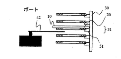
図1において、ウエハ10、およびウエハより小さな径を有するウエハ支持体20が示される。ウエハ10が、ウエハ支持体20によって完全に支持され、かつウエハボート30自体に直接接触しないように、ウエハボート30は、ウエハ支持体20およびウエハ10を収容する。
In FIG. 1, a
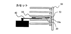
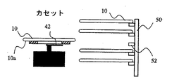
図2において、別個におよび重ね合わせたウエハ10およびウエハ支持体20の上面図が示される。ウエハ支持体20の外径は、ウエハ10の径より小さい。ウエハ支持体は、中央部分において開放領域を有する環状リングの形状を有して示されているが、ウエハ支持体がウエハの周囲に延長しないように寸法決定されている限り、ウエハ支持体は、異なる形状を有することができる。例えば、ウエハ支持体は、プレート、グリッド、またはメッシュ構造体であることができ、または外周は、円形形状から外れることができる。好ましくは、ウエハ支持体20は、360°の範囲にわたってウエハ10の周りを連続的に延びるのが好ましく、ウエハ10の外周に延びないが、ウエハ支持体20は、ウエハ10の外周に隣接しかつウエハ10の外周から挿入された連続線に実質的に沿った支持体を提供しない。さらに、ウエハ支持体20は、ウエハ10の底10a上の支持されない領域内にはまるように寸法決定され、すなわち、ウエハ支持体20は、カセット50内にウエハ10を支持するために、ウエハカセット突出部52によって妨げられない空間内にはまる。
In FIG. 2, a top view of the
図3Aから図3Fは、ウエハ支持体20上のウエハ10をウエハボート30へローディングするプロセスを概略的に示す。ウエハ支持体20は、好ましくは、ウエハ支持体20が、ウエハ10を支持するウエハカセット50の部品と接触しないように寸法決定される。好ましくは、ウエハ支持体20は、ウエハカセット50内のウエハ10の支持されていない領域の幅よりも小さい幅を有し、すなわち、ウエハ支持体20が、同平面支持体シェルフ52の内側縁部によって作られる領域の直径より小さい直径を有する。しかしながら、好ましくは、ウエハ支持体30は、ウエハ支持体30が、ウエハボート50内にローディングされた後にボートシェルフ51上に載置することができるように十分に広い。好ましくは、ウエハ支持体20は、ウエハ支持部20がウエハボート支持体シェルフ52の内側縁部を超えて延びることを可能にする直径を有する。
3A to 3F schematically show the process of loading the
図3Aにおいて、ウエハボート30は、ウエハ支持体20を収容する。ロボット40のエンドエフェクタ42は、ウエハ支持体20の下方に移動し、かつウエハ支持体20がエンドエフェクタ42上に載置されるように、ウエハ支持体20と接触するように上方向に垂直に移動する。図3Bにおいて、エンドエフェクタは、ウエハボート30の外にウエハ支持体20を取り除く。図3Cにおいて、その上にウエハ支持体20を有するエンドエフェクタ42は、ウエハカセット50内のウエハ10の下の位置に移動する。エンドエフェクタ42は、次に、ウエハ支持体20がウエハ10に接触するまで、上方向に垂直に移動する。ウエハ支持体20の小さな寸法のために、これは、ウエハ支持体20がウエハカセット50の支持体シェルフ52に接触することなく行われることができる。図3Dは、ウエハ支持体20およびウエハ10を保持するエンドエフェクタ42が、ウエハカセット50から引き出されたことを示す。図3Eにおいて、エンドエフェクタ42は、ウエハボート30に向かって移動し、かつ図3Fにおいて、エンドエフェクタは、収容器またはウエハボート30のウエハスロット31内に、ウエハ10を有するウエハ支持体20を配置する。
In FIG. 3A, the
ウエハ10をローディングした後、ウエハボート30は、好ましくはプロセッシングチャンバ(図示せず)内にローディングされ、ウエハは、半導体製造プロセスを受けることができる。有利には、半導体製造プロセスは、例えば約1000℃以上またはいくつかの実施形態において約1350℃までなどの非常に高温な熱処理でありえる。熱処理の後、アンローディングが、図3に示されるシーケンスに対して逆のシーケンスで行われることが理解される。
After loading the
好ましくは、ウエハ支持体20は、ウエハボート30内に格納され、ウエハを移送する目的で、例えばカセット50とウエハボート30との間で前後にウエハ10を移送するために、ウエハボート30から取り除かれるだけである。そのような構成は、有利には、エンドエフェクタ42が、ウエハ10を移送するために移動しなければならない移動量および距離を最小化することによって有効である。したがって、エンドエフェクタ42は、ウエハボート30とカセット50との間で移動するだけが必要である。ウエハ支持体20を収納する第3の位置に移動することは、そのような構成において必要ではない。しかしながら、代わりに、ウエハ支持体20が、使用されないときに格納されるウエハ支持体20のための1つ以上の格納カセットを提供することができる。その場合、ローディングシーケンスの開始に、ウエハ支持体20は、ウエハボート30の代わりに、ウエハ支持体格納カセットからピックアップされる。
Preferably, the
また、エンドエフェクタが、ウエハ支持体ホルダ内のスロット(例えば、ウエハボート30または別個の格納装置)と、ウエハ支持体20およびウエハ10を含むウエハカセット50との間にはまるように寸法決定されかつ形状形成される限り、従来技術で知られている様々なエンドエフェクタが、ウエハ支持体20およびウエハ10を移送するために使用されることができることが理解されよう。
Also, the end effector is dimensioned to fit between a slot in the wafer support holder (eg,
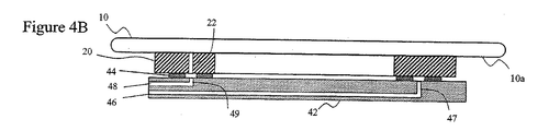
ウエハ支持体20およびウエハ10を移送する例示的なエンドエフェクタが、図4に示される。図4Aにおいて、エンドエフェクタ42が、その頂部表面に、ウエハ支持体20と接触するための接点パッド44を備える。これらのパッド44は、テフロン((商標)ポリテトラフルオロエチレン)、PEEK(商標)(ポリ・エーテル・エーテル・ケトン)、またはこの目的に適した従来技術に知られている任意の他の材料などの粒子を生成しない材料で作られることが好ましい。
An exemplary end effector for transferring
さらに、ウエハ支持体20およびウエハ10を移送するエンドエフェクタは、好ましくは、特にエンドエフェクタが移送機能の間に移動する間に、ウエハ支持体20をエンドエフェクタ上に保持する機構体が提供される。そのような機構体は、例えば、エンドエフェクタ上に載置されたウエハ支持体の移動を機械的に妨げることができる、ピン、溝、またはウエハ支持体上の突出部およびくぼみの他のマッチングパターン、およびエンドエフェクタの表面をそれぞれ含むことができる。
Furthermore, the
図示された実施形態において、ウエハ支持体の滑りを防ぐ機構体は、エンドエフェクタによって加えられる真空吸着である。例えば、図4Aに示されるように、エンドエフェクタ42は、好ましくは、1つ以上の垂直方向チャネル47と連絡する、1つ以上の水平方向チャネル46を備える。1つまたは複数の垂直方向チャネル47は、1つまたは複数のパッド44、ウエハ支持体20、およびエンドエフェクタ42の上部表面によって画定される空間に開口する。1つまたは複数のチャネル46に真空を加えることによって、真空が、支持体リング20の下側表面に加えられ、エンドエフェクタ42の水平方向の移動の間に移動することを妨げる。
In the illustrated embodiment, the mechanism that prevents slipping of the wafer support is vacuum suction applied by the end effector. For example, as shown in FIG. 4A, the
ウエハ支持体20上のウエハ10の移動を妨げるように作用する、ウエハ10とウエハ支持体20との間に摩擦力に加えて、ウエハ10は、好ましくは、エンドエフェクタ42の水平方向の移動の間に移動することをまた積極的に妨げる。これを達成する例示的な構成が、図4Bに示されている。この実施形態において、ウエハ支持体20は、垂直方向に延びる通路22を備える。水平方向チャネル48は、垂直方向チャネル49に連絡し、垂直方向チャネル49は、次に、通路22に整列されかつ通路22と連絡する。したがって、チャネル48に真空を加えることが、ウエハ10の下方表面に対する真空を結果として生じる。通路22が、気体チャネル46に接続される間に、別個の真空チャネル46および47が提供され、ウエハ支持体20およびウエハ10に加えられた真空吸着が、所望のように互いに独立して変わることができる。例えば、真空吸着が、ウエハ10がないウエハ支持体20を移送する間にウエハ支持体20だけに加えられ、またはウエハ10を保持するウエハ支持体20を移送する間にウエハ支持体20およびウエハ10に同時に加えられることができる。
In addition to the frictional force between the
さらに、通路22がウエハ支持体20を通って延びる限り、貫通通路22は、円形である必要はなく、かつ任意の断面形状であることができる。例えば、スリットの形態をとることができる。さらに、貫通通路22は、チャネル49より大きな寸法の開口を有することができ、またはチャネル49は、貫通通路22より大きな寸法の開口を有することができ、チャネル49および貫通通路22のわずかな位置ずれは、ウエハ10に加えられた真空にほとんど悪影響を与えない。さらに、チャネル49および貫通通路22を整列するために、ウエハ支持体10およびエンドエフェクタ42上、またはウエハ支持体ホルダ上、例えばウエハ30のマッチングくぼみおよび突出部、およびウエハ支持体20は、ウエハ支持体およびエンドエフェクタの位置を、他方に対する所定の固定された向きに固定するように利用されることができる。
Further, as long as the
ウエハ支持体10に対して真空吸着を提供するさらに他のエンドエフェクタの構成が、図4Cに示される。図示されるように、エンドエフェクタ42は、好ましくはウエハ10の中心に整列するように位置付けられた垂直方向に上方に延びる部分60を備える。部分60は、ウエハ10と接触するパッド45を備える。エンドエフェクタ42によってウエハ10の移送の間に、ウエハ10は、ウエハ支持体20上に支持されないが、代わりにエンドエフェクタ42の中央部分60上に支持される。この実施形態において、中央部分60は、ウエハ10の下側表面10aに真空を加えることができるように、水平方向真空チャネル48に連絡する垂直方向チャネル49が提供される。ウエハボート30内にウエハ支持体20およびウエハ10を配置するために、エンドエフェクタ42は、垂直方向下側に移動する。第1に、ウエハ支持体20は、エンドエフェクタ42が下方へ移動するにつれ、ウエハボート30に接触し、かつエンドエフェクタ42から離れるように持ち上げられる。さらにエンドエフェクタ42を下方へ移動することによって、ウエハ10は、ウエハ支持体20と接触し、かつエンドエフェクタ42から離れるように持ち上げられる。
Yet another end effector configuration that provides vacuum suction to the
図4Cに示される構成は、有利にウエハ10を確実に保持するが、いくつかの状況において、エンドエフェクタ42の垂直方向の延びる中央部分はその全体高さを追加するので、図4Bに示されるような他のエンドエフェクタ構成が好ましいことがある。これは、次に、エンドエフェクタ42とともに使用される、ウエハ10のためのスロットおよび/または任意のウエハ支持体ホルダにおけるウエハ支持体20、カセット、またはボート間に必要な最小間隔を増加する。特に、図4Cに示されるエンドエフェクタ構成を使用するとき、ウエハボートのウエハピッチは、好ましくは、図4Bに示されるエンドエフェクタを使用する構成に対して増加される。
The configuration shown in FIG. 4C advantageously holds the
上述のように、真空グリップの適用は、絶対的な要件ではないことが理解されよう。エンドエフェクタの移動の間のウエハ支持体およびウエハの移動を妨げる他の方法が可能である。そのような方法は、エンドエフェクタに限定された加速を適用すること、ハプティック材料などの滑動に対する高い抵抗を有する滑り抵抗材料を適用すること、およびウエハ支持体および/またはウエハの静電クランプを含む。さらに、例えばウエハを保持するための真空グリップと、例えばウエハ支持体の保持のためのこれらの他の方法との様々な組み合わせも可能である。 As mentioned above, it will be appreciated that the application of a vacuum grip is not an absolute requirement. Other ways of preventing wafer support and wafer movement during end effector movement are possible. Such methods include applying limited acceleration to the end effector, applying a slip resistant material having a high resistance to sliding, such as a haptic material, and electrostatic clamping of the wafer support and / or wafer. . Furthermore, various combinations of, for example, a vacuum grip for holding a wafer and these other methods for holding a wafer support, for example, are possible.
したがって、様々な他の修正、省略、および追加は、本発明の範囲を逸脱することなく、上述された方法および構造になされることができる。全てのそのような修正および変形は、添付の請求項によって規定されるように、本発明の範囲内にあることが意図される。 Accordingly, various other modifications, omissions and additions can be made to the methods and structures described above without departing from the scope of the invention. All such modifications and variations are intended to be within the scope of the invention as defined by the appended claims.
10 ウエハ
10a 底
20 ウエハ支持体
22 通路
30 ウエハ支持体、ウエハボート
31 ウエハスロット
40 ロボット
42 エンドエフェクタ
44 接点パッド
46、48 水平方向チャネル
47、49 垂直方向チャネル
50 カセット
51 ボートシェルフ
52 ウエハカセット突出部、支持体シェルフ
60 部分
DESCRIPTION OF
Claims (61)
ウエハカセット内に前記ウエハを提供することと、
ウエハ支持体ホルダ内にウエハ支持体を提供することと、
ウエハ支持体を取り除くために、前記ウエハ支持体ホルダ内にロボットエンドエフェクタを挿入することとを含み、前記ウエハ支持体は前記ロボットエンドエフェクタに載置し、方法がさらに、
前記ウエハ支持体を、前記ロボットエンドエフェクタを用いて、前記ウエハカセット内の前記ウエハの下に配置することを含み、前記ウエハ支持体が、前記ウエハと平行でありかつ前記ウエハと同軸に整列され、方法がさらに、
前記ウエハを前記ウエハ支持体上または前記エンドエフェクタ上に置くために、前記ウエハカセットに対して前記ロボットエンドエフェクタを垂直方向に移動することと、
前記ウエハ支持体および前記ウエハを保持している間、前記ロボットエンドエフェクタを前記ウエハボートに移送することと、
前記ウエハ支持体を前記ウエハボートの収容器上に配置するために、前記ウエハボートに対して前記ロボットエンドエフェクタを垂直方向に移動することとを含み、前記ウエハが、前記ウエハ支持体上に載置される方法。 A method of loading a wafer into a wafer boat,
Providing the wafer in a wafer cassette;
Providing a wafer support in a wafer support holder;
Inserting a robot end effector into the wafer support holder to remove the wafer support, the wafer support being mounted on the robot end effector, and the method further comprising:
Placing the wafer support below the wafer in the wafer cassette using the robot end effector, wherein the wafer support is parallel to the wafer and coaxially aligned with the wafer. The method is further
Moving the robot end effector vertically relative to the wafer cassette to place the wafer on the wafer support or on the end effector;
Transferring the robot end effector to the wafer boat while holding the wafer support and the wafer;
Moving the robot end effector in a vertical direction with respect to the wafer boat to place the wafer support on a container of the wafer boat, wherein the wafer is mounted on the wafer support. The way it is placed.
エンドエフェクタの上方表面に真空を発生するための開口を有するエンドエフェクタと、
前記上方表面開口と整列するように構成された通路を有するウエハ支持体と、
前記エンドエフェクタ上に前記ウエハ支持体を保持するとき、および前記ウエハ支持体上に前記ウエハを保持するときに、前記通路が、前記ウエハ支持体と前記ウエハとの境界で真空吸着を発生するように構成されるシステム。 A system for loading wafers into a wafer boat,
An end effector having an opening for generating a vacuum on an upper surface of the end effector;
A wafer support having a passage configured to align with the upper surface opening;
When the wafer support is held on the end effector, and when the wafer is held on the wafer support, the passage generates vacuum suction at the boundary between the wafer support and the wafer. System configured to.
基板縁部支持構造体上に載置する基板を提供することと、
エンドエフェクタ上に置かれた基板支持体を提供することと、
前記基板の下に前記基板支持体を配置することと、
前記基板を前記基板支持体に接触させ、かつ前記基板を前記基板支持体上に置くように、前記エンドエフェクタを上方へ移動することと、
前記基板および前記エンドエフェクタ上に置かれた前記基板支持体を、前記基板ホルダ内に配置するために、前記エンドエフェクタを移送することと、
基板支持体を前記基板ホルダ内で支持するために、前記基板支持体を支持表面上に置くように、前記エンドエフェクタを下方へ移動することとを含む方法。 A method of loading a plurality of substrates into a substrate holder for semiconductor processing,
Providing a substrate for mounting on a substrate edge support structure;
Providing a substrate support placed on an end effector;
Placing the substrate support under the substrate;
Moving the end effector upward to bring the substrate into contact with the substrate support and place the substrate on the substrate support;
Transferring the end effector to position the substrate support placed on the substrate and the end effector in the substrate holder;
Moving the end effector downward to place the substrate support on a support surface to support the substrate support in the substrate holder.
前記基板カセット内の基板の支持されていない領域の最も小さい寸法より小さい外側寸法を有する基板支持体を提供するステップと、
前記基板支持体が、前記基板に平行でありかつ前記基板の支持されていない領域と整列されるように、基板支持体を保持するロボットエンドエフェクタを、前記基板カセット内の基板の下の位置に移送するステップと、
前記基板が、前記基板支持体上または前記エンドエフェクタ上に置かれるまで、前記ロボットエンドエフェクタを上方向に垂直方向に移動するステップと、
前記基板支持体および前記基板を有する前記ロボットエンドエフェクタを、前記基板ホルダへ移送するステップと、
前記基板とともに前記基板支持体を、前記基板ホルダの収容器内へ配置するステップとを含む方法。 A method of loading a batch of substrates from one or more substrate cassettes into a substrate holder, comprising:
Providing a substrate support having an outer dimension that is less than a smallest dimension of an unsupported area of the substrate in the substrate cassette;
A robot end effector holding the substrate support is positioned below the substrate in the substrate cassette so that the substrate support is parallel to the substrate and aligned with an unsupported region of the substrate. A transporting step;
Moving the robot end effector vertically upward until the substrate is placed on the substrate support or the end effector;
Transferring the robot end effector having the substrate support and the substrate to the substrate holder;
Placing the substrate support together with the substrate into a container of the substrate holder.
実質的に平坦な底部主表面と、
前記底部主表面と平行な実質的に平坦な頂部主表面と、
前記頂部および底部主表面を接続する連続外側側壁とを備え、前記頂部および底部表面の最長寸法は、前記ウエハを格納するためのカセット内に前記ウエハを支持するために、端部支持体と同平面および端部支持体の同平面間にはまるように、ウエハ支持体が寸法決定され、前記頂部および底部表面の最長寸法は、プロセッシングの間にウエハボート内に前記ウエハ支持体を保持するために、1つ以上の水平方向延長部上に置くようにウエハ支持体が寸法決定されるウエハ支持体。 A wafer support for supporting a wafer during semiconductor processing,
A substantially flat bottom major surface;
A substantially flat top major surface parallel to the bottom major surface;
A continuous outer sidewall connecting the top and bottom major surfaces, the longest dimension of the top and bottom surfaces being the same as an end support for supporting the wafer in a cassette for storing the wafer. The wafer support is dimensioned to fit between the plane and the same plane of the end support, and the longest dimension of the top and bottom surfaces is to hold the wafer support in the wafer boat during processing. A wafer support, wherein the wafer support is dimensioned to rest on one or more horizontal extensions.
覆う対象物との境界に真空吸着を発生するように構成されたガスチャネルを有するエンドエフェクタと、
半導体プロセッシングの間に覆うウエハを、エンドエフェクタ上に置きかつ支持するように構成されるウエハ支持体とを備え、
前記ウエハ支持体が、ウエハ移送カセット内の前記ウエハを支持する縁部支持体と同平面にかつ縁部支持体間にはまるように寸法決定されるシステム。 A system for loading semiconductor wafers into a wafer boat,
An end effector having a gas channel configured to generate vacuum suction at a boundary with an object to be covered;
A wafer support configured to place and support a wafer covering during semiconductor processing on an end effector;
A system sized such that the wafer support is flush with and between the edge supports that support the wafer in a wafer transfer cassette.
Applications Claiming Priority (1)
| Application Number | Priority Date | Filing Date | Title |
|---|---|---|---|
| US49689803P | 2003-08-20 | 2003-08-20 |
Publications (2)
| Publication Number | Publication Date |
|---|---|
| JP2005123583A true JP2005123583A (en) | 2005-05-12 |
| JP2005123583A5 JP2005123583A5 (en) | 2007-09-20 |
Family
ID=34619290
Family Applications (1)
| Application Number | Title | Priority Date | Filing Date |
|---|---|---|---|
| JP2004239311A Pending JP2005123583A (en) | 2003-08-20 | 2004-08-19 | Method and system for loading substrate support into substrate holder |
Country Status (2)
| Country | Link |
|---|---|
| US (2) | US7181132B2 (en) |
| JP (1) | JP2005123583A (en) |
Cited By (2)
| Publication number | Priority date | Publication date | Assignee | Title |
|---|---|---|---|---|
| JP2007008698A (en) * | 2005-07-01 | 2007-01-18 | Ishikawajima Harima Heavy Ind Co Ltd | Substrate sucking method, substrate holder, and substrate sucking device |
| WO2016117095A1 (en) * | 2015-01-22 | 2016-07-28 | 株式会社島津製作所 | Substrate transfer system |
Families Citing this family (16)
| Publication number | Priority date | Publication date | Assignee | Title |
|---|---|---|---|---|
| US7727588B2 (en) * | 2003-09-05 | 2010-06-01 | Yield Engineering Systems, Inc. | Apparatus for the efficient coating of substrates |
| EP1790757B1 (en) * | 2004-07-22 | 2013-08-14 | Toyo Tanso Co., Ltd. | Susceptor |
| KR100946994B1 (en) | 2005-10-04 | 2010-03-10 | 가부시키가이샤 히다치 고쿠사이 덴키 | Substrate processing apparatus and manufacturing method for semiconductor devices |
| US7576653B2 (en) * | 2006-03-15 | 2009-08-18 | Angel Secure Networks, Inc. | Secure panel with remotely controlled embedded devices |
| JP4313401B2 (en) * | 2007-04-24 | 2009-08-12 | 東京エレクトロン株式会社 | Vertical heat treatment apparatus and substrate transfer method |
| US8344885B2 (en) * | 2008-01-22 | 2013-01-01 | Angel Secure Networks Inc. | Container with interior enclosure of composite material having embedded security element |
| KR20110007434A (en) * | 2009-07-16 | 2011-01-24 | 주식회사 아이피에스 | Apparatus for manufacturing semiconductor |
| EP2360720A1 (en) * | 2010-02-23 | 2011-08-24 | Saint-Gobain Glass France | Device for positioning at least two objects, assemblies in particular multi-layer body assemblies, assembly for processing, in particular selenization, of objects, method for positioning at least two objects |
| JP2012151433A (en) * | 2010-12-28 | 2012-08-09 | Tokyo Electron Ltd | Thermal treatment apparatus |
| JP5243569B2 (en) * | 2011-03-07 | 2013-07-24 | 東京エレクトロン株式会社 | Substrate transport apparatus, substrate transport method, and recording medium on which program for executing the substrate transport method is recorded |
| JP5797176B2 (en) * | 2012-09-14 | 2015-10-21 | 東京エレクトロン株式会社 | Spacer, spacer conveying method, processing method, and processing apparatus |
| DE102016113924A1 (en) | 2016-07-28 | 2018-02-01 | Infineon Technologies Ag | Wafer box, method of arranging wafers in a wafer box, wafer protection plate, and method of protecting a wafer |
| KR20200124311A (en) * | 2018-03-19 | 2020-11-02 | 도쿄엘렉트론가부시키가이샤 | Substrate holding apparatus and method for shape measurement |
| CN110673019A (en) * | 2018-12-19 | 2020-01-10 | 上海华力微电子有限公司 | Wafer-level automatic test system |
| CN112786500A (en) * | 2019-11-11 | 2021-05-11 | 夏泰鑫半导体(青岛)有限公司 | Wafer rack and vertical wafer boat with same |
| CN113707586B (en) * | 2021-08-30 | 2024-04-16 | 北京北方华创微电子装备有限公司 | Semiconductor process equipment and wafer boat storage device thereof |
Citations (4)
| Publication number | Priority date | Publication date | Assignee | Title |
|---|---|---|---|---|
| JPH10242237A (en) * | 1997-02-27 | 1998-09-11 | Nec Yamagata Ltd | Apparatus and method of transferring wafer |
| JP2003031647A (en) * | 2001-07-19 | 2003-01-31 | Hitachi Kokusai Electric Inc | Substrate processor and method for manufacturing semiconductor device |
| JP2003209153A (en) * | 2002-01-11 | 2003-07-25 | Hitachi Kokusai Electric Inc | Substrate treatment device and method for manufacturing semiconductor device |
| JP2003282388A (en) * | 2002-03-26 | 2003-10-03 | Hitachi Kokusai Electric Inc | Substrate processor, and semiconductor manufacturing method |
Family Cites Families (117)
| Publication number | Priority date | Publication date | Assignee | Title |
|---|---|---|---|---|
| AT219865B (en) | 1960-05-17 | 1962-02-26 | Plansee Metallwerk | Refractory metal susceptor for induction furnaces and process for its manufacture |
| US3466079A (en) | 1965-09-08 | 1969-09-09 | Western Electric Co | Pressurized fluid pickup device |
| US3523706A (en) | 1967-10-27 | 1970-08-11 | Ibm | Apparatus for supporting articles without structural contact and for positioning the supported articles |
| US3972704A (en) | 1971-04-19 | 1976-08-03 | Sherwood Refractories, Inc. | Apparatus for making vitreous silica receptacles |
| US3947236A (en) | 1971-11-29 | 1976-03-30 | Lasch Jr Cecil A | Fluid bearing transfer and heat treating apparatus and method |
| US4322592A (en) | 1980-08-22 | 1982-03-30 | Rca Corporation | Susceptor for heating semiconductor substrates |
| US4348044A (en) | 1980-10-10 | 1982-09-07 | Cincinnati Milacron Inc. | Article gripping apparatus |
| NL8103979A (en) | 1981-08-26 | 1983-03-16 | Bok Edward | METHOD AND APPARATUS FOR APPLYING A FILM LIQUID MEDIUM TO A SUBSTRATE |
| US4468259A (en) | 1981-12-04 | 1984-08-28 | Ushio Denki Kabushiki Kaisha | Uniform wafer heating by controlling light source and circumferential heating of wafer |
| US4407654A (en) | 1982-01-21 | 1983-10-04 | The Potters Supply Company | Handling and support system for kiln fired ware |
| NL8203318A (en) | 1982-08-24 | 1984-03-16 | Integrated Automation | DEVICE FOR PROCESSING SUBSTRATES. |
| JPS6074626A (en) | 1983-09-30 | 1985-04-26 | Fujitsu Ltd | Device for plasma treatment |
| US4563558A (en) | 1983-12-27 | 1986-01-07 | United Technologies Corporation | Directional recrystallization furnace providing convex isotherm temperature distribution |
| US4586743A (en) | 1984-09-24 | 1986-05-06 | Intelledex Incorporated | Robotic gripper for disk-shaped objects |
| FR2596070A1 (en) | 1986-03-21 | 1987-09-25 | Labo Electronique Physique | DEVICE COMPRISING A PLANAR SUSCEPTOR ROTATING PARALLEL TO A REFERENCE PLANE AROUND A PERPENDICULAR AXIS AT THIS PLAN |
| JPS62222625A (en) | 1986-03-25 | 1987-09-30 | Shimizu Constr Co Ltd | Semiconductor manufacturing equipment |
| US4770590A (en) | 1986-05-16 | 1988-09-13 | Silicon Valley Group, Inc. | Method and apparatus for transferring wafers between cassettes and a boat |
| JPS63102225A (en) | 1986-10-20 | 1988-05-07 | Deisuko Haitetsuku:Kk | Wafer boat for vertical type semiconductor thermal treatment equipment |
| JPS6387831U (en) | 1986-11-26 | 1988-06-08 | ||
| US4781411A (en) | 1987-04-23 | 1988-11-01 | Kolb James A | Portable sun shield |
| US4773687A (en) | 1987-05-22 | 1988-09-27 | American Telephone And Telegraph Company, At&T Technologies, Inc. | Wafer handler |
| GB8714175D0 (en) | 1987-06-17 | 1987-07-22 | Dynapert Precima Ltd | Suction pick-up apparatus |
| JPH0617295Y2 (en) | 1987-11-27 | 1994-05-02 | 大日本スクリーン製造株式会社 | Substrate transfer device |
| KR900006017B1 (en) | 1987-12-18 | 1990-08-20 | 한국전기통신공사 | Wafer carrier |
| US4978567A (en) | 1988-03-31 | 1990-12-18 | Materials Technology Corporation, Subsidiary Of The Carbon/Graphite Group, Inc. | Wafer holding fixture for chemical reaction processes in rapid thermal processing equipment and method for making same |
| US4900214A (en) | 1988-05-25 | 1990-02-13 | American Telephone And Telegraph Company | Method and apparatus for transporting semiconductor wafers |
| US4913481A (en) | 1988-09-13 | 1990-04-03 | Applied Power Inc. | Clean room gripper |
| JP2683675B2 (en) | 1989-01-26 | 1997-12-03 | 東京エレクトロン株式会社 | Transfer device |
| US5022695A (en) | 1989-01-30 | 1991-06-11 | Texas Instruments Incorporated | Semiconductor slice holder |
| DE3919611A1 (en) | 1989-06-15 | 1990-12-20 | Wacker Chemitronic | HOLDING DEVICE FOR RECEIVING DISC-SHAPED OBJECTS, IN PARTICULAR SEMICONDUCTOR DISC, AND METHOD FOR THEIR TREATMENT |
| ES2078269T3 (en) | 1989-06-29 | 1995-12-16 | Applied Materials Inc | APPARATUS FOR HANDLING SEMI-CONDUCTOR PLATES. |
| US5110248A (en) | 1989-07-17 | 1992-05-05 | Tokyo Electron Sagami Limited | Vertical heat-treatment apparatus having a wafer transfer mechanism |
| US5162047A (en) | 1989-08-28 | 1992-11-10 | Tokyo Electron Sagami Limited | Vertical heat treatment apparatus having wafer transfer mechanism and method for transferring wafers |
| CH680275A5 (en) | 1990-03-05 | 1992-07-31 | Tet Techno Investment Trust | |
| KR0153250B1 (en) | 1990-06-28 | 1998-12-01 | 카자마 겐쥬 | Vertical heat-treating apparatus |
| US5071485A (en) * | 1990-09-11 | 1991-12-10 | Fusion Systems Corporation | Method for photoresist stripping using reverse flow |
| US5310339A (en) | 1990-09-26 | 1994-05-10 | Tokyo Electron Limited | Heat treatment apparatus having a wafer boat |
| JPH081922B2 (en) | 1991-01-25 | 1996-01-10 | 株式会社東芝 | Wafer-holding device |
| US5192371A (en) | 1991-05-21 | 1993-03-09 | Asm Japan K.K. | Substrate supporting apparatus for a CVD apparatus |
| JPH05102056A (en) | 1991-10-11 | 1993-04-23 | Rohm Co Ltd | Wafer support jig |
| JP3234617B2 (en) | 1991-12-16 | 2001-12-04 | 東京エレクトロン株式会社 | Substrate support for heat treatment equipment |
| NL9200446A (en) | 1992-03-10 | 1993-10-01 | Tempress B V | Apparatus for handling microcircuit disks (wafers). |
| US5445486A (en) | 1992-03-29 | 1995-08-29 | Tokyo Electron Sagami Limited | Substrate transferring apparatus |
| JP3100252B2 (en) | 1992-05-26 | 2000-10-16 | 東京エレクトロン株式会社 | Object boat, method of transferring object using the same, and heat treatment apparatus |
| US5788425A (en) | 1992-07-15 | 1998-08-04 | Imation Corp. | Flexible system for handling articles |
| US5492229A (en) | 1992-11-27 | 1996-02-20 | Toshiba Ceramics Co., Ltd. | Vertical boat and a method for making the same |
| JP3348936B2 (en) | 1993-10-21 | 2002-11-20 | 東京エレクトロン株式会社 | Vertical heat treatment equipment |
| JP3125199B2 (en) | 1993-03-18 | 2001-01-15 | 東京エレクトロン株式会社 | Vertical heat treatment equipment |
| EP0634787B1 (en) | 1993-07-15 | 1997-05-02 | Applied Materials, Inc. | Subsrate tray and ceramic blade for semiconductor processing apparatus |
| US5592581A (en) | 1993-07-19 | 1997-01-07 | Tokyo Electron Kabushiki Kaisha | Heat treatment apparatus |
| US5556275A (en) | 1993-09-30 | 1996-09-17 | Tokyo Electron Limited | Heat treatment apparatus |
| AT640U1 (en) | 1993-10-22 | 1996-02-26 | Sez Semiconduct Equip Zubehoer | GRIPPERS FOR SEMICONDUCTOR WAFERS AND OTHER DISC-SHAPED ITEMS |
| US5565034A (en) | 1993-10-29 | 1996-10-15 | Tokyo Electron Limited | Apparatus for processing substrates having a film formed on a surface of the substrate |
| FI97731C (en) | 1994-11-28 | 1997-02-10 | Mikrokemia Oy | Method and apparatus for making thin films |
| DE59611078D1 (en) | 1995-03-28 | 2004-10-14 | Brooks Automation Gmbh | Loading and unloading station for semiconductor processing systems |
| US5692873A (en) | 1995-03-31 | 1997-12-02 | Motorola, Inc. | Apparatus for holding a piece of semiconductor |
| KR100278731B1 (en) | 1995-05-05 | 2001-03-02 | 보스트 스티븐 엘. | Slip resistant vertical lathe |
| JP3218164B2 (en) | 1995-05-31 | 2001-10-15 | 東京エレクトロン株式会社 | Support boat for object to be processed, heat treatment apparatus and heat treatment method |
| US5664925A (en) | 1995-07-06 | 1997-09-09 | Brooks Automation, Inc. | Batchloader for load lock |
| JPH0992625A (en) | 1995-09-20 | 1997-04-04 | Tokyo Electron Ltd | Boat for heat treatment |
| SE9503426D0 (en) | 1995-10-04 | 1995-10-04 | Abb Research Ltd | A device for heat treatment of objects and a method for producing a susceptor |
| US5984607A (en) | 1995-11-06 | 1999-11-16 | Tokyo Electron Limited | Transfer apparatus, transfer method, treatment apparatus and treatment method |
| US5746460A (en) | 1995-12-08 | 1998-05-05 | Applied Materials, Inc. | End effector for semiconductor wafer transfer device and method of moving a wafer with an end effector |
| KR0165350B1 (en) | 1995-12-13 | 1999-02-18 | 김광호 | Semiconductor wafer supply system |
| TW321192U (en) | 1995-12-23 | 1997-11-21 | Samsung Electronics Co Ltd | A arm of robot for transporting semiconductor wafer |
| KR100443415B1 (en) | 1996-02-23 | 2004-11-03 | 동경 엘렉트론 주식회사 | Heat treatment device |
| SE9600705D0 (en) | 1996-02-26 | 1996-02-26 | Abb Research Ltd | A susceptor for a device for epitaxially growing objects and such a device |
| KR19990077350A (en) | 1996-02-29 | 1999-10-25 | 히가시 데쓰로 | Heat treatment boat of semiconductor wafer |
| JPH09306980A (en) | 1996-05-17 | 1997-11-28 | Asahi Glass Co Ltd | Vertical wafer boat |
| US5788453A (en) | 1996-05-30 | 1998-08-04 | Applied Materials, Inc. | Piezoelectric wafer gripping system for robot blades |
| US5851041A (en) | 1996-06-26 | 1998-12-22 | Ontrak Systems, Inc. | Wafer holder with spindle assembly and wafer holder actuator |
| JP2772283B2 (en) | 1996-07-16 | 1998-07-02 | 山形日本電気株式会社 | Vacuum suction tweezers and suction method |
| US5848889A (en) | 1996-07-24 | 1998-12-15 | Applied Materials Inc. | Semiconductor wafer support with graded thermal mass |
| JPH1074818A (en) | 1996-09-02 | 1998-03-17 | Tokyo Electron Ltd | Treating device |
| US6183183B1 (en) | 1997-01-16 | 2001-02-06 | Asm America, Inc. | Dual arm linear hand-off wafer transfer assembly |
| US5983906A (en) | 1997-01-24 | 1999-11-16 | Applied Materials, Inc. | Methods and apparatus for a cleaning process in a high temperature, corrosive, plasma environment |
| JPH10233426A (en) | 1997-02-20 | 1998-09-02 | Tokyo Electron Ltd | Automatic teaching method |
| NL1005410C2 (en) | 1997-02-28 | 1998-08-31 | Advanced Semiconductor Mat | System for loading, handling and unloading substrates mounted on a support. |
| US5879459A (en) | 1997-08-29 | 1999-03-09 | Genus, Inc. | Vertically-stacked process reactor and cluster tool system for atomic layer deposition |
| TW401582B (en) | 1997-05-15 | 2000-08-11 | Tokyo Electorn Limtied | Apparatus for and method of transferring substrates |
| AT405701B (en) | 1997-06-18 | 1999-11-25 | Sez Semiconduct Equip Zubehoer | GRIPPERS FOR SEMICONDUCTOR WAFERS AND OTHER DISC-SHAPED ITEMS |
| US5839770A (en) | 1997-06-26 | 1998-11-24 | Zaytran, Inc. | Robotic gripper |
| US6034000A (en) | 1997-07-28 | 2000-03-07 | Applied Materials, Inc. | Multiple loadlock system |
| US6321680B2 (en) | 1997-08-11 | 2001-11-27 | Torrex Equipment Corporation | Vertical plasma enhanced process apparatus and method |
| US6068441A (en) | 1997-11-21 | 2000-05-30 | Asm America, Inc. | Substrate transfer system for semiconductor processing equipment |
| JPH11176822A (en) | 1997-12-05 | 1999-07-02 | Hitachi Ltd | Semiconductor treating equipment |
| US6204194B1 (en) | 1998-01-16 | 2001-03-20 | F.T.L. Co., Ltd. | Method and apparatus for producing a semiconductor device |
| US5931666A (en) | 1998-02-27 | 1999-08-03 | Saint-Gobain Industrial Ceramics, Inc. | Slip free vertical rack design having rounded horizontal arms |
| US6203617B1 (en) | 1998-03-26 | 2001-03-20 | Tokyo Electron Limited | Conveying unit and substrate processing unit |
| US6280183B1 (en) | 1998-04-01 | 2001-08-28 | Applied Materials, Inc. | Substrate support for a thermal processing chamber |
| US6109677A (en) | 1998-05-28 | 2000-08-29 | Sez North America, Inc. | Apparatus for handling and transporting plate like substrates |
| KR20000002833A (en) | 1998-06-23 | 2000-01-15 | 윤종용 | Semiconductor wafer boat |
| US6158951A (en) | 1998-07-10 | 2000-12-12 | Asm America, Inc. | Wafer carrier and method for handling of wafers with minimal contact |
| US6167322A (en) | 1998-07-10 | 2000-12-26 | Holbrooks; Orville Ray | Intelligent wafer handling system and method |
| KR100331157B1 (en) | 1998-07-24 | 2002-04-03 | 다니구찌 이찌로오, 기타오카 다카시 | Wafer holding hand |
| US6228173B1 (en) | 1998-10-12 | 2001-05-08 | Tokyo Electron Limited | Single-substrate-heat-treating apparatus for semiconductor process system |
| US5990650A (en) | 1998-11-25 | 1999-11-23 | Lumonics Corporation | Method and apparatus for orienting a disk via edge contact |
| US6168668B1 (en) | 1998-11-25 | 2001-01-02 | Applied Materials, Inc. | Shadow ring and guide for supporting the shadow ring in a chamber |
| JP2000183133A (en) | 1998-12-15 | 2000-06-30 | Tokyo Seimitsu Co Ltd | Robot hand |
| NL1012004C2 (en) | 1999-05-07 | 2000-11-13 | Asm Int | Method for moving wafers as well as ring. |
| US6279976B1 (en) | 1999-05-13 | 2001-08-28 | Micron Technology, Inc. | Wafer handling device having conforming perimeter seal |
| US6322116B1 (en) | 1999-07-23 | 2001-11-27 | Asm America, Inc. | Non-contact end effector |
| TWI250604B (en) | 1999-07-29 | 2006-03-01 | Ibm | Improved ladder boat for supporting wafers |
| US6244641B1 (en) | 1999-12-02 | 2001-06-12 | M.E.C. Technology, Inc. | Wafer transfer arm |
| US6347919B1 (en) | 1999-12-17 | 2002-02-19 | Eaton Corporation | Wafer processing chamber having separable upper and lower halves |
| JP2001176808A (en) | 1999-12-21 | 2001-06-29 | Toshiba Ceramics Co Ltd | Method for wafer conveyance of vapor-phase thin-film growth device and wafer support member used therefor |
| US6331023B1 (en) | 2000-01-14 | 2001-12-18 | Asm America, Inc. | Gridded substrate transport spatula |
| US7125477B2 (en) * | 2000-02-17 | 2006-10-24 | Applied Materials, Inc. | Contacts for electrochemical processing |
| US6287112B1 (en) | 2000-03-30 | 2001-09-11 | Asm International, N.V. | Wafer boat |
| US6341935B1 (en) | 2000-06-14 | 2002-01-29 | Taiwan Semiconductor Manufacturing Company, Ltd. | Wafer boat having improved wafer holding capability |
| JP2002033284A (en) | 2000-07-14 | 2002-01-31 | Mitsui Eng & Shipbuild Co Ltd | Wafer holder for vertical cvd |
| US6464445B2 (en) | 2000-12-19 | 2002-10-15 | Infineon Technologies Richmond, Lp | System and method for improved throughput of semiconductor wafer processing |
| US6559039B2 (en) | 2001-05-15 | 2003-05-06 | Applied Materials, Inc. | Doped silicon deposition process in resistively heated single wafer chamber |
| US6753506B2 (en) * | 2001-08-23 | 2004-06-22 | Axcelis Technologies | System and method of fast ambient switching for rapid thermal processing |
| US6835039B2 (en) | 2002-03-15 | 2004-12-28 | Asm International N.V. | Method and apparatus for batch processing of wafers in a furnace |
| US7256375B2 (en) | 2002-08-30 | 2007-08-14 | Asm International N.V. | Susceptor plate for high temperature heat treatment |
| KR100491161B1 (en) * | 2002-11-26 | 2005-05-24 | 주식회사 테라세미콘 | Semiconductor manufacturing system for thermal process |
-
2004
- 2004-08-05 US US10/913,945 patent/US7181132B2/en active Active
- 2004-08-19 JP JP2004239311A patent/JP2005123583A/en active Pending
-
2007
- 2007-01-31 US US11/669,842 patent/US7570876B2/en active Active
Patent Citations (4)
| Publication number | Priority date | Publication date | Assignee | Title |
|---|---|---|---|---|
| JPH10242237A (en) * | 1997-02-27 | 1998-09-11 | Nec Yamagata Ltd | Apparatus and method of transferring wafer |
| JP2003031647A (en) * | 2001-07-19 | 2003-01-31 | Hitachi Kokusai Electric Inc | Substrate processor and method for manufacturing semiconductor device |
| JP2003209153A (en) * | 2002-01-11 | 2003-07-25 | Hitachi Kokusai Electric Inc | Substrate treatment device and method for manufacturing semiconductor device |
| JP2003282388A (en) * | 2002-03-26 | 2003-10-03 | Hitachi Kokusai Electric Inc | Substrate processor, and semiconductor manufacturing method |
Cited By (3)
| Publication number | Priority date | Publication date | Assignee | Title |
|---|---|---|---|---|
| JP2007008698A (en) * | 2005-07-01 | 2007-01-18 | Ishikawajima Harima Heavy Ind Co Ltd | Substrate sucking method, substrate holder, and substrate sucking device |
| WO2016117095A1 (en) * | 2015-01-22 | 2016-07-28 | 株式会社島津製作所 | Substrate transfer system |
| JPWO2016117095A1 (en) * | 2015-01-22 | 2017-06-15 | 株式会社島津製作所 | Substrate transfer system |
Also Published As
| Publication number | Publication date |
|---|---|
| US20050062465A1 (en) | 2005-03-24 |
| US7181132B2 (en) | 2007-02-20 |
| US7570876B2 (en) | 2009-08-04 |
| US20070122128A1 (en) | 2007-05-31 |
Similar Documents
| Publication | Publication Date | Title |
|---|---|---|
| US7570876B2 (en) | Method and system for loading substrate supports into a substrate holder | |
| JP4575647B2 (en) | Method and apparatus for batch processing wafers in a furnace | |
| JP4632551B2 (en) | Wafer and ring transfer method, heat treatment equipment ring combination, and wafer and ring set | |
| TWI462145B (en) | Vertical type heat processing apparatus and vertical type heat processing method | |
| KR101736854B1 (en) | Substrate treating apparatus | |
| KR102120521B1 (en) | Wafer boat support table and heat treatment apparatus using the same | |
| US20080025835A1 (en) | Bernoulli wand | |
| JP2002536201A (en) | Apparatus and method for handling substrates by a self-leveling vacuum system in an epitaxial induction reactor with a flat disk-shaped susceptor | |
| JP2008187017A (en) | Vertical heat treatment apparatus and vertical heat treatment method | |
| CN108666232B (en) | Substrate processing system, substrate turnover device and method | |
| US6158951A (en) | Wafer carrier and method for handling of wafers with minimal contact | |
| JP2009099996A (en) | Vertical heat treatment system and method of transferring workpieces | |
| US7104578B2 (en) | Two level end effector | |
| KR102514452B1 (en) | Cooling unit, substrate treating apparatus including the same, and substrate treating method using the same | |
| JPH0661331A (en) | Substrate transfer system | |
| JP3157738B2 (en) | Wafer transfer device and transfer method | |
| JP3373394B2 (en) | Substrate processing apparatus and substrate processing method | |
| JP4358690B2 (en) | Vertical heat treatment apparatus and operation method thereof | |
| JP2630366B2 (en) | Loading / unloading method and loading / unloading device for plate-like body | |
| JP2639424B2 (en) | Transport method | |
| JP2008235810A (en) | Heat treatment method, heat treatment device, and method for transferring substrate to be treated | |
| WO2020137170A1 (en) | Vapor phase growth device | |
| KR101578081B1 (en) | Wafer processing system | |
| JP5031960B2 (en) | Substrate processing apparatus and semiconductor device manufacturing method | |
| JP2004071618A (en) | Substrate treating device |
Legal Events
| Date | Code | Title | Description |
|---|---|---|---|
| A521 | Written amendment |
Free format text: JAPANESE INTERMEDIATE CODE: A523 Effective date: 20070801 |
|
| A621 | Written request for application examination |
Free format text: JAPANESE INTERMEDIATE CODE: A621 Effective date: 20070801 |
|
| RD02 | Notification of acceptance of power of attorney |
Free format text: JAPANESE INTERMEDIATE CODE: A7422 Effective date: 20090807 |
|
| RD03 | Notification of appointment of power of attorney |
Free format text: JAPANESE INTERMEDIATE CODE: A7423 Effective date: 20090807 |
|
| RD04 | Notification of resignation of power of attorney |
Free format text: JAPANESE INTERMEDIATE CODE: A7424 Effective date: 20091225 |
|
| A131 | Notification of reasons for refusal |
Free format text: JAPANESE INTERMEDIATE CODE: A131 Effective date: 20100309 |
|
| A02 | Decision of refusal |
Free format text: JAPANESE INTERMEDIATE CODE: A02 Effective date: 20100803 |