JP2005116363A - Plasma display panel - Google Patents
Plasma display panel Download PDFInfo
- Publication number
- JP2005116363A JP2005116363A JP2003349749A JP2003349749A JP2005116363A JP 2005116363 A JP2005116363 A JP 2005116363A JP 2003349749 A JP2003349749 A JP 2003349749A JP 2003349749 A JP2003349749 A JP 2003349749A JP 2005116363 A JP2005116363 A JP 2005116363A
- Authority
- JP
- Japan
- Prior art keywords
- blue
- plasma display
- emitting phosphor
- blue light
- display panel
- Prior art date
- Legal status (The legal status is an assumption and is not a legal conclusion. Google has not performed a legal analysis and makes no representation as to the accuracy of the status listed.)
- Pending
Links
Images


Classifications
-
- C—CHEMISTRY; METALLURGY
- C09—DYES; PAINTS; POLISHES; NATURAL RESINS; ADHESIVES; COMPOSITIONS NOT OTHERWISE PROVIDED FOR; APPLICATIONS OF MATERIALS NOT OTHERWISE PROVIDED FOR
- C09K—MATERIALS FOR MISCELLANEOUS APPLICATIONS, NOT PROVIDED FOR ELSEWHERE
- C09K11/00—Luminescent, e.g. electroluminescent, chemiluminescent materials
- C09K11/08—Luminescent, e.g. electroluminescent, chemiluminescent materials containing inorganic luminescent materials
- C09K11/77—Luminescent, e.g. electroluminescent, chemiluminescent materials containing inorganic luminescent materials containing rare earth metals
- C09K11/7728—Luminescent, e.g. electroluminescent, chemiluminescent materials containing inorganic luminescent materials containing rare earth metals containing europium
- C09K11/7734—Aluminates
-
- C—CHEMISTRY; METALLURGY
- C09—DYES; PAINTS; POLISHES; NATURAL RESINS; ADHESIVES; COMPOSITIONS NOT OTHERWISE PROVIDED FOR; APPLICATIONS OF MATERIALS NOT OTHERWISE PROVIDED FOR
- C09K—MATERIALS FOR MISCELLANEOUS APPLICATIONS, NOT PROVIDED FOR ELSEWHERE
- C09K11/00—Luminescent, e.g. electroluminescent, chemiluminescent materials
- C09K11/08—Luminescent, e.g. electroluminescent, chemiluminescent materials containing inorganic luminescent materials
- C09K11/77—Luminescent, e.g. electroluminescent, chemiluminescent materials containing inorganic luminescent materials containing rare earth metals
- C09K11/7728—Luminescent, e.g. electroluminescent, chemiluminescent materials containing inorganic luminescent materials containing rare earth metals containing europium
- C09K11/77342—Silicates
-
- H—ELECTRICITY
- H01—ELECTRIC ELEMENTS
- H01J—ELECTRIC DISCHARGE TUBES OR DISCHARGE LAMPS
- H01J11/00—Gas-filled discharge tubes with alternating current induction of the discharge, e.g. alternating current plasma display panels [AC-PDP]; Gas-filled discharge tubes without any main electrode inside the vessel; Gas-filled discharge tubes with at least one main electrode outside the vessel
- H01J11/10—AC-PDPs with at least one main electrode being out of contact with the plasma
- H01J11/12—AC-PDPs with at least one main electrode being out of contact with the plasma with main electrodes provided on both sides of the discharge space
-
- H—ELECTRICITY
- H01—ELECTRIC ELEMENTS
- H01J—ELECTRIC DISCHARGE TUBES OR DISCHARGE LAMPS
- H01J11/00—Gas-filled discharge tubes with alternating current induction of the discharge, e.g. alternating current plasma display panels [AC-PDP]; Gas-filled discharge tubes without any main electrode inside the vessel; Gas-filled discharge tubes with at least one main electrode outside the vessel
- H01J11/20—Constructional details
- H01J11/34—Vessels, containers or parts thereof, e.g. substrates
- H01J11/42—Fluorescent layers
Landscapes
- Chemical & Material Sciences (AREA)
- Engineering & Computer Science (AREA)
- Inorganic Chemistry (AREA)
- Materials Engineering (AREA)
- Organic Chemistry (AREA)
- Physics & Mathematics (AREA)
- Plasma & Fusion (AREA)
- Gas-Filled Discharge Tubes (AREA)
- Luminescent Compositions (AREA)
- Control Of Indicators Other Than Cathode Ray Tubes (AREA)
- Control Of Gas Discharge Display Tubes (AREA)
Abstract
Description
本発明はプラズマディスプレイパネルに関し、特に、プラズマディスプレイパネルの一構成要素である蛍光体層のうちの青色蛍光体層の物理的組成に関する。 The present invention relates to a plasma display panel, and more particularly, to a physical composition of a blue phosphor layer among phosphor layers that are components of a plasma display panel.
プラズマディスプレイパネル(以下、「PDP」ともいう)は、薄型で大画面表示を比較的容易に行うことできること、視野角が広いこと、応答速度が速いことその他の特徴を有しているため、近時、フラットディスプレイとしての用途が広がっている。 A plasma display panel (hereinafter also referred to as “PDP”) has other features such as being thin and capable of displaying a large screen relatively easily, having a wide viewing angle, and having a high response speed. At times, its use as a flat display is expanding.
図4は、一般的な3電極面放電交流型プラズマディスプレイパネル300における1つの表示セルの構成を示す斜視図である。
FIG. 4 is a perspective view showing a configuration of one display cell in a general three-electrode surface discharge AC type
図4に示すように、この表示セルにおいては、前面基板351と背面基板352とが相互に平行に設けられている。プラズマディスプレイパネル300が用いられるときには、前面基板351が看者の方を向くように配置される。
As shown in FIG. 4, in this display cell, a
前面基板351は、ガラスその他の透明材料により形成された絶縁基板302と、絶縁基板302における背面基板352に対向する表面上に形成された複数個の走査電極303及び共通電極304(図4においては、走査電極303及び共通電極304はそれぞれ1つのみ図示)と、走査電極303上に形成されたトレース電極305と、共通電極304上に形成されたトレース電極306と、走査電極303、共通電極304、トレース電極305及び306を覆って絶縁基板302上に形成された誘電体層312と、誘電体層312上に形成された保護層313と、を備えている。
The
走査電極303及び共通電極304は所定の間隔を隔てて、相互に平行に、かつ、交互に配置されている。
The
トレース電極305及び306は走査電極303上及び共通電極304の電極抵抗値を小さくするために形成された電極である。
保護層313は、誘電体層312を放電から保護するために形成されており、例えば、酸化マグネシウム(MgO)からなる。
The
背面基板352は、ガラスその他の透明材料からなる絶縁基板301と、絶縁基板301の前面基板351に対向する表面において、走査電極303及び共通電極304に直交する方向に延びるように形成された複数個のデータ電極307(図4においては、データ電極307は1つのみ図示)と、データ電極307を覆って絶縁基板301上に形成された誘電体層314と、誘電体層314上に形成された隔壁315と、誘電体層314の表面及び隔壁315の側面に形成された蛍光体層311と、から構成されている。
The
図4に示した表示セルにおいては、背面基板352は透明の絶縁基板301を備えるものとして形成されているが、必ずしも透明基板を用いる必要はない。
In the display cell shown in FIG. 4, the
隔壁315は、放電ガス空間を確保するとともに、表示セル(画素)308を区画している。
The
絶縁基板301の表面に垂直な方向から見て、隔壁315は井桁状(格子状)に形成されている。隔壁315は、データ電極317が延びる方向と同一の方向に延びる縦隔壁315aと、縦隔壁315aが延びる方向に直交する方向に延びる横隔壁315bとからなっている。
When viewed from a direction perpendicular to the surface of the
縦隔壁315aの高さと横隔壁315bの高さは相互にほぼ等しく、絶縁基板301の表面からの高さ、すなわち、誘電体層314及び隔壁315の合計膜厚は、例えば、120μmである。
The height of the
表示セル308にはヘリウム、ネオンもしくはキセノンその他の希ガス又はこれらの希ガスの混合ガスからなる放電ガスが充填されている。蛍光体層311は、この放電ガスの放電によって発生する紫外線を受けて、看者に向けて可視光310を発光する。
The
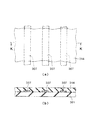
図5、図6及び図7は図4に示したプラズマディスプレイパネル300の製造方法を示す図であり、各図の(a)は背面基板352を示す平面図であり、(b)はそれぞれJ−J線、K−K線、L−L線の断面図である。以下、図5、図6及び図7を参照して、プラズマディスプレイパネル300の製造方法を説明する。
5, FIG. 6 and FIG. 7 are diagrams showing a method of manufacturing the
図4に示すように、先ず、絶縁基板302上に走査電極303及び共通電極304を相互に平行な方向に延び、かつ、交互に配置されるよう形成する。
As shown in FIG. 4, first,
次いで、走査電極303及び共通電極304上にそれぞれトレース電極305及び306を形成する。
Next,
次いで、走査電極303、共通電極304及びトレース電極305及び306を覆うように、絶縁基板302上に誘電体層312を形成する。
Next, a
次いで、誘電体層312上にMgOからなる保護層313を形成する。
Next, a
これにより、前面基板351が作製される。
Thereby, the
一方、背面基板352に関しては、図5(a)及び(b)に示すように、絶縁基板301上に一方向に延びる複数個のデータ電極307を形成する。
On the other hand, for the
次に、図6(a)及び(b)に示すように、このデータ電極307を覆うように絶縁基板301上に誘電体層314を形成する。
Next, as shown in FIGS. 6A and 6B, a
次に、図7(a)及び(b)に示すように、誘電体層314上に隔壁315を形成する。
Next, as shown in FIGS. 7A and 7B, a
隔壁315の形成方法としては、サンドブラスト法及び印刷法があるが、例えば、サンドブラスト法を用いる場合には、隔壁315は以下のようにして形成される。
As a method of forming the
先ず、フィラー、ガラス粉末、バインダー及び溶剤が混合されてなる隔壁ペーストを作製する。 First, a barrier rib paste in which a filler, glass powder, a binder and a solvent are mixed is prepared.
次に、この隔壁ペーストを誘電体層314上に塗布し、隔壁ペースト中の溶剤を揮発させ、隔壁ペースト層(図示せず)を形成する。
Next, this barrier rib paste is applied onto the
次に、この隔壁ペースト層上にドライフィルム(図示せず)を貼付し、このドライフィルムをパターニングする。 Next, a dry film (not shown) is stuck on the partition wall paste layer, and the dry film is patterned.
次に、このパターニングされたドライフィルムをマスクとしてサンドブラストを行い、隔壁ペースト層を選択的に除去してパターニングを行う。 Next, sand blasting is performed using the patterned dry film as a mask, and the partition paste layer is selectively removed to perform patterning.
その後、ドライフィルムを除去し、隔壁ペースト層を焼成する。 Thereafter, the dry film is removed and the partition paste layer is fired.
これにより、隔壁ペースト層中のバインダーが蒸発するとともに、ガラス粉末が溶解・再凝固し、フィラー及びガラスからなる隔壁315を形成することができる。
As a result, the binder in the partition paste layer evaporates, and the glass powder is melted and re-solidified to form the
隔壁315は、縦隔壁315aの高さと横隔壁315bの高さとが相互にほぼ等しくなるように、井桁状に形成される。
The
次に、図4に示すように、誘電体層314の表面及び隔壁315の側面に蛍光体層311を形成する。
Next, as shown in FIG. 4, a
その後、絶縁基板301を絶縁基板302に重ね合わせ、絶縁基板302上に形成された保護層313に、絶縁基板301上に形成された隔壁315を当接させる。このとき、データ電極307が延びる方向が走査電極303及び共通電極304が延びる方向に対して直交するようにする。
After that, the
次に、絶縁基板301と絶縁基板302とを重ね合わせた状態で熱処理を施し、絶縁基板301及び302の端部同士をフリットにより融着する。これにより、絶縁基板301、絶縁基板302及びフリットからなる封止層(図示せず)に囲まれた空間を気密的に封止する。
Next, heat treatment is performed in a state where the
この後、この空間内を排気し、この空間内に放電ガスを充填する。 Thereafter, the space is evacuated and the space is filled with a discharge gas.
これにより、図4に示したプラズマディスプレイパネル300が作製される。
Thereby, the
カラープラズマディスプレイパネルを作成する場合には、蛍光体層311は各表示セル毎にRGBに配色される。すなわち、赤色発光蛍光体からなる蛍光体層と、緑色発光蛍光体からなる蛍光体層と、青色発光蛍光体からなる蛍光体層とがこの順番に縦及び横方向に配列される。
When creating a color plasma display panel, the
これら3色の蛍光体層のうち、青色蛍光体層については、初期輝度と寿命とが相反する課題として未解決のまま残されている。すなわち、これまでは、青色蛍光体層の初期輝度を重視して、青色蛍光体層の構成材料を選択すると、青色蛍光体層の長寿命は得られず、寿命が短くなることが避けられず、逆に、青色蛍光体層の寿命を重視して、青色蛍光体層の構成材料を選択すると、青色蛍光体層の初期輝度は低くならざるを得なかった。 Of these three color phosphor layers, the blue phosphor layer is left unresolved as a problem in which the initial luminance and the lifetime conflict. In other words, until now, if the material for the blue phosphor layer is selected with emphasis on the initial luminance of the blue phosphor layer, the long life of the blue phosphor layer cannot be obtained, and it is inevitable that the lifetime will be shortened. On the contrary, when the constituent material of the blue phosphor layer is selected with emphasis on the lifetime of the blue phosphor layer, the initial luminance of the blue phosphor layer has to be lowered.
このため、青色蛍光体層に関するこのような問題を解決するためにこれまでに種々の提案がなされている。 For this reason, various proposals have been made so far in order to solve such problems related to the blue phosphor layer.
例えば、特開2002−332481号公報(特許文献1)は、青色蛍光体層の構成材料として、珪酸塩系の真空紫外線励起蛍光体を提案している。 For example, JP-A-2002-332481 (Patent Document 1) proposes a silicate-based vacuum ultraviolet-excited phosphor as a constituent material of a blue phosphor layer.
また、特開2001−84911号公報(特許文献2)は、発光色の異なる蛍光体を混合して蛍光体層を形成したプラズマディスプレイパネルを提案している。
具体的には、特許文献1は、一般式mM1O・nM2O・2M3O2(式中のM1はCa、Sr及びBaからなる群より選ばれる1種以上、M2はMg及びZnからなる群より選ばれる1種以上、M3はSi及びGeからなる群より選ばれる1種以上、0.5≦m≦3.5、0.5≦n≦2.5、ただし、m=n=1のときはM1はCa、Sr及びBaからなる群より選ばれる2種以上またはSrまたはBaである)で表される化合物に付活剤としてEu、Mnからなる群より選ばれる1種以上が含有されてなることを特徴とする真空紫外線励起発光素子用の蛍光体を提案している。
Specifically,
また、特許文献2は、赤色蛍光体層、緑色蛍光体層及び青色蛍光体層の少なくとも一つが、当該発光色の蛍光体と、当該発光色以外の発光色の蛍光体を混合した混合蛍光体層で構成されているプラズマディスプレイパネルを提案している。
特許文献1に記載されている珪酸塩系の真空紫外線励起蛍光体は輝度の経時変化は小さいという利点を有する代わりに、初期輝度が低いという欠点を有している。
The silicate-based vacuum ultraviolet-excited phosphor described in
特許文献1は、熱処理やプラズマ暴露に起因する輝度の経時変化を抑制することを目的としているため、珪酸塩系の真空紫外線励起蛍光体を用いることにより、この目的を達成することが可能ではある。しかしながら、輝度の経時変化の抑制を達成することに伴って、初期輝度の犠牲を必然的に伴う結果となっている。
Since
また、特許文献2は、白色発光時、すなわち、赤色、緑色及び青色の3色の発光時における色座標(色温度)を制御することを目的としている。蛍光体層を、一つの発光色の蛍光体と、他の発光色の蛍光体との混合物から構成することにより、この目的を達成することは可能ではあるが、それと引き換えに、青色を単色で発光させたときの色味(色度)が低下する結果となっている。
本発明は、以上のような従来のプラズマディスプレイパネルにおける問題点に鑑みてなされたものであって、初期輝度を大きく低下させることなく、輝度の経時変化を抑制することが可能なプラズマディスプレイパネル及びそのプラズマディスプレイパネルを備えるプラズマ表示装置を提供することを目的とする。 The present invention has been made in view of the problems in the conventional plasma display panel as described above, and a plasma display panel capable of suppressing a change in luminance with time without greatly reducing the initial luminance. An object of the present invention is to provide a plasma display device including the plasma display panel.
この目的を達成するため、本発明は、表示側の第一基板と、この第一基板と対向して配置された第二基板とからなるプラズマディスプレイパネルであって、前記第一基板は、透明基板と、前記透明基板上において前記第二基板に対向して形成された走査電極及び共通電極と、前記透明基板、前記走査電極及び前記共通電極を覆って形成された誘電体層と、からなり、前記第二基板は、絶縁性基板と、前記絶縁性基板上に形成された複数のデータ電極と、前記絶縁性基板上に形成された複数の隔壁と、相互に隣接する前記隔壁の間において前記絶縁性基板及び前記データ電極を覆って形成された蛍光体層と、からなり、前記蛍光体層は少なくとも青色発光蛍光体からなる青色蛍光体層を含み、前記青色蛍光体層は、初期輝度及び輝度の経時変化の双方が相互に異なる2種類以上の青色発光蛍光体の混合物からなるものであるプラズマディスプレイパネルを提供する。 In order to achieve this object, the present invention provides a plasma display panel comprising a display-side first substrate and a second substrate disposed opposite to the first substrate, wherein the first substrate is transparent. A substrate, a scan electrode and a common electrode formed on the transparent substrate so as to face the second substrate, and a dielectric layer formed to cover the transparent substrate, the scan electrode, and the common electrode. The second substrate includes an insulating substrate, a plurality of data electrodes formed on the insulating substrate, a plurality of barrier ribs formed on the insulating substrate, and the barrier ribs adjacent to each other. A phosphor layer formed to cover the insulating substrate and the data electrode, and the phosphor layer includes a blue phosphor layer made of at least a blue light-emitting phosphor, and the blue phosphor layer has an initial luminance. And luminance change over time Both to provide a plasma display panel is made of a mixture of two or more kinds of the blue emitting phosphor with each other.
本発明に係るプラズマディスプレイパネルにおいては、蛍光体層を構成する青色蛍光体層は初期輝度及び輝度の経時変化の双方が相互に異なる2種類以上の青色発光蛍光体の混合物からなる。 In the plasma display panel according to the present invention, the blue phosphor layer constituting the phosphor layer is composed of a mixture of two or more types of blue light emitting phosphors that are different from each other in both initial luminance and luminance with time.
なお、輝度の経時変化は青色蛍光体層の寿命と同義である。すなわち、輝度の経時変化が大きくなるほど、寿命は短くなり、逆に、輝度の経時変化が小さくなるほど、寿命は長くなる。 The change in luminance with time is synonymous with the lifetime of the blue phosphor layer. That is, the longer the luminance changes with time, the shorter the lifetime, and conversely, the smaller the luminance changes with time, the longer the lifetime.
一般に、青色発光蛍光体においては、初期輝度特性と輝度の経時変化特性とは両立しない。すなわち、初期輝度が高ければ、輝度の経時変化は大きい(すなわち、寿命は短い)ことが多く、逆に、初期輝度が低ければ、輝度の経時変化は小さい(すなわち、寿命は長い)ことが多い。このため、初期輝度が高く、従って、輝度の経時変化も大きい第一の青色発光蛍光体と、初期輝度が低く、従って、輝度の経時変化も小さい第二の青色発光蛍光体とを適当な比率で混合させることにより、初期輝度及び輝度の経時変化を所望の通りに制御することができる。 In general, in the blue light emitting phosphor, the initial luminance characteristic and the luminance change characteristic with time are not compatible. That is, if the initial luminance is high, the luminance change with time is often large (that is, the lifetime is short). Conversely, if the initial luminance is low, the luminance change with time is often small (that is, the lifetime is long). . Therefore, an appropriate ratio of the first blue light-emitting phosphor having a high initial luminance and therefore a large change in luminance with time and the second blue light-emitting phosphor having a low initial luminance and therefore a small change in luminance with time. By mixing with, the initial luminance and changes with time in luminance can be controlled as desired.
なお、混合する青色発光蛍光体の種類の数は2でもよく、あるいは、3以上とすることもできる。 Note that the number of types of blue-emitting phosphors to be mixed may be two, or three or more.
例えば、前記青色蛍光体層は、第一の青色発光蛍光体と、前記第一の青色発光蛍光体の初期輝度よりも初期輝度が低く、かつ、前記第一の青色発光蛍光体の輝度の経時変化よりも経時変化が小さい第二の青色発光蛍光体との混合物からなるものとすることができる。 For example, the blue phosphor layer has an initial luminance lower than an initial luminance of the first blue light-emitting phosphor and the first blue light-emitting phosphor, and the luminance of the first blue light-emitting phosphor is changed over time. It can consist of a mixture with the 2nd blue light emission fluorescent substance whose change with time is smaller than change.
このように、初期輝度と輝度の経時変化とが相互に異なる二種類の青色発光蛍光体を混合することにより、所望の初期輝度及び輝度の経時変化を有する青色蛍光体層を得ることができる。この場合、混合比率は用途に応じて決めることができる。例えば、初期輝度を重視する場合には、第一の青色発光蛍光体の混合比率を大きくすればよく、逆に、輝度の経時変化を重視する場合には、第二の青色発光蛍光体の混合比率を大きくすればよい。 Thus, by mixing two kinds of blue light emitting phosphors having different initial luminance and luminance change with time, a blue phosphor layer having desired initial luminance and luminance change with time can be obtained. In this case, the mixing ratio can be determined according to the application. For example, when the initial luminance is important, the mixing ratio of the first blue light emitting phosphor may be increased. Conversely, when the luminance change with time is important, the second blue light emitting phosphor is mixed. What is necessary is just to enlarge a ratio.
後述する実施形態において詳述するように、前記第一の青色発光蛍光体の混合比率は前記青色蛍光体層の10乃至90重量%であることが好ましい。 As described in detail in an embodiment described later, the mixing ratio of the first blue light-emitting phosphor is preferably 10 to 90% by weight of the blue phosphor layer.
発明者の実験結果によれば、前記第一の青色発光蛍光体と前記第二の青色発光蛍光体とを混合させて青色蛍光体層を形成する場合、第一の青色発光蛍光体の混合比率は青色蛍光体層の全重量に対して10乃至90重量%(従って、第二の青色発光蛍光体は10乃至90重量%)であることが好ましい。第一の青色発光蛍光体の混合比率をこの範囲内に設定することにより、初期輝度及び輝度の経時変化の双方において、良好な特性を達成することが可能である。 According to the inventor's experimental results, when the blue phosphor layer is formed by mixing the first blue light-emitting phosphor and the second blue light-emitting phosphor, the mixing ratio of the first blue light-emitting phosphor Is preferably 10 to 90% by weight based on the total weight of the blue phosphor layer (therefore, the second blue light-emitting phosphor is preferably 10 to 90% by weight). By setting the mixing ratio of the first blue-emitting phosphor within this range, it is possible to achieve good characteristics in both the initial luminance and the luminance change with time.
第一の青色発光蛍光体としては、例えば、二価ユーロピウム付活アルミン酸塩系青色発光蛍光体を用いることができる。二価ユーロピウム付活アルミン酸塩系青色発光蛍光体としては、例えば、BaMgAl10O17:Eu2+、BaMgAl12O19:Eu2+、BaMgAl14O23:Eu2+などがある。 As the first blue light emitting phosphor, for example, a divalent europium activated aluminate blue light emitting phosphor can be used. Examples of the divalent europium activated aluminate-based blue light emitting phosphor include BaMgAl 10 O 17 : Eu 2+ , BaMgAl 12 O 19 : Eu 2+ , BaMgAl 14 O 23 : Eu 2+, and the like.
また、第二の青色発光蛍光体としては、例えば、二価ユーロピウム付活ケイ酸塩系青色発光蛍光体を用いることができる。二価ユーロピウム付活ケイ酸塩系青色発光蛍光体としては、例えば、CaMgSi2O6:Eu2+、CaSrMgSi2O6:Eu2+などがある。 As the second blue light emitting phosphor, for example, a divalent europium activated silicate blue light emitting phosphor can be used. Examples of the divalent europium activated silicate blue light emitting phosphor include CaMgSi 2 O 6 : Eu 2+ and CaSrMgSi 2 O 6 : Eu 2+ .
また、第一の青色発光蛍光体は、二価ユーロピウム付活アルミン酸塩系青色発光蛍光体に属する青色発光蛍光体のうち、一種類の青色発光蛍光体からなるものとしてもよく、あるいは、二種類以上の青色発光蛍光体からなるものとすることもできる。 The first blue-emitting phosphor may be composed of one kind of blue-emitting phosphor among the blue-emitting phosphors belonging to the divalent europium-activated aluminate-based blue-emitting phosphor. It can also consist of more than one type of blue-emitting phosphor.
同様に、第二の青色発光蛍光体は、二価ユーロピウム付活アルミン酸塩系青色発光蛍光体に属する青色発光蛍光体のうち、一種類の青色発光蛍光体からなるものとしてもよく、あるいは、二種類以上の青色発光蛍光体からなるものとすることもできる。 Similarly, the second blue light emitting phosphor may be composed of one kind of blue light emitting phosphor among the blue light emitting phosphors belonging to the divalent europium activated aluminate blue light emitting phosphor, or It can also consist of two or more types of blue-emitting phosphors.
第一及び第二の青色発光蛍光体を二種類以上の青色発光蛍光体から構成する場合には、その二種類以上の青色発光蛍光体の全重量が青色蛍光体層の重量に対して10乃至90重量%であるように設定する。 When the first and second blue light-emitting phosphors are composed of two or more kinds of blue light-emitting phosphors, the total weight of the two or more blue light-emitting phosphors is 10 to 10 with respect to the weight of the blue phosphor layer. Set to 90% by weight.
なお、第一及び第二の青色発光蛍光体を二種類以上の青色発光蛍光体から構成する場合には、その二種類以上の青色発光蛍光体のうちの一つはBaMgAl10O17:Eu2+及びCaMgSi2O6:Eu2+であることが好ましい。 When the first and second blue-emitting phosphors are composed of two or more types of blue-emitting phosphors, one of the two or more types of blue-emitting phosphors is BaMgAl 10 O 17 : Eu 2. + And CaMgSi 2 O 6 : Eu 2+ are preferred.
さらに、本発明は、上述のプラズマディスプレイパネルを表示パネルとして備えるプラズマ表示装置を提供する。 Furthermore, this invention provides the plasma display apparatus provided with the above-mentioned plasma display panel as a display panel.
プラズマ表示装置は、例えば、受信したアナログ映像信号をディジタル映像信号に変換し、そのディジタル映像信号を出力するアナログインターフェースと、上述のプラズマディスプレイパネルを含み、前記アナログインターフェースから受信した前記ディジタル映像信号に応じた映像を出力するプラズマディスプレイモジュールと、から構成することができる。 The plasma display device includes, for example, an analog interface that converts a received analog video signal into a digital video signal and outputs the digital video signal, and the plasma display panel described above, and converts the digital video signal received from the analog interface into the digital video signal And a plasma display module that outputs a corresponding image.
一般に、青色発光蛍光体においては、初期輝度特性と輝度の経時変化特性とは両立しない。すなわち、初期輝度が高ければ、輝度の経時変化は大きい(すなわち、寿命は短い)ことが多く、逆に、初期輝度が低ければ、輝度の経時変化は小さい(すなわち、寿命は長い)ことが多い。このため、初期輝度が高く、従って、輝度の経時変化も大きい第一の第一の青色発光蛍光体と、初期輝度が低く、従って、輝度の経時変化も小さい第二の青色発光蛍光体とを適当な比率で混合させて青色蛍光体層を形成することにより、初期輝度及び輝度の経時変化(寿命)を所望の通りに制御した青色蛍光体層を得ることができる。このため、プラズマディスプレイパネルまたはプラズマ表示装置において、例えば、青色発光の初期輝度を重視する場合には、第一の青色発光蛍光体の混合比率を大きくすればよく、逆に、輝度の経時変化を重視する場合には、第二の青色発光蛍光体の混合比率を大きくすることにより、所望の特性の青色蛍光体層を形成することが可能である。 In general, in the blue light emitting phosphor, the initial luminance characteristic and the luminance change characteristic with time are not compatible. That is, if the initial luminance is high, the luminance change with time is often large (that is, the lifetime is short). Conversely, if the initial luminance is low, the luminance change with time is often small (that is, the lifetime is long). . For this reason, a first first blue light-emitting phosphor having a high initial luminance and therefore a large change in luminance with time, and a second blue light-emitting phosphor having a low initial luminance and therefore a small change in luminance with time are obtained. By mixing at an appropriate ratio to form a blue phosphor layer, it is possible to obtain a blue phosphor layer in which the initial luminance and luminance change with time (lifetime) are controlled as desired. For this reason, in the plasma display panel or plasma display device, for example, when emphasizing the initial luminance of blue light emission, it is sufficient to increase the mixing ratio of the first blue light-emitting phosphor. In the case where importance is attached, it is possible to form a blue phosphor layer having desired characteristics by increasing the mixing ratio of the second blue light-emitting phosphor.
以下、本発明に係るプラズマディスプレイパネルに用いられる青色蛍光体層の実施例を挙げる。 Examples of the blue phosphor layer used in the plasma display panel according to the present invention will be given below.
実施例1における青色蛍光体層は、初期輝度が比較的高く、かつ、輝度の経時変化が比較的大きい第一の青色発光蛍光体と、第一の青色発光蛍光体の初期輝度よりも初期輝度が低く、かつ、第一の青色発光蛍光体の輝度の経時変化よりも輝度の経時変化が小さい第二の青色発光蛍光体との混合物から作成した。 The blue phosphor layer in Example 1 has a relatively high initial luminance and a relatively large change in luminance over time, and an initial luminance higher than the initial luminance of the first blue light-emitting phosphor. And a mixture with the second blue-emitting phosphor having a lower luminance change with time than that of the first blue-emitting phosphor.
第一の青色発光蛍光体としては、二価ユーロピウム付活アルミン酸塩系青色発光蛍光体に属するBaMgAl10O17:Eu2+(以下、「BAM」と呼ぶ)を選定し、第二の青色発光蛍光体としては、二価ユーロピウム付活ケイ酸塩系青色発光蛍光体に属するCaMgSi2O6:Eu2+(以下、「CMS」と呼ぶ)を選定した。 As the first blue light-emitting phosphor, BaMgAl 10 O 17 : Eu 2+ (hereinafter referred to as “BAM”) belonging to the divalent europium activated aluminate-based blue light-emitting phosphor is selected, and the second blue light-emitting phosphor is selected. As the light emitting phosphor, CaMgSi 2 O 6 : Eu 2+ (hereinafter referred to as “CMS”) belonging to a divalent europium activated silicate blue light emitting phosphor was selected.
さらに、BAMを90重量%、CMSを10重量%の割合で混合し、実施例1に係る青色蛍光体層を作製した。 Further, 90% by weight of BAM and 10% by weight of CMS were mixed to prepare a blue phosphor layer according to Example 1.
青色蛍光体層の具体的な製造方法は以下の通りである。 A specific method for producing the blue phosphor layer is as follows.
先ず、上記の二種の蛍光体BAM及びCMSと、エチルセルロースその他の樹脂を含むBCA(Butyl Carbitol Acetate)等を主成分とする溶剤とを混合し、蛍光体ペーストを作製する。 First, the two types of phosphors BAM and CMS are mixed with a solvent mainly composed of BCA (Butyl Carbitol Acetate) containing ethyl cellulose or other resin to produce a phosphor paste.
この蛍光体ペーストを、スクリーン印刷法またはディスペンサを用いる方法により、背面基板352(図4参照)の絶縁基板301上に形成された隔壁315の側面及び誘電体層314の露出表面に塗布する。
This phosphor paste is applied to the side surface of the
次いで、蛍光体ペーストを乾燥させ、さらに、焼成することにより、約10μmの青色蛍光体層311が形成される。
Next, the phosphor paste is dried and further baked to form a
次いで、図4に示したプラズマディスプレイパネルの製造方法と同様の方法により、実施例1に係る青色蛍光体層を含むプラズマディスプレイパネルを作製する。 Next, a plasma display panel including the blue phosphor layer according to Example 1 is manufactured by a method similar to the method for manufacturing the plasma display panel shown in FIG.
このようにして作製された、実施例1に係る青色蛍光体層を備えるプラズマディスプレイパネルに所定の駆動電圧を印加し、青色蛍光体層を発光させた。1000時間の連続動作を行った後、青色蛍光体層から発光される青色発光の輝度を測定した。 A predetermined drive voltage was applied to the plasma display panel including the blue phosphor layer according to Example 1 manufactured as described above, and the blue phosphor layer was caused to emit light. After continuous operation for 1000 hours, the luminance of blue light emitted from the blue phosphor layer was measured.
測定結果を表1に示す。 The measurement results are shown in Table 1.

表1に示すように、BAM単独からなる青色蛍光体層の初期輝度は125であり、1000時間連続動作後の輝度は78である。すなわち、BAM単独からなる青色蛍光体層の初期輝度は、必要とする輝度である100[cd/m2]に達しているが、1000時間連続動作後の輝度が、必要とする輝度である80[cd/m2]に達していない。 As shown in Table 1, the initial luminance of the blue phosphor layer made of BAM alone is 125, and the luminance after 1000 hours of continuous operation is 78. That is, the initial luminance of the blue phosphor layer made of BAM alone has reached the required luminance of 100 [cd / m 2 ], but the luminance after 1000 hours of continuous operation is the required luminance. [Cd / m 2 ] is not reached.
一方、CMS単独からなる青色蛍光体層の初期輝度は98であり、1000時間連続動作後の輝度は96である。すなわち、CMS単独からなる青色蛍光体層においては、1000時間連続動作後の輝度が、必要とする輝度である80[cd/m2]に達しているが、初期輝度が、必要とする輝度である100[cd/m2]に達していない。 On the other hand, the blue phosphor layer made of CMS alone has an initial luminance of 98, and the luminance after 1000 hours of continuous operation is 96. That is, in the blue phosphor layer made of CMS alone, the luminance after 1000 hours of continuous operation has reached the required luminance of 80 [cd / m 2 ], but the initial luminance is the required luminance. It does not reach a certain 100 [cd / m 2 ].
これらに対して、BAMを90重量%、CMSを10重量%の割合で混合した混合物からなる実施例1に係る青色蛍光体層においては、初期輝度は124、1000時間連続動作後の輝度は82であった。すなわち、実施例1に係る青色蛍光体層においては、初期輝度が、必要とする輝度である100[cd/m2]に達しているとともに、1000時間連続動作後の輝度も、必要とする輝度である80[cd/m2]に達している。 On the other hand, in the blue phosphor layer according to Example 1 composed of a mixture in which 90% by weight of BAM and 10% by weight of CMS are mixed, the initial luminance is 124, and the luminance after 1000 hours of continuous operation is 82. Met. That is, in the blue phosphor layer according to Example 1, the initial luminance reaches the required luminance of 100 [cd / m 2 ], and the luminance after 1000 hours of continuous operation is also the required luminance. Which is 80 [cd / m 2 ].
このように、実施例1に係る青色蛍光体層は、初期輝度及び輝度の経時変化の双方に関して、所望の特性を有していることが判明した。 As described above, it was found that the blue phosphor layer according to Example 1 had desired characteristics with respect to both the initial luminance and the change with time of luminance.
実施例2においては、BAMを80重量%、CMSを20重量%の割合で混合した混合物から青色蛍光体層を作製し、実施例1の場合と同様の測定を行った。 In Example 2, a blue phosphor layer was prepared from a mixture in which BAM was mixed at a ratio of 80% by weight and CMS at a ratio of 20% by weight, and the same measurement as in Example 1 was performed.
測定結果を表2に示す。 The measurement results are shown in Table 2.
このように、実施例2に係る青色蛍光体層は、初期輝度及び輝度の経時変化の双方に関して、所望の特性を有していることが判明した。 Thus, it was found that the blue phosphor layer according to Example 2 had desired characteristics with respect to both the initial luminance and the change with time of luminance.
実施例3においては、BAMを50重量%、CMSを50重量%の割合で混合した混合物から青色蛍光体層を作製し、実施例1の場合と同様の測定を行った。 In Example 3, a blue phosphor layer was prepared from a mixture in which BAM was mixed at 50% by weight and CMS was mixed at 50% by weight, and the same measurement as in Example 1 was performed.
測定結果を表3に示す。 Table 3 shows the measurement results.
このように、実施例3に係る青色蛍光体層は、初期輝度及び輝度の経時変化の双方に関して、所望の特性を有していることが判明した。 Thus, it was found that the blue phosphor layer according to Example 3 had desired characteristics with respect to both the initial luminance and the luminance change with time.
実施例4においては、BAMを30重量%、CMSを70重量%の割合で混合した混合物から青色蛍光体層を作製し、実施例1の場合と同様の測定を行った。 In Example 4, a blue phosphor layer was prepared from a mixture in which BAM was mixed at 30 wt% and CMS was mixed at a ratio of 70 wt%, and the same measurement as in Example 1 was performed.
測定結果を表4に示す。 Table 4 shows the measurement results.
このように、実施例4に係る青色蛍光体層は、初期輝度及び輝度の経時変化の双方に関して、所望の特性を有していることが判明した。 As described above, it was found that the blue phosphor layer according to Example 4 had desired characteristics with respect to both the initial luminance and the change with time of luminance.
実施例5においては、BAMを10重量%、CMSを90重量%の割合で混合した混合物から青色蛍光体層を作製し、実施例1の場合と同様の測定を行った。 In Example 5, a blue phosphor layer was prepared from a mixture in which BAM was mixed at a ratio of 10% by weight and CMS at a ratio of 90% by weight, and the same measurement as in Example 1 was performed.
測定結果を表5に示す。 Table 5 shows the measurement results.
このように、実施例5に係る青色蛍光体層は、初期輝度及び輝度の経時変化の双方に関して、所望の特性を有していることが判明した。 Thus, it was found that the blue phosphor layer according to Example 5 had desired characteristics with respect to both the initial luminance and the luminance change with time.
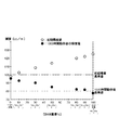
図1は、BAMのみからなる青色蛍光体層、CMSのみからなる青色蛍光体層及び実施例1乃至5の青色蛍光体層の初期輝度(○)及び1000時間動作後の輝度(●)をそれぞれ示すグラフである。 FIG. 1 shows the initial luminance (◯) and the luminance (●) after 1000 hours of operation of the blue phosphor layer consisting only of BAM, the blue phosphor layer consisting only of CMS, and the blue phosphor layer of Examples 1 to 5, respectively. It is a graph to show.
図1からも明らかであるように、青色蛍光体層の総重量に対するBAMの重量比が10乃至90%の範囲内であれば(この場合、CMSの重量比は90乃至10%の範囲内)、初期輝度及び輝度の経時変化の双方に関して、所望の特性を有する青色蛍光体層を得ることができることがわかる。 As is clear from FIG. 1, if the weight ratio of BAM to the total weight of the blue phosphor layer is in the range of 10 to 90% (in this case, the weight ratio of CMS is in the range of 90 to 10%). It can be seen that a blue phosphor layer having desired characteristics can be obtained with respect to both initial luminance and change with time of luminance.
上述の実施例1乃至5においては、第一の青色発光蛍光体としては、二価ユーロピウム付活アルミン酸塩系青色発光蛍光体に属するBaMgAl10O17:Eu2+(BAM)を選定し、第二の青色発光蛍光体としては、二価ユーロピウム付活ケイ酸塩系青色発光蛍光体に属するCaMgSi2O6:Eu2+(CMS)を選定した。すなわち、第一及び第二の青色発光蛍光体の双方について、それぞれ1種類の青色発光蛍光体を選定した。 In Examples 1 to 5 described above, as the first blue light emitting phosphor, BaMgAl 10 O 17 : Eu 2+ (BAM) belonging to the divalent europium activated aluminate blue light emitting phosphor is selected, As the second blue light emitting phosphor, CaMgSi 2 O 6 : Eu 2+ (CMS) belonging to the divalent europium activated silicate blue light emitting phosphor was selected. That is, one type of blue light-emitting phosphor was selected for each of the first and second blue light-emitting phosphors.
しかしながら、第一または第二の青色発光蛍光体として選定されるべき青色発光蛍光体は1種類の青色発光蛍光体に限定されるべきものではなく、2種類以上の青色発光蛍光体を選定することが可能である。 However, the blue-emitting phosphor to be selected as the first or second blue-emitting phosphor should not be limited to one type of blue-emitting phosphor, and two or more types of blue-emitting phosphors should be selected. Is possible.
その一例を実施例6として示す。 One example is shown as Example 6.
実施例6においては、第一の青色発光蛍光体としては、二価ユーロピウム付活アルミン酸塩系青色発光蛍光体に属するBaMgAl10O17:Eu2+及びBaMgAl14O23:Eu2+の2種類の青色発光蛍光体を選定し、第二の青色発光蛍光体としては、二価ユーロピウム付活ケイ酸塩系青色発光蛍光体に属するCaMgSi2O6:Eu2+(CMS)を選定した。 In Example 6, as the first blue light emitting phosphor, 2 of BaMgAl 10 O 17 : Eu 2+ and BaMgAl 14 O 23 : Eu 2+ belonging to the divalent europium activated aluminate-based blue light emitting phosphor. A kind of blue-emitting phosphor was selected, and as the second blue-emitting phosphor, CaMgSi 2 O 6 : Eu 2+ (CMS) belonging to a divalent europium-activated silicate-based blue-emitting phosphor was selected.
実施例1乃至5の場合と同様に、青色蛍光体層の全重量に対するBaMgAl10O17:Eu2+及びBaMgAl14O23:Eu2+の2種類の青色発光蛍光体の総重量比を100%、90%、80%、50%、30%、10%とした6種類のサンプル1−6を作製し、実施例1の場合と同様の測定を行った。 As in Examples 1 to 5, the total weight ratio of the two types of blue-emitting phosphors of BaMgAl 10 O 17 : Eu 2+ and BaMgAl 14 O 23 : Eu 2+ with respect to the total weight of the blue phosphor layer is 100. Six types of samples 1-6, which were%, 90%, 80%, 50%, 30%, and 10%, were produced, and the same measurement as in Example 1 was performed.
なお、サンプル1−6においては、BaMgAl10O17:Eu2+とBaMgAl14O23:Eu2+との重量比は60:40とした。 In Sample 1-6, the weight ratio of BaMgAl 10 O 17 : Eu 2+ to BaMgAl 14 O 23 : Eu 2+ was 60:40.
測定結果を表6に示す。 Table 6 shows the measurement results.
表6に示すように、BaMgAl10O17:Eu2+及びBaMgAl14O23:Eu2+の2種類の青色発光蛍光体からなる青色蛍光体層(サンプル1)の初期輝度は125であり、1000時間連続動作後の輝度は78である。すなわち、この青色蛍光体層の初期輝度は、必要とする輝度である100[cd/m2]に達しているが、1000時間連続動作後の輝度が、必要とする輝度である80[cd/m2]に達していない。 As shown in Table 6, the initial luminance of the blue phosphor layer (sample 1) composed of two kinds of blue light emitting phosphors of BaMgAl 10 O 17 : Eu 2+ and BaMgAl 14 O 23 : Eu 2+ is 125, The luminance after continuous operation for 1000 hours is 78. That is, the initial luminance of the blue phosphor layer has reached the required luminance of 100 [cd / m 2 ], but the luminance after 1000 hours of continuous operation is the required luminance of 80 [cd / m]. m 2 ] is not reached.
これに対して、BaMgAl10O17:Eu2+及びBaMgAl14O23:Eu2+の2種類の青色発光蛍光体を10乃至90重量%、CMSを10乃至90重量%の割合で混合した混合物からなるサンプル2乃至6に係る青色蛍光体層においては、初期輝度はそれぞれ122、120、113、107、102であり、1000時間連続動作後の輝度はそれぞれ81、82、85、90、93であった。すなわち、サンプル2乃至6の青色蛍光体層においては、いずれも、初期輝度が、必要とする輝度である100[cd/m2]に達しているとともに、1000時間連続動作後の輝度も、必要とする輝度である80[cd/m2]に達している。
In contrast, BaMgAl 10 O 17 : Eu 2+ and BaMgAl 14 O 23 : Eu 2+ are mixed in a proportion of 10 to 90% by weight and CMS in a proportion of 10 to 90% by weight. In the blue phosphor layers according to
このように、サンプル2乃至6の青色蛍光体層は、上述の実施例1乃至5に係る青色蛍光体層と同様に、初期輝度及び輝度の経時変化の双方に関して、所望の特性を有していることが判明した。
As described above, the blue phosphor layers of
このように、青色蛍光体層を構成する第一の青色発光蛍光体及び第二の青色発光蛍光体のうち、第一の青色発光蛍光体として、二価ユーロピウム付活アルミン酸塩系青色発光蛍光体に属する2種類以上の青色発光蛍光体を用いることが可能である。同様に、第二の青色発光蛍光体として、二価ユーロピウム付活ケイ酸塩系青色発光蛍光体に属する2種類以上の青色発光蛍光体を用いることも可能である。 Thus, among the first blue light-emitting phosphor and the second blue light-emitting phosphor constituting the blue phosphor layer, the first blue light-emitting phosphor is used as a divalent europium activated aluminate-based blue light-emitting fluorescence. Two or more kinds of blue-emitting phosphors belonging to the body can be used. Similarly, two or more kinds of blue light emitting phosphors belonging to the divalent europium activated silicate blue light emitting phosphor can be used as the second blue light emitting phosphor.
このように2種類以上の青色発光蛍光体を用いる場合には、それらの総重量の比率が青色蛍光体層の重量に対して10乃至90重量%になるように設定する。 When two or more kinds of blue light emitting phosphors are used as described above, the ratio of the total weight is set to 10 to 90% by weight with respect to the weight of the blue phosphor layer.
なお、実施例1乃至6においては、二価ユーロピウム付活アルミン酸塩系青色発光蛍光体に属する青色発光蛍光体として、BaMgAl10O17:Eu2+、BaMgAl12O19:Eu2+及びBaMgAl14O23:Eu2+の3つを用いたが、二価ユーロピウム付活アルミン酸塩系青色発光蛍光体に属する青色発光蛍光体はこの3つに限定されない。二価ユーロピウム付活アルミン酸塩系青色発光蛍光体に属する他の青色発光蛍光体を用いることもできる。 In Examples 1 to 6, BaMgAl 10 O 17 : Eu 2+ , BaMgAl 12 O 19 : Eu 2+ and BaMgAl are used as the blue-emitting phosphors belonging to the divalent europium activated aluminate-based blue-emitting phosphor. Although three of 14 O 23 : Eu 2+ were used, the blue-emitting phosphor belonging to the divalent europium-activated aluminate-based blue-emitting phosphor is not limited to these three. Other blue light emitting phosphors belonging to the divalent europium activated aluminate blue light emitting phosphor can also be used.
また、実施例1乃至6においては、二価ユーロピウム付活ケイ酸塩系青色発光蛍光体に属する青色発光蛍光体として、CaMgSi2O6:Eu2+(CMS)を用いたが、二価ユーロピウム付活ケイ酸塩系青色発光蛍光体に属する青色発光蛍光体はCMSには限定されない。例えば、CaSrMgSi2O6:Eu2+を用いることもできる。 In Examples 1 to 6, CaMgSi 2 O 6 : Eu 2+ (CMS) was used as the blue light emitting phosphor belonging to the divalent europium activated silicate blue light emitting phosphor. The blue light emitting phosphor belonging to the activated silicate blue light emitting phosphor is not limited to CMS. For example, CaSrMgSi 2 O 6 : Eu 2+ can be used.
上述の実施例1乃至6における青色蛍光体層はプラズマディスプレイパネルの一構成要素として、あるいは、プラズマ表示装置の一構成要素として提供される。 The blue phosphor layer in Examples 1 to 6 described above is provided as a component of the plasma display panel or as a component of the plasma display device.
本実施例においては、上述の実施例1乃至5及び実施例6のサンプル2乃至6に係る青色蛍光体層を使用したプラズマディスプレイパネルを備えるプラズマ表示装置の一例を示す。
In the present embodiment, an example of a plasma display device including a plasma display panel using the blue phosphor layer according to the
図3は、そのようなプラズマ表示装置10の構造を示すブロック図である。
FIG. 3 is a block diagram showing the structure of such a
図3に示すように、本実施例に係るプラズマ表示装置10は、アナログインターフェース20とプラズマディスプレイモジュール30とからなる。
As shown in FIG. 3, the
アナログインターフェース20は、クロマ・デコーダを備えるY/C分離回路21と、アナログ・ディジタル(A/D)変換回路22と、PLL(Phase Locked Loop)回路を備える同期信号制御回路23と、画像フォーマット変換回路24と、逆γ変換回路25と、システム・コントロール回路26と、PLE制御回路27と、から構成されている。
The
概略的には、アナログインターフェース20は、受信したアナログ映像信号をディジタル映像信号に変換した後、そのディジタル映像信号をプラズマディスプレイモジュール30に供給する。
Schematically, the
例えば、テレビチューナーから発信されたアナログ映像信号はY/C分離回路21においてRGBの各色の輝度信号に分解された後、A/D変換回路22においてディジタル信号に変換される。
For example, an analog video signal transmitted from a TV tuner is decomposed into RGB luminance signals in the Y /
その後、プラズマディスプレイモジュール30の画素構成と映像信号の画素構成が異なる場合には、画像フォーマット変換回路24で必要な変換が行われる。
Thereafter, when the pixel configuration of the
プラズマディスプレイパネルの入力信号に対する表示輝度の特性は線形的に比例するが、通常の映像信号はCRTの特性に合わせて、予め補正(γ変換)されている。このため、A/D変換回路22において映像信号のA/D変換を行った後、逆γ変換回路25において、映像信号に対して逆γ変換を施し、線形特性に復元されたディジタル映像信号を生成する。このディジタル映像信号はRGB映像信号としてプラズマディスプレイモジュール30に出力される。
The display luminance characteristic with respect to the input signal of the plasma display panel is linearly proportional, but a normal video signal is corrected (γ-converted) in advance in accordance with the CRT characteristic. For this reason, after the A / D conversion of the video signal is performed in the A / D conversion circuit 22, the inverse γ conversion circuit 25 performs the inverse γ conversion on the video signal, and the digital video signal restored to the linear characteristic is obtained. Generate. This digital video signal is output to the
アナログ映像信号には、A/D変換用のサンプリングクロック及びデータクロック信号が含まれていないため、同期信号制御回路23に内蔵されているPLL回路が、アナログ映像信号と同時に供給される水平同期信号を基準として、サンプリングクロック及びデータクロック信号を生成し、プラズマディスプレイモジュール30に出力する。
Since the analog video signal does not include the sampling clock and data clock signal for A / D conversion, the PLL circuit built in the synchronization
PLE制御回路27は輝度制御を行う。具体的には、平均輝度レベルが所定値以下である場合には表示輝度を上昇させ、平均輝度レベルが所定値を超える場合には表示輝度を制限する。
The
システム・コントロール回路26は、各種制御信号をプラズマディスプレイモジュール30に対して出力する。
The system control circuit 26 outputs various control signals to the
プラズマディスプレイモジュール30は、ディジタル信号処理・制御回路31と、パネル部32と、DC/DCコンバータを内蔵するモジュール内電源回路33と、から構成されている。
The
ディジタル信号処理・制御回路31は、入力インターフェース信号処理回路34と、フレームメモリ35と、メモリ制御回路36と、ドライバ制御回路37と、から構成されている。
The digital signal processing /
入力インターフェース信号処理回路34は、システム・コントロール回路26から発信される各種制御信号、逆γ変換回路25から発信されるRGB映像信号、同期信号制御回路23から発信される同期信号、PLL回路から発信されるデータクロック信号を受信する。
The input interface
例えば、入力インターフェース信号処理回路34に入力された映像信号の平均輝度レベルは入力インターフェース信号処理回路34内の入力信号平均輝度レベル演算回路(図示せず)により計算され、例えば、5ビットデータとして出力される。また、PLE制御回路27は、平均輝度レベルに応じてPLE制御データを設定し、入力インターフェース信号処理回路34内の輝度レベル制御回路(図示せず)に入力する。
For example, the average luminance level of the video signal input to the input interface
ディジタル信号処理・制御回路31は、入力インターフェース信号処理回路34において、これらの各種信号を処理した後、制御信号をパネル部32に送信する。
The digital signal processing /
パネル部32は、プラズマディスプレイパネル50と、走査電極を駆動する走査ドライバ38と、データ電極を駆動するデータドライバ39と、プラズマディスプレイパネル50及び走査ドライバ38にパルス電圧を供給する高圧パルス回路40と、高圧パルス回路40からの余剰電力を回収する電力回収回路41と、から構成されている。
The
プラズマディスプレイパネル50は、上述の実施例1乃至5及び実施例6のサンプル2乃至6に係る青色蛍光体層を備えている。
The
プラズマディスプレイパネル50においては、走査ドライバ38が走査電極を制御し、データドライバ39がデータ電極を制御することにより、所定の表示セルの点灯または非点灯が制御され、所望の画像の表示が行われる。
In the
なお、ロジック用電源がディジタル信号処理・制御回路31及びパネル部32にロジック用電力を供給している。さらに、モジュール内電源回路33は、表示用電源から直流電力を供給され、この直流電力の電圧を所定の電圧に変換した後、パネル部32に供給している。
The logic power supply supplies logic power to the digital signal processing /
本実施例に係るプラズマ表示装置10は、上述の実施例1乃至5及び実施例6のサンプル2乃至6に係る青色蛍光体層を備えるプラズマディスプレイパネル50を有しているため、青色発光に関して、初期輝度を大きく低下させることなく、輝度の経時変化を抑制することが可能である。
Since the
10 プラズマ表示装置
20 アナログインターフェース
21 Y/C分離回路
22 アナログ・ディジタル(A/D)変換回路
23 同期信号制御回路
24 画像フォーマット変換回路
25 逆γ変換回路
26 システム・コントロール回路
27 PLE制御回路
30 プラズマディスプレイモジュール
31 ディジタル信号処理・制御回路
32 パネル部
33 モジュール内電源回路
300 プラズマディスプレイパネル
351 前面基板
352 背面基板
301、302 絶縁基板
303 走査電極
304 共通電極
305、306 トレース電極
311 蛍光体層
312 誘電体層
313 保護層
307 データ電極
314 誘電体層
315 隔壁
DESCRIPTION OF
Claims (11)
前記第一基板は、
透明基板と、
前記透明基板上において前記第二基板に対向して形成された走査電極及び共通電極と、
前記透明基板、前記走査電極及び前記共通電極を覆って形成された誘電体層と、
からなり、
前記第二基板は、
絶縁性基板と、
前記絶縁性基板上に形成された複数のデータ電極と、
前記絶縁性基板上に形成された複数の隔壁と、
相互に隣接する前記隔壁の間において前記絶縁性基板及び前記データ電極を覆って形成された蛍光体層と、
からなり、
前記蛍光体層は少なくとも青色発光蛍光体からなる青色蛍光体層を含み、
前記青色蛍光体層は、初期輝度及び輝度の経時変化の双方が相互に異なる2種類以上の青色発光蛍光体の混合物からなるものであるプラズマディスプレイパネル。 A plasma display panel comprising a display-side first substrate and a second substrate disposed opposite to the first substrate,
The first substrate is
A transparent substrate;
A scanning electrode and a common electrode formed on the transparent substrate so as to face the second substrate;
A dielectric layer formed to cover the transparent substrate, the scan electrode and the common electrode;
Consists of
The second substrate is
An insulating substrate;
A plurality of data electrodes formed on the insulating substrate;
A plurality of partition walls formed on the insulating substrate;
A phosphor layer formed to cover the insulating substrate and the data electrode between the barrier ribs adjacent to each other;
Consists of
The phosphor layer includes a blue phosphor layer made of at least a blue-emitting phosphor,
The blue phosphor layer is a plasma display panel made of a mixture of two or more types of blue light emitting phosphors that are different from each other in both initial luminance and luminance with time.
請求項1乃至9のいずれか一項に記載のプラズマディスプレイパネルを含み、前記アナログインターフェースから受信した前記ディジタル映像信号に応じた映像を出力するプラズマディスプレイモジュールと、
からなるプラズマ表示装置。
An analog interface that converts the received analog video signal into a digital video signal and outputs the digital video signal;
A plasma display module comprising the plasma display panel according to any one of claims 1 to 9, wherein the plasma display module outputs an image corresponding to the digital image signal received from the analog interface;
A plasma display device comprising:
Priority Applications (2)
| Application Number | Priority Date | Filing Date | Title |
|---|---|---|---|
| JP2003349749A JP2005116363A (en) | 2003-10-08 | 2003-10-08 | Plasma display panel |
| US10/934,548 US7239085B2 (en) | 2003-10-08 | 2004-09-07 | Plasma display panel |
Applications Claiming Priority (1)
| Application Number | Priority Date | Filing Date | Title |
|---|---|---|---|
| JP2003349749A JP2005116363A (en) | 2003-10-08 | 2003-10-08 | Plasma display panel |
Publications (2)
| Publication Number | Publication Date |
|---|---|
| JP2005116363A true JP2005116363A (en) | 2005-04-28 |
| JP2005116363A5 JP2005116363A5 (en) | 2006-11-09 |
Family
ID=34419714
Family Applications (1)
| Application Number | Title | Priority Date | Filing Date |
|---|---|---|---|
| JP2003349749A Pending JP2005116363A (en) | 2003-10-08 | 2003-10-08 | Plasma display panel |
Country Status (2)
| Country | Link |
|---|---|
| US (1) | US7239085B2 (en) |
| JP (1) | JP2005116363A (en) |
Cited By (2)
| Publication number | Priority date | Publication date | Assignee | Title |
|---|---|---|---|---|
| WO2007013515A1 (en) * | 2005-07-27 | 2007-02-01 | Matsushita Electric Industrial Co., Ltd. | Gas discharge light emitting panel |
| WO2010061419A1 (en) * | 2008-11-25 | 2010-06-03 | 日立プラズマディスプレイ株式会社 | Plasma display panel |
Families Citing this family (32)
| Publication number | Priority date | Publication date | Assignee | Title |
|---|---|---|---|---|
| US7005679B2 (en) | 2003-05-01 | 2006-02-28 | Cree, Inc. | Multiple component solid state white light |
| EP1683849A4 (en) * | 2003-10-21 | 2009-04-15 | Sumitomo Chemical Co | Fluorescent material and fluorescent material paste |
| KR100708649B1 (en) * | 2004-11-10 | 2007-04-17 | 삼성에스디아이 주식회사 | Plasma Display Panel |
| US8125137B2 (en) | 2005-01-10 | 2012-02-28 | Cree, Inc. | Multi-chip light emitting device lamps for providing high-CRI warm white light and light fixtures including the same |
| US7564180B2 (en) * | 2005-01-10 | 2009-07-21 | Cree, Inc. | Light emission device and method utilizing multiple emitters and multiple phosphors |
| KR101332139B1 (en) | 2005-12-21 | 2013-11-21 | 크리, 인코포레이티드 | Lighting device and lighting method |
| CN101460779A (en) | 2005-12-21 | 2009-06-17 | 科锐Led照明技术公司 | Lighting device |
| TWI396814B (en) | 2005-12-22 | 2013-05-21 | 克里公司 | Lighting device |
| KR100670385B1 (en) * | 2006-02-23 | 2007-01-16 | 삼성에스디아이 주식회사 | A phosphor, a phosphor paste composition comprising the phosphor and a flat display device employing a phosphor layer comprising the phosphor |
| US8513875B2 (en) | 2006-04-18 | 2013-08-20 | Cree, Inc. | Lighting device and lighting method |
| US9084328B2 (en) | 2006-12-01 | 2015-07-14 | Cree, Inc. | Lighting device and lighting method |
| KR101419954B1 (en) | 2006-04-18 | 2014-07-16 | 크리, 인코포레이티드 | Lighting device and lighting method |
| BRPI0710461A2 (en) | 2006-04-20 | 2011-08-16 | Cree Led Lighting Solutions | lighting device and lighting method |
| KR20090019871A (en) | 2006-05-31 | 2009-02-25 | 크리 엘이디 라이팅 솔루션즈, 인크. | Lighting device and method of lighting |
| JP2008050523A (en) * | 2006-08-28 | 2008-03-06 | Hitachi Ltd | Plasma display device and light-emitting device |
| US8029155B2 (en) | 2006-11-07 | 2011-10-04 | Cree, Inc. | Lighting device and lighting method |
| US9441793B2 (en) | 2006-12-01 | 2016-09-13 | Cree, Inc. | High efficiency lighting device including one or more solid state light emitters, and method of lighting |
| US7918581B2 (en) | 2006-12-07 | 2011-04-05 | Cree, Inc. | Lighting device and lighting method |
| EP2122231B1 (en) * | 2007-02-22 | 2014-10-01 | Cree, Inc. | Lighting devices, methods of lighting, light filters and methods of filtering light |
| WO2008137975A1 (en) | 2007-05-08 | 2008-11-13 | Cree Led Lighting Solutions, Inc. | Lighting device and lighting method |
| JP2010527510A (en) | 2007-05-08 | 2010-08-12 | クリー エル イー ディー ライティング ソリューションズ インコーポレイテッド | Lighting device and lighting method |
| KR20100020464A (en) | 2007-05-08 | 2010-02-22 | 크리 엘이디 라이팅 솔루션즈, 인크. | Lighting device and lighting method |
| EP2156090B1 (en) | 2007-05-08 | 2016-07-06 | Cree, Inc. | Lighting device and lighting method |
| JP2010527156A (en) | 2007-05-08 | 2010-08-05 | クリー エル イー ディー ライティング ソリューションズ インコーポレイテッド | Lighting device and lighting method |
| US7863635B2 (en) | 2007-08-07 | 2011-01-04 | Cree, Inc. | Semiconductor light emitting devices with applied wavelength conversion materials |
| WO2009049019A1 (en) | 2007-10-10 | 2009-04-16 | Cree Led Lighting Solutions, Inc. | Lighting device and method of making |
| US8240875B2 (en) | 2008-06-25 | 2012-08-14 | Cree, Inc. | Solid state linear array modules for general illumination |
| US8921876B2 (en) | 2009-06-02 | 2014-12-30 | Cree, Inc. | Lighting devices with discrete lumiphor-bearing regions within or on a surface of remote elements |
| CN102630288B (en) | 2009-09-25 | 2015-09-09 | 科锐公司 | There is the lighting apparatus of low dazzle and high brightness levels uniformity |
| US9275979B2 (en) | 2010-03-03 | 2016-03-01 | Cree, Inc. | Enhanced color rendering index emitter through phosphor separation |
| US11251164B2 (en) | 2011-02-16 | 2022-02-15 | Creeled, Inc. | Multi-layer conversion material for down conversion in solid state lighting |
| CN104241262B (en) | 2013-06-14 | 2020-11-06 | 惠州科锐半导体照明有限公司 | Light emitting device and display device |
Family Cites Families (3)
| Publication number | Priority date | Publication date | Assignee | Title |
|---|---|---|---|---|
| JP2001084911A (en) | 1999-09-14 | 2001-03-30 | Mitsubishi Electric Corp | Plasma display device |
| JP3985478B2 (en) | 2000-09-29 | 2007-10-03 | 住友化学株式会社 | Phosphor for vacuum ultraviolet light-excited light emitting device |
| DE10061720A1 (en) * | 2000-12-12 | 2002-06-13 | Philips Corp Intellectual Pty | Plasma screen comprises front plate, carrier plate with phosphor layer, rib structure which divides chamber between front plate and carrier plate into plasma cells which are filled with gas, and electrode arrays |
-
2003
- 2003-10-08 JP JP2003349749A patent/JP2005116363A/en active Pending
-
2004
- 2004-09-07 US US10/934,548 patent/US7239085B2/en not_active Expired - Fee Related
Cited By (3)
| Publication number | Priority date | Publication date | Assignee | Title |
|---|---|---|---|---|
| WO2007013515A1 (en) * | 2005-07-27 | 2007-02-01 | Matsushita Electric Industrial Co., Ltd. | Gas discharge light emitting panel |
| WO2010061419A1 (en) * | 2008-11-25 | 2010-06-03 | 日立プラズマディスプレイ株式会社 | Plasma display panel |
| JPWO2010061419A1 (en) * | 2008-11-25 | 2012-04-19 | 日立プラズマディスプレイ株式会社 | Plasma display panel |
Also Published As
| Publication number | Publication date |
|---|---|
| US7239085B2 (en) | 2007-07-03 |
| US20050077810A1 (en) | 2005-04-14 |
Similar Documents
| Publication | Publication Date | Title |
|---|---|---|
| JP2005116363A (en) | Plasma display panel | |
| US7138965B2 (en) | Plasma display device, luminescent device and image and information display system using the same | |
| KR101005369B1 (en) | Plasma display device | |
| JP2008050523A (en) | Plasma display device and light-emitting device | |
| JP2007103052A (en) | Plasma display panel | |
| US8129905B2 (en) | Phosphor and light emitting device using the phosphor | |
| JP2003142005A (en) | Plasma display device and image display system using the same | |
| US8410677B2 (en) | Blue phosphor, light-emitting device, and plasma display panel | |
| JP2001135239A (en) | Plasma display unit and picture image display system using the same | |
| JP5094246B2 (en) | Plasma display device | |
| US20090224668A1 (en) | Plasma display device | |
| JP5564146B2 (en) | Plasma display panel and phosphor | |
| JP2005002234A (en) | Plasma display and phosphor for plasma display | |
| JP2009259462A (en) | Plasma display panel | |
| JP2010177072A (en) | Plasma display panel | |
| JP2001229835A (en) | Plasma display panel | |
| JPWO2007013515A1 (en) | Gas discharge light emitting panel | |
| JP2005032721A (en) | Spontaneous light emission type color display device, and driving method of the same | |
| JP2008262927A (en) | Plasma display unit and video display system using it | |
| JP2010097861A (en) | Display device and plasma display panel | |
| JP2011216474A (en) | Plasma display device | |
| JP2010177073A (en) | Plasma display panel | |
| JP2009295407A (en) | Image display apparatus | |
| JP2009224032A (en) | Display device and plasma display panel | |
| JP2010080283A (en) | Plasma display panel |
Legal Events
| Date | Code | Title | Description |
|---|---|---|---|
| RD02 | Notification of acceptance of power of attorney |
Free format text: JAPANESE INTERMEDIATE CODE: A7422 Effective date: 20050407 |
|
| A711 | Notification of change in applicant |
Free format text: JAPANESE INTERMEDIATE CODE: A711 Effective date: 20050328 |
|
| A521 | Request for written amendment filed |
Free format text: JAPANESE INTERMEDIATE CODE: A523 Effective date: 20060926 |
|
| A621 | Written request for application examination |
Free format text: JAPANESE INTERMEDIATE CODE: A621 Effective date: 20060926 |
|
| A977 | Report on retrieval |
Free format text: JAPANESE INTERMEDIATE CODE: A971007 Effective date: 20080728 |
|
| A131 | Notification of reasons for refusal |
Free format text: JAPANESE INTERMEDIATE CODE: A131 Effective date: 20081031 |
|
| A02 | Decision of refusal |
Free format text: JAPANESE INTERMEDIATE CODE: A02 Effective date: 20090313 |