JP2005109501A - Bipolar transistor with selectively deposited emitter - Google Patents
Bipolar transistor with selectively deposited emitter Download PDFInfo
- Publication number
- JP2005109501A JP2005109501A JP2004283339A JP2004283339A JP2005109501A JP 2005109501 A JP2005109501 A JP 2005109501A JP 2004283339 A JP2004283339 A JP 2004283339A JP 2004283339 A JP2004283339 A JP 2004283339A JP 2005109501 A JP2005109501 A JP 2005109501A
- Authority
- JP
- Japan
- Prior art keywords
- emitter
- forming
- opening
- bipolar junction
- junction transistor
- Prior art date
- Legal status (The legal status is an assumption and is not a legal conclusion. Google has not performed a legal analysis and makes no representation as to the accuracy of the status listed.)
- Pending
Links
- 238000000034 method Methods 0.000 claims abstract description 92
- 229910021420 polycrystalline silicon Inorganic materials 0.000 claims abstract description 46
- 238000000151 deposition Methods 0.000 claims abstract description 27
- 230000008021 deposition Effects 0.000 claims abstract description 16
- 238000011065 in-situ storage Methods 0.000 claims abstract description 7
- VYPSYNLAJGMNEJ-UHFFFAOYSA-N Silicium dioxide Chemical compound O=[Si]=O VYPSYNLAJGMNEJ-UHFFFAOYSA-N 0.000 claims description 50
- 239000000758 substrate Substances 0.000 claims description 41
- 239000000377 silicon dioxide Substances 0.000 claims description 25
- 235000012239 silicon dioxide Nutrition 0.000 claims description 25
- 239000004065 semiconductor Substances 0.000 claims description 20
- 229910052581 Si3N4 Inorganic materials 0.000 claims description 18
- 239000002019 doping agent Substances 0.000 claims description 18
- 238000002513 implantation Methods 0.000 claims description 18
- 239000000463 material Substances 0.000 claims description 18
- HQVNEWCFYHHQES-UHFFFAOYSA-N silicon nitride Chemical compound N12[Si]34N5[Si]62N3[Si]51N64 HQVNEWCFYHHQES-UHFFFAOYSA-N 0.000 claims description 16
- 125000006850 spacer group Chemical group 0.000 claims description 16
- 238000005530 etching Methods 0.000 claims description 9
- 238000005137 deposition process Methods 0.000 claims description 7
- 238000000059 patterning Methods 0.000 claims description 6
- 239000002210 silicon-based material Substances 0.000 claims description 2
- 229910021421 monocrystalline silicon Inorganic materials 0.000 claims 3
- XUIMIQQOPSSXEZ-UHFFFAOYSA-N Silicon Chemical compound [Si] XUIMIQQOPSSXEZ-UHFFFAOYSA-N 0.000 abstract description 24
- 229910052710 silicon Inorganic materials 0.000 abstract description 24
- 239000010703 silicon Substances 0.000 abstract description 24
- 229910052751 metal Inorganic materials 0.000 abstract description 2
- 239000002184 metal Substances 0.000 abstract description 2
- 239000003989 dielectric material Substances 0.000 abstract 1
- 238000003475 lamination Methods 0.000 abstract 1
- 239000010410 layer Substances 0.000 description 95
- 230000005669 field effect Effects 0.000 description 16
- 229910044991 metal oxide Inorganic materials 0.000 description 16
- 150000004706 metal oxides Chemical class 0.000 description 16
- VEXZGXHMUGYJMC-UHFFFAOYSA-N Hydrochloric acid Chemical compound Cl VEXZGXHMUGYJMC-UHFFFAOYSA-N 0.000 description 12
- BOTDANWDWHJENH-UHFFFAOYSA-N Tetraethyl orthosilicate Chemical compound CCO[Si](OCC)(OCC)OCC BOTDANWDWHJENH-UHFFFAOYSA-N 0.000 description 11
- 229920002120 photoresistant polymer Polymers 0.000 description 10
- 229920005591 polysilicon Polymers 0.000 description 6
- 230000003647 oxidation Effects 0.000 description 5
- 238000007254 oxidation reaction Methods 0.000 description 5
- 229910052785 arsenic Inorganic materials 0.000 description 4
- RQNWIZPPADIBDY-UHFFFAOYSA-N arsenic atom Chemical compound [As] RQNWIZPPADIBDY-UHFFFAOYSA-N 0.000 description 4
- 239000007943 implant Substances 0.000 description 4
- 238000001465 metallisation Methods 0.000 description 4
- 230000008901 benefit Effects 0.000 description 3
- 230000015572 biosynthetic process Effects 0.000 description 3
- 239000013078 crystal Substances 0.000 description 3
- 230000000873 masking effect Effects 0.000 description 3
- 239000011800 void material Substances 0.000 description 3
- ZOXJGFHDIHLPTG-UHFFFAOYSA-N Boron Chemical compound [B] ZOXJGFHDIHLPTG-UHFFFAOYSA-N 0.000 description 2
- 229910021417 amorphous silicon Inorganic materials 0.000 description 2
- 230000000295 complement effect Effects 0.000 description 2
- 239000012535 impurity Substances 0.000 description 2
- 230000000977 initiatory effect Effects 0.000 description 2
- WQJQOUPTWCFRMM-UHFFFAOYSA-N tungsten disilicide Chemical compound [Si]#[W]#[Si] WQJQOUPTWCFRMM-UHFFFAOYSA-N 0.000 description 2
- 229910021342 tungsten silicide Inorganic materials 0.000 description 2
- 229910000577 Silicon-germanium Inorganic materials 0.000 description 1
- LEVVHYCKPQWKOP-UHFFFAOYSA-N [Si].[Ge] Chemical compound [Si].[Ge] LEVVHYCKPQWKOP-UHFFFAOYSA-N 0.000 description 1
- 229910052796 boron Inorganic materials 0.000 description 1
- 230000015556 catabolic process Effects 0.000 description 1
- 238000004140 cleaning Methods 0.000 description 1
- 230000002517 constrictor effect Effects 0.000 description 1
- 238000006731 degradation reaction Methods 0.000 description 1
- NTPSYCFWEYOKTG-UHFFFAOYSA-N dioxosilane;tetraethyl silicate Chemical compound O=[Si]=O.CCO[Si](OCC)(OCC)OCC NTPSYCFWEYOKTG-UHFFFAOYSA-N 0.000 description 1
- 238000009413 insulation Methods 0.000 description 1
- 238000004519 manufacturing process Methods 0.000 description 1
- 230000001590 oxidative effect Effects 0.000 description 1
- 239000002356 single layer Substances 0.000 description 1
- 238000001039 wet etching Methods 0.000 description 1
Images


Classifications
-
- H—ELECTRICITY
- H01—ELECTRIC ELEMENTS
- H01L—SEMICONDUCTOR DEVICES NOT COVERED BY CLASS H10
- H01L27/00—Devices consisting of a plurality of semiconductor or other solid-state components formed in or on a common substrate
- H01L27/02—Devices consisting of a plurality of semiconductor or other solid-state components formed in or on a common substrate including semiconductor components specially adapted for rectifying, oscillating, amplifying or switching and having potential barriers; including integrated passive circuit elements having potential barriers
- H01L27/04—Devices consisting of a plurality of semiconductor or other solid-state components formed in or on a common substrate including semiconductor components specially adapted for rectifying, oscillating, amplifying or switching and having potential barriers; including integrated passive circuit elements having potential barriers the substrate being a semiconductor body
- H01L27/06—Devices consisting of a plurality of semiconductor or other solid-state components formed in or on a common substrate including semiconductor components specially adapted for rectifying, oscillating, amplifying or switching and having potential barriers; including integrated passive circuit elements having potential barriers the substrate being a semiconductor body including a plurality of individual components in a non-repetitive configuration
- H01L27/0611—Devices consisting of a plurality of semiconductor or other solid-state components formed in or on a common substrate including semiconductor components specially adapted for rectifying, oscillating, amplifying or switching and having potential barriers; including integrated passive circuit elements having potential barriers the substrate being a semiconductor body including a plurality of individual components in a non-repetitive configuration integrated circuits having a two-dimensional layout of components without a common active region
- H01L27/0617—Devices consisting of a plurality of semiconductor or other solid-state components formed in or on a common substrate including semiconductor components specially adapted for rectifying, oscillating, amplifying or switching and having potential barriers; including integrated passive circuit elements having potential barriers the substrate being a semiconductor body including a plurality of individual components in a non-repetitive configuration integrated circuits having a two-dimensional layout of components without a common active region comprising components of the field-effect type
- H01L27/0623—Devices consisting of a plurality of semiconductor or other solid-state components formed in or on a common substrate including semiconductor components specially adapted for rectifying, oscillating, amplifying or switching and having potential barriers; including integrated passive circuit elements having potential barriers the substrate being a semiconductor body including a plurality of individual components in a non-repetitive configuration integrated circuits having a two-dimensional layout of components without a common active region comprising components of the field-effect type in combination with bipolar transistors
-
- H—ELECTRICITY
- H01—ELECTRIC ELEMENTS
- H01L—SEMICONDUCTOR DEVICES NOT COVERED BY CLASS H10
- H01L29/00—Semiconductor devices specially adapted for rectifying, amplifying, oscillating or switching and having potential barriers; Capacitors or resistors having potential barriers, e.g. a PN-junction depletion layer or carrier concentration layer; Details of semiconductor bodies or of electrodes thereof ; Multistep manufacturing processes therefor
- H01L29/66—Types of semiconductor device ; Multistep manufacturing processes therefor
- H01L29/68—Types of semiconductor device ; Multistep manufacturing processes therefor controllable by only the electric current supplied, or only the electric potential applied, to an electrode which does not carry the current to be rectified, amplified or switched
- H01L29/70—Bipolar devices
- H01L29/72—Transistor-type devices, i.e. able to continuously respond to applied control signals
- H01L29/73—Bipolar junction transistors
-
- H—ELECTRICITY
- H01—ELECTRIC ELEMENTS
- H01L—SEMICONDUCTOR DEVICES NOT COVERED BY CLASS H10
- H01L21/00—Processes or apparatus adapted for the manufacture or treatment of semiconductor or solid state devices or of parts thereof
- H01L21/70—Manufacture or treatment of devices consisting of a plurality of solid state components formed in or on a common substrate or of parts thereof; Manufacture of integrated circuit devices or of parts thereof
- H01L21/77—Manufacture or treatment of devices consisting of a plurality of solid state components or integrated circuits formed in, or on, a common substrate
- H01L21/78—Manufacture or treatment of devices consisting of a plurality of solid state components or integrated circuits formed in, or on, a common substrate with subsequent division of the substrate into plural individual devices
- H01L21/82—Manufacture or treatment of devices consisting of a plurality of solid state components or integrated circuits formed in, or on, a common substrate with subsequent division of the substrate into plural individual devices to produce devices, e.g. integrated circuits, each consisting of a plurality of components
- H01L21/822—Manufacture or treatment of devices consisting of a plurality of solid state components or integrated circuits formed in, or on, a common substrate with subsequent division of the substrate into plural individual devices to produce devices, e.g. integrated circuits, each consisting of a plurality of components the substrate being a semiconductor, using silicon technology
- H01L21/8248—Combination of bipolar and field-effect technology
- H01L21/8249—Bipolar and MOS technology
-
- H—ELECTRICITY
- H01—ELECTRIC ELEMENTS
- H01L—SEMICONDUCTOR DEVICES NOT COVERED BY CLASS H10
- H01L29/00—Semiconductor devices specially adapted for rectifying, amplifying, oscillating or switching and having potential barriers; Capacitors or resistors having potential barriers, e.g. a PN-junction depletion layer or carrier concentration layer; Details of semiconductor bodies or of electrodes thereof ; Multistep manufacturing processes therefor
- H01L29/02—Semiconductor bodies ; Multistep manufacturing processes therefor
- H01L29/06—Semiconductor bodies ; Multistep manufacturing processes therefor characterised by their shape; characterised by the shapes, relative sizes, or dispositions of the semiconductor regions ; characterised by the concentration or distribution of impurities within semiconductor regions
- H01L29/08—Semiconductor bodies ; Multistep manufacturing processes therefor characterised by their shape; characterised by the shapes, relative sizes, or dispositions of the semiconductor regions ; characterised by the concentration or distribution of impurities within semiconductor regions with semiconductor regions connected to an electrode carrying current to be rectified, amplified or switched and such electrode being part of a semiconductor device which comprises three or more electrodes
- H01L29/0804—Emitter regions of bipolar transistors
-
- H—ELECTRICITY
- H01—ELECTRIC ELEMENTS
- H01L—SEMICONDUCTOR DEVICES NOT COVERED BY CLASS H10
- H01L29/00—Semiconductor devices specially adapted for rectifying, amplifying, oscillating or switching and having potential barriers; Capacitors or resistors having potential barriers, e.g. a PN-junction depletion layer or carrier concentration layer; Details of semiconductor bodies or of electrodes thereof ; Multistep manufacturing processes therefor
- H01L29/66—Types of semiconductor device ; Multistep manufacturing processes therefor
- H01L29/66007—Multistep manufacturing processes
- H01L29/66075—Multistep manufacturing processes of devices having semiconductor bodies comprising group 14 or group 13/15 materials
- H01L29/66227—Multistep manufacturing processes of devices having semiconductor bodies comprising group 14 or group 13/15 materials the devices being controllable only by the electric current supplied or the electric potential applied, to an electrode which does not carry the current to be rectified, amplified or switched, e.g. three-terminal devices
- H01L29/66234—Bipolar junction transistors [BJT]
- H01L29/66242—Heterojunction transistors [HBT]
-
- H—ELECTRICITY
- H01—ELECTRIC ELEMENTS
- H01L—SEMICONDUCTOR DEVICES NOT COVERED BY CLASS H10
- H01L29/00—Semiconductor devices specially adapted for rectifying, amplifying, oscillating or switching and having potential barriers; Capacitors or resistors having potential barriers, e.g. a PN-junction depletion layer or carrier concentration layer; Details of semiconductor bodies or of electrodes thereof ; Multistep manufacturing processes therefor
- H01L29/66—Types of semiconductor device ; Multistep manufacturing processes therefor
- H01L29/66007—Multistep manufacturing processes
- H01L29/66075—Multistep manufacturing processes of devices having semiconductor bodies comprising group 14 or group 13/15 materials
- H01L29/66227—Multistep manufacturing processes of devices having semiconductor bodies comprising group 14 or group 13/15 materials the devices being controllable only by the electric current supplied or the electric potential applied, to an electrode which does not carry the current to be rectified, amplified or switched, e.g. three-terminal devices
- H01L29/66234—Bipolar junction transistors [BJT]
- H01L29/66272—Silicon vertical transistors
- H01L29/66287—Silicon vertical transistors with a single crystalline emitter, collector or base including extrinsic, link or graft base formed on the silicon substrate, e.g. by epitaxy, recrystallisation, after insulating device isolation
-
- H—ELECTRICITY
- H01—ELECTRIC ELEMENTS
- H01L—SEMICONDUCTOR DEVICES NOT COVERED BY CLASS H10
- H01L29/00—Semiconductor devices specially adapted for rectifying, amplifying, oscillating or switching and having potential barriers; Capacitors or resistors having potential barriers, e.g. a PN-junction depletion layer or carrier concentration layer; Details of semiconductor bodies or of electrodes thereof ; Multistep manufacturing processes therefor
- H01L29/66—Types of semiconductor device ; Multistep manufacturing processes therefor
- H01L29/68—Types of semiconductor device ; Multistep manufacturing processes therefor controllable by only the electric current supplied, or only the electric potential applied, to an electrode which does not carry the current to be rectified, amplified or switched
- H01L29/70—Bipolar devices
- H01L29/72—Transistor-type devices, i.e. able to continuously respond to applied control signals
- H01L29/73—Bipolar junction transistors
- H01L29/732—Vertical transistors
- H01L29/7322—Vertical transistors having emitter-base and base-collector junctions leaving at the same surface of the body, e.g. planar transistor
-
- H—ELECTRICITY
- H01—ELECTRIC ELEMENTS
- H01L—SEMICONDUCTOR DEVICES NOT COVERED BY CLASS H10
- H01L29/00—Semiconductor devices specially adapted for rectifying, amplifying, oscillating or switching and having potential barriers; Capacitors or resistors having potential barriers, e.g. a PN-junction depletion layer or carrier concentration layer; Details of semiconductor bodies or of electrodes thereof ; Multistep manufacturing processes therefor
- H01L29/66—Types of semiconductor device ; Multistep manufacturing processes therefor
- H01L29/68—Types of semiconductor device ; Multistep manufacturing processes therefor controllable by only the electric current supplied, or only the electric potential applied, to an electrode which does not carry the current to be rectified, amplified or switched
- H01L29/70—Bipolar devices
- H01L29/72—Transistor-type devices, i.e. able to continuously respond to applied control signals
- H01L29/73—Bipolar junction transistors
- H01L29/737—Hetero-junction transistors
- H01L29/7371—Vertical transistors
- H01L29/7378—Vertical transistors comprising lattice mismatched active layers, e.g. SiGe strained layer transistors
Landscapes
- Engineering & Computer Science (AREA)
- Power Engineering (AREA)
- Microelectronics & Electronic Packaging (AREA)
- Condensed Matter Physics & Semiconductors (AREA)
- General Physics & Mathematics (AREA)
- Physics & Mathematics (AREA)
- Computer Hardware Design (AREA)
- Ceramic Engineering (AREA)
- Manufacturing & Machinery (AREA)
- Bipolar Transistors (AREA)
- Metal-Oxide And Bipolar Metal-Oxide Semiconductor Integrated Circuits (AREA)
- Bipolar Integrated Circuits (AREA)
- Electrodes Of Semiconductors (AREA)
Abstract
Description
本発明は全体としてバイポーラトランジスタに関し、具体的にはバイポーラトランジスタのエミッタ領域を形成する方法、およびこのような方法によって形成されたトランジスタに関する。 The present invention relates generally to bipolar transistors, and more specifically to a method of forming an emitter region of a bipolar transistor and a transistor formed by such a method.
本発明は2003年9月30日に出願された仮特許出願第60/507,374号、「選択的に蒸着されたエミッタを有するバイポーラトランジスタ」(Bipolar Transistor with Selectively Deposited Emitter)の利益を主張するものである。 The present invention claims the benefit of provisional patent application No. 60 / 507,374, filed Sep. 30, 2003, “Bipolar Transistor with Selective Deposited Emitter”. Is.
バイポーラ接合型トランジスタ(BJT)はNPNまたはPNPドーピング構造を有する、ドーピングされた3つの隣接する半導体領域、もしくは層を備えている。中央の領域はベースを形成し、2つの端部領域はエミッタおよびコレクタを形成する。典型的には、エミッタのドーピング剤濃度はベースおよびコレクタのそれよりも高く、ベースのドーピング剤濃度はコレクタよりも高い。一般に、BJTは(例えばベースとエミッタとの間に供給される入力信号を増幅し、出力信号がエミッタ/コレクタの両端間に発生する)増幅器として、または(例えばベース/エミッタの両端間に印加された入力信号がエミッタ/コレクタ回路を開または閉(すなわち短絡)状態に切り換えるスイッチとして動作することができる。 A bipolar junction transistor (BJT) comprises three adjacent semiconductor regions, or layers, doped with an NPN or PNP doping structure. The central region forms the base and the two end regions form the emitter and collector. Typically, the emitter dopant concentration is higher than that of the base and collector, and the base dopant concentration is higher than the collector. In general, a BJT is used as an amplifier (eg, amplifies the input signal supplied between the base and emitter, and an output signal is generated across the emitter / collector) or (eg, applied across the base / emitter). The input signal can act as a switch that switches the emitter / collector circuit to an open or closed (ie shorted) state.
バイポーラトランジスタの3つのドープ層を形成する幾つかの公知の半導体製造方法があり、このような方法に従って幾つかのトランジスタ構造を形成できる。最も簡単な構造は、基板内への連続的なドーピング剤注入によって形成された積層NPNまたはPNP領域を有するプレーナ構造である。多結晶シリコンの単一層からエミッタを形成することによって性能の著しい向上が達成される。例えば、多結晶シリコンのエミッタを使用することによって、エミッタ−ベースのドーピング・プロファイル全体をよりきちんと制御できる。第2の著しい向上は、1つはエミッタ用、もう1つは外部ベース領域用の2つの多結晶を使用することによって達成可能である。この構造によって、その他の利点と共にベース抵抗およびコレクタ−ベース・キャパシタンスが低減する。 There are several known semiconductor fabrication methods that form the three doped layers of a bipolar transistor, and several transistor structures can be formed according to such methods. The simplest structure is a planar structure having a stacked NPN or PNP region formed by continuous dopant implantation into the substrate. A significant improvement in performance is achieved by forming the emitter from a single layer of polycrystalline silicon. For example, by using a polycrystalline silicon emitter, the entire emitter-base doping profile can be better controlled. The second significant improvement can be achieved by using two polycrystals, one for the emitter and one for the external base region. This structure reduces the base resistance and collector-base capacitance along with other advantages.
2つの多結晶シリコン層を使用する第2の方法(二重多結晶シリコン層法と呼ばれる)に関して、基板全体にわたってエミッタの多結晶シリコンを蒸着することが不利であるので必然的に、エミッタを形成するためにマスキング、パターン形成、およびエッチング工程を利用する必要がある。さらに、外部ベースの多結晶シリコン層とエミッタの多結晶シリコン層との間にスペーサを形成するための付加的な材料層が必要である。これらの材料層のマスキング、パターン形成、およびエッチングは、結果として得られるデバイスに動作上の困難を生じがちな複雑な工程になることがある。 For the second method using two polycrystalline silicon layers (referred to as the double polycrystalline silicon layer method), it is unavoidable to deposit the emitter polycrystalline silicon over the entire substrate so that the emitter is inevitably formed. In order to do so, it is necessary to use masking, patterning, and etching processes. Furthermore, an additional material layer is required to form a spacer between the outer base polysilicon layer and the emitter polysilicon layer. Masking, patterning, and etching these layers of materials can be a complex process that tends to cause operational difficulties in the resulting device.
さらに、二重多結晶シリコン層法によれば、エミッタの多結晶シリコン層がエミッタのウインドウ内に蒸着されるので、多結晶シリコンはウインドウの底面と側面の双方に蒸着する。ウインドウの底面はベース領域によって形成されており、そのため底面上に蒸着した多結晶シリコンがベース/エミッタ接合部を形成する。ウインドウの底面上に形成された多結晶シリコンは、多結晶シリコンがウインドウの側面上に蒸着され、ウインドウの底面上に蒸着された多結晶シリコンと衝突することに起因するピンチオフ状態により、完全に蒸着された層の厚さよりも薄くなる傾向がある。ウインドウの底面材料上の多結晶シリコン材料が薄すぎると、バイポーラ接合型トランジスタが適切に機能しないことがある。高いトランジスタ動作速度を達成するためにエミッタのウインドウ幅は狭くされているので、エミッタの多結晶シリコン・ウインドウのピンチオフの問題は悪化する。 Further, according to the double polycrystalline silicon layer method, the polycrystalline silicon layer of the emitter is deposited in the emitter window, so that the polycrystalline silicon is deposited on both the bottom and side surfaces of the window. The bottom surface of the window is formed by the base region, so that the polycrystalline silicon deposited on the bottom surface forms the base / emitter junction. Polycrystalline silicon formed on the bottom of the window is completely deposited due to the pinch-off condition caused by the polycrystalline silicon being deposited on the side of the window and colliding with the polycrystalline silicon deposited on the bottom of the window There is a tendency to be thinner than the thickness of the applied layer. If the polycrystalline silicon material on the bottom material of the window is too thin, the bipolar junction transistor may not function properly. Since the emitter window width is narrowed to achieve high transistor operating speeds, the emitter polycrystalline silicon window pinch-off problem is exacerbated.
単一多結晶シリコン層方法(注入ベース法とも呼ばれる)は確かにこれらの欠点をある程度は回避できる。ベースおよびエミッタを形成するためのマスキング、パターン形成、およびエッチング工程は、適正に機能しないデバイスを製造しがちな複雑な諸工程を含むこともある。さらに、ウインドウのピンチオフ問題はエミッタ・ウインドウ内に多結晶シリコン層を蒸着中にも見られる。
本発明の実施形態はバイポーラ接合型トランジスタのエミッタを形成する方法を含んでいる。この方法は、内部にベースを有する基板を準備し、基板を覆う材料層を形成し、ベースを露出させる開口部を材料層に形成し、エミッタを前記部内に選択的に蒸着する工程を含んでいる。 Embodiments of the invention include a method of forming the emitter of a bipolar junction transistor. The method includes the steps of providing a substrate having a base therein, forming a material layer covering the substrate, forming an opening in the material layer to expose the base, and selectively depositing an emitter in the portion. Yes.
本発明による構造は基板と、基板内に配置されたコレクタと、コレクタを覆う真性ベースと、真性ベースと接触する外部ベースと、1つまたは複数の材料層内に、真性ベースを覆い、開口部が画成されている誘電層と、開口部内にあり、開口部内に局限されたエミッタとを備えている。 The structure according to the invention comprises a substrate, a collector disposed in the substrate, an intrinsic base covering the collector, an outer base in contact with the intrinsic base, an intrinsic base in one or more material layers, and an opening. And a dielectric layer defined in the aperture and an emitter localized in the aperture.
本発明の前記の、およびその他の特徴は添付図面に示された本発明の以下の詳細な説明によって明らかにされる。図中、同様の参照符号は異なる図面でも同一の部品を示す。図面は必ずしも縮尺どおりではなく、その代わりに本発明の原理を示す部分が強調されている。 The foregoing and other features of the present invention will become apparent from the following detailed description of the invention which is illustrated in the accompanying drawings. In the drawings, like reference numerals designate the same parts throughout the different views. The drawings are not necessarily to scale, emphasis instead being placed upon illustrating the principles of the invention.
半導体集積回路上にバイポーラ接合型トランジスタを形成する特定の方法および装置を詳細に説明する前に、本発明は主として素子および諸工程の新規かつ自明ではない組み合わせにあることに留意されたい。したがって、本発明の素子および工程は図面では従来の素子および工程として示され、本明細書の記載内容の恩恵を受けた当業者には容易に明らかである細部で開示内容を曖昧にしないように、本発明と関わりがある特定の細部だけを示している。 Before describing in detail a specific method and apparatus for forming a bipolar junction transistor on a semiconductor integrated circuit, it should be noted that the present invention is primarily a novel and non-obvious combination of elements and processes. Accordingly, the elements and steps of the present invention are shown in the drawings as conventional elements and steps, so as not to obscure the disclosure with details that are readily apparent to those of ordinary skill in the art having benefited from the descriptions herein. Only the specific details relevant to the present invention are shown.
本発明の教示内容によって、BJT用のエミッタ多結晶シリコンは選択的な蒸着工程中、必要な箇所だけに蒸着される。選択的な蒸着を達成するため、エミッタ・シリコンはHCI(塩化水素酸)を用いて従来の選択的なシリコン蒸着システムで蒸着することができる。別の実施形態では、選択的な蒸着は純正なシリコンの表面上でのシリコン成長の開始と二酸化シリコンまたは窒化シリコンの表面上でのシリコン成長の開始とのタイムラグを有利に利用したシステムで達成可能である。 In accordance with the teachings of the present invention, emitter polycrystalline silicon for BJT is deposited only where needed during a selective deposition process. In order to achieve selective deposition, the emitter silicon can be deposited with conventional selective silicon deposition systems using HCI (hydrochloric acid). In another embodiment, selective deposition can be achieved in a system that advantageously takes advantage of the time lag between the initiation of silicon growth on the surface of pure silicon and the initiation of silicon growth on the surface of silicon dioxide or silicon nitride. It is.
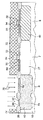
本発明の教示による、また注入されたベースを備えているNPNバイポーラ接合型トランジスタ構造用の選択的に蒸着されたエミッタを形成する工程の手順が、逐次的な処理工程によって形成された構造の横断面図を示した図1〜10を参照して下記に説明する。図示した従来技術の方法は、基板上にバイポーラトランジスタとCMOS(相補型金属酸化物電界効果トランジスタ)とが形成されるBiCMOS法である。この工程では、NPN BJTが領域6に形成され、NMOSFETが領域7に形成され、PMOSFETが基板10の領域8に形成される。図1を参照。
In accordance with the teachings of the present invention, a process sequence for forming a selectively deposited emitter for an NPN bipolar junction transistor structure having an implanted base is a cross-sectional structure formed by sequential processing steps. This will be described below with reference to FIGS. The illustrated prior art method is a BiCMOS method in which a bipolar transistor and a CMOS (complementary metal oxide field effect transistor) are formed on a substrate. In this step, NPN BJT is formed in
デバイス間の性能劣化と電気的なクロストークを避けるため、BJTとCMOSデバイスとを電気的に絶縁する必要がある。図示した実施例の方法はLOCOS(シリコンの局部的酸化)絶縁を採用している。LOCOS領域は先ずp形シリコン基板10(図1を参照)酸化させて、パッド酸化層とも呼ばれる二酸化シリコン層を形成することによって形成される。窒化シリコン層(図示せず)はシリコン二酸化層を覆って蒸着される。窒化シリコン層および二酸化シリコン層はこれを覆うパターン形成されたフォトレジスト層に従ってエッチングされ、その中に開口部が形成される。残りの領域は後のLOCOS酸化用の酸化マスクを形成し、基板10の酸化は窒化シリコンおよび二酸化シリコン層内の開口部を通してしか可能ではなくなる。LOCOS酸化工程は図1に示すように、絶縁性二酸化シリコン領域20を形成する。
In order to avoid performance degradation and electrical crosstalk between devices, it is necessary to electrically insulate the BJT from the CMOS device. The method of the illustrated embodiment employs LOCOS (local oxidation of silicon) insulation. The LOCOS region is formed by first oxidizing a p-type silicon substrate 10 (see FIG. 1) to form a silicon dioxide layer, also referred to as a pad oxide layer. A silicon nitride layer (not shown) is deposited over the silicon dioxide layer. The silicon nitride layer and the silicon dioxide layer are etched according to a patterned photoresist layer covering it, and an opening is formed therein. The remaining area forms an oxidation mask for subsequent LOCOS oxidation, and oxidation of the
絶縁領域20の形成後、窒化シリコンおよび二酸化シリコンの残りの領域は化学的に剥離され、隣接する絶縁領域20の間の領域の基板10上に犠牲二酸化シリコン層が形成される。
After the formation of the
別の実施形態では浅溝および深溝絶縁構造のような別の絶縁構造を単独で、または他の絶縁構造と組み合わせて用いることができる。 In other embodiments, other insulating structures, such as shallow and deep groove insulating structures, can be used alone or in combination with other insulating structures.
次に、フォトレジスト層が蒸着、マスキング、パターン形成、および形成されて、p−タブ・フォトレジスト注入マスク(図示せず)が形成される。p形ドーピング剤がマスクを通して注入され、基板10のNMOS領域7にp−タブ27が形成される。図1を参照。
Next, a photoresist layer is deposited, masked, patterned, and formed to form a p-tab photoresist implantation mask (not shown). A p-type dopant is implanted through the mask to form a p-
次に、n−タブ・フォトレジスト注入マスクが形成され、n形ドーピング剤がマスクを通して注入され、NPN BJTデバイス用のPMOS領域8とコレクタ領域42とが形成される。コレクタ領域42は(図2に関連して後述するように)、順次形成されるサブコレクタに接続されるためのシンカー領域としての役割を果たす。
Next, an n-tab photoresist implantation mask is formed and an n-type dopant is implanted through the mask to form
CMOSゲート・スタックを形成するため、ウエットクリーン工程によりn−タブ・フォトレジスト・マスクと犠牲二酸化シリコン層とを除去する。二酸化シリコン層、多結晶シリコン層、および珪化タングステン層は基板10の上面46上にブランケット蒸着される。
To form the CMOS gate stack, the n-tub photoresist mask and the sacrificial silicon dioxide layer are removed by a wet clean process. A silicon dioxide layer, a polycrystalline silicon layer, and a tungsten silicide layer are blanket deposited on the
多結晶シリコン層は注入マスクを通してドープされ、層がパターン形成されてゲート・スタック層が形成される。その結果生じるゲート・スタック構造は(NMOS領域7内の)p−タブ27および(PMOS領域8内の)n−タブ40のそれぞれの上方のゲート酸化物領域50と、多結晶シリコン領域52と、珪化タングステン領域54とを備えている。
The polycrystalline silicon layer is doped through an implantation mask and the layer is patterned to form a gate stack layer. The resulting gate stack structure includes a
適宜にパターン形成された注入マスクを利用して、p−タブ領域27にn形の軽くドープされたドレン領域61(NLDD)が形成され、BJT領域6にn形の軽くドープされたコレクタ接点領域62が形成される。適宜にパターン形成された注入マスクを利用して、n−タブ40にp形の軽くドープされたドレン領域67(PLDD)が形成される。
Using an appropriately patterned implantation mask, an n-type lightly doped drain region 61 (NLDD) is formed in the p-
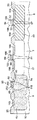
TEOS(テトラエトキシシラン)二酸化シリコン層68が基板10を覆って形成される。図2を参照。サブコレクタ・マスク72を使用して、サブコレクタ74が(n形注入矢印76で示されているように)BJT領域6に注入される。サブコレクタ74の形成後、p形ベース75がp形ドーピング剤を使用した注入カウンタードーピングによってサブコレクタ74を覆って形成される。
A TEOS (tetraethoxysilane)
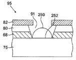
図3に示すように、スペーサ二酸化シリコン層80が基板10上に蒸着される。一実施形態では、層80はTEOS工程によって形成される。一実施形態では、後続のウエットエッチング工程でマスクとして機能するように、比較的薄い非晶質シリコン層82が二酸化シリコン層80上に形成される。パターン形成されたフォトレジスト層(図示せず)を利用して、非晶質シリコン層82と、その下層の二酸化シリコン層80とが異方性エッチングされてエミッタ・ウインドウ91が形成される。エッチング工程はTEOS層68上で停止され、図示のとおり、この層は後続のウエットエッチング工程中にエミッタ・ウインドウ91から除去される。
A spacer
先行技術では、多結晶シリコン(図示せず)はBJTエミッタを形成する際に使用されるためにブランケット蒸着される(エミッタ・ウインドウ91内も含む)。多結晶シリコン層には砒素または別のn形ドーピング剤が注入(または現場ドーピング)される。 In the prior art, polycrystalline silicon (not shown) is blanket deposited (including within emitter window 91) for use in forming BJT emitters. The polycrystalline silicon layer is implanted (or in-situ doped) with arsenic or another n-type dopant.
蒸着およびパターン形成の代わりに、本発明の教示によれば、シリコン・エミッタ250(図4を参照)がベース75の表面252(シリコン)上のエミッタ・ウインドウ91内に選択的に蒸着される。図5の拡大図をも参照されたい。選択的な蒸着とは、二酸化シリコンまたは窒化シリコン上にではなく、純正なシリコン上にシリコンを蒸着することを意味している。選択的なシリコン蒸着は、ベース75のシリコン面252のような純正なシリコンが露出している領域だけでシリコンの蒸着が可能であるように、(一実施形態では)塩化水素酸(HCI)環境で行われる。実際には、シリコンは基板10の全体に成長するが、誘電面上でのシリコン・エッチング速度はこれらの誘電面上での成長速度よりも速い。したがって、シリコンはシリコン面上でのみ選択的に蒸着される。
Instead of deposition and patterning, in accordance with the teachings of the present invention, a silicon emitter 250 (see FIG. 4) is selectively deposited in an
本発明の教示によって形成されたエミッタは現場ドーピングされ、または蒸着後に注入される。ドーピング剤を注入するには、一実施形態では基板10のエミッタ250以外の領域でのドーピング剤の注入を防ぐためにマスクが形成される。別の実施形態では、注入工程用の適当なマスクを形成することがある、基板10を覆う二酸化シリコン層82の厚さによっては、マスクが不要であることもある。
Emitters formed in accordance with the teachings of the present invention are in-situ doped or implanted after deposition. To implant the dopant, in one embodiment, a mask is formed to prevent implantation of the dopant in regions other than the
有利なことには、エミッタ250の蒸着およびパターン形成は同じ工程で行われる。したがって、エミッタを形成するためにブランケット多結晶シリコンのエッチングに関連する従来の工程は必要ない。
Advantageously, the deposition and patterning of the
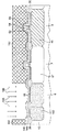
PMOSFETおよびNMOSFETデバイス用のゲート・スタック・スペーサ100は層82を除去し、二酸化シリコン層80を異方性エッチングすることによって形成される。このエッチング工程中、TEOS二酸化シリコン層68も除去される。図6に示された形成された構造を参照されたい。
フォトレジスト層は、大量の(n+)砒素をp−タブ27に注入し、NMOS領域6用のソース106およびドレン108を形成するためのn+ソース/ドレン・マスクを形成するために蒸着され、パターン形成される。図7を参照。砒素は同じマスクを通してBJTコレクタ領域42にも注入され、引き続き形成される被覆コレクタ接点との接触抵抗を最小限にするため、ドーピング・レベルが比較的高いn+オーム・コレクタ接点領域110を形成する。
A photoresist layer is deposited to form a n + source / drain mask to implant a large amount of (n +) arsenic into the p-
大量のp形ドーピング剤がパターン形成されたマスクを通してn−タブ40へと注入されて、PMOS領域8用のソース114とドレン116とが形成される。NPN BJT95の外部ベース領域118もp形ドーピング剤によって形成される。このように、図10は基板を覆う誘電層、および基板10内に形成されたドーピング領域を相互接続するための金属化層の間に配置された付加的な誘電層の蒸着前の最終的なデバイスの外見を示している。
A large amount of p-type dopant is implanted into the n-
選択的に蒸着されるエミッタを形成するための本発明の教示内容を、多結晶シリコン層から形成されたベース領域を備えたNPN BJTを形成するために応用する態様が図8−14に示されており、これらの図面は逐次的な工程により形成された構造の横断面図を示している。図示した方法は、バイポーラトランジスタおよびCMOS(相補型金属酸化物半導体電界効果トランジスタ)が基板上に形成されるBiCMOS方法である。本発明の教示内容は、同じ基板上にCMOSトランジスタが形成されずに、基板上にBJTが形成される場合にも応用できる。 An embodiment of applying the teachings of the present invention for forming selectively deposited emitters to form an NPN BJT with a base region formed from a polycrystalline silicon layer is shown in FIGS. 8-14. These drawings show cross-sectional views of structures formed by sequential processes. The illustrated method is a BiCMOS method in which bipolar transistors and CMOS (complementary metal oxide semiconductor field effect transistors) are formed on a substrate. The teachings of the present invention can also be applied to the case where BJTs are formed on a substrate without forming CMOS transistors on the same substrate.
多結晶シリコン・ベースを備えた実施形態の初期の工程は、注入されたベース領域に関して上記で図1に開示した工程と実質的に同じである。図1に示した工程に続く、多結晶シリコン・ベースの追加の工程は図8から始まって示されている。 The initial steps of the embodiment with a polycrystalline silicon base are substantially the same as those disclosed above in FIG. 1 with respect to the implanted base region. An additional step of polycrystalline silicon base following the step shown in FIG. 1 is shown beginning with FIG.
図8は適宜にパターン形成されたマスク(図示せず)を通したn形注入ドーピングによって形成されたサブコレクタ142を示している。TEOSスペーサ酸化物層144および多結晶シリコン層146が基板10上に形成されている。多結晶シリコン層146は注入マスク150を通して大量のホウ素注入(注入矢印148で示されている)でドーピングされる。ホウ素が注入された多結晶シリコン層146は後述のように外部ベース領域を形成する。
FIG. 8 shows a
図9に示すように、窒化シリコン層156および二酸化シリコン層158(一実施形態ではTEOS工程によって形成される)多結晶シリコン層146を覆って蒸着される。フォトレジスト層160が蒸着され、パターン形成されて、内部にウインドウ162が形成される。二酸化シリコン層158、窒化シリコン層156、および多結晶シリコン層146はウインドウ162を通して異方性エッチングされ、TEOS層144で停止されて、基板10内にエミッタ・ウインドウ163が形成される。ある実施形態では、コレクタ領域166がウインドウ162を経て注入される。
As shown in FIG. 9, a
二酸化シリコン層158とフォトレジスト層160が除去された後、窒化シリコン層が蒸着され、異方性エッチングされて、側壁スペーサ170が形成される。図10を参照。ウエットエッチングがエミッタ・ウインドウ163の内部から二酸化シリコンTEOS層68および144を除去して、一次空隙174と、一次空隙174に対して横に配置された空隙175とを形成する。
After the
双方とも参照符号176で示されている(図11を参照)真性ベースおよびキャップ領域はシリコン−ゲルマニウムのエピタキシャル成長工程中に空隙174および175内に形成される。
The intrinsic base and cap regions, both indicated by reference numeral 176 (see FIG. 11), are formed in the
窒化シリコン・スペーサ180およびその下層の二酸化シリコン(TEOS)スペーサ182は図12の拡大図に示すようにウインドウ163内に形成される。後に形成されるn+エミッタとp+外部ベースとの間のスペースを拡大する役割を果たすスペーサはTEOS二酸化シリコン層と窒化シリコン層とを蒸着することによって形成される。これらの層は再び異方性エッチングされて、スペーサ180および182が形成され、その際にエッチングは真性ベースおよびキャップ領域176の上面に形成されたTEOS層の領域で停止される。別の実施形態では、以前形成されたスペーサ170で充分であるので、スペーサ180および182は必要ない。スペーサの形成に引き続いて、真性ベースおよびキャップ領域176の上面を覆うTEOS二酸化シリコン層の残りの部分はウエットエッチング工程によって除去される。
図12にさらに示すように、エミッタ260は前述のように(一実施形態では)塩化水素酸(HCI)環境で、真性ベース176のシリコン面262上だけにしかシリコンが蒸着できないように選択的に蒸着される。エミッタは現場ドーピングがされることも、蒸着後に注入されることもできる。注入工程は、ベースの多結晶シリコン層146を覆う窒化シリコン層156の厚みに応じてマスクを使用して実施しても、使用しないで実施してもよい。すなわち、窒化シリコン層156がエミッタ260内を除く全ての領域で注入されたドーピング剤を遮断するのに充分に厚い場合は、マスク層は必要ないであろう。
As further shown in FIG. 12,
BiCMOS方法は多結晶シリコン層146をエッチングするためにパターン形成されたハード・マスクまたはフォトレジスト・マスクを使用して継続され、外部ベース領域146Aが形成される。この時点で、BJTの方法は基本的に完了である。(図13に示すように)BJTは、真性ベース176、(ドーピングされた多結晶シリコンから形成された)外部ベース領域146A、選択的に蒸着されたエミッタ260、およびコレクタ領域42、142および66を備えている。
The BiCMOS method is continued using a patterned hard mask or photoresist mask to etch the
図13にさらに示すように、スペーサ・エッチング工程はTEOS層144および窒化シリコン層156を異方性エッチングしてゲート・スタック用のスペーサ202を形成する。
n形不純物が適宜にパターン形成されたマスクを通して注入され、ソース/ドレン領域214およびコレクタ領域213が形成される。図14を参照。P形不純物はn−タブ40に注入されてソース/ドレン領域218が形成される。
As further shown in FIG. 13, the spacer etch step anisotropically etches the
N-type impurities are implanted through an appropriately patterned mask to form source /
図14は第1誘電層および第1相互接続金属化層の蒸着前の様々な素子の好適な最終構造を示している。当分野で公知のように、第1誘電層にウインドウが画成され、BJTおよび2つのMOSFETの様々な領域との電気的接触を確立するために、第1誘電層内に導電性プラグが形成される。領域を接続するための相互接続構造は第1金属化層内に形成される。第1金属化層の上方に付加的な交互の誘電層と相互接続層とが形成されて、集積回路の相互接続システムが完成される。 FIG. 14 shows the preferred final structure of the various devices prior to the deposition of the first dielectric layer and the first interconnect metallization layer. As is known in the art, a window is defined in the first dielectric layer and conductive plugs are formed in the first dielectric layer to establish electrical contact with the various regions of the BJT and the two MOSFETs. Is done. An interconnect structure for connecting the regions is formed in the first metallization layer. Additional alternating dielectric and interconnect layers are formed above the first metallization layer to complete the integrated circuit interconnect system.
(注入をベースにした実施形態でも、多結晶シリコンをベースにした実施形態でも)本発明の教示内容によって形成されたエミッタは単結晶または多結晶材料から形成されることをこれまで見てきた。金属の結晶構造は成長の条件、成長面の清浄技術、およびその他の工程パラメータによって左右される。単結晶と多結晶のエミッタの双方の実施形態とも受け入れられる。 It has been seen so far that emitters formed according to the teachings of the present invention (both implant-based and polycrystalline silicon-based embodiments) are formed from single crystal or polycrystalline materials. The crystal structure of the metal depends on growth conditions, growth surface cleaning techniques, and other process parameters. Both single crystal and polycrystalline emitter embodiments are acceptable.
本発明によって、エミッタ領域はベース・シリコンの上方でしか蒸着されないので、エミッタが蒸着された多結晶シリコン層から形成された場合に発生する不都合なウインドウ狭窄効果なしで、エミッタ・ウインドウの幅を従来技術と比較して大幅に縮小できる。このように、本発明によって形成されたBJTはより狭いエミッタ・ウインドウを使用することによってさらに高い動作速度をもたらす。さらに、エミッタ多結晶シリコン層がないので、BJT構造の全長は先行技術のBJTと比較して短縮される。外部ベース領域146Aとエミッタとの間に窒化シリコン領域156A(図13を参照)を形成するためにエッチングされる厚い窒化シリコン絶縁層156は、ベース/エミッタのキャパシタンスを低減するため必要ない。さらに、導電性の相互接続が上に形成される最低部の誘電層の厚さも縮小される。
By virtue of the present invention, the emitter region is deposited only above the base silicon, so that the width of the emitter window is conventionally reduced without the inconvenient window constriction effect that occurs when the emitter is formed from a deposited polysilicon layer. It can be greatly reduced compared to technology. Thus, the BJT formed according to the present invention provides a higher operating speed by using a narrower emitter window. Furthermore, since there is no emitter polycrystalline silicon layer, the overall length of the BJT structure is reduced compared to the prior art BJT. A thick silicon
エミッタを選択的に蒸着することによって本発明は、先行技術のエミッタ・ウインドウ91を横切るエミッタ多結晶シリコン層の厚さの変化によって、エミッタ−ベース・インターフェースで砒素のn形ドーピング剤の濃度が変化するいわゆる「プラグ作用」を改善する。本発明の教示による選択的に蒸着されたエミッタ(250または260)のプロファイルは厚さの大幅な変動を生じないので、「プラグ作用」が回避される。
By selectively depositing the emitter, the present invention changes the concentration of the arsenic n-type dopant at the emitter-base interface by changing the thickness of the emitter polysilicon layer across the prior
さらに先行技術の方法では、エミッタは開口部の底面と側面上で成長し、開口部の側面よりも底面上の方が厚いエミッタになることがある。ある状況では、側面上に形成される材料は収斂し、蒸着工程を「ピンチオフ」し、ピンチオフ領域と開口部のベースとの間に空隙が生ずる。このように不適切に形成されたエミッタは、ベース領域に接触する充分なエミッタ材料が不足しているのでBJTの動作を損なうことがある。本発明の教示によってエミッタは選択的蒸着工程中に底部から開口部を埋めてゆくので、この欠点は回避される。 Further, in prior art methods, the emitters may grow on the bottom and side surfaces of the opening, and may be thicker on the bottom surface than the side surfaces of the opening. In some situations, the material formed on the sides converges and “pinch off” the deposition process, creating a gap between the pinch off region and the base of the opening. Such improperly formed emitters can impair the operation of the BJT due to lack of sufficient emitter material to contact the base region. This disadvantage is avoided because the teachings of the present invention fill the opening from the bottom during the selective deposition process.
半導体基板内にBJTのエミッタ層を形成するために有用な構造および方法をこれまで記載してきた。本発明の特定の用途と実施例を図示し、説明してきたが、これらは本発明を多様な態様と多様な回路構造で実施する基礎となるものである。本発明の範囲内で多くの変化形が可能である。記載した1つまたは複数の実施形態に関連する特徴および要素は全ての実施形態に必要な要素であると見なされるものではない。本発明は特許請求の範囲によってのみ限定されるものである。 A structure and method useful for forming a BJT emitter layer in a semiconductor substrate has been described. While specific uses and embodiments of the invention have been illustrated and described, they serve as the basis for implementing the invention in various embodiments and circuit structures. Many variations are possible within the scope of the present invention. The features and elements associated with one or more of the described embodiments are not to be considered as necessary elements for all embodiments. The present invention is limited only by the claims.
Claims (33)
内部にベースを有する基板を準備する工程と、
前記基板を覆う材料層を形成する工程と、
前記ベースを露出させる開口部を前記材料層に形成する工程と、
前記エミッタを前記開口部内に選択的に蒸着する工程と
を含む方法。 A method of forming an emitter of a bipolar junction transistor comprising:
Preparing a substrate having a base therein;
Forming a material layer covering the substrate;
Forming an opening in the material layer to expose the base;
Selectively depositing the emitter into the opening.
基板を準備する工程と、
前記基板内にコレクタを形成する工程と、
前記基板内に真性ベースを形成し、前記コレクタを覆う工程と、
前記真性ベースを覆う1つまたは複数の材料層を形成する工程と、
前記1つまたは複数の材料層内に、前記真性ベースの方向に下方に延びる開口部を形成する工程と、
前記開口部内の前記真性ベースから上方にエミッタを選択的に蒸着する工程と、
前記真性ベースの少なくとも一部を覆う外部ベースを形成する工程と
を含む方法。 A method of forming an emitter of a bipolar junction transistor comprising:
Preparing a substrate;
Forming a collector in the substrate;
Forming an intrinsic base in the substrate and covering the collector;
Forming one or more material layers covering the intrinsic base;
Forming an opening in the one or more material layers extending downward in the direction of the intrinsic base;
Selectively depositing an emitter upward from the intrinsic base in the opening;
Forming an external base covering at least a portion of the intrinsic base.
基板を準備する工程と、
前記基板内にコレクタを形成する工程と、
前記基板内に前記コレクタを覆う真性ベースを形成する工程と、
前記真性ベースを覆う材料層を形成する工程と、
前記材料層内に、側壁を備え、前記真性ベースの方向に下方に延びる開口部を形成する工程と、
前記側壁に沿って誘電巣スペーサを形成する工程と、
前記開口部内の前記真性ベースから上方にエミッタを選択的に蒸着する工程と
を含む方法。 A method of forming an emitter of a bipolar junction transistor comprising:
Preparing a substrate;
Forming a collector in the substrate;
Forming an intrinsic base covering the collector in the substrate;
Forming a material layer covering the intrinsic base;
Forming an opening in the material layer comprising a side wall and extending downward in the direction of the intrinsic base;
Forming a dielectric nest spacer along the sidewall;
Selectively depositing an emitter above the intrinsic base in the opening.
基板と、
前記基板内に配置されたコレクタと、
前記コレクタを覆う真性ベースと、
前記真性ベースと接触する外部ベースと、
前記真性ベースおよび前記外部ベースを覆い、開口部が画成されている誘電層と、
前記開口部内にあり、前記開口部内に局限されたエミッタと
を備えるバイポーラ接合型トランジスタ。 A bipolar junction transistor,
A substrate,
A collector disposed within the substrate;
An intrinsic base covering the collector;
An external base in contact with the intrinsic base;
A dielectric layer covering the intrinsic base and the external base and having an opening defined;
A bipolar junction transistor having an emitter in the opening and localized in the opening.
半導体基板と、
前記基板内に形成されたコレクタ領域と、
基板内に形成された、前記コレクタ領域を覆うベース領域と、
前記基板を覆い、内部にウインドウが形成された材料層と、
前記ウインドウ内だけに形成されたエミッタ領域と
を備えるバイポーラ接合型トランジスタ。 A bipolar junction transistor,
A semiconductor substrate;
A collector region formed in the substrate;
A base region formed in the substrate and covering the collector region;
A material layer covering the substrate and having a window formed therein;
A bipolar junction transistor comprising an emitter region formed only within the window.
29. The bipolar junction transistor of claim 28, wherein the emitter exhibits a substantially constant dopant concentration.
Applications Claiming Priority (1)
| Application Number | Priority Date | Filing Date | Title |
|---|---|---|---|
| US50737403P | 2003-09-30 | 2003-09-30 |
Publications (1)
| Publication Number | Publication Date |
|---|---|
| JP2005109501A true JP2005109501A (en) | 2005-04-21 |
Family
ID=34312474
Family Applications (1)
| Application Number | Title | Priority Date | Filing Date |
|---|---|---|---|
| JP2004283339A Pending JP2005109501A (en) | 2003-09-30 | 2004-09-29 | Bipolar transistor with selectively deposited emitter |
Country Status (5)
| Country | Link |
|---|---|
| US (1) | US20050098852A1 (en) |
| EP (1) | EP1521306A2 (en) |
| JP (1) | JP2005109501A (en) |
| KR (1) | KR20050032014A (en) |
| TW (1) | TW200518341A (en) |
Families Citing this family (5)
| Publication number | Priority date | Publication date | Assignee | Title |
|---|---|---|---|---|
| KR100731087B1 (en) * | 2005-10-28 | 2007-06-22 | 동부일렉트로닉스 주식회사 | BiCMOS device for using power and method for manufacturing the same |
| US20070278539A1 (en) * | 2006-06-02 | 2007-12-06 | Agere Systems Inc. | Junction field effect transistor and method for manufacture |
| US7572708B1 (en) | 2007-03-08 | 2009-08-11 | National Semiconductor Corporation | Utilization of doped glass on the sidewall of the emitter window in a bipolar transistor structure |
| CN111554734A (en) | 2018-06-28 | 2020-08-18 | 联华电子股份有限公司 | Semiconductor structure and manufacturing method thereof |
| US11094599B2 (en) | 2018-06-28 | 2021-08-17 | United Microelectronics Corp. | Semiconductor structure and manufacturing method thereof |
Family Cites Families (24)
| Publication number | Priority date | Publication date | Assignee | Title |
|---|---|---|---|---|
| JPS63107167A (en) * | 1986-10-24 | 1988-05-12 | Oki Electric Ind Co Ltd | Manufacture of semiconductor integrated circuit device |
| US5059544A (en) * | 1988-07-14 | 1991-10-22 | International Business Machines Corp. | Method of forming bipolar transistor having self-aligned emitter-base using selective and non-selective epitaxy |
| JPH02280340A (en) * | 1989-04-21 | 1990-11-16 | Hitachi Ltd | Manufacture of semiconductor integrated circuit device |
| US4988632A (en) * | 1990-01-02 | 1991-01-29 | Motorola, Inc. | Bipolar process using selective silicon deposition |
| US5064774A (en) * | 1991-02-19 | 1991-11-12 | Motorola, Inc. | Self-aligned bipolar transistor process |
| JP3132101B2 (en) * | 1991-11-20 | 2001-02-05 | 日本電気株式会社 | Method for manufacturing semiconductor device |
| US5321301A (en) * | 1992-04-08 | 1994-06-14 | Nec Corporation | Semiconductor device |
| JPH05347311A (en) * | 1992-06-15 | 1993-12-27 | Nec Corp | Manufacture of semiconductor device |
| JP2503878B2 (en) * | 1993-06-14 | 1996-06-05 | 日本電気株式会社 | Semiconductor integrated circuit device and manufacturing method thereof |
| JP2531355B2 (en) * | 1993-06-30 | 1996-09-04 | 日本電気株式会社 | Bipolar transistor and manufacturing method thereof |
| JP2746225B2 (en) * | 1995-10-16 | 1998-05-06 | 日本電気株式会社 | Semiconductor device and manufacturing method thereof |
| SE508635C2 (en) * | 1995-11-20 | 1998-10-26 | Ericsson Telefon Ab L M | Method for selective etching in the manufacture of a bipolar transistor with self-registering base-emitter structure |
| US5773350A (en) * | 1997-01-28 | 1998-06-30 | National Semiconductor Corporation | Method for forming a self-aligned bipolar junction transistor with silicide extrinsic base contacts and selective epitaxial grown intrinsic base |
| US6248650B1 (en) * | 1997-12-23 | 2001-06-19 | Texas Instruments Incorporated | Self-aligned BJT emitter contact |
| US6020246A (en) * | 1998-03-13 | 2000-02-01 | National Semiconductor Corporation | Forming a self-aligned epitaxial base bipolar transistor |
| US6359317B1 (en) * | 1998-12-28 | 2002-03-19 | Agere Systems Guardian Corp. | Vertical PNP bipolar transistor and its method of fabrication |
| FR2799048B1 (en) * | 1999-09-23 | 2003-02-21 | St Microelectronics Sa | METHOD FOR MANUFACTURING A SELF-ALIGNED VERTICAL BIPOLAR TRANSISTOR |
| FR2805923B1 (en) * | 2000-03-06 | 2002-05-24 | St Microelectronics Sa | PROCESS FOR MANUFACTURING A SELF-ALIGNED DOUBLE-POLYSILICON BIPOLAR TRANSISTOR |
| FR2806831B1 (en) * | 2000-03-27 | 2003-09-19 | St Microelectronics Sa | METHOD FOR MANUFACTURING A BIPOLAR SELF-ALIGNED DOUBLE-POLYSILICIUM TYPE BIPOLAR TRANSISTOR AND CORRESPONDING TRANSISTOR |
| TW472394B (en) * | 2000-05-03 | 2002-01-11 | Ind Tech Res Inst | A bipolar transistor process with epitaxial base |
| US6495904B1 (en) * | 2000-08-23 | 2002-12-17 | National Semiconductor Corporation | Compact bipolar transistor structure |
| US6492237B2 (en) * | 2001-02-12 | 2002-12-10 | Maxim Integrated Products, Inc. | Method of forming an NPN device |
| US6617619B1 (en) * | 2002-02-04 | 2003-09-09 | Newport Fab, Llc | Structure for a selective epitaxial HBT emitter |
| US6586307B1 (en) * | 2002-02-14 | 2003-07-01 | Newport Fab, Llc | Method for controlling an emitter window opening in an HBT and related structure |
-
2004
- 2004-09-29 JP JP2004283339A patent/JP2005109501A/en active Pending
- 2004-09-29 TW TW093129462A patent/TW200518341A/en unknown
- 2004-09-29 US US10/953,476 patent/US20050098852A1/en not_active Abandoned
- 2004-09-29 EP EP04255999A patent/EP1521306A2/en active Pending
- 2004-09-30 KR KR1020040078077A patent/KR20050032014A/en not_active Application Discontinuation
Also Published As
| Publication number | Publication date |
|---|---|
| KR20050032014A (en) | 2005-04-06 |
| EP1521306A2 (en) | 2005-04-06 |
| TW200518341A (en) | 2005-06-01 |
| US20050098852A1 (en) | 2005-05-12 |
Similar Documents
| Publication | Publication Date | Title |
|---|---|---|
| US8129234B2 (en) | Method of forming bipolar transistor integrated with metal gate CMOS devices | |
| US8476675B2 (en) | Semiconductor device and method of manufacture thereof | |
| JPH0677421A (en) | Manufacture of transistor | |
| EP1512172B1 (en) | Method of fabrication sige heterojunction bipolar transistor | |
| JP2009141375A (en) | Semiconductor process and integrated circuit | |
| JPH0744232B2 (en) | Bi-CMOS device manufacturing method | |
| US8084313B2 (en) | Method for forming a bipolar junction transistor and a metal oxide semiconductor field effect transistor | |
| JP2004241779A (en) | METHOD FOR MANUFACTURING BiCMOS USING SELF ALIGNMENT | |
| US20070161173A1 (en) | Process to integrate fabrication of bipolar devices into a CMOS process flow | |
| US7863148B2 (en) | Method for integrating SiGe NPN and vertical PNP devices | |
| JPH05198752A (en) | Mos device and manufacture of semiconductor structure with bipolar-device | |
| WO2001075968A2 (en) | Method of manufacturing a heterojunction bicmos integrated circuit | |
| JP2005109501A (en) | Bipolar transistor with selectively deposited emitter | |
| JP2006210914A (en) | Bipolar transistor and forming method thereof | |
| JP4988339B2 (en) | Bipolar transistor having high fT and fmax and method of manufacturing the same | |
| JP2003068754A (en) | Semiconductor structure including bipolar transistor | |
| US6790736B2 (en) | Method for manufacturing and structure of semiconductor device with polysilicon definition structure | |
| EP2506297A1 (en) | Bi-CMOS Device and Method | |
| JPH08293604A (en) | Transistor with metal gate electrode and its preparation | |
| JP3062028B2 (en) | Method for manufacturing semiconductor device | |
| JP2836393B2 (en) | Semiconductor device and manufacturing method thereof | |
| JPH08162632A (en) | Semiconductor device and manufacture thereof | |
| JPH08148590A (en) | Semiconductor device and its manufacture | |
| JPH08288466A (en) | Mos semiconductor device and its manufacture | |
| JP2004103838A (en) | Method for manufacturing semiconductor device |