JP2005100977A - Electroluminescent element and light-emitting device using the same - Google Patents
Electroluminescent element and light-emitting device using the same Download PDFInfo
- Publication number
- JP2005100977A JP2005100977A JP2004246119A JP2004246119A JP2005100977A JP 2005100977 A JP2005100977 A JP 2005100977A JP 2004246119 A JP2004246119 A JP 2004246119A JP 2004246119 A JP2004246119 A JP 2004246119A JP 2005100977 A JP2005100977 A JP 2005100977A
- Authority
- JP
- Japan
- Prior art keywords
- electron
- electroluminescent
- layer
- light
- electron transport
- Prior art date
- Legal status (The legal status is an assumption and is not a legal conclusion. Google has not performed a legal analysis and makes no representation as to the accuracy of the status listed.)
- Withdrawn
Links
- 239000000463 material Substances 0.000 claims abstract description 256
- 150000002894 organic compounds Chemical class 0.000 claims abstract description 15
- 125000006575 electron-withdrawing group Chemical group 0.000 claims description 41
- 230000005524 hole trap Effects 0.000 claims description 29
- 238000000295 emission spectrum Methods 0.000 claims description 22
- MPKKHQRPBMSEND-UHFFFAOYSA-N 2-pyran-4-ylidenepropanedinitrile Chemical group N#CC(C#N)=C1C=COC=C1 MPKKHQRPBMSEND-UHFFFAOYSA-N 0.000 claims description 6
- 125000005843 halogen group Chemical group 0.000 claims description 6
- 150000004982 aromatic amines Chemical group 0.000 claims description 5
- 125000002915 carbonyl group Chemical group [*:2]C([*:1])=O 0.000 claims description 5
- 125000004093 cyano group Chemical group *C#N 0.000 claims description 5
- 150000004945 aromatic hydrocarbons Chemical class 0.000 claims description 3
- 229910021387 carbon allotrope Inorganic materials 0.000 claims description 3
- 125000004432 carbon atom Chemical group C* 0.000 claims description 3
- 238000005401 electroluminescence Methods 0.000 claims description 3
- 230000005525 hole transport Effects 0.000 abstract description 29
- 230000032258 transport Effects 0.000 description 62
- 239000010408 film Substances 0.000 description 43
- 239000000758 substrate Substances 0.000 description 36
- 238000000034 method Methods 0.000 description 28
- 238000002347 injection Methods 0.000 description 26
- 239000007924 injection Substances 0.000 description 26
- 238000001771 vacuum deposition Methods 0.000 description 23
- 230000000052 comparative effect Effects 0.000 description 20
- IBHBKWKFFTZAHE-UHFFFAOYSA-N n-[4-[4-(n-naphthalen-1-ylanilino)phenyl]phenyl]-n-phenylnaphthalen-1-amine Chemical group C1=CC=CC=C1N(C=1C2=CC=CC=C2C=CC=1)C1=CC=C(C=2C=CC(=CC=2)N(C=2C=CC=CC=2)C=2C3=CC=CC=C3C=CC=2)C=C1 IBHBKWKFFTZAHE-UHFFFAOYSA-N 0.000 description 16
- 229910052782 aluminium Inorganic materials 0.000 description 13
- VSSSHNJONFTXHS-UHFFFAOYSA-N coumarin 153 Chemical compound C12=C3CCCN2CCCC1=CC1=C3OC(=O)C=C1C(F)(F)F VSSSHNJONFTXHS-UHFFFAOYSA-N 0.000 description 12
- -1 N-carbazolyl Chemical group 0.000 description 11
- 238000010438 heat treatment Methods 0.000 description 10
- XAGFODPZIPBFFR-UHFFFAOYSA-N aluminium Chemical compound [Al] XAGFODPZIPBFFR-UHFFFAOYSA-N 0.000 description 9
- 238000010549 co-Evaporation Methods 0.000 description 9
- 229910052751 metal Inorganic materials 0.000 description 9
- 239000002184 metal Substances 0.000 description 9
- 239000011701 zinc Substances 0.000 description 9
- 229910004261 CaF 2 Inorganic materials 0.000 description 8
- UFVXQDWNSAGPHN-UHFFFAOYSA-K bis[(2-methylquinolin-8-yl)oxy]-(4-phenylphenoxy)alumane Chemical compound [Al+3].C1=CC=C([O-])C2=NC(C)=CC=C21.C1=CC=C([O-])C2=NC(C)=CC=C21.C1=CC([O-])=CC=C1C1=CC=CC=C1 UFVXQDWNSAGPHN-UHFFFAOYSA-K 0.000 description 8
- 238000010586 diagram Methods 0.000 description 8
- 239000011521 glass Substances 0.000 description 8
- 150000001875 compounds Chemical class 0.000 description 7
- JBPCDMSEJVCNGV-UHFFFAOYSA-N coumarin 334 Chemical compound C1CCC2=C(OC(C(C(=O)C)=C3)=O)C3=CC3=C2N1CCC3 JBPCDMSEJVCNGV-UHFFFAOYSA-N 0.000 description 7
- 239000012212 insulator Substances 0.000 description 7
- 238000005215 recombination Methods 0.000 description 7
- 230000006798 recombination Effects 0.000 description 7
- SPDPTFAJSFKAMT-UHFFFAOYSA-N 1-n-[4-[4-(n-[4-(3-methyl-n-(3-methylphenyl)anilino)phenyl]anilino)phenyl]phenyl]-4-n,4-n-bis(3-methylphenyl)-1-n-phenylbenzene-1,4-diamine Chemical group CC1=CC=CC(N(C=2C=CC(=CC=2)N(C=2C=CC=CC=2)C=2C=CC(=CC=2)C=2C=CC(=CC=2)N(C=2C=CC=CC=2)C=2C=CC(=CC=2)N(C=2C=C(C)C=CC=2)C=2C=C(C)C=CC=2)C=2C=C(C)C=CC=2)=C1 SPDPTFAJSFKAMT-UHFFFAOYSA-N 0.000 description 5
- CRHRWHRNQKPUPO-UHFFFAOYSA-N 4-n-naphthalen-1-yl-1-n,1-n-bis[4-(n-naphthalen-1-ylanilino)phenyl]-4-n-phenylbenzene-1,4-diamine Chemical compound C1=CC=CC=C1N(C=1C2=CC=CC=C2C=CC=1)C1=CC=C(N(C=2C=CC(=CC=2)N(C=2C=CC=CC=2)C=2C3=CC=CC=C3C=CC=2)C=2C=CC(=CC=2)N(C=2C=CC=CC=2)C=2C3=CC=CC=C3C=CC=2)C=C1 CRHRWHRNQKPUPO-UHFFFAOYSA-N 0.000 description 5
- 239000007983 Tris buffer Substances 0.000 description 5
- 229910045601 alloy Inorganic materials 0.000 description 5
- 239000000956 alloy Substances 0.000 description 5
- 229910052744 lithium Inorganic materials 0.000 description 5
- 238000004519 manufacturing process Methods 0.000 description 5
- 238000004544 sputter deposition Methods 0.000 description 5
- IYZMXHQDXZKNCY-UHFFFAOYSA-N 1-n,1-n-diphenyl-4-n,4-n-bis[4-(n-phenylanilino)phenyl]benzene-1,4-diamine Chemical compound C1=CC=CC=C1N(C=1C=CC(=CC=1)N(C=1C=CC(=CC=1)N(C=1C=CC=CC=1)C=1C=CC=CC=1)C=1C=CC(=CC=1)N(C=1C=CC=CC=1)C=1C=CC=CC=1)C1=CC=CC=C1 IYZMXHQDXZKNCY-UHFFFAOYSA-N 0.000 description 4
- ZVFQEOPUXVPSLB-UHFFFAOYSA-N 3-(4-tert-butylphenyl)-4-phenyl-5-(4-phenylphenyl)-1,2,4-triazole Chemical compound C1=CC(C(C)(C)C)=CC=C1C(N1C=2C=CC=CC=2)=NN=C1C1=CC=C(C=2C=CC=CC=2)C=C1 ZVFQEOPUXVPSLB-UHFFFAOYSA-N 0.000 description 4
- DHDHJYNTEFLIHY-UHFFFAOYSA-N 4,7-diphenyl-1,10-phenanthroline Chemical compound C1=CC=CC=C1C1=CC=NC2=C1C=CC1=C(C=3C=CC=CC=3)C=CN=C21 DHDHJYNTEFLIHY-UHFFFAOYSA-N 0.000 description 4
- NRTOMJZYCJJWKI-UHFFFAOYSA-N Titanium nitride Chemical compound [Ti]#N NRTOMJZYCJJWKI-UHFFFAOYSA-N 0.000 description 4
- 239000000969 carrier Substances 0.000 description 4
- VPUGDVKSAQVFFS-UHFFFAOYSA-N coronene Chemical compound C1=C(C2=C34)C=CC3=CC=C(C=C3)C4=C4C3=CC=C(C=C3)C4=C2C3=C1 VPUGDVKSAQVFFS-UHFFFAOYSA-N 0.000 description 4
- 238000001704 evaporation Methods 0.000 description 4
- 230000005284 excitation Effects 0.000 description 4
- 230000005281 excited state Effects 0.000 description 4
- 238000004768 lowest unoccupied molecular orbital Methods 0.000 description 4
- BASFCYQUMIYNBI-UHFFFAOYSA-N platinum Chemical compound [Pt] BASFCYQUMIYNBI-UHFFFAOYSA-N 0.000 description 4
- 239000000565 sealant Substances 0.000 description 4
- 238000007789 sealing Methods 0.000 description 4
- 239000010409 thin film Substances 0.000 description 4
- 238000007738 vacuum evaporation Methods 0.000 description 4
- FQJQNLKWTRGIEB-UHFFFAOYSA-N 2-(4-tert-butylphenyl)-5-[3-[5-(4-tert-butylphenyl)-1,3,4-oxadiazol-2-yl]phenyl]-1,3,4-oxadiazole Chemical compound C1=CC(C(C)(C)C)=CC=C1C1=NN=C(C=2C=C(C=CC=2)C=2OC(=NN=2)C=2C=CC(=CC=2)C(C)(C)C)O1 FQJQNLKWTRGIEB-UHFFFAOYSA-N 0.000 description 3
- POXIZPBFFUKMEQ-UHFFFAOYSA-N 2-cyanoethenylideneazanide Chemical group [N-]=C=[C+]C#N POXIZPBFFUKMEQ-UHFFFAOYSA-N 0.000 description 3
- UHOVQNZJYSORNB-UHFFFAOYSA-N Benzene Chemical compound C1=CC=CC=C1 UHOVQNZJYSORNB-UHFFFAOYSA-N 0.000 description 3
- XMWRBQBLMFGWIX-UHFFFAOYSA-N C60 fullerene Chemical compound C12=C3C(C4=C56)=C7C8=C5C5=C9C%10=C6C6=C4C1=C1C4=C6C6=C%10C%10=C9C9=C%11C5=C8C5=C8C7=C3C3=C7C2=C1C1=C2C4=C6C4=C%10C6=C9C9=C%11C5=C5C8=C3C3=C7C1=C1C2=C4C6=C2C9=C5C3=C12 XMWRBQBLMFGWIX-UHFFFAOYSA-N 0.000 description 3
- OKTJSMMVPCPJKN-UHFFFAOYSA-N Carbon Chemical compound [C] OKTJSMMVPCPJKN-UHFFFAOYSA-N 0.000 description 3
- PXHVJJICTQNCMI-UHFFFAOYSA-N Nickel Chemical compound [Ni] PXHVJJICTQNCMI-UHFFFAOYSA-N 0.000 description 3
- KDLHZDBZIXYQEI-UHFFFAOYSA-N Palladium Chemical compound [Pd] KDLHZDBZIXYQEI-UHFFFAOYSA-N 0.000 description 3
- XBDYBAVJXHJMNQ-UHFFFAOYSA-N Tetrahydroanthracene Natural products C1=CC=C2C=C(CCCC3)C3=CC2=C1 XBDYBAVJXHJMNQ-UHFFFAOYSA-N 0.000 description 3
- 230000004888 barrier function Effects 0.000 description 3
- 239000011651 chromium Substances 0.000 description 3
- 238000000151 deposition Methods 0.000 description 3
- 239000002019 doping agent Substances 0.000 description 3
- 230000000694 effects Effects 0.000 description 3
- 238000010893 electron trap Methods 0.000 description 3
- 230000001747 exhibiting effect Effects 0.000 description 3
- 229910003472 fullerene Inorganic materials 0.000 description 3
- 125000001188 haloalkyl group Chemical group 0.000 description 3
- 238000004770 highest occupied molecular orbital Methods 0.000 description 3
- AMGQUBHHOARCQH-UHFFFAOYSA-N indium;oxotin Chemical compound [In].[Sn]=O AMGQUBHHOARCQH-UHFFFAOYSA-N 0.000 description 3
- 125000002080 perylenyl group Chemical group C1(=CC=C2C=CC=C3C4=CC=CC5=CC=CC(C1=C23)=C45)* 0.000 description 3
- CSHWQDPOILHKBI-UHFFFAOYSA-N peryrene Natural products C1=CC(C2=CC=CC=3C2=C2C=CC=3)=C3C2=CC=CC3=C1 CSHWQDPOILHKBI-UHFFFAOYSA-N 0.000 description 3
- YYMBJDOZVAITBP-UHFFFAOYSA-N rubrene Chemical compound C1=CC=CC=C1C(C1=C(C=2C=CC=CC=2)C2=CC=CC=C2C(C=2C=CC=CC=2)=C11)=C(C=CC=C2)C2=C1C1=CC=CC=C1 YYMBJDOZVAITBP-UHFFFAOYSA-N 0.000 description 3
- VYPSYNLAJGMNEJ-UHFFFAOYSA-N silicon dioxide Inorganic materials O=[Si]=O VYPSYNLAJGMNEJ-UHFFFAOYSA-N 0.000 description 3
- 229910052709 silver Inorganic materials 0.000 description 3
- 125000005504 styryl group Chemical group 0.000 description 3
- IFLREYGFSNHWGE-UHFFFAOYSA-N tetracene Chemical compound C1=CC=CC2=CC3=CC4=CC=CC=C4C=C3C=C21 IFLREYGFSNHWGE-UHFFFAOYSA-N 0.000 description 3
- UOCMXZLNHQBBOS-UHFFFAOYSA-N 2-(1,3-benzoxazol-2-yl)phenol zinc Chemical compound [Zn].Oc1ccccc1-c1nc2ccccc2o1.Oc1ccccc1-c1nc2ccccc2o1 UOCMXZLNHQBBOS-UHFFFAOYSA-N 0.000 description 2
- YLYPIBBGWLKELC-RMKNXTFCSA-N 2-[2-[(e)-2-[4-(dimethylamino)phenyl]ethenyl]-6-methylpyran-4-ylidene]propanedinitrile Chemical compound C1=CC(N(C)C)=CC=C1\C=C\C1=CC(=C(C#N)C#N)C=C(C)O1 YLYPIBBGWLKELC-RMKNXTFCSA-N 0.000 description 2
- ACMLKANOGIVEPB-UHFFFAOYSA-N 2-oxo-2H-chromene-3-carboxylic acid Chemical compound C1=CC=C2OC(=O)C(C(=O)O)=CC2=C1 ACMLKANOGIVEPB-UHFFFAOYSA-N 0.000 description 2
- WMAXWOOEPJQXEB-UHFFFAOYSA-N 2-phenyl-5-(4-phenylphenyl)-1,3,4-oxadiazole Chemical compound C1=CC=CC=C1C1=NN=C(C=2C=CC(=CC=2)C=2C=CC=CC=2)O1 WMAXWOOEPJQXEB-UHFFFAOYSA-N 0.000 description 2
- ZNJRONVKWRHYBF-VOTSOKGWSA-N 4-(dicyanomethylene)-2-methyl-6-julolidyl-9-enyl-4h-pyran Chemical compound O1C(C)=CC(=C(C#N)C#N)C=C1\C=C\C1=CC(CCCN2CCC3)=C2C3=C1 ZNJRONVKWRHYBF-VOTSOKGWSA-N 0.000 description 2
- XKRFYHLGVUSROY-UHFFFAOYSA-N Argon Chemical compound [Ar] XKRFYHLGVUSROY-UHFFFAOYSA-N 0.000 description 2
- IJGRMHOSHXDMSA-UHFFFAOYSA-N Atomic nitrogen Chemical compound N#N IJGRMHOSHXDMSA-UHFFFAOYSA-N 0.000 description 2
- VYZAMTAEIAYCRO-UHFFFAOYSA-N Chromium Chemical compound [Cr] VYZAMTAEIAYCRO-UHFFFAOYSA-N 0.000 description 2
- 229920001609 Poly(3,4-ethylenedioxythiophene) Polymers 0.000 description 2
- HCHKCACWOHOZIP-UHFFFAOYSA-N Zinc Chemical compound [Zn] HCHKCACWOHOZIP-UHFFFAOYSA-N 0.000 description 2
- XLOMVQKBTHCTTD-UHFFFAOYSA-N Zinc monoxide Chemical compound [Zn]=O XLOMVQKBTHCTTD-UHFFFAOYSA-N 0.000 description 2
- NIXOWILDQLNWCW-UHFFFAOYSA-N acrylic acid group Chemical group C(C=C)(=O)O NIXOWILDQLNWCW-UHFFFAOYSA-N 0.000 description 2
- 125000002252 acyl group Chemical group 0.000 description 2
- 229910052783 alkali metal Inorganic materials 0.000 description 2
- 150000001340 alkali metals Chemical class 0.000 description 2
- 230000008901 benefit Effects 0.000 description 2
- 229910052792 caesium Inorganic materials 0.000 description 2
- 229910052791 calcium Inorganic materials 0.000 description 2
- 239000002041 carbon nanotube Substances 0.000 description 2
- 229910021393 carbon nanotube Inorganic materials 0.000 description 2
- 230000001413 cellular effect Effects 0.000 description 2
- 229910052804 chromium Inorganic materials 0.000 description 2
- 150000004696 coordination complex Chemical class 0.000 description 2
- 239000010949 copper Substances 0.000 description 2
- XCJYREBRNVKWGJ-UHFFFAOYSA-N copper(II) phthalocyanine Chemical compound [Cu+2].C12=CC=CC=C2C(N=C2[N-]C(C3=CC=CC=C32)=N2)=NC1=NC([C]1C=CC=CC1=1)=NC=1N=C1[C]3C=CC=CC3=C2[N-]1 XCJYREBRNVKWGJ-UHFFFAOYSA-N 0.000 description 2
- KDTAEYOYAZPLIC-UHFFFAOYSA-N coumarin 152 Chemical compound FC(F)(F)C1=CC(=O)OC2=CC(N(C)C)=CC=C21 KDTAEYOYAZPLIC-UHFFFAOYSA-N 0.000 description 2
- LGDDFMCJIHJNMK-UHFFFAOYSA-N coumarin 337 Chemical compound C12=C3CCCN2CCCC1=CC1=C3OC(=O)C(C#N)=C1 LGDDFMCJIHJNMK-UHFFFAOYSA-N 0.000 description 2
- KCDCNGXPPGQERR-UHFFFAOYSA-N coumarin 343 Chemical compound C1CCC2=C(OC(C(C(=O)O)=C3)=O)C3=CC3=C2N1CCC3 KCDCNGXPPGQERR-UHFFFAOYSA-N 0.000 description 2
- VMJKUPWQKZFFCX-UHFFFAOYSA-N coumarin 504 Chemical compound C1CCC2=C(OC(C(C(=O)OCC)=C3)=O)C3=CC3=C2N1CCC3 VMJKUPWQKZFFCX-UHFFFAOYSA-N 0.000 description 2
- 125000002147 dimethylamino group Chemical group [H]C([H])([H])N(*)C([H])([H])[H] 0.000 description 2
- ZUOUZKKEUPVFJK-UHFFFAOYSA-N diphenyl Chemical compound C1=CC=CC=C1C1=CC=CC=C1 ZUOUZKKEUPVFJK-UHFFFAOYSA-N 0.000 description 2
- 230000005684 electric field Effects 0.000 description 2
- 230000008020 evaporation Effects 0.000 description 2
- 239000011152 fibreglass Substances 0.000 description 2
- 229910052733 gallium Inorganic materials 0.000 description 2
- 239000010931 gold Substances 0.000 description 2
- 239000004973 liquid crystal related substance Substances 0.000 description 2
- 229910052749 magnesium Inorganic materials 0.000 description 2
- 239000000203 mixture Substances 0.000 description 2
- 229910052757 nitrogen Inorganic materials 0.000 description 2
- SLIUAWYAILUBJU-UHFFFAOYSA-N pentacene Chemical compound C1=CC=CC2=CC3=CC4=CC5=CC=CC=C5C=C4C=C3C=C21 SLIUAWYAILUBJU-UHFFFAOYSA-N 0.000 description 2
- 229920003023 plastic Polymers 0.000 description 2
- 229920002620 polyvinyl fluoride Polymers 0.000 description 2
- 239000010453 quartz Substances 0.000 description 2
- 238000010791 quenching Methods 0.000 description 2
- 230000004044 response Effects 0.000 description 2
- 239000003566 sealing material Substances 0.000 description 2
- 125000002023 trifluoromethyl group Chemical group FC(F)(F)* 0.000 description 2
- WFKWXMTUELFFGS-UHFFFAOYSA-N tungsten Chemical compound [W] WFKWXMTUELFFGS-UHFFFAOYSA-N 0.000 description 2
- 229910052721 tungsten Inorganic materials 0.000 description 2
- 239000010937 tungsten Substances 0.000 description 2
- 229910052725 zinc Inorganic materials 0.000 description 2
- YVTHLONGBIQYBO-UHFFFAOYSA-N zinc indium(3+) oxygen(2-) Chemical compound [O--].[Zn++].[In+3] YVTHLONGBIQYBO-UHFFFAOYSA-N 0.000 description 2
- POILWHVDKZOXJZ-ARJAWSKDSA-M (z)-4-oxopent-2-en-2-olate Chemical compound C\C([O-])=C\C(C)=O POILWHVDKZOXJZ-ARJAWSKDSA-M 0.000 description 1
- XJYIPDKSWROWBM-UHFFFAOYSA-N 1-(4-methylphenyl)pyrazole Chemical compound C1=CC(C)=CC=C1N1N=CC=C1 XJYIPDKSWROWBM-UHFFFAOYSA-N 0.000 description 1
- STTGYIUESPWXOW-UHFFFAOYSA-N 2,9-dimethyl-4,7-diphenyl-1,10-phenanthroline Chemical compound C=12C=CC3=C(C=4C=CC=CC=4)C=C(C)N=C3C2=NC(C)=CC=1C1=CC=CC=C1 STTGYIUESPWXOW-UHFFFAOYSA-N 0.000 description 1
- HONWGFNQCPRRFM-UHFFFAOYSA-N 2-n-(3-methylphenyl)-1-n,1-n,2-n-triphenylbenzene-1,2-diamine Chemical compound CC1=CC=CC(N(C=2C=CC=CC=2)C=2C(=CC=CC=2)N(C=2C=CC=CC=2)C=2C=CC=CC=2)=C1 HONWGFNQCPRRFM-UHFFFAOYSA-N 0.000 description 1
- MGADZUXDNSDTHW-UHFFFAOYSA-N 2H-pyran Chemical compound C1OC=CC=C1 MGADZUXDNSDTHW-UHFFFAOYSA-N 0.000 description 1
- PZLZJGZGJHZQAU-UHFFFAOYSA-N 3-(4-tert-butylphenyl)-4-(4-ethylphenyl)-5-(4-phenylphenyl)-1,2,4-triazole Chemical compound C1=CC(CC)=CC=C1N1C(C=2C=CC(=CC=2)C(C)(C)C)=NN=C1C1=CC=C(C=2C=CC=CC=2)C=C1 PZLZJGZGJHZQAU-UHFFFAOYSA-N 0.000 description 1
- OGGKVJMNFFSDEV-UHFFFAOYSA-N 3-methyl-n-[4-[4-(n-(3-methylphenyl)anilino)phenyl]phenyl]-n-phenylaniline Chemical group CC1=CC=CC(N(C=2C=CC=CC=2)C=2C=CC(=CC=2)C=2C=CC(=CC=2)N(C=2C=CC=CC=2)C=2C=C(C)C=CC=2)=C1 OGGKVJMNFFSDEV-UHFFFAOYSA-N 0.000 description 1
- MRUWJENAYHTDQG-UHFFFAOYSA-N 4H-pyran Chemical compound C1C=COC=C1 MRUWJENAYHTDQG-UHFFFAOYSA-N 0.000 description 1
- 239000004925 Acrylic resin Substances 0.000 description 1
- 229920000178 Acrylic resin Polymers 0.000 description 1
- 229910018072 Al 2 O 3 Inorganic materials 0.000 description 1
- 229910017073 AlLi Inorganic materials 0.000 description 1
- 229920002799 BoPET Polymers 0.000 description 1
- KWDDGUCSVPNQBN-UHFFFAOYSA-N C#CC1=CCC=CO1 Chemical compound C#CC1=CCC=CO1 KWDDGUCSVPNQBN-UHFFFAOYSA-N 0.000 description 1
- RYGMFSIKBFXOCR-UHFFFAOYSA-N Copper Chemical compound [Cu] RYGMFSIKBFXOCR-UHFFFAOYSA-N 0.000 description 1
- 239000004593 Epoxy Substances 0.000 description 1
- 229910052691 Erbium Inorganic materials 0.000 description 1
- GYHNNYVSQQEPJS-UHFFFAOYSA-N Gallium Chemical compound [Ga] GYHNNYVSQQEPJS-UHFFFAOYSA-N 0.000 description 1
- XEEYBQQBJWHFJM-UHFFFAOYSA-N Iron Chemical compound [Fe] XEEYBQQBJWHFJM-UHFFFAOYSA-N 0.000 description 1
- 229910018068 Li 2 O Inorganic materials 0.000 description 1
- WHXSMMKQMYFTQS-UHFFFAOYSA-N Lithium Chemical compound [Li] WHXSMMKQMYFTQS-UHFFFAOYSA-N 0.000 description 1
- 229910017911 MgIn Inorganic materials 0.000 description 1
- ZOKXTWBITQBERF-UHFFFAOYSA-N Molybdenum Chemical compound [Mo] ZOKXTWBITQBERF-UHFFFAOYSA-N 0.000 description 1
- 239000005041 Mylar™ Substances 0.000 description 1
- ATJFFYVFTNAWJD-UHFFFAOYSA-N Tin Chemical compound [Sn] ATJFFYVFTNAWJD-UHFFFAOYSA-N 0.000 description 1
- 229910052769 Ytterbium Inorganic materials 0.000 description 1
- 238000010521 absorption reaction Methods 0.000 description 1
- 238000000862 absorption spectrum Methods 0.000 description 1
- 125000002777 acetyl group Chemical group [H]C([H])([H])C(*)=O 0.000 description 1
- CUJRVFIICFDLGR-UHFFFAOYSA-N acetylacetonate Chemical compound CC(=O)[CH-]C(C)=O CUJRVFIICFDLGR-UHFFFAOYSA-N 0.000 description 1
- 230000002411 adverse Effects 0.000 description 1
- 229910001508 alkali metal halide Inorganic materials 0.000 description 1
- 150000008045 alkali metal halides Chemical class 0.000 description 1
- 229910000272 alkali metal oxide Inorganic materials 0.000 description 1
- 229910052784 alkaline earth metal Inorganic materials 0.000 description 1
- 150000001342 alkaline earth metals Chemical class 0.000 description 1
- 239000010405 anode material Substances 0.000 description 1
- 229910052786 argon Inorganic materials 0.000 description 1
- QVGXLLKOCUKJST-UHFFFAOYSA-N atomic oxygen Chemical compound [O] QVGXLLKOCUKJST-UHFFFAOYSA-N 0.000 description 1
- 239000002585 base Substances 0.000 description 1
- GQVWHWAWLPCBHB-UHFFFAOYSA-L beryllium;benzo[h]quinolin-10-olate Chemical compound [Be+2].C1=CC=NC2=C3C([O-])=CC=CC3=CC=C21.C1=CC=NC2=C3C([O-])=CC=CC3=CC=C21 GQVWHWAWLPCBHB-UHFFFAOYSA-L 0.000 description 1
- 235000010290 biphenyl Nutrition 0.000 description 1
- 239000004305 biphenyl Substances 0.000 description 1
- XZCJVWCMJYNSQO-UHFFFAOYSA-N butyl pbd Chemical compound C1=CC(C(C)(C)C)=CC=C1C1=NN=C(C=2C=CC(=CC=2)C=2C=CC=CC=2)O1 XZCJVWCMJYNSQO-UHFFFAOYSA-N 0.000 description 1
- 229910052799 carbon Inorganic materials 0.000 description 1
- 125000003178 carboxy group Chemical group [H]OC(*)=O 0.000 description 1
- 239000010406 cathode material Substances 0.000 description 1
- 238000004140 cleaning Methods 0.000 description 1
- 238000000576 coating method Methods 0.000 description 1
- 229910017052 cobalt Inorganic materials 0.000 description 1
- 239000010941 cobalt Substances 0.000 description 1
- GUTLYIVDDKVIGB-UHFFFAOYSA-N cobalt atom Chemical compound [Co] GUTLYIVDDKVIGB-UHFFFAOYSA-N 0.000 description 1
- JAWGVVJVYSANRY-UHFFFAOYSA-N cobalt(3+) Chemical compound [Co+3] JAWGVVJVYSANRY-UHFFFAOYSA-N 0.000 description 1
- LRBXICPWNYQVEW-UHFFFAOYSA-N cobalt(3+) 1-phenylpyrazole Chemical compound [Co+3].C1(=CC=CC=C1)N1N=CC=C1.C1(=CC=CC=C1)N1N=CC=C1.C1(=CC=CC=C1)N1N=CC=C1 LRBXICPWNYQVEW-UHFFFAOYSA-N 0.000 description 1
- 229920001940 conductive polymer Polymers 0.000 description 1
- 229910052802 copper Inorganic materials 0.000 description 1
- 230000003247 decreasing effect Effects 0.000 description 1
- 230000006866 deterioration Effects 0.000 description 1
- 238000001035 drying Methods 0.000 description 1
- 125000004185 ester group Chemical group 0.000 description 1
- PCHJSUWPFVWCPO-UHFFFAOYSA-N gold Chemical compound [Au] PCHJSUWPFVWCPO-UHFFFAOYSA-N 0.000 description 1
- 229910052737 gold Inorganic materials 0.000 description 1
- 230000005283 ground state Effects 0.000 description 1
- 150000004820 halides Chemical class 0.000 description 1
- RBTKNAXYKSUFRK-UHFFFAOYSA-N heliogen blue Chemical compound [Cu].[N-]1C2=C(C=CC=C3)C3=C1N=C([N-]1)C3=CC=CC=C3C1=NC([N-]1)=C(C=CC=C3)C3=C1N=C([N-]1)C3=CC=CC=C3C1=N2 RBTKNAXYKSUFRK-UHFFFAOYSA-N 0.000 description 1
- 229910003437 indium oxide Inorganic materials 0.000 description 1
- PJXISJQVUVHSOJ-UHFFFAOYSA-N indium(iii) oxide Chemical compound [O-2].[O-2].[O-2].[In+3].[In+3] PJXISJQVUVHSOJ-UHFFFAOYSA-N 0.000 description 1
- 239000011261 inert gas Substances 0.000 description 1
- 150000002484 inorganic compounds Chemical class 0.000 description 1
- 229910010272 inorganic material Inorganic materials 0.000 description 1
- 230000037427 ion transport Effects 0.000 description 1
- 125000000040 m-tolyl group Chemical group [H]C1=C([H])C(*)=C([H])C(=C1[H])C([H])([H])[H] 0.000 description 1
- 239000011159 matrix material Substances 0.000 description 1
- 230000007246 mechanism Effects 0.000 description 1
- 150000002739 metals Chemical class 0.000 description 1
- 238000004776 molecular orbital Methods 0.000 description 1
- 229910052750 molybdenum Inorganic materials 0.000 description 1
- 239000011733 molybdenum Substances 0.000 description 1
- SFSWXKUCNTZAPG-UHFFFAOYSA-N n,n-diphenyl-4-[3-[4-(n-phenylanilino)phenyl]quinoxalin-2-yl]aniline Chemical compound C1=CC=CC=C1N(C=1C=CC(=CC=1)C=1C(=NC2=CC=CC=C2N=1)C=1C=CC(=CC=1)N(C=1C=CC=CC=1)C=1C=CC=CC=1)C1=CC=CC=C1 SFSWXKUCNTZAPG-UHFFFAOYSA-N 0.000 description 1
- 229910052759 nickel Inorganic materials 0.000 description 1
- 150000004767 nitrides Chemical class 0.000 description 1
- 125000002524 organometallic group Chemical group 0.000 description 1
- AHLBNYSZXLDEJQ-FWEHEUNISA-N orlistat Chemical compound CCCCCCCCCCC[C@H](OC(=O)[C@H](CC(C)C)NC=O)C[C@@H]1OC(=O)[C@H]1CCCCCC AHLBNYSZXLDEJQ-FWEHEUNISA-N 0.000 description 1
- 239000001301 oxygen Substances 0.000 description 1
- 229910052760 oxygen Inorganic materials 0.000 description 1
- 229910052763 palladium Inorganic materials 0.000 description 1
- 230000000737 periodic effect Effects 0.000 description 1
- IEQIEDJGQAUEQZ-UHFFFAOYSA-N phthalocyanine Chemical compound N1C(N=C2C3=CC=CC=C3C(N=C3C4=CC=CC=C4C(=N4)N3)=N2)=C(C=CC=C2)C2=C1N=C1C2=CC=CC=C2C4=N1 IEQIEDJGQAUEQZ-UHFFFAOYSA-N 0.000 description 1
- 239000004033 plastic Substances 0.000 description 1
- 229910052697 platinum Inorganic materials 0.000 description 1
- 229920000172 poly(styrenesulfonic acid) Polymers 0.000 description 1
- 229920000767 polyaniline Polymers 0.000 description 1
- 229920000728 polyester Polymers 0.000 description 1
- 229940005642 polystyrene sulfonic acid Drugs 0.000 description 1
- 150000004032 porphyrins Chemical class 0.000 description 1
- 125000002924 primary amino group Chemical group [H]N([H])* 0.000 description 1
- 230000008569 process Effects 0.000 description 1
- 230000000171 quenching effect Effects 0.000 description 1
- 229910052761 rare earth metal Inorganic materials 0.000 description 1
- 150000002910 rare earth metals Chemical class 0.000 description 1
- 239000011347 resin Substances 0.000 description 1
- 229920005989 resin Polymers 0.000 description 1
- 239000004065 semiconductor Substances 0.000 description 1
- 229910052814 silicon oxide Inorganic materials 0.000 description 1
- 239000002904 solvent Substances 0.000 description 1
- 229910052712 strontium Inorganic materials 0.000 description 1
- 125000001424 substituent group Chemical group 0.000 description 1
- TVIVIEFSHFOWTE-UHFFFAOYSA-K tri(quinolin-8-yloxy)alumane Chemical compound [Al+3].C1=CN=C2C([O-])=CC=CC2=C1.C1=CN=C2C([O-])=CC=CC2=C1.C1=CN=C2C([O-])=CC=CC2=C1 TVIVIEFSHFOWTE-UHFFFAOYSA-K 0.000 description 1
- LENZDBCJOHFCAS-UHFFFAOYSA-N tris Chemical compound OCC(N)(CO)CO LENZDBCJOHFCAS-UHFFFAOYSA-N 0.000 description 1
- QEPMORHSGFRDLW-UHFFFAOYSA-L zinc;2-(2-hydroxyphenyl)-3h-1,3-benzoxazole-2-carboxylate Chemical compound [Zn+2].OC1=CC=CC=C1C1(C([O-])=O)OC2=CC=CC=C2N1.OC1=CC=CC=C1C1(C([O-])=O)OC2=CC=CC=C2N1 QEPMORHSGFRDLW-UHFFFAOYSA-L 0.000 description 1
Images


Abstract
Description
本発明は、陽極と、陰極と、電界を加えることで発光が得られる有機化合物を含む層(以下、「電界発光層」と記す)と、を有する電界発光素子に関する。特に、赤色発光を示す電界発光素子に関する。 The present invention relates to an electroluminescent element having an anode, a cathode, and a layer containing an organic compound that can emit light by applying an electric field (hereinafter referred to as “electroluminescent layer”). In particular, the present invention relates to an electroluminescent element that emits red light.
有機化合物を発光体とする電界発光素子は、電界を加えて電流を流すことにより発光する素子である。その発光機構は、電極間に電界発光層を挟んで電圧を印加することにより、陰極から注入された電子および陽極から注入されたホールが電界発光層中で再結合して励起状態の分子(以下、「励起分子」と記す)を形成し、その励起分子が基底状態に戻る際にエネルギーを放出して発光すると言われている。励起状態には一重項励起状態と三重項励起状態が知られているが、発光はどちらの励起状態を経ても可能であると考えられている。 An electroluminescent element using an organic compound as a light emitter is an element that emits light when an electric field is applied and an electric current flows. The light emission mechanism is such that when a voltage is applied with an electroluminescent layer sandwiched between electrodes, electrons injected from the cathode and holes injected from the anode recombine in the electroluminescent layer to cause excited molecules (hereinafter referred to as “excited molecules”). , Which is referred to as “excited molecule”) and is said to emit light when the excited molecule returns to the ground state. As the excited state, a singlet excited state and a triplet excited state are known, and it is considered that light emission is possible through either excited state.
このような電界発光素子において、通常、電界発光層は100〜200nm程度の薄膜で形成される。また、電界発光素子は、電界発光層そのものから光が放出される自発光型の素子であるため、従来の液晶ディスプレイに用いられているようなバックライトも必要ない。したがって、極めて薄型軽量に作製できることが大きな利点である。 In such an electroluminescent element, the electroluminescent layer is usually formed of a thin film of about 100 to 200 nm. In addition, since the electroluminescent device is a self-luminous device in which light is emitted from the electroluminescent layer itself, a backlight as used in a conventional liquid crystal display is not necessary. Therefore, it is a great advantage that it can be made extremely thin and light.
また、例えば100nm程度の電界発光層において、キャリアを注入してから再結合に至るまでの時間は、キャリア移動度を考えると数十ナノ秒程度であり、キャリアの再結合から発光までの過程を含めてもマイクロ秒以内のオーダーで発光に至る。したがって、非常に応答速度が速いことも特長の一つである。 For example, in an electroluminescent layer of about 100 nm, the time from carrier injection to recombination is about several tens of nanoseconds considering the carrier mobility, and the process from carrier recombination to light emission is Even if included, light emission occurs on the order of microseconds or less. Therefore, one of the features is that the response speed is very fast.
さらに、有機化合物を発光体とする電界発光素子はキャリア注入型の素子であるため、無機EL素子のような高電圧の交流電圧を印加する必要がなく、数ボルト〜十数ボルト程度の低い直流電圧で駆動が可能である。 Furthermore, since an electroluminescent element using an organic compound as a light emitter is a carrier injection type element, it is not necessary to apply a high-voltage AC voltage unlike an inorganic EL element, and a low direct current of about several volts to several tens of volts. It can be driven by voltage.
このように、有機化合物を発光体とする電界発光素子は、薄型軽量・高速応答性・直流低電圧駆動などの特性を有しており、次世代のフラットパネルディスプレイ素子として注目されている。特に、このような電界発光素子をマトリクス状に配置した発光装置は、従来の液晶表示装置と比較して、視野角が広く視認性が優れるという点においても優位性がある。 As described above, an electroluminescent element using an organic compound as a light emitter has characteristics such as thin and light weight, high-speed response, and direct current low voltage driving, and is attracting attention as a next-generation flat panel display element. In particular, a light-emitting device in which such electroluminescent elements are arranged in a matrix has an advantage in that it has a wide viewing angle and excellent visibility as compared with a conventional liquid crystal display device.
ところで、これらの電界発光素子をフラットパネルディスプレイ等に応用する場合、その発光色を所望の色に制御する必要が生じる。電界発光素子の発光色を制御する手法としては、近年では特に、ホスト材料に対してゲスト材料(ドーパント材料ともいう)を少量添加した発光層を適用することにより、ゲスト材料に由来する所望の発光色を得るという手法(以下、「ドーピング法」と記す)が盛んに用いられている(例えば、特許文献1参照)。 By the way, when these electroluminescent elements are applied to a flat panel display or the like, it is necessary to control the emission color to a desired color. In recent years, as a method for controlling the emission color of an electroluminescent element, in particular, a desired light emission derived from a guest material can be obtained by applying a light emitting layer in which a small amount of a guest material (also referred to as a dopant material) is added to a host material. A technique of obtaining a color (hereinafter referred to as “doping method”) is actively used (see, for example, Patent Document 1).
特許文献1に代表されるドーピング法では、発光分子の濃度消光を抑制し、高輝度・高効率を得ることができるので、特に濃度消光しやすい赤色発光材料を発光させる際には有効な手法である。例えば、下記非特許文献1では、赤色発光材料である種々の4−ジシアノメチレン−4H−ピラン誘導体を合成し、それをゲスト材料として使用している。 The doping method typified by Patent Document 1 can suppress concentration quenching of light emitting molecules and obtain high brightness and high efficiency. Therefore, it is an effective method for emitting a red light emitting material that is particularly easy to quench the concentration. is there. For example, in the following Non-Patent Document 1, various 4-dicyanomethylene-4H-pyran derivatives, which are red light emitting materials, are synthesized and used as guest materials.
しかしながら、このようなドーピング法を適用した電界発光素子(以下、「ドープ型素子」と記す)の多くは、駆動電圧が上昇してしまうというデメリットも存在する。特に、赤色発光材料をゲスト材料として添加したドープ型素子においては、その傾向が顕著であることが知られている(例えば、非特許文献2参照)。 However, many of the electroluminescent elements (hereinafter referred to as “doped elements”) to which such a doping method is applied have a demerit that the drive voltage increases. In particular, it is known that the tendency is remarkable in a doped element in which a red light emitting material is added as a guest material (see, for example, Non-Patent Document 2).
また、ドープ型素子においては、しばしばゲスト材料のみならずホスト材料も発光してしまうために発光色がうまく制御できず、結果として発光の色純度が悪くなる場合がある。これは、ホスト材料の励起エネルギーとゲスト材料の励起エネルギーとの間に大きな差がある場合に生じる現象と考えられており、赤色発光材料をゲスト材料として添加したドープ型素子においてよく見られる現象である。この現象は、ホスト材料とゲスト材料の中間に位置する励起エネルギーを持つアシストドーパント材料をさらに添加することによって、解消されるとされている(例えば、非特許文献3参照)。 In addition, in a doped device, not only the guest material but also the host material often emits light, so that the emission color cannot be controlled well, and as a result, the color purity of the emission may deteriorate. This is considered to be a phenomenon that occurs when there is a large difference between the excitation energy of the host material and the excitation energy of the guest material. This phenomenon is often seen in doped devices in which a red light emitting material is added as a guest material. is there. This phenomenon is said to be eliminated by further adding an assist dopant material having an excitation energy located between the host material and the guest material (see, for example, Non-Patent Document 3).
しかしながら、上記非特許文献3の手法では、ホスト材料やゲスト材料に加え、アシストドーパント材料をさらに添加しなくてはならない。したがって、真空蒸着法による素子の作製であれば、3つの蒸着源を使った3元共蒸着が必要となり、素子の作製プロセスが複雑になってしまう。そのため、素子の再現性などにも問題が生じる。 However, in the method of Non-Patent Document 3, an assist dopant material must be further added in addition to the host material and guest material. Therefore, if an element is manufactured by a vacuum evaporation method, ternary co-evaporation using three evaporation sources is required, and the element manufacturing process becomes complicated. Therefore, a problem also occurs in the reproducibility of the element.
以上のように、ドープ型素子においては、駆動電圧が上昇してしまう、あるいは発光色の制御ができず色純度が悪くなるなどの問題が生じており、その対策が望まれている。
本発明では、ドープ型素子において、駆動電圧を低減することを課題とする。特に、赤色発光材料をゲスト材料として添加したドープ型素子において、駆動電圧を低減することを課題とする。 An object of the present invention is to reduce the driving voltage in a doped element. In particular, an object of the present invention is to reduce the driving voltage in a doped element to which a red light emitting material is added as a guest material.
また本発明では、ドープ型素子において、駆動電圧を低減すると共に、色純度も向上させることを課題とする。特に、赤色発光材料をゲスト材料として添加したドープ型素子において、駆動電圧を低減すると共に、色純度も向上させることを課題とする。 Another object of the present invention is to reduce the driving voltage and improve the color purity in the doped element. In particular, in a doped element in which a red light emitting material is added as a guest material, it is an object to reduce driving voltage and improve color purity.
本発明者らは、上記特許文献1でも用いられている4−ジシアノメチレン−4H−ピラン誘導体をゲスト材料として添加した電界発光素子において、特に駆動電圧の上昇が大きいという点に着目した。そして、その駆動電圧上昇の原因が、4−ジシアノメチレン−4H−ピラン誘導体に含まれる電子吸引基にあると考えた。 The inventors of the present invention paid attention to the fact that the drive voltage is particularly increased in the electroluminescent device to which the 4-dicyanomethylene-4H-pyran derivative used in Patent Document 1 is added as a guest material. And it was thought that the cause of the drive voltage rise was the electron withdrawing group contained in the 4-dicyanomethylene-4H-pyran derivative.
この考察を元に、本発明者らは鋭意検討を重ねた結果、電子吸引基を有するゲスト材料を添加した電界発光素子において、以下のような構成とすることで、駆動電圧を低減できることを見出した。 Based on this consideration, the present inventors have made extensive studies and found that the driving voltage can be reduced by adopting the following configuration in the electroluminescent element to which the guest material having an electron-withdrawing group is added. It was.
すなわち本発明では、ホスト材料および電子吸引基を有するゲスト材料を含む発光層と、前記発光層に接して設けられた電子輸送層と、を有する電界発光素子において、前記ホスト材料は、ホール輸送性を有する有機化合物であることを特徴とする。なお、ホスト材料としては、ホール輸送性を有する有機化合物であれば何であってもよいが、特に芳香族アミン骨格を有する有機化合物であることが好ましい。 That is, in the present invention, in an electroluminescent element having a light emitting layer containing a host material and a guest material having an electron withdrawing group, and an electron transport layer provided in contact with the light emitting layer, the host material has a hole transport property. It is an organic compound having The host material may be anything as long as it is an organic compound having a hole transport property, but an organic compound having an aromatic amine skeleton is particularly preferable.
また、上述した構成は、種々の電子吸引基を有するゲスト材料に対して有効であるが、特にシアノ基、ハロゲノ基、カルボニル基を導入したゲスト材料に対して有効である。例えば、4−ジシアノメチレン−4H−ピラン骨格を有するゲスト材料に対して有効である。 The above-described configuration is effective for guest materials having various electron-withdrawing groups, but is particularly effective for guest materials into which a cyano group, a halogeno group, or a carbonyl group is introduced. For example, it is effective for a guest material having a 4-dicyanomethylene-4H-pyran skeleton.
さらに、電子吸引基を有するゲスト材料の多くは、その置換基の効果により、黄色〜赤色の領域で発光するものが多い。したがって、本発明では特に、上述したゲスト材料の発光スペクトルのピーク波長が560nm以上700nm以下であることを特徴とする。 Furthermore, many guest materials having an electron-withdrawing group often emit light in a yellow to red region due to the effect of the substituent. Accordingly, the present invention is particularly characterized in that the peak wavelength of the emission spectrum of the guest material described above is not less than 560 nm and not more than 700 nm.
ところで、上述の構成は駆動電圧の低減に極めて効果的であるが、それだけではなく、発光層に接して設けられた電子輸送層が発光してしまう現象を抑制し、より色純度を高める構成をとることも可能である。 By the way, the above-described configuration is extremely effective in reducing the driving voltage. However, not only that, but also the configuration in which the electron transport layer provided in contact with the light-emitting layer emits light and the color purity is further improved. It is also possible to take.
すなわち本発明の他の構成は、上述の構成において、ホスト材料のイオン化ポテンシャルが、電子輸送層を構成する電子輸送性材料のイオン化ポテンシャルに比べて0.3eV以上大きいことを特徴とする。この時、ホスト材料のイオン化ポテンシャルが5.1eV以下であることが好ましい。あるいは、電子輸送性材料のイオン化ポテンシャルが5.6eV以上であることが好ましい。 That is, another configuration of the present invention is characterized in that, in the above-described configuration, the ionization potential of the host material is greater by 0.3 eV or more than the ionization potential of the electron transporting material constituting the electron transport layer. At this time, the ionization potential of the host material is preferably 5.1 eV or less. Alternatively, the ionization potential of the electron transporting material is preferably 5.6 eV or more.
また、本発明の他の構成は、上述の構成において、発光層と電子輸送層との間に、ホールをトラップすることができ、なおかつ、前記電子輸送層を構成する電子輸送性材料よりもエネルギーギャップの値が小さいホールトラップ材料からなるホールトラップ領域が設けられていることを特徴とする。ホールトラップ材料は、ホールをより効果的にトラップするために、ホスト材料および電子輸送性材料よりも小さいイオン化ポテンシャルを有することが好ましい。また、ホールトラップ領域を厚くしてしまうと電流が流れにくくなってしまう場合もあるため、ホールトラップ領域は5nm以下の層状であるか、または島状であることが好ましい。 In addition, according to another configuration of the present invention, holes can be trapped between the light-emitting layer and the electron transport layer in the above-described configuration, and more energy than the electron transport material constituting the electron transport layer. A hole trap region made of a hole trap material having a small gap value is provided. The hole trap material preferably has a smaller ionization potential than the host material and the electron transport material in order to trap holes more effectively. In addition, if the hole trap region is made thick, current may not flow easily. Therefore, the hole trap region is preferably a layer of 5 nm or less or an island.
なお、ホールトラップ材料としては、テトラセン、ペリレン、ルブレン等に代表される炭素数が18以上の芳香族炭化水素化合物や、フラーレン(C60)に代表される炭素同素体が好ましい。 The hole trap material is preferably an aromatic hydrocarbon compound having 18 or more carbon atoms typified by tetracene, perylene, rubrene or the like, or a carbon allotrope typified by fullerene (C 60 ).
ところで、電子吸引基を有するゲスト材料をホスト材料に添加して発光層を形成した場合、素子の発光スペクトルのピーク波長が、ホスト材料の分子の双極子モーメントによって変化することを本発明者らは見出した。具体的には、ホスト材料の分子の双極子モーメントが小さいほど、発光スペクトルのピーク波長がブルーシフトする現象である。したがって、電子吸引基を有し、なおかつ赤色発光を示すゲスト材料を用いて赤色発光素子を作製する場合、双極子モーメントの小さいホスト材料を使うと橙色や黄色の発光となってしまうこともあるため、そのようなホスト材料は好適ではない場合がある。 By the way, the present inventors have found that when a light emitting layer is formed by adding a guest material having an electron withdrawing group to a host material, the peak wavelength of the light emission spectrum of the element changes depending on the dipole moment of the molecule of the host material. I found it. Specifically, this is a phenomenon in which the peak wavelength of the emission spectrum is blue-shifted as the dipole moment of the molecule of the host material is smaller. Therefore, when a red light emitting device is manufactured using a guest material having an electron withdrawing group and emitting red light, if a host material having a small dipole moment is used, light emission of orange or yellow may occur. Such a host material may not be suitable.
したがって本発明では、上述した構成の電界発光素子において、ゲスト材料の発光スペクトルのピーク波長が600nm以上700nm以下の赤色領域に存在し、かつ、ホスト材料の分子の双極子モーメントが4デバイ以上であることを特徴とする。 Therefore, according to the present invention, in the electroluminescence device having the above-described configuration, the peak wavelength of the emission spectrum of the guest material exists in the red region of 600 nm to 700 nm and the dipole moment of the molecule of the host material is 4 Debye or more. It is characterized by that.
以上で述べたような電界発光素子は、駆動電圧が低く、また構成によっては色純度もよいという特徴を有するため、これらの電界発光素子を用いれば、消費電力が低く、色純度のよい発光装置を作製することができる。したがって、本発明の電界発光素子を有する発光装置も本発明に含むものとする。 The electroluminescent elements as described above have a feature that the driving voltage is low and the color purity is good depending on the configuration. Therefore, if these electroluminescent elements are used, a light emitting device with low power consumption and good color purity is used. Can be produced. Accordingly, the present invention includes a light emitting device having the electroluminescent element of the present invention.
なお、本明細書中における発光装置とは、発光素子として電界発光素子を用いた画像表示デバイスもしくは発光デバイスを指す。また、電界発光素子にコネクター、例えば異方導電性フィルムもしくはTAB(Tape Automated Bonding)テープもしくはTCP(Tape Carrier Package)が取り付けられたモジュール、TABテープやTCPの先にプリント配線板が設けられたモジュール、または電界発光素子にCOG(Chip On Glass)方式によりIC(集積回路)が直接実装されたモジュールも全て発光装置に含むものとする。 Note that the light emitting device in this specification refers to an image display device or a light emitting device using an electroluminescent element as a light emitting element. Also, a module in which a connector, for example, an anisotropic conductive film, a TAB (Tape Automated Bonding) tape or a TCP (Tape Carrier Package) is attached to an electroluminescent element, a module in which a printed wiring board is provided at the end of a TAB tape or TCP Alternatively, a module in which an IC (integrated circuit) is directly mounted on an electroluminescent element by a COG (Chip On Glass) method is included in the light emitting device.
本発明を実施することで、ドープ型素子において駆動電圧を低減することができる。特に、赤色発光材料をゲスト材料として添加したドープ型素子において、駆動電圧を低減することができる。 By implementing the present invention, it is possible to reduce the driving voltage in the doped element. In particular, in a doped element to which a red light emitting material is added as a guest material, the driving voltage can be reduced.
また本発明を実施することで、ドープ型素子において、駆動電圧を低減すると共に色純度も向上させることができる。特に、赤色発光材料をゲスト材料として添加したドープ型素子において、駆動電圧を低減すると共に色純度も向上させることができる。 Further, by implementing the present invention, it is possible to reduce the driving voltage and improve the color purity in the doped element. In particular, in a doped element to which a red light emitting material is added as a guest material, the driving voltage can be reduced and the color purity can be improved.
まず、電界発光素子でよく用いられている積層構造、すなわち、ホール輸送層と電子輸送層を積層した構造のバンドダイアグラムを図1(a)に示す。図1(a)のように、ホール輸送層101におけるホール輸送性材料のHOMO準位を伝わってホールが、電子輸送層102における電子輸送性材料のLUMO準位を伝わって電子が、それぞれ潤滑に輸送されるため、それらキャリアの再結合領域103aはホール輸送層101と電子輸送層102との界面近傍である。
First, FIG. 1A shows a band diagram of a laminated structure often used in an electroluminescent element, that is, a structure in which a hole transport layer and an electron transport layer are laminated. As shown in FIG. 1A, holes are transmitted through the HOMO level of the hole transporting material in the
従来では、図1(a)の構成をベースに、電子吸引基を有するゲスト材料を電子輸送層102に添加していた。その場合のバンドダイアグラムを図1(b)に示す。電子吸引基を有するゲスト材料は、その強い電子吸引性の影響により非常に大きな電子親和力を有しているため、図1(b)のようにLUMO準位104が低い位置にあり、非常に深い電子トラップ準位を形成する。
Conventionally, a guest material having an electron withdrawing group has been added to the
この場合、電子吸引基を有するゲスト材料がドープされた領域105では、その深い電子トラップ準位のために電子が移動しにくく、キャリアの再結合領域103bが積層構造の界面近傍から離れて電子輸送層102側に広がってしまうことが予想される。そうすると、電子輸送性材料で構成されている電子輸送層がホールを運ばなければならない状態(図中の破線矢印)になるため、結果として電流が流れにくくなり、キャリアが再結合に至って発光するための電圧(すなわち駆動電圧)が上昇しているのではないかと本発明者らは考えた。
In this case, in the
実際、ホール輸送層にホール輸送性材料である4,4’−ビス[N−(1−ナフチル)−N−フェニル−アミノ]−ビフェニル(略称:α−NPD)を、電子輸送層に電子輸送性材料であるトリス(8−キノリノラト)アルミニウム(略称:Alq3)を、電子吸引基であるシアノ基を有するゲスト材料として4−ジシアノメチレン−2,6−ビス[p−(N−カルバゾリル)スチリル]−4H−ピラン(略称:BisDCCz)を用いた場合、図1(c)のようなバンドダイアグラムとなるため、非常に深い電子トラップ準位(−3.3eV)に由来する駆動電圧の上昇が予想される。 Actually, 4,4′-bis [N- (1-naphthyl) -N-phenyl-amino] -biphenyl (abbreviation: α-NPD), which is a hole transporting material, is transported to the hole transport layer, and electron transport is performed to the electron transport layer. Tris (8-quinolinolato) aluminum (abbreviation: Alq 3 ) as a functional material and 4-dicyanomethylene-2,6-bis [p- (N-carbazolyl) styryl as a guest material having a cyano group as an electron withdrawing group When 4H-pyran (abbreviation: BisDCCz) is used, a band diagram as shown in FIG. 1C is obtained, and therefore, the driving voltage rises due to a very deep electron trap level (−3.3 eV). is expected.
なお、図1(c)で示したHOMO準位の値(負の値であり、その絶対値がイオン化ポテンシャルに相当する)は、光電子分光装置AC−2(理研計器社製)を用いて各材料の薄膜状態におけるイオン化ポテンシャルの値を測定し、その値を負の値に変換することによって算出した。また、LUMO準位の値は、紫外・可視分光光度計(日本分光社製)を用いて各材料の薄膜の吸収スペクトルを計測し、その吸収端からエネルギーギャップの値を求め、HOMO準位の値に加えることによって算出した。 In addition, the value of the HOMO level shown in FIG. 1C (a negative value, the absolute value of which corresponds to the ionization potential) is measured using a photoelectron spectrometer AC-2 (manufactured by Riken Keiki Co., Ltd.). The value of the ionization potential in the thin film state of the material was measured and calculated by converting the value into a negative value. In addition, the LUMO level value is obtained by measuring the absorption spectrum of the thin film of each material using an ultraviolet / visible spectrophotometer (manufactured by JASCO Corp.), obtaining the value of the energy gap from the absorption edge, and determining the HOMO level value. Calculated by adding to the value.
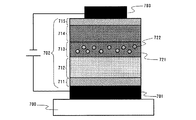
一方、本発明の基本的なコンセプトは、上述した現象を回避するために、ホール輸送層に電子吸引基を有するゲスト材料を添加し、発光層を形成した構成である。その場合のバンドダイアグラムを図2に示す。201はホール輸送層、202は電子輸送層、205はホール輸送層に電子吸引基を有するゲスト材料が添加された領域、すなわち発光層である。 On the other hand, the basic concept of the present invention is a structure in which a light emitting layer is formed by adding a guest material having an electron withdrawing group to the hole transport layer in order to avoid the above-described phenomenon. The band diagram in that case is shown in FIG. 201 is a hole transport layer, 202 is an electron transport layer, and 205 is a region where a guest material having an electron withdrawing group is added to the hole transport layer, that is, a light emitting layer.
図2のような構成の場合、電子は電子輸送層202を通過し、その後発光層205中における電子輸送層202との界面近傍203において、ゲスト材料のLUMO準位204にトラップされる。しかしながら、この構成の場合は、発光層205におけるホスト材料がホール輸送層201に用いられているホール輸送性材料であるため、図1の場合と異なり、ホールの輸送は容易である。すなわち、電子が界面近傍203でトラップされて動けなくても、ホールがその界面近傍203まで輸送されやすいため、キャリアの再結合が容易になると考えられる。その結果、図1の場合に比べて電流は流れやすくなり、駆動電圧を低減することができる。
In the case of the configuration shown in FIG. 2, electrons pass through the
なお、図2ではホール輸送層201と発光層205の両方で同じホール輸送性材料を用いた構成となっているが、異なるホール輸送性材料を用いてもよい。
In FIG. 2, the same hole transporting material is used for both the
ここで、発光層205のホスト材料として用いることができるホール輸送性材料としては、芳香族アミン骨格を有する有機化合物が好適であり、上述したα−NPDの他、4,4’−ビス[N−(3−メチルフェニル)−N−フェニル−アミノ]−ビフェニル(略称:TPD)、4,4’,4’’−トリス(N,N−ジフェニル−アミノ)−トリフェニルアミン(略称:TDATA)、4,4’,4’’−トリス[N−(3−メチルフェニル)−N−フェニル−アミノ]−トリフェニルアミン(略称:MTDATA)、4,4’,4’’−トリス[N−(1−ナフチル)−N−フェニル−アミノ]−トリフェニルアミン(略称:1−TNATA)などが挙げられる。また、芳香族アミン骨格を有する金属錯体であるトリス(5−ジフェニルアミノ−8−ヒドロキシキノリナト)アルミニウム(略称:Al(daq)3)、ビス(5−ジフェニルアミノ−8−ヒドロキシキノリナト)亜鉛(略称:Zn(daq)3)や、有機金属錯体の一種であるトリス(1−フェニルピラゾール)コバルト(III)(略称:Co(PPZ)3)、トリス(1−(4−メチルフェニル)ピラゾール)コバルト(III)(略称:Co(m−PPZ)3)などもホール輸送性を示す。
Here, as a hole transporting material that can be used as a host material of the light-emitting
一方、発光層205における電子吸引基を有するゲスト材料としては、シアノ基、ハロゲノ基、カルボニル基などの電子吸引基を有する発光材料を用いることができる。シアノ基を有する発光材料としては、例えばクマリン337の他、4−(ジシアノメチレン)−2−[p−(ジメチルアミノ)スチリル]−6−メチル−4H−ピラン(略称:DCM1)、4−(ジシアノメチレン)−2−メチル−6−(9−ジュロリジル)エチニル−4H−ピラン(略称:DCM2)、4−(ジシアノメチレン)−2,6−ビス[p−(ジメチルアミノ)スチリル]−4H−ピラン(略称:BisDCM)、先に述べたBisDCCzなどの4−ジシアノメチレン−4H−ピラン骨格を有する発光材料が挙げられる。ハロゲノ基を有する発光材料としては、クマリン152、クマリン153などのハロアルキル基を有する発光材料が代表的である。カルボニル基を有する発光材料としては、クマリン314のようにエステル基を有する発光材料、クマリン334のようにアシル基を有する発光材料、クマリン343やクマリン−3−カルボン酸のようにカルボキシル基を有する発光材料が挙げられる。
On the other hand, as the guest material having an electron-withdrawing group in the light-emitting
電子輸送層202を形成する電子輸送性材料としては、先に述べたAlq3、トリス(5−メチル−8−キノリノラト)アルミニウム(略称:Almq3)、ビス(2−メチル−8−キノリノラト)−4−フェニルフェノラト−アルミニウム(略称:BAlq)、トリス(8−キノリノラト)ガリウム(略称:Gaq3)、ビス(2−メチル−8−キノリノラト)−4−フェニルフェノラト−ガリウム(略称:BGaq)、ビス(10−ヒドロキシベンゾ[h]−キノリナト)ベリリウム略称:BeBq2)、ビス[2−(2−ヒドロキシフェニル)ベンゾオキサゾラト]亜鉛(略称:Zn(BOX)2)、ビス[2−(2−ヒドロキシフェニル)ベンゾチアゾラト]亜鉛(略称:Zn(BTZ)2)などの金属錯体が挙げられる。さらに、金属錯体以外にも、2−(4−ビフェニリル)−5−(4−tert−ブチルフェニル)−1,3,4−オキサジアゾール(略称:PBD)や、1,3−ビス[5−(p−tert−ブチルフェニル)−1,3,4−オキサジアゾール−2−イル]ベンゼン(略称:OXD−7)、3−(4−tert−ブチルフェニル)−4−フェニル−5−(4−ビフェニリル)−1,2,4−トリアゾール(略称:TAZ)、3−(4−tert−ブチルフェニル)−4−(4−エチルフェニル)−5−(4−ビフェニリル)−1,2,4−トリアゾール(略称:p−EtTAZ)、バソフェナントロリン(略称:BPhen)、バソキュプロイン(略称:BCP)等を用いることができる。
Examples of the electron transporting material that forms the
ところで、図2のような構成の場合、材料の組み合わせによっては電子輸送層202が発光してしまう可能性がある。これは、再結合領域が界面近傍203であるため、部分的にはホールが電子輸送層202に進入してしまい、電子輸送層202の材料が励起されてしまうためである。この現象が起こってしまうと、本来発光させたいゲスト材料のみならず、電子輸送層202の材料も発光してしまうため、色純度の低下を招く。
By the way, in the structure as shown in FIG. 2, the
そこで本発明のより好ましい構成の1つとして、図3のような構成が考えられる。すなわち、発光層205のホスト材料(ホール輸送性材料)のイオン化ポテンシャルと、電子輸送層202の電子輸送性材料のイオン化ポテンシャルとの差(障壁206)を大きくすればよいのである。具体的には、障壁206を0.3eV以上とすればよい。このような構成とすることで、ホールが電子輸送層202に進入する現象を防ぐことができるため、電子輸送層202の電子輸送性材料が励起されて発光してしまうという現象を抑制できる。
Therefore, as one of the more preferable configurations of the present invention, a configuration as shown in FIG. 3 can be considered. That is, the difference (barrier 206) between the ionization potential of the host material (hole transport material) of the light-emitting
障壁206を大きくするためには、発光層205のホスト材料(ホール輸送性材料)のイオン化ポテンシャルを小さくするか、あるいは電子輸送層202の電子輸送性材料のイオン化ポテンシャルを大きくすればよい。
In order to increase the
通常、多くの電子輸送性材料は5.4eV程度か、それ以上のイオン化ポテンシャルを有する(例えば、代表的な電子輸送性材料であるAlq3が5.4eVである)。したがって、ホスト材料(ホール輸送性材料)のイオン化ポテンシャルは、5.1eV以下であれば十分である。具体的には、上述したTDATA、MTDATA、1−TNATA、Al(daq)3)、Zn(daq)3などである。例えば、1−TNATAのイオン化ポテンシャルは5.0eVである。 Usually, many electron transporting materials have an ionization potential of about 5.4 eV or higher (for example, Alq 3 which is a typical electron transporting material is 5.4 eV). Therefore, it is sufficient that the ionization potential of the host material (hole transport material) is 5.1 eV or less. Specifically, the above-described TDATA, MTDATA, 1-TNATA, Al (daq) 3 ), Zn (daq) 3 and the like. For example, the ionization potential of 1-TNATA is 5.0 eV.
また逆に、多くのホール輸送性材料は5.3eV程度か、それ以下のイオン化ポテンシャルを有する(例えば、代表的なホール輸送性材料であるα−NPDが5.3eVである)。したがって、電子輸送性材料のイオン化ポテンシャルは、5.6eV以上であれば十分である。具体的には、上述したBAlq、BGaq、PBD、OXD−7、TAZ、p−EtTAZ、BPhen、BCPなどである。例えば、BAlqのイオン化ポテンシャルは5.6eVである。 Conversely, many hole transporting materials have an ionization potential of about 5.3 eV or less (for example, α-NPD which is a typical hole transporting material is 5.3 eV). Therefore, it is sufficient that the ionization potential of the electron transporting material is 5.6 eV or more. Specifically, the above-described BAlq, BGaq, PBD, OXD-7, TAZ, p-EtTAZ, BPhen, BCP, and the like. For example, the ionization potential of BAlq is 5.6 eV.
また、本発明のより好ましい他の構成として、図4のような構成も考えられる。すなわち、発光層205と電子輸送層202との間に、ホールをトラップすることができ、なおかつ、電子輸送層202を構成する電子輸送性材料よりもエネルギーギャップの値が小さいホールトラップ材料からなるホールトラップ領域207を設ける構成である。このような構成とすることで、ホールが電子輸送層202に進入する現象を防ぐことができ、しかもホールトラップ材料が励起されたとしても、その励起エネルギーが電子輸送層202の電子輸送性材料へ移動してしまう現象を防ぐことができる。したがって、電子輸送層202の電子輸送性材料が励起されて発光してしまうという現象を抑制できる。
Further, as another preferred configuration of the present invention, a configuration as shown in FIG. 4 is also conceivable. That is, a hole made of a hole trap material that can trap holes between the light emitting
ホールトラップ材料としては、発光層205のホスト材料および電子輸送層202の電子輸送性材料よりも小さいイオン化ポテンシャルを有するものを用いれば、図4中の矢印で示したように効果的にホールをトラップすることができる。ただし、必ずしもこのような構成になっていなくても、ホールが電子輸送層202に進入するのを防ぎ、電子輸送層202の電子輸送性材料が発光するのを抑制できる材料であれば、ホールトラップ材料となり得る。ホールトラップ材料の具体的な例としては、テトラセン、ペンタセン、ペリレン、コロネン、ルブレン等に代表される炭素数が18以上の芳香族炭化水素化合物が、イオン化ポテンシャルが小さく好適である。また、フラーレン(C60)やカーボンナノチューブ、ダイヤモンドライクカーボン(略称:DLC)などの炭素同素体は、エネルギーギャップが小さく好適である。
If a hole trap material having a smaller ionization potential than the host material of the
また、ホールトラップ領域があまりに厚い場合は、ホールトラップ材料の材質によっては電子の流れを妨げたり、あるいはホールトラップ材料自体が励起されて発光してしまうなどの弊害が生じやすくなる。特に、ホールトラップ材料が発光してしまう弊害を避けるためには、ホールトラップ材料からゲスト材料へのフェルスター型のエネルギー移動が十分に可能な距離を考慮し、ホールトラップ領域が5nm以下の層状であることが好ましい。 If the hole trap region is too thick, depending on the material of the hole trap material, the electron flow may be hindered, or the hole trap material itself may be excited to emit light. In particular, in order to avoid the adverse effect of the hole trap material emitting light, the hole trap region has a layer thickness of 5 nm or less in consideration of the distance at which the Forster type energy transfer from the hole trap material to the guest material is sufficiently possible. Preferably there is.
また、5nm以下という観点から、ホールトラップ領域は層状ではなく島状に形成されていてもよい。島状の構造の形成法としては公知の手法を用いればよく、例えば特開2001−267077に開示されているように、膜厚モニター上の平均膜厚が単分子膜の膜厚より薄くなるように材料を真空蒸着する手法が挙げられる。 Further, from the viewpoint of 5 nm or less, the hole trap region may be formed in an island shape instead of a layer shape. As a method for forming the island structure, a known method may be used. For example, as disclosed in JP-A-2001-267077, the average film thickness on the film thickness monitor is made smaller than the film thickness of the monomolecular film. The method of vacuum-depositing a material is mentioned.
ところで、先に述べたとおり、電子吸引基を有する赤色発光のゲスト材料をホスト材料に添加して発光層を形成し、赤色発光素子を作製する際に、双極子モーメントの小さいホスト材料を使うと、双極子モーメントの大きいホスト材料を使う場合に比べて発光がブルーシフトしてしまい、場合によっては色純度のよい赤色が達成できないこともある。これは溶媒効果の一種であると考えられる。 By the way, as described above, when a red light emitting guest material having an electron withdrawing group is added to a host material to form a light emitting layer and a red light emitting element is manufactured, a host material having a small dipole moment is used. As compared with the case of using a host material having a large dipole moment, the light emission is blue-shifted, and in some cases, red with good color purity may not be achieved. This is considered to be a kind of solvent effect.
従来ホスト材料として用いられているAlq3には2種類の構造異性体があり、通常はfac型と言われている。そして、その双極子モーメントを市販の分子軌道計算プログラムWinMOPAC3.5(富士通株式会社製)を用いて計算したところ、9.398デバイであった(ちなみに、もう一つの構造異性体であるmer型の双極子モーメントは、5.788デバイである)。Alq3をホスト材料として電子吸引基を有する赤色発光のゲスト材料を添加した素子は、駆動電圧は上昇するが、双極子モーメントのより小さい材料(具体的には4デバイよりも小さい材料)をホスト材料として用いた素子に比べ、発光色としては良好な赤色発光を示すことが実験的にわかっている。 Alq 3 conventionally used as a host material has two types of structural isomers and is usually referred to as fac type. The dipole moment was calculated using a commercially available molecular orbital calculation program WinMOPAC3.5 (manufactured by Fujitsu Limited) and found to be 9.398 debye (by the way, another structural isomer of mer type The dipole moment is 5.788 debye). A device in which a guest material that emits red light having an electron-attracting group with Alq 3 as a host material is added to a material that has a higher dipole moment but has a smaller dipole moment (specifically, a material that is smaller than 4 debyes). It has been experimentally found that the device emits red light better than the element used as the material.
このことから、色純度のよい赤色発光を達成するためには、ホスト材料の双極子モーメントの大きさが重要であることがわかる。しかしながら、Alq3は電子輸送性材料であるため、本発明におけるホスト材料としては適さない。 This indicates that the magnitude of the dipole moment of the host material is important in order to achieve red light emission with good color purity. However, since Alq 3 is an electron transporting material, it is not suitable as a host material in the present invention.
したがって、本発明を用いて赤色発光素子を作製する場合には、Alq3のように双極子モーメントが大きく、なおかつホール輸送性を示す材料を用いることが好ましい。通常の芳香族アミン骨格を有する有機化合物の多くは双極子モーメントが小さいが、上述したAl(daq)3、Zn(daq)3、Co(PPZ)3、Co(m−PPZ)3のようなホール輸送性を示す金属錯体であれば、双極子モーメントが大きく好適である。例えば、Al(daq)3の双極子モーメントを計算したところ、fac型では9.221デバイであった(ちなみに、もう一つの構造異性体であるmer型の双極子モーメントは、4.639デバイである)。 Therefore, when a red light emitting element is manufactured using the present invention, it is preferable to use a material having a large dipole moment and exhibiting hole transport properties such as Alq 3 . Many organic compounds having a normal aromatic amine skeleton have a small dipole moment, but such as Al (daq) 3 , Zn (daq) 3 , Co (PPZ) 3 , and Co (m-PPZ) 3 described above. A metal complex exhibiting hole transport properties is suitable because of its large dipole moment. For example, when the dipole moment of Al (daq) 3 was calculated, it was 9.221 debye for the fac type (by the way, the dipole moment of the mer type which is another structural isomer is 4.639 debye). is there).
したがって本発明では、上述した構成の電界発光素子において、ゲスト材料の発光スペクトルのピーク波長が600nm以上700nm以下の赤色領域に存在する時には、ホスト材料の分子の双極子モーメントが4デバイ以上であることが好ましい。 Therefore, in the present invention, when the peak wavelength of the emission spectrum of the guest material is in the red region of 600 nm or more and 700 nm or less in the electroluminescent element having the above-described configuration, the dipole moment of the molecule of the host material is 4 Debye or more. Is preferred.
次に、以下では、本発明の電界発光素子の実施形態について詳細に説明する。本発明の電界発光素子の電界発光層は、少なくとも上述した発光層と電子輸送層とを含めばよい。すなわち、従来の電界発光素子で知られているような、発光以外の機能を示す層(ホール注入層、ホール輸送層、電子輸送層、電子注入層)を適宜組み合わせてもよい。 Next, embodiments of the electroluminescent element of the present invention will be described in detail below. The electroluminescent layer of the electroluminescent element of the present invention may include at least the above-described light emitting layer and electron transport layer. That is, layers (hole injection layer, hole transport layer, electron transport layer, electron injection layer) showing functions other than light emission as known in conventional electroluminescent elements may be appropriately combined.
[実施の形態1]
本実施の形態1では、ホール注入層、ホール輸送層、発光層、電子輸送層および電子注入層を有する電界発光素子の素子構成について、図5を用いて説明する。図5は、基板500上に第1の電極501が形成され、第1の電極501上に電界発光層502が形成され、その上に第2の電極503が形成された電界発光素子である。
[Embodiment 1]
In Embodiment 1, an element structure of an electroluminescent element having a hole injection layer, a hole transport layer, a light emitting layer, an electron transport layer, and an electron injection layer will be described with reference to FIG. FIG. 5 illustrates an electroluminescent element in which a
なお、ここで基板500に用いる材料としては、従来の電界発光素子に用いられているものであればよく、例えば、ガラス、石英、透明プラスチックなどからなるものを用いることができる。
In addition, as a material used for the board |
また、本実施の形態1における第1の電極501は陽極として機能し、第2の電極503は陰極として機能する。
In the first embodiment, the
すなわち第1の電極501は陽極材料で形成され、仕事関数の大きい(具体的には4.0eV以上)金属、合金、導電性化合物、およびこれらの混合物などを用いることが好ましい。具体的には、ITO(indium tin oxide)、酸化インジウムに2〜20[%]の酸化亜鉛(ZnO)を混合したIZO(indium zinc oxide)の他、金(Au)、白金(Pt)、ニッケル(Ni)、タングステン(W)、クロム(Cr)、モリブデン(Mo)、鉄(Fe)、コバルト(Co)、銅(Cu)、パラジウム(Pd)、または金属材料の窒化物(TiN)等が挙げられる。
That is, the
一方、第2の電極503に用いられる陰極材料としては、仕事関数の小さい(具体的には3.8eV以下)金属、合金、導電性化合物、およびこれらの混合物などを用いることが好ましい。具体的には、元素周期律の1族または2族に属する金属、すなわちLiやCs等のアルカリ金属、およびMg、Ca、Sr等のアルカリ土類金属、およびこれらを含む合金(Mg:Ag、Al:Li)、Er、Yb等の希土類金属およびこれらを含む合金等が挙げられる。ただし、後述する電子注入層を適用することで、Al、Ag、ITO等の金属・導電性無機化合物により第2の電極503を形成することもできる。
On the other hand, as the cathode material used for the
なお、第1の電極501及び第2の電極503は、蒸着法、スパッタリング法等で形成することができる。膜厚は、10〜500nmとするのが好ましい。
Note that the
また、本発明の電界発光素子において、電界発光層502におけるキャリアの再結合により生じる光は、第1の電極501または第2の電極503の一方、または両方から外部に出射される構成となる。すなわち、第1の電極501から光を出射させる場合には、第1の電極501を透光性の材料で形成することとし、第2の電極503側から光を出射させる場合には、第2の電極503を透光性の材料で形成することとする。
In the electroluminescent element of the present invention, light generated by recombination of carriers in the
電界発光層502は複数の層を積層することにより形成されるが、本実施の形態1では、ホール注入層511、ホール輸送層512、発光層513、電子輸送層514、電子注入層515を積層することにより形成される。これらの層は、真空蒸着法や湿式塗布法で形成することができる。
The
ホール注入層511に用いることができるホール注入性材料としては、有機化合物であればポルフィリン系の化合物が有効であり、フタロシアニン(略称:H2−Pc)、銅フタロシアニン(略称:Cu−Pc)等を用いることができる。他にも、有機化合物としては、4,4’−ビス[N−{4−(N,N−ビス(3−メチルフェニル)アミノ)フェニル}−N−フェニルアミノ]ビフェニル(略称:DNTPD)等を用いることができる。また、導電性高分子化合物に化学ドーピングを施した材料もあり、ポリスチレンスルホン酸(略称:PSS)をドープしたポリエチレンジオキシチオフェン(略称:PEDOT)や、ポリアニリン(略称:PAni)などを用いることもできる。また、VOx、MoOxのような無機半導体層や、Al2O3などの無機絶縁体の超薄膜も有効である。
As a hole-injecting material that can be used for the hole-injecting
ホール輸送層512に用いることができるホール輸送性材料としては、先に述べたα−NPD、TPD、TDATA、MTDATA、1−TNATA、Al(daq)3、Zn(daq)3、Co(PPZ)3、Co(m−PPZ)3などが挙げられる。
Examples of the hole transporting material that can be used for the
発光層513は、ホール輸送性を示すホスト材料521と電子吸引基を有するゲスト材料522から構成されている。ホール輸送性を示すホスト材料521としては、上述のホール輸送性材料を適用すればよく、ホール輸送層512のホール輸送性材料と同一であっても異なっていてもよい。電子吸引基を有するゲスト材料としては、先に述べたDCM1、DCM2、BisDCM、BisDCCz、クマリン337、クマリン152、クマリン153、クマリン314、クマリン334、クマリン343、クマリン−3−カルボン酸などが挙げられる。
The light-emitting
電子輸送層514に用いることができる電子輸送性材料としては、先に述べたAlq3、Almq3、BAlq、Gaq3、BGaq、BeBq2、Zn(BOX)2、Zn(BTZ)2、PBD、OXD−7、TAZ、p−EtTAZ、BPhen、BCPなどが挙げられる。
Examples of the electron transporting material that can be used for the
電子注入層515に用いることができる電子注入性材料としては、上述した電子輸送性材料を用いることができる。その他に、LiF、CsFなどのアルカリ金属ハロゲン化物や、CaF2のようなアルカリ土類ハロゲン化物、Li2Oなどのアルカリ金属酸化物のような絶縁体の超薄膜がよく用いられる。また、リチウムアセチルアセトネート(略称:Li(acac)や8−キノリノラト−リチウム(略称:Liq)などのアルカリ金属錯体も有効である。さらに、上述した電子輸送性材料と、Mg、Li、Cs等の仕事関数の小さい金属とを混合した層を電子注入層515として使用することもできる。
As the electron injecting material that can be used for the
以上により、ホール輸送性を有するホスト材料521および電子吸引基を有するゲスト材料522を含む発光層513と、発光層513に接して設けられた電子輸送層514とを有する本発明の電界発光素子を作製することができる。
As described above, the electroluminescent element of the present invention including the light-emitting
[実施の形態2]
本実施の形態2では、実施の形態1で開示した素子構成にホールトラップ領域を加えた構成について、図6を用いて説明する。図6では、図5の符号を引用する。
[Embodiment 2]
In Embodiment 2, a structure in which a hole trap region is added to the element structure disclosed in Embodiment 1 will be described with reference to FIGS. In FIG. 6, the reference numerals of FIG. 5 are cited.
図6に示す通り、本実施の形態2においては、発光層513と電子輸送層514との間にホールトラップ領域516が設けられている。図6では島状に形成されているが、5nm以下の層状であってもよい。
As shown in FIG. 6, in the second embodiment, a
ホールトラップ領域516を構成するホールトラップ材料523としては、先に述べたように、テトラセン、ペンタセン、ペリレン、コロネン、ルブレン、フラーレン(C60)、カーボンナノチューブ、DLCなどを用いることができる。
As the
以上により、ホール輸送性を有するホスト材料521および電子吸引基を有するゲスト材料522を含む発光層513と、発光層513に接して設けられた電子輸送層514とを有し、かつ、発光層513と電子輸送層514との間にホールトラップ領域516を設けた本発明の電界発光素子を作製することができる。この構成により、電子輸送層514の電子輸送性材料が発光してしまう現象を抑制することができる。
As described above, the light-emitting
本実施例1では、図5で示した本発明の電界発光素子の作製例を、具体的に例示する。 In Example 1, an example of manufacturing the electroluminescent element of the present invention shown in FIG. 5 is specifically illustrated.
まず、絶縁表面を有するガラス基板500上に、第1の電極(陽極)501が形成される。材料として透明導電膜であるITOを用い、スパッタリング法により110nmの膜厚で形成した。陽極501の形状は、2mm×2mmの大きさとした。
First, a first electrode (anode) 501 is formed over a
このように陽極501が形成された基板を洗浄、乾燥した後、陽極501上に電界発光層502を形成する。まず、陽極501が形成された基板を、真空蒸着装置の基板ホルダーに陽極501が形成された面を下方にして固定し、抵抗加熱法を用いた真空蒸着法によりCu−Pcを20nmの膜厚で成膜した。これがホール注入層511となる。次に、ホール輸送性材料であるα−NPDを同様の方法により、25nmの膜厚で形成し、ホール輸送層512とした。
After the substrate on which the
さらに、ホスト材料521としてホール輸送性材料であるα−NPDを、電子吸引基を有するゲスト材料522としてBisDCMを用い、BisDCMの濃度が2wt%となるように共蒸着を行うことで発光層513を形成した。膜厚は15nmとした。
Further, α-NPD which is a hole transporting material is used as the
次に、電子輸送性材料であるAlq3を真空蒸着法により75nm形成し、電子輸送層514とした。さらに、電子注入層515として、CaF2を真空蒸着法により1nm形成した。以上が電界発光層502であり、トータル膜厚は136nmとなる。
Next, Alq 3 which is an electron transporting material was formed to have a thickness of 75 nm by a vacuum evaporation method, and an
最後に、第2の電極(陰極)503を形成する。本実施例では、アルミニウム(Al)を抵抗加熱による真空蒸着法により200nm形成し、陰極503とした。
Finally, a second electrode (cathode) 503 is formed. In this example, aluminum (Al) was formed to 200 nm by a vacuum evaporation method using resistance heating to form a
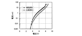
以上のようにして作製した本発明の電界発光素子に10Vの電圧を印加したところ、6.83mA/cm2の電流密度で電流が流れ、127cd/m2の輝度で発光した。発光スペクトルのピーク波長は642nmであった。 When a voltage of 10 V was applied to the electroluminescent device of the present invention produced as described above, a current flowed at a current density of 6.83 mA / cm 2 , and light was emitted with a luminance of 127 cd / m 2 . The peak wavelength of the emission spectrum was 642 nm.
[比較例1]
一方、電子輸送性材料に電子吸引基を有するゲスト材料を添加した発光層を有する従来の電界発光素子を作製し、実施例1と比較した。本比較例の素子構造を図7に示す。
[Comparative Example 1]
On the other hand, a conventional electroluminescent device having a light emitting layer in which a guest material having an electron withdrawing group was added to an electron transporting material was manufactured and compared with Example 1. The element structure of this comparative example is shown in FIG.
上記実施例1と同様に、110nmのITOが陽極701として形成されたガラス基板700上に、電界発光層702を形成する。まず、基板を洗浄、乾燥した後、真空蒸着装置の基板ホルダーに陽極701が形成された面を下方にして固定し、抵抗加熱法を用いた真空蒸着法によりCu−Pcを20nmの膜厚で成膜した。これがホール注入層711となる。次に、ホール輸送性材料であるα−NPDを同様の方法により、40nmの膜厚で形成し、ホール輸送層712とした。
Similar to Example 1, an
さらに、ホスト材料721として電子輸送性材料であるAlq3を、電子吸引基を有するゲスト材料722として実施例1と同じBisDCMを用い、BisDCMの濃度が2wt%となるように共蒸着を行うことで発光層713を形成した。膜厚は15nmとした。
Further, Alq 3 which is an electron transporting material is used as the
次に、電子輸送性材料であるAlq3を真空蒸着法により60nm形成し、電子輸送層714とした。さらに、電子注入層715として、CaF2を真空蒸着法により1nm形成した。以上が電界発光層702であるが、トータル膜厚は136nmであり、実施例1と膜厚を揃えてある。
Next, Alq 3 which is an electron transporting material was formed to a thickness of 60 nm by a vacuum evaporation method, and an
最後に、陰極703を形成する。実施例1と同様、アルミニウム(Al)を抵抗加熱による真空蒸着法により200nm形成し、陰極703とした。
Finally, the
以上のようにして作製した従来の電界発光素子に10Vの電圧を印加したところ、2.84mA/cm2の電流密度で電流が流れ、27.1cd/m2の輝度で発光した。発光スペクトルのピーク波長は666nmであった。 When a voltage of 10 V was applied to the conventional electroluminescent device fabricated as described above, a current flowed at a current density of 2.84 mA / cm 2 , and light was emitted with a luminance of 27.1 cd / m 2 . The peak wavelength of the emission spectrum was 666 nm.
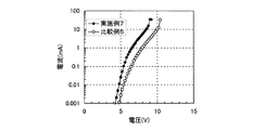
上述の結果から、本発明を適用した電界発光素子は、発光スペクトルのピーク波長が若干ブルーシフトしているものの、駆動電圧を下げることができた。実施例1および比較例1の電流−電圧特性を図10に示す。図10からわかるように、本発明を適用することで、狙い通り電流が流れやすくなっていることがわかる。 From the above results, the electroluminescent device to which the present invention was applied was able to lower the driving voltage, although the peak wavelength of the emission spectrum was slightly blue shifted. The current-voltage characteristics of Example 1 and Comparative Example 1 are shown in FIG. As can be seen from FIG. 10, it can be seen that by applying the present invention, the current easily flows as intended.
本実施例2では、実施例1とは異なるホスト材料を用いた素子を具体的に例示する。 In Example 2, an element using a host material different from that in Example 1 is specifically illustrated.
素子構造は図5に示した構造であり、基板500、陽極501、陰極503は実施例1と同様の構成とした。電界発光層502は、ホール注入層511としてCuPcを20nm、ホール輸送層512としてα−NPDを30nm、発光層513として2,3−ビス(4−ジフェニルアミノフェニル)キノキサリン(略称:TPAQn)に1wt%の割合でBisDCMを添加した層を30nm、電子輸送層としてAlq3を20nm、電子注入層としてCaF2を2nm形成した。トータル膜厚は102nmである。なお、TPAQnはバイポーラな材料であるため、ホール輸送性を有する。
The element structure is the structure shown in FIG. 5, and the
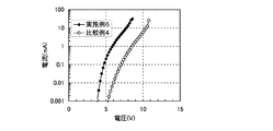
以上のようにして作製した本発明の電界発光素子に10Vの電圧を印加したところ、283mA/cm2の電流密度で電流が流れ、1350cd/m2の輝度で発光した。発光スペクトルのピーク波長は616nmであった。 When a voltage of 10 V was applied to the electroluminescent device of the present invention produced as described above, a current flowed at a current density of 283 mA / cm 2 , and light was emitted with a luminance of 1350 cd / m 2 . The peak wavelength of the emission spectrum was 616 nm.
[比較例2]
一方、電子輸送性材料に電子吸引基を有するゲスト材料を添加した発光層を有する従来の電界発光素子を作製し、実施例2と比較した。本比較例の素子構造は図7と同様とした。
[Comparative Example 2]
On the other hand, a conventional electroluminescent device having a light emitting layer in which a guest material having an electron withdrawing group was added to an electron transporting material was manufactured and compared with Example 2. The element structure of this comparative example was the same as that shown in FIG.
上記実施例2と同様に、基板700、陽極701、陰極703は上述した実施例2と全く同一とした。電界発光層702は、ホール注入層711としてCuPcを20nm、ホール輸送層712としてα−NPDを30nm、発光層713として電子輸送性材料であるBAlに1wt%の割合でBisDCMを添加した層を30nm、電子輸送層としてAlq3を20nm、電子注入層としてCaF2を2nm形成した。トータル膜厚は102nmであり、実施例2と同じである。
As in the second embodiment, the
以上のようにして作製した従来の電界発光素子に10Vの電圧を印加したところ、4.23mA/cm2の電流密度で電流が流れ、30.9cd/m2の輝度で発光した。発光スペクトルのピーク波長は619nmであった。 When a voltage of 10 V was applied to the conventional electroluminescent device fabricated as described above, current flowed at a current density of 4.23 mA / cm 2 , and light was emitted with a luminance of 30.9 cd / m 2 . The peak wavelength of the emission spectrum was 619 nm.
上述の結果から、本発明を適用した電界発光素子は、発光スペクトルのピーク波長が従来とほぼ同様であり、なおかつ駆動電圧を下げることができた。実施例2および比較例2の電流−電圧特性を図11に示す。図11からわかるように、本発明を適用することで、狙い通り電流が流れやすくなっていることがわかる。 From the above results, the electroluminescence device to which the present invention is applied has the peak wavelength of the emission spectrum substantially the same as the conventional one, and the driving voltage can be lowered. The current-voltage characteristics of Example 2 and Comparative Example 2 are shown in FIG. As can be seen from FIG. 11, by applying the present invention, it can be seen that the current easily flows as intended.
本実施例では、画素部に本発明の電界発光素子を有する発光装置について図8を用いて説明する。なお、図8(A)は、発光装置を示す上面図、図8(B)は図8(A)をA−A’で切断した断面図である。点線で示された801は駆動回路部(ソース側駆動回路)、802は画素部、803は駆動回路部(ゲート側駆動回路)である。また、804は封止基板、805はシール材であり、シール材805で囲まれた内側は、空間807になっている。 In this embodiment, a light-emitting device having the electroluminescent element of the present invention in a pixel portion will be described with reference to FIG. 8A is a top view illustrating the light-emitting device, and FIG. 8B is a cross-sectional view taken along line A-A ′ in FIG. 8A. Reference numeral 801 indicated by a dotted line denotes a drive circuit portion (source side drive circuit), 802 denotes a pixel portion, and 803 denotes a drive circuit portion (gate side drive circuit). Further, reference numeral 804 denotes a sealing substrate, and 805 denotes a sealing material. An inner side surrounded by the sealing material 805 is a space 807.
なお、808はソース側駆動回路801及びゲート側駆動回路803に入力される信号を伝送するための配線であり、外部入力端子となるFPC(フレキシブルプリントサーキット)809からビデオ信号、クロック信号、スタート信号、リセット信号等を受け取る。なお、ここではFPCしか図示されていないが、このFPCにはプリント配線基盤(PWB)が取り付けられていても良い。本明細書における発光装置には、発光装置本体だけでなく、それにFPCもしくはPWBが取り付けられた状態をも含むものとする。 Reference numeral 808 denotes a wiring for transmitting signals input to the source side driver circuit 801 and the gate side driver circuit 803, and a video signal, a clock signal, and a start signal from an FPC (flexible printed circuit) 809 serving as an external input terminal. Receive a reset signal, etc. Although only the FPC is shown here, a printed wiring board (PWB) may be attached to the FPC. The light-emitting device in this specification includes not only a light-emitting device body but also a state in which an FPC or a PWB is attached thereto.
次に、断面構造について図8(B)を用いて説明する。素子基板810上には駆動回路部及び画素部が形成されているが、ここでは、駆動回路部であるソース側駆動回路801と、画素部802が示されている。 Next, a cross-sectional structure is described with reference to FIG. A driver circuit portion and a pixel portion are formed over the element substrate 810. Here, a source side driver circuit 801 which is a driver circuit portion and a pixel portion 802 are shown.
なお、ソース側駆動回路801はnチャネル型TFT823とpチャネル型TFT824とを組み合わせたCMOS回路が形成される。また、駆動回路を形成するTFTは、公知のCMOS回路、PMOS回路もしくはNMOS回路で形成しても良い。また、本実施の形態では、基板上に駆動回路を形成したドライバー一体型を示すが、必ずしもその必要はなく、基板上ではなく外部に形成することもできる。 Note that the source side driver circuit 801 is a CMOS circuit in which an n-channel TFT 823 and a p-channel TFT 824 are combined. The TFT forming the driving circuit may be formed by a known CMOS circuit, PMOS circuit or NMOS circuit. In this embodiment mode, a driver integrated type in which a driver circuit is formed over a substrate is shown; however, this is not always necessary, and the driver circuit may be formed outside the substrate.
また、画素部802はスイッチング用TFT811と、電流制御用TFT812とそのドレインに電気的に接続された第1の電極813とを含む複数の画素により形成される。なお、第1の電極813の端部を覆って絶縁物814が形成されている。ここでは、ポジ型の感光性アクリル樹脂膜を用いることにより形成する。 The pixel portion 802 is formed of a plurality of pixels including a switching TFT 811, a current control TFT 812, and a first electrode 813 electrically connected to the drain thereof. Note that an insulator 814 is formed to cover an end portion of the first electrode 813. Here, a positive photosensitive acrylic resin film is used.
また、カバレッジを良好なものとするため、絶縁物814の上端部または下端部に曲率を有する曲面が形成されるようにする。例えば、絶縁物814の材料としてポジ型の感光性アクリルを用いた場合、絶縁物814の上端部のみに曲率半径(0.2μm〜3μm)を有する曲面を持たせることが好ましい。また、絶縁物814として、感光性の光によってエッチャントに不溶解性となるネガ型、或いは光によってエッチャントに溶解性となるポジ型のいずれも使用することができる。 In order to improve the coverage, a curved surface having a curvature is formed at the upper end portion or the lower end portion of the insulator 814. For example, in the case where positive photosensitive acrylic is used as a material for the insulator 814, it is preferable that only the upper end portion of the insulator 814 have a curved surface having a curvature radius (0.2 μm to 3 μm). As the insulator 814, either a negative type that becomes insoluble in an etchant by photosensitive light or a positive type that becomes soluble in an etchant by light can be used.
第1の電極813上には、電界発光層816、および第2の電極817がそれぞれ形成されている。ここで、陽極として機能する第1の電極813に用いる材料としては、仕事関数の大きい材料を用いることが望ましい。例えば、ITO(インジウムスズ酸化物)膜、インジウム亜鉛酸化物(IZO)膜、窒化チタン膜、クロム膜、タングステン膜、Zn膜、Pt膜などの単層膜の他、窒化チタンとアルミニウムを主成分とする膜との積層、窒化チタン膜とアルミニウムを主成分とする膜と窒化チタン膜との3層構造等を用いることができる。なお、積層構造とすると、配線としての抵抗も低く、良好なオーミックコンタクトがとれ、さらに陽極として機能させることができる。 An electroluminescent layer 816 and a second electrode 817 are formed over the first electrode 813, respectively. Here, as a material used for the first electrode 813 functioning as an anode, a material having a high work function is preferably used. For example, ITO (Indium Tin Oxide) film, Indium Zinc Oxide (IZO) film, Titanium nitride film, Chromium film, Tungsten film, Zn film, Pt film, etc., as well as titanium nitride and aluminum as main components And a three-layer structure of a titanium nitride film, a film containing aluminum as its main component, and a titanium nitride film can be used. Note that with a stacked structure, resistance as a wiring is low, good ohmic contact can be obtained, and a function as an anode can be obtained.
また、電界発光層816は、蒸着マスクを用いた蒸着法、またはインクジェット法によって形成される。電界発光層816の構成は、例えば実施例1や実施例2で示した電界発光層の構成とすればよい。 The electroluminescent layer 816 is formed by an evaporation method using an evaporation mask or an inkjet method. The configuration of the electroluminescent layer 816 may be the configuration of the electroluminescent layer shown in Example 1 or Example 2, for example.
さらに、電界発光層816上に形成される第2の電極(陰極)817に用いる材料としては、仕事関数の小さい材料(Al、Ag、Li、Ca、またはこれらの合金MgAg、MgIn、AlLi、CaF2、またはCaN)を用いればよい。なお、電界発光層816で生じた光が第2の電極817を透過させる場合には、第2の電極(陰極)817として、例えば、膜厚を薄くした金属薄膜と、透明導電膜(ITO、IZO、酸化亜鉛(ZnO)等)との積層を用いる方法などがある。 Further, as a material used for the second electrode (cathode) 817 formed on the electroluminescent layer 816, a material having a low work function (Al, Ag, Li, Ca, or alloys thereof MgAg, MgIn, AlLi, CaF) is used. 2 or CaN). Note that in the case where light generated in the electroluminescent layer 816 is transmitted through the second electrode 817, as the second electrode (cathode) 817, for example, a thin metal film and a transparent conductive film (ITO, And a method using a stack with IZO, zinc oxide (ZnO), or the like.
さらにシール材805で封止基板804を素子基板810と貼り合わせることにより、素子基板810、封止基板804、およびシール材805で囲まれた空間807に電界発光素子818が備えられた構造になっている。なお、空間807には、不活性気体(窒素やアルゴン等)が充填される場合の他、シール材805で充填される構成も含むものとする。 Further, the sealing substrate 804 is bonded to the element substrate 810 with the sealant 805, whereby the electroluminescent element 818 is provided in the space 807 surrounded by the element substrate 810, the sealing substrate 804, and the sealant 805. ing. Note that the space 807 includes a structure filled with a sealant 805 in addition to a case where the space is filled with an inert gas (nitrogen, argon, or the like).
なお、シール材805にはエポキシ系樹脂を用いるのが好ましい。また、これらの材料はできるだけ水分や酸素を透過しない材料であることが望ましい。また、封止基板804に用いる材料としてガラス基板や石英基板の他、FRP(Fiberglass−Reinforced Plastics)、PVF(ポリビニルフロライド)、マイラー、ポリエステルまたはアクリル等からなるプラスチック基板を用いることができる。 Note that an epoxy-based resin is preferably used for the sealant 805. Moreover, it is desirable that these materials are materials that do not transmit moisture and oxygen as much as possible. In addition to a glass substrate and a quartz substrate, a plastic substrate made of FRP (Fiberglass-Reinforced Plastics), PVF (polyvinyl fluoride), Mylar, polyester, acrylic, or the like can be used as a material used for the sealing substrate 804.
以上のようにして、本発明の電界発光素子を有する発光装置を得ることができる。 As described above, a light-emitting device having the electroluminescent element of the present invention can be obtained.
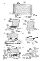
例えば、本発明の電界発光素子を有する発光装置を表示部として有する様々な電気器具を提供することができる。 For example, various electric appliances including a light-emitting device having the electroluminescent element of the present invention as a display portion can be provided.
本発明の電界発光素子を有する発光装置を用いて作製された電気器具として、ビデオカメラ、デジタルカメラ、ゴーグル型ディスプレイ、ナビゲーションシステム、音響再生装置(カーオーディオ、オーディオコンポ等)、ノート型パーソナルコンピュータ、ゲーム機器、携帯情報端末(モバイルコンピュータ、携帯電話、携帯型ゲーム機または電子書籍等)、記録媒体を備えた画像再生装置(具体的にはDigital Versatile Disc(DVD)等の記録媒体を再生し、その画像を表示しうる表示装置を備えた装置)などが挙げられる。これらの電気器具の具体例を図9に示す。 As an electric appliance manufactured using a light emitting device having an electroluminescent element of the present invention, a video camera, a digital camera, a goggle type display, a navigation system, an acoustic reproduction device (car audio, audio component, etc.), a notebook personal computer, Reproducing a recording medium such as a game machine, a portable information terminal (mobile computer, cellular phone, portable game machine, electronic book, etc.), an image reproducing apparatus (specifically, Digital Versatile Disc (DVD)) equipped with a recording medium, A device provided with a display device capable of displaying the image). Specific examples of these electric appliances are shown in FIG.
図9(A)は表示装置であり、筐体9101、支持台9102、表示部9103、スピーカー部9104、ビデオ入力端子9105等を含む。本発明の電界発光素子を有する発光装置をその表示部9103に用いることにより作製される。なお、表示装置は、コンピュータ用、TV放送受信用、広告表示用などの全ての情報表示用装置が含まれる。
FIG. 9A illustrates a display device, which includes a
図9(B)はノート型パーソナルコンピュータであり、本体9201、筐体9202、表示部9203、キーボード9204、外部接続ポート9205、ポインティングマウス9206等を含む。本発明の電界発光素子を有する発光装置をその表示部9203に用いることにより作製される。
FIG. 9B shows a laptop personal computer, which includes a
図9(C)はモバイルコンピュータであり、本体9301、表示部9302、スイッチ9303、操作キー9304、赤外線ポート9305等を含む。本発明の電界発光素子を有する発光装置をその表示部9302に用いることにより作製される。
FIG. 9C illustrates a mobile computer, which includes a
図9(D)は記録媒体を備えた携帯型の画像再生装置(具体的にはDVD再生装置)であり、本体9401、筐体9402、表示部A9403、表示部B9404、記録媒体(DVD等)読み込み部9405、操作キー9406、スピーカー部9407等を含む。表示部A9403は主として画像情報を表示し、表示部B9404は主として文字情報を表示するが、本発明の電界発光素子を有する発光装置をこれら表示部A9403、B9404に用いることにより作製される。なお、記録媒体を備えた画像再生装置には家庭用ゲーム機器なども含まれる。
FIG. 9D illustrates a portable image reproducing device (specifically, a DVD reproducing device) provided with a recording medium, which includes a
図9(E)はゴーグル型ディスプレイであり、本体9501、表示部9502、アーム部9503を含む。本発明の電界発光素子を有する発光装置をその表示部9502に用いることにより作製される。
FIG. 9E illustrates a goggle type display, which includes a
図9(F)はビデオカメラであり、本体9601、表示部9602、筐体9603、外部接続ポート9604、リモコン受信部9605、受像部9606、バッテリー9607、音声入力部9608、操作キー9609、接眼部9610等を含む。本発明の電界発光素子を有する発光装置をその表示部9602に用いることにより作製される。
FIG. 9F illustrates a video camera, which includes a main body 9601, a display portion 9602, a
ここで、図9(G)は携帯電話であり、本体9701、筐体9702、表示部9703、音声入力部9704、音声出力部9705、操作キー9706、外部接続ポート9707、アンテナ9708等を含む。本発明の電界発光素子を有する発光装置をその表示部9703に用いることにより作製される。なお、表示部9703は黒色の背景に白色の文字を表示することで携帯電話の消費電力を抑えることができる。
Here, FIG. 9G shows a cellular phone, which includes a
本実施例5では、実施例1、2とは異なる電子吸引基を有するゲスト材料を用いた電界発光素子の作製例を、具体的に例示する。素子構造は図5の通りとした。 In Example 5, an example of manufacturing an electroluminescent element using a guest material having an electron-withdrawing group different from those in Examples 1 and 2 is specifically illustrated. The element structure was as shown in FIG.
まず、絶縁表面を有するガラス基板500上に、陽極501が形成される。材料として酸化ケイ素を添加したインジウム錫酸化物(ITSO)を用い、スパッタリング法により110nmの膜厚で形成した。陽極501の形状は、2mm×2mmの大きさとした。
First, the
このように陽極501が形成された基板を洗浄、乾燥した後、陽極501上に電界発光層502を形成する。まず、陽極501が形成された基板を、真空蒸着装置の基板ホルダーに陽極501が形成された面を下方にして固定し、抵抗加熱法を用いた真空蒸着法により4,4’−ビス[N−[4−{N,N−ビス(3−メチルフェニル)アミノ}フェニル]−N−フェニルアミノ]ビフェニル(略称:DNTPD)を50nmの膜厚で成膜した。これがホール注入層511となる。次に、ホール輸送性材料であるα−NPDを同様の方法により、10nmの膜厚で形成し、ホール輸送層512とした。
After the substrate on which the
さらに、ホスト材料521としてホール輸送性材料であるα−NPDを、電子吸引基を有するゲスト材料522としてクマリン153を用い、クマリン153の濃度が0.5質量%となるように共蒸着を行うことで発光層513を形成した。膜厚は30nmとした。なお、クマリン153はハロアルキル基の一種であるトリフルオロメチル基を有しているため、電子吸引基であるハロゲノ基を含む化合物である。
Further, α-NPD that is a hole transporting material is used as the
次に、電子輸送性材料であるAlq3を真空蒸着法により30nm形成し、電子輸送層514とした。さらに、電子注入層515として、CaF2を真空蒸着法により1nm形成した。以上が電界発光層502であり、トータル膜厚は121nmとなる。
Next, Alq 3 which is an electron transporting material was formed to a thickness of 30 nm by a vacuum evaporation method, and an
最後に、陰極503を形成する。本実施例では、アルミニウム(Al)を抵抗加熱による真空蒸着法により150nm形成し、陰極503とした。
Finally, the
以上のようにして作製した本発明の電界発光素子に6.0Vの電圧を印加したところ、51.3mA/cm2の電流密度で電流が流れ、1590cd/m2の輝度で発光した。発光スペクトルのピーク波長は518nmであった。 When a voltage of 6.0 V was applied to the electroluminescent device of the present invention produced as described above, a current flowed at a current density of 51.3 mA / cm 2 and light was emitted at a luminance of 1590 cd / m 2 . The peak wavelength of the emission spectrum was 518 nm.
[比較例3]
一方、電子輸送性材料に電子吸引基を有するゲスト材料を添加した発光層を有する従来の電界発光素子を作製し、実施例5と比較した。素子構造は、発光層513を除いて実施例5と同様の構成とした。
[Comparative Example 3]
On the other hand, a conventional electroluminescent device having a light emitting layer in which a guest material having an electron withdrawing group was added to an electron transporting material was manufactured and compared with Example 5. The element structure was the same as that of Example 5 except for the
本比較例における発光層513は、ホスト材料として電子輸送性材料であるAlq3を、電子吸引基を有するゲスト材料として実施例5と同じクマリン153を用い、クマリン153の濃度が0.5質量%となるように共蒸着を行うことで形成した。膜厚は30nmとした。電界発光層502のトータル膜厚は121nmであり、実施例5と同じである。
The
以上のようにして作製した従来の電界発光素子に6.0Vの電圧を印加したところ、18.8mA/cm2の電流密度で電流が流れ、1250cd/m2の輝度で発光した。発光スペクトルのピーク波長は530nmであった。 When a voltage of 6.0 V was applied to the conventional electroluminescent device manufactured as described above, a current flowed at a current density of 18.8 mA / cm 2 , and light was emitted at a luminance of 1250 cd / m 2 . The peak wavelength of the emission spectrum was 530 nm.
以上の結果から、本発明を適用した電界発光素子は、発光スペクトルのピーク波長が若干ブルーシフトしているが、駆動電圧を下げることができた。実施例5および比較例3の電流−電圧特性を図12に示す。図12からわかるように、本発明を適用することで、電流が流れやすくなっていることがわかる。 From the above results, in the electroluminescent device to which the present invention was applied, the peak wavelength of the emission spectrum was slightly blue shifted, but the driving voltage could be lowered. The current-voltage characteristics of Example 5 and Comparative Example 3 are shown in FIG. As can be seen from FIG. 12, it can be seen that application of the present invention facilitates the flow of current.
本実施例6では、実施例1、2とは異なる電子吸引基を有するゲスト材料を用いた電界発光素子の作製例を、具体的に例示する。素子構造は図5の通りとした。 In Example 6, an example of manufacturing an electroluminescent element using a guest material having an electron-withdrawing group different from those in Examples 1 and 2 is specifically illustrated. The element structure was as shown in FIG.
まず、絶縁表面を有するガラス基板500上に、陽極501が形成される。材料としてITSOを用い、スパッタリング法により110nmの膜厚で形成した。陽極501の形状は、2mm×2mmの大きさとした。
First, the
このように陽極501が形成された基板を洗浄、乾燥した後、陽極501上に電界発光層502を形成する。まず、陽極501が形成された基板を、真空蒸着装置の基板ホルダーに陽極501が形成された面を下方にして固定し、抵抗加熱法を用いた真空蒸着法によりDNTPDを50nmの膜厚で成膜した。これがホール注入層511となる。次に、ホール輸送性材料であるα−NPDを同様の方法により、10nmの膜厚で形成し、ホール輸送層512とした。
After the substrate on which the
さらに、ホスト材料521としてホール輸送性材料であるα−NPDを、電子吸引基を有するゲスト材料522としてクマリン153を用い、クマリン153の濃度が0.5質量%となるように共蒸着を行うことで発光層513を形成した。膜厚は30nmとした。なお、クマリン153はハロアルキル基の一種であるトリフルオロメチル基を有しているため、電子吸引基であるハロゲノ基を含む化合物である。
Further, α-NPD that is a hole transporting material is used as the
次に、電子輸送性材料であるBAlqを10nm、Alq3を20nm、真空蒸着法により形成し、電子輸送層514とした。さらに、電子注入層515として、CaF2を真空蒸着法により1nm形成した。以上が電界発光層502であり、トータル膜厚は121nmとなる。
Next, BAlq which is an electron transporting material was formed to 10 nm, Alq 3 was formed to 20 nm by a vacuum evaporation method, and an
最後に、陰極503を形成する。本実施例では、アルミニウム(Al)を抵抗加熱による真空蒸着法により150nm形成し、陰極503とした。
Finally, the
以上のようにして作製した本発明の電界発光素子に6.0Vの電圧を印加したところ、30.3mA/cm2の電流密度で電流が流れ、659cd/m2の輝度で発光した。発光スペクトルのピーク波長は499nmであった。 When a voltage of 6.0 V was applied to the electroluminescent device of the present invention produced as described above, a current flowed at a current density of 30.3 mA / cm 2 , and light was emitted with a luminance of 659 cd / m 2 . The peak wavelength of the emission spectrum was 499 nm.
[比較例4]
一方、電子輸送性材料に電子吸引基を有するゲスト材料を添加した発光層を有する従来の電界発光素子を作製し、実施例6と比較した。素子構造は、発光層513および電子輸送層514を除いて実施例6と同様の構成とした。
[Comparative Example 4]
On the other hand, a conventional electroluminescent device having a light emitting layer in which a guest material having an electron withdrawing group was added to an electron transporting material was manufactured and compared with Example 6. The element structure was the same as that of Example 6 except for the
本比較例における発光層513は、ホスト材料として電子輸送性材料であるBAlqを、電子吸引基を有するゲスト材料として実施例6と同じクマリン153を用い、クマリン153の濃度が0.5質量%となるように共蒸着を行うことで形成した。膜厚は30nmとした。また、電子輸送層514は、Alq3を30nm真空蒸着することにより形成した。電界発光層502のトータル膜厚は121nmであり、実施例6と同じである。
The
以上のようにして作製した従来の電界発光素子に6.0Vの電圧を印加したところ、0.262mA/cm2の電流密度で電流が流れ、14.4cd/m2の輝度で発光した。発光スペクトルのピーク波長は517nmであった。 When a voltage of 6.0 V was applied to the conventional electroluminescent device manufactured as described above, a current flowed at a current density of 0.262 mA / cm 2 , and light was emitted with a luminance of 14.4 cd / m 2 . The peak wavelength of the emission spectrum was 517 nm.
以上の結果から、本発明を適用した電界発光素子は、発光スペクトルのピーク波長が若干ブルーシフトしているが、駆動電圧を下げることができた。実施例6および比較例4の電流−電圧特性を図13に示す。図13からわかるように、本発明を適用することで、電流が流れやすくなっていることがわかる。 From the above results, in the electroluminescent device to which the present invention was applied, the peak wavelength of the emission spectrum was slightly blue shifted, but the driving voltage could be lowered. The current-voltage characteristics of Example 6 and Comparative Example 4 are shown in FIG. As can be seen from FIG. 13, it can be seen that applying the present invention facilitates the flow of current.
本実施例7では、実施例1、2、5、6とは異なる電子吸引基を有するゲスト材料を用いた電界発光素子の作製例を、具体的に例示する。素子構造は図5の通りとした。 In Example 7, an example of manufacturing an electroluminescent element using a guest material having an electron withdrawing group different from those in Examples 1, 2, 5, and 6 is specifically illustrated. The element structure was as shown in FIG.
まず、絶縁表面を有するガラス基板500上に、陽極501が形成される。材料としてITSOを用い、スパッタリング法により110nmの膜厚で形成した。陽極501の形状は、2mm×2mmの大きさとした。
First, the
このように陽極501が形成された基板を洗浄、乾燥した後、陽極501上に電界発光層502を形成する。まず、陽極501が形成された基板を、真空蒸着装置の基板ホルダーに陽極501が形成された面を下方にして固定し、抵抗加熱法を用いた真空蒸着法によりDNTPDを50nmの膜厚で成膜した。これがホール注入層511となる。次に、ホール輸送性材料であるα−NPDを同様の方法により、10nmの膜厚で形成し、ホール輸送層512とした。
After the substrate on which the
さらに、ホスト材料521としてホール輸送性材料であるα−NPDを、電子吸引基を有するゲスト材料522としてクマリン334を用い、クマリン334の濃度が0.5質量%となるように共蒸着を行うことで発光層513を形成した。膜厚は30nmとした。なお、クマリン334はアシル基の一種であるアセチル基を有しているため、電子吸引基であるカルボニル基を含む化合物である。
Further, α-NPD which is a hole transporting material is used as the
次に、電子輸送性材料であるBAlqを10nm、Alq3を20nm、真空蒸着法により形成し、電子輸送層514とした。さらに、電子注入層515として、CaF2を真空蒸着法により1nm形成した。以上が電界発光層502であり、トータル膜厚は121nmとなる。
Next, BAlq which is an electron transporting material was formed to 10 nm, Alq 3 was formed to 20 nm by a vacuum evaporation method, and an
最後に、陰極503を形成する。本実施例では、アルミニウム(Al)を抵抗加熱による真空蒸着法により150nm形成し、陰極503とした。
Finally, the
以上のようにして作製した本発明の電界発光素子に6.0Vの電圧を印加したところ、11.0mA/cm2の電流密度で電流が流れ、220cd/m2の輝度で発光した。発光スペクトルのピーク波長は477nmであった。 When a voltage of 6.0 V was applied to the electroluminescent device of the present invention produced as described above, a current flowed at a current density of 11.0 mA / cm 2 and light was emitted at a luminance of 220 cd / m 2 . The peak wavelength of the emission spectrum was 477 nm.
[比較例5]
一方、電子輸送性材料に電子吸引基を有するゲスト材料を添加した発光層を有する従来の電界発光素子を作製し、実施例7と比較した。素子構造は、発光層513および電子輸送層514を除いて実施例7と同様の構成とした。
[Comparative Example 5]
On the other hand, a conventional electroluminescent device having a light emitting layer in which a guest material having an electron withdrawing group was added to an electron transporting material was manufactured and compared with Example 7. The element structure was the same as that of Example 7 except for the
本比較例における発光層513は、ホスト材料として電子輸送性材料であるBAlqを、電子吸引基を有するゲスト材料として実施例7と同じクマリン334を用い、クマリン334の濃度が0.5質量%となるように共蒸着を行うことで形成した。膜厚は30nmとした。また、電子輸送層514は、Alq3を30nm真空蒸着することにより形成した。電界発光層502のトータル膜厚は121nmであり、実施例7と同じである。
The
以上のようにして作製した従来の電界発光素子に6.0Vの電圧を印加したところ、1.07mA/cm2の電流密度で電流が流れ、42.5cd/m2の輝度で発光した。発光スペクトルのピーク波長は485nmであった。 When a voltage of 6.0 V was applied to the conventional electroluminescent device produced as described above, a current flowed at a current density of 1.07 mA / cm 2 , and light was emitted with a luminance of 42.5 cd / m 2 . The peak wavelength of the emission spectrum was 485 nm.
以上の結果から、本発明を適用した電界発光素子は、発光スペクトルのピーク波長が若干ブルーシフトしているが、駆動電圧を下げることができた。実施例7および比較例5の電流−電圧特性を図14に示す。図14からわかるように、本発明を適用することで、電流が流れやすくなっていることがわかる。 From the above results, in the electroluminescent device to which the present invention was applied, the peak wavelength of the emission spectrum was slightly blue shifted, but the driving voltage could be lowered. The current-voltage characteristics of Example 7 and Comparative Example 5 are shown in FIG. As can be seen from FIG. 14, it can be seen that applying the present invention facilitates the flow of current.
以上の様に、本発明の電界発光素子を有する発光装置の適用範囲は極めて広く、この発光装置をあらゆる分野の電気器具に適用することが可能である。 As described above, the applicable range of the light-emitting device having the electroluminescent element of the present invention is so wide that the light-emitting device can be applied to electric appliances in various fields.
500 基板
501 第1の電極
502 電界発光層
503 第2の電極
511 ホール注入層
512 ホール輸送層
513 発光層
514 電子輸送層
515 電子注入層
521 ホスト材料
522 ゲスト材料
500
Claims (16)
An electric appliance using the light-emitting device according to claim 15.
Priority Applications (1)
| Application Number | Priority Date | Filing Date | Title |
|---|---|---|---|
| JP2004246119A JP2005100977A (en) | 2003-08-29 | 2004-08-26 | Electroluminescent element and light-emitting device using the same |
Applications Claiming Priority (2)
| Application Number | Priority Date | Filing Date | Title |
|---|---|---|---|
| JP2003308077 | 2003-08-29 | ||
| JP2004246119A JP2005100977A (en) | 2003-08-29 | 2004-08-26 | Electroluminescent element and light-emitting device using the same |
Related Child Applications (1)
| Application Number | Title | Priority Date | Filing Date |
|---|---|---|---|
| JP2011245628A Division JP5264022B2 (en) | 2003-08-29 | 2011-11-09 | Electroluminescent device |
Publications (2)
| Publication Number | Publication Date |
|---|---|
| JP2005100977A true JP2005100977A (en) | 2005-04-14 |
| JP2005100977A5 JP2005100977A5 (en) | 2007-10-11 |
Family
ID=34467440
Family Applications (1)
| Application Number | Title | Priority Date | Filing Date |
|---|---|---|---|
| JP2004246119A Withdrawn JP2005100977A (en) | 2003-08-29 | 2004-08-26 | Electroluminescent element and light-emitting device using the same |
Country Status (1)
| Country | Link |
|---|---|
| JP (1) | JP2005100977A (en) |
Cited By (6)
| Publication number | Priority date | Publication date | Assignee | Title |
|---|---|---|---|---|
| JP2006319070A (en) * | 2005-05-11 | 2006-11-24 | Matsushita Electric Works Ltd | Organic electroluminescence element |
| JP2006351715A (en) * | 2005-06-14 | 2006-12-28 | Fujifilm Holdings Corp | Organic electroluminescence element |
| JP2007073500A (en) * | 2005-08-11 | 2007-03-22 | Semiconductor Energy Lab Co Ltd | Light emitting element, light emitting device and electronic device |
| US8319210B2 (en) | 2006-12-04 | 2012-11-27 | Semiconductor Energy Laboratory Co., Ltd. | Light-emitting element, light-emitting device, and electronic device |
| JP2015078184A (en) * | 2009-03-31 | 2015-04-23 | 株式会社半導体エネルギー研究所 | Derivative with heteroaromatic ring, and light-emitting element, light-emitting device, lighting device, and electronic device using derivative with heteroaromatic ring |
| JP2015179860A (en) * | 2007-09-13 | 2015-10-08 | 株式会社半導体エネルギー研究所 | Light-emitting element and light-emitting device |
Citations (11)
| Publication number | Priority date | Publication date | Assignee | Title |
|---|---|---|---|---|
| JPH1140367A (en) * | 1997-05-19 | 1999-02-12 | Mitsubishi Chem Corp | Organic electroluminescent element |
| JPH1197180A (en) * | 1997-09-24 | 1999-04-09 | Mitsui Chem Inc | Organic electroluminescence element |
| JPH11329734A (en) * | 1998-03-10 | 1999-11-30 | Mitsubishi Chemical Corp | Organic electroluminescence element |
| JP2000164362A (en) * | 1998-05-19 | 2000-06-16 | Sanyo Electric Co Ltd | Organic electroluminescent element |
| JP2000181390A (en) * | 1998-12-16 | 2000-06-30 | Casio Comput Co Ltd | Display device |
| JP2000277262A (en) * | 1999-03-29 | 2000-10-06 | Matsushita Electric Ind Co Ltd | Implantation type electorluminescent device |
| JP2001085166A (en) * | 1999-09-14 | 2001-03-30 | Nec Corp | Organic electroluminescent element and panel using this |
| JP2001326079A (en) * | 2000-05-17 | 2001-11-22 | Toyota Central Res & Dev Lab Inc | Organic electroluminescent element |
| JP2002252084A (en) * | 2001-02-23 | 2002-09-06 | Mitsui Chemicals Inc | Organic electric field light-emitting element |
| JP2002260861A (en) * | 2001-01-02 | 2002-09-13 | Eastman Kodak Co | Organic light-emitting device |
| JP2003187974A (en) * | 2001-09-14 | 2003-07-04 | Seiko Epson Corp | Patterning method, film forming method, patterning device, manufacturing method of organic electroluminescent element and color filter, electro- optical device and its manufacturing method, electron device and manufacturing method, and electronic equipment |
-
2004
- 2004-08-26 JP JP2004246119A patent/JP2005100977A/en not_active Withdrawn
Patent Citations (11)
| Publication number | Priority date | Publication date | Assignee | Title |
|---|---|---|---|---|
| JPH1140367A (en) * | 1997-05-19 | 1999-02-12 | Mitsubishi Chem Corp | Organic electroluminescent element |
| JPH1197180A (en) * | 1997-09-24 | 1999-04-09 | Mitsui Chem Inc | Organic electroluminescence element |
| JPH11329734A (en) * | 1998-03-10 | 1999-11-30 | Mitsubishi Chemical Corp | Organic electroluminescence element |
| JP2000164362A (en) * | 1998-05-19 | 2000-06-16 | Sanyo Electric Co Ltd | Organic electroluminescent element |
| JP2000181390A (en) * | 1998-12-16 | 2000-06-30 | Casio Comput Co Ltd | Display device |
| JP2000277262A (en) * | 1999-03-29 | 2000-10-06 | Matsushita Electric Ind Co Ltd | Implantation type electorluminescent device |
| JP2001085166A (en) * | 1999-09-14 | 2001-03-30 | Nec Corp | Organic electroluminescent element and panel using this |
| JP2001326079A (en) * | 2000-05-17 | 2001-11-22 | Toyota Central Res & Dev Lab Inc | Organic electroluminescent element |
| JP2002260861A (en) * | 2001-01-02 | 2002-09-13 | Eastman Kodak Co | Organic light-emitting device |
| JP2002252084A (en) * | 2001-02-23 | 2002-09-06 | Mitsui Chemicals Inc | Organic electric field light-emitting element |
| JP2003187974A (en) * | 2001-09-14 | 2003-07-04 | Seiko Epson Corp | Patterning method, film forming method, patterning device, manufacturing method of organic electroluminescent element and color filter, electro- optical device and its manufacturing method, electron device and manufacturing method, and electronic equipment |
Cited By (9)
| Publication number | Priority date | Publication date | Assignee | Title |
|---|---|---|---|---|
| JP2006319070A (en) * | 2005-05-11 | 2006-11-24 | Matsushita Electric Works Ltd | Organic electroluminescence element |
| US8314545B2 (en) | 2005-05-11 | 2012-11-20 | Panasonic Corporation | Organic electroluminescence element |
| JP2006351715A (en) * | 2005-06-14 | 2006-12-28 | Fujifilm Holdings Corp | Organic electroluminescence element |
| JP2007073500A (en) * | 2005-08-11 | 2007-03-22 | Semiconductor Energy Lab Co Ltd | Light emitting element, light emitting device and electronic device |
| US8319210B2 (en) | 2006-12-04 | 2012-11-27 | Semiconductor Energy Laboratory Co., Ltd. | Light-emitting element, light-emitting device, and electronic device |
| US8916857B2 (en) | 2006-12-04 | 2014-12-23 | Semiconductor Energy Laboratory Co., Ltd. | Light-emitting element, light-emitting device, and electronic device |
| JP2015179860A (en) * | 2007-09-13 | 2015-10-08 | 株式会社半導体エネルギー研究所 | Light-emitting element and light-emitting device |
| US10193097B2 (en) | 2007-09-13 | 2019-01-29 | Semiconductor Energy Laboratory Co., Ltd. | Light-emitting element, light-emitting device, and electronic device |
| JP2015078184A (en) * | 2009-03-31 | 2015-04-23 | 株式会社半導体エネルギー研究所 | Derivative with heteroaromatic ring, and light-emitting element, light-emitting device, lighting device, and electronic device using derivative with heteroaromatic ring |
Similar Documents
| Publication | Publication Date | Title |
|---|---|---|
| JP5264022B2 (en) | Electroluminescent device | |
| JP5031111B2 (en) | Light emitting element | |
| JP6010150B2 (en) | Light emitting element | |
| JP6374450B2 (en) | Light emitting element, light emitting device, electric appliance | |
| JP4531342B2 (en) | White organic light emitting device and light emitting device | |
| JP5137292B2 (en) | LIGHT EMITTING ELEMENT, LIGHT EMITTING DEVICE, AND ELECTRIC APPARATUS | |
| JP2005026221A (en) | Electron injection composition for light emitting element, light emitting element, and light emitting device | |
| JP2005100977A (en) | Electroluminescent element and light-emitting device using the same | |
| JP2005158715A (en) | Light-emitting element, light-emitting device using it, and electric apparatus using the device | |
| JP4637510B2 (en) | LIGHT EMITTING ELEMENT AND LIGHT EMITTING DEVICE | |
| JP5137330B2 (en) | LIGHT EMITTING ELEMENT, LIGHT EMITTING DEVICE, AND ELECTRONIC DEVICE |
Legal Events
| Date | Code | Title | Description |
|---|---|---|---|
| A521 | Request for written amendment filed |
Free format text: JAPANESE INTERMEDIATE CODE: A523 Effective date: 20070823 |
|
| A621 | Written request for application examination |
Free format text: JAPANESE INTERMEDIATE CODE: A621 Effective date: 20070823 |
|
| A977 | Report on retrieval |
Free format text: JAPANESE INTERMEDIATE CODE: A971007 Effective date: 20100402 |
|
| A131 | Notification of reasons for refusal |
Free format text: JAPANESE INTERMEDIATE CODE: A131 Effective date: 20100706 |
|
| A521 | Request for written amendment filed |
Free format text: JAPANESE INTERMEDIATE CODE: A523 Effective date: 20100902 |
|
| A131 | Notification of reasons for refusal |
Free format text: JAPANESE INTERMEDIATE CODE: A131 Effective date: 20101207 |
|
| A521 | Request for written amendment filed |
Free format text: JAPANESE INTERMEDIATE CODE: A523 Effective date: 20110201 |
|
| A131 | Notification of reasons for refusal |
Free format text: JAPANESE INTERMEDIATE CODE: A131 Effective date: 20110510 |
|
| A521 | Request for written amendment filed |
Free format text: JAPANESE INTERMEDIATE CODE: A523 Effective date: 20110704 |
|
| A02 | Decision of refusal |
Free format text: JAPANESE INTERMEDIATE CODE: A02 Effective date: 20110823 |
|
| A521 | Request for written amendment filed |
Free format text: JAPANESE INTERMEDIATE CODE: A523 Effective date: 20111109 |
|
| A761 | Written withdrawal of application |
Free format text: JAPANESE INTERMEDIATE CODE: A761 Effective date: 20111202 |