JP2005099705A - Reflective substrate and liquid crystal display panel using the same - Google Patents
Reflective substrate and liquid crystal display panel using the same Download PDFInfo
- Publication number
- JP2005099705A JP2005099705A JP2004160400A JP2004160400A JP2005099705A JP 2005099705 A JP2005099705 A JP 2005099705A JP 2004160400 A JP2004160400 A JP 2004160400A JP 2004160400 A JP2004160400 A JP 2004160400A JP 2005099705 A JP2005099705 A JP 2005099705A
- Authority
- JP
- Japan
- Prior art keywords
- liquid crystal
- display panel
- reflective
- crystal display
- lattice
- Prior art date
- Legal status (The legal status is an assumption and is not a legal conclusion. Google has not performed a legal analysis and makes no representation as to the accuracy of the status listed.)
- Pending
Links
Images


Abstract
Description
本発明は液晶表示パネル用の反射性基板および該反射性基板を用いた液晶表示パネルに関する。 The present invention relates to a reflective substrate for a liquid crystal display panel and a liquid crystal display panel using the reflective substrate.
以前は液晶パネルの反射膜には平坦な膜が用いられていたが、平坦な反射膜を用いた場合は入射光が反射膜で鏡面反射してしまい見づらい表示になってしまうという問題があった。そこで、反射膜に散乱性を持たせるため、樹脂で凹凸を作り、その上に反射膜を形成する構成が採用されてきている。ところが凹凸の配置によっては干渉縞が発生して虹のように見えてしまうという新たな問題が発生した。 Previously, a flat film was used for the reflective film of the liquid crystal panel. However, when a flat reflective film was used, there was a problem that the incident light was specularly reflected by the reflective film, making it difficult to see. . Therefore, in order to make the reflective film have scattering properties, a configuration has been adopted in which irregularities are made of resin and a reflective film is formed thereon. However, there is a new problem that interference fringes are generated depending on the arrangement of the projections and depressions to make it look like a rainbow.
この問題を解決するため、反射電極に凹凸部を設け、正方格子または最密充填格子の各格子点をランダムに移動させ、かつその格子点の一部をランダムに取り除いてなる格子点位置に該凹部または凸部の中心を配置する、という提案がなされている(例えば特許文献1参照)。 In order to solve this problem, an uneven portion is provided on the reflective electrode, each lattice point of the square lattice or the close-packed lattice is moved randomly, and a part of the lattice points is randomly removed, and the lattice point position is obtained. A proposal has been made to arrange the center of a concave portion or a convex portion (for example, see Patent Document 1).
ただし、この従来技術では、所望の角度への光指向性を持たせることが出来ないため、見易い角度での明るさがまだ不十分であった。ここで図6を用いて本明細書で用いる方向に関する用語を定義しておく。図6(a)に示すように、液晶パネル10の表側で液晶パネルと直角方向が法線方向、視認者が液晶パネルの下方側にいて液晶パネルを見ることを前提に、下方側を6時方向、上方側を12時方向とする。また図6(b)に示すように、液晶パネルの6時方向に視認者がいて液晶パネルを見ることを前提に、左手側を9時方向、右手側を3時方向と定義する。
However, in this prior art, since the light directivity to a desired angle cannot be given, the brightness at an easy-to-see angle is still insufficient. Here, terms relating to directions used in this specification are defined with reference to FIG. As shown in FIG. 6A, on the front side of the
一般に液晶表示パネルを反射型で使用する場合、液晶パネルの12時方向から光が入射することが多く、一方視認者が見易いのは液晶パネルの法線方向付近である。つまり、12時方向からの入射光に対する法線方向への反射光強度を高めることが、ひいては液晶パネルの明るさの向上につながると考えられる。これに対し、上記従来技術では、格子点位置に配置された凹部または凸部の形状が円形等の等方的な形状になっているため、四方から光が入射する、という想定の下では法線方向への反射光強度を高めることが出来るが、12時方向からの光入射を中心に想定した場合には、法線方向、つまり、見易い角度での反射光が弱くなってしまう。 In general, when a liquid crystal display panel is used in a reflective type, light is often incident from the 12 o'clock direction of the liquid crystal panel, while it is easy for a viewer to see near the normal direction of the liquid crystal panel. That is, it is considered that increasing the reflected light intensity in the normal direction with respect to the incident light from the 12 o'clock direction leads to an improvement in the brightness of the liquid crystal panel. On the other hand, in the above prior art, since the shape of the concave portion or the convex portion arranged at the lattice point is an isotropic shape such as a circle, the method is assumed under the assumption that light is incident from four directions. Although the reflected light intensity in the line direction can be increased, when the light incident from the 12 o'clock direction is assumed as the center, the reflected light at the normal direction, that is, at an easy-to-see angle, becomes weak.
この問題を解決するため、反射膜の上に多数の凸部を長円形状のドーム形状に形成することにより、該凸部の長軸と垂直の方向への反射光を増大させて光指向性を持たせるという提案がなされている(例えば特許文献2参照)。 In order to solve this problem, a large number of convex portions are formed on the reflective film in an oval dome shape, thereby increasing the reflected light in the direction perpendicular to the major axis of the convex portions, thereby improving the light directivity. Has been proposed (see, for example, Patent Document 2).
しかし問題は残されている。特許文献1の技術では、格子点の一部を取り除いてしまうことが必要なため反射性基板上の平坦部が増えてしまい、光の正反射成分が大きくなる分、法線方向への反射光は低くなってしまう。したがって、所望の角度への光指向性を持たせることができず、見易い角度である法線方向での明るさがさらに暗くなってしまうという問題があった。また特許文献2の技術では反射光が虹のように見えてしまう干渉縞の発
生を押さえる事が出来ないという問題があった。
But problems remain. In the technique of
本発明が解決しようとする問題点は、「所望の角度への光指向性を持たせること」と「干渉縞の発生を押さえる事」の2点を共に満足する手段がなかった点である。 The problem to be solved by the present invention is that there is no means satisfying both of “providing light directivity at a desired angle” and “suppressing generation of interference fringes”.
本発明の反射性基板は、長軸と短軸の直交二軸を有する形状の凹部または凸部を備える樹脂膜と、前記樹脂膜上に反射膜とを基板上に備える反射性基板であって、前記凹部または凸部の中心点は六方細密格子の格子点に配置され、任意の前記格子点と隣接する6個の格子点とを各々結ぶ線を中心軸とし、該中心軸のうち少なくとも1つの中心軸が、前記凹部または凸部の長軸方向と略平行になるように、前記凹部または凸部を配置したことを特徴とする。 The reflective substrate of the present invention is a reflective substrate comprising a resin film provided with a concave or convex part having a shape having two orthogonal axes of a major axis and a minor axis, and a reflective film on the resin film. The center points of the recesses or projections are arranged at the lattice points of a hexagonal close-packed lattice, and the center axis is a line connecting each of the lattice points and six adjacent lattice points, and at least one of the center axes. The recesses or projections are arranged such that two central axes are substantially parallel to the major axis direction of the recesses or projections.
本発明の反射性基板は、前記格子点をランダムに移動させたことを特徴とする。 The reflective substrate of the present invention is characterized in that the lattice points are randomly moved.
本発明の反射性基板は、前記凹部または凸部における各々の形状または大きさをランダムに変化させたことを特徴とする。 The reflective substrate of the present invention is characterized in that the shape or size of each of the concave or convex portions is randomly changed.
本発明の液晶表示パネルは、一対の基板間に液晶を挟持し、複数の画素を備えた液晶表示パネルであって、前記一対の基板のうち、一方の基板は前記画素内に長軸と短軸の直交二軸を有する形状の凹部または凸部を備える樹脂膜と前記樹脂膜上に反射膜とを備える基板であり、前記凹部または凸部の中心点は六方細密格子の格子点に配置され、任意の前記格子点と隣接する6個の格子点とを各々結ぶ線を中心軸とし、該中心軸のうち少なくとも1つの中心軸が、前記凹部または凸部の長軸方向と略平行になるように、凹部または凸部を配置したことを特徴とする。 The liquid crystal display panel of the present invention is a liquid crystal display panel having a plurality of pixels with a liquid crystal sandwiched between a pair of substrates, and one of the pair of substrates has a major axis and a short axis in the pixels. A substrate having a resin film having a concave or convex portion having two axes orthogonal to each other and a reflective film on the resin film, and the central point of the concave or convex portion is arranged at a lattice point of a hexagonal close-packed lattice. A line connecting each of the lattice points and six adjacent lattice points is a central axis, and at least one of the central axes is substantially parallel to the major axis direction of the concave portion or the convex portion. As described above, a concave portion or a convex portion is arranged.
本発明の液晶表示パネルは、前記凹部または凸部の長軸方向と前記中心軸のうち1つの中心軸は、3時9時の方向と略平行になっていることを特徴とする。 The liquid crystal display panel according to the present invention is characterized in that one of the major axis direction of the concave portion or the convex portion and the central axis is substantially parallel to the direction of 3: 9.
本発明の液晶表示パネルは、前記格子点をランダムに移動させたことを特徴とする。または、前記凹部または凸部における各々の形状または大きさをランダムに変化させたことを特徴とする。 The liquid crystal display panel of the present invention is characterized in that the lattice points are randomly moved. Or each shape or magnitude | size in the said recessed part or convex part was changed at random, It is characterized by the above-mentioned.
本発明の液晶表示パネルは、反射膜が前記凹部または凸部の一部に形成されていることを特徴とする。さらに、反射膜は帯状であってもよい。 The liquid crystal display panel of the present invention is characterized in that a reflective film is formed on a part of the concave portion or convex portion. Furthermore, the reflective film may be strip-shaped.
本発明によれば干渉縞が目立たず、かつ所望の角度に効率良く光を反射することができる反射性基板とそれを用いた液晶表示パネルが実現出来た。また凹凸部の格子点をランダムに移動させたことにより、さらに干渉縞を少なくすることが出来た。また別解として凹部または凸部における各々の形状または大きさをランダムに変化させたことにより、さらに干渉縞を少なくすることが出来た。さらにまた、凹部または凸部の長軸方向と中心軸のうち1つの中心軸を、3時9時の方向と略平行にすることにより液晶パネルの所望の角度の反射光を増大させることが出来た。
According to the present invention, a reflective substrate capable of efficiently reflecting light at a desired angle without causing interference fringes and a liquid crystal display panel using the same can be realized. In addition, the interference fringes can be further reduced by randomly moving the lattice points of the uneven portions. As another solution, interference fringes can be further reduced by randomly changing the shape or size of the concave or convex portions. Furthermore, the reflected light at a desired angle of the liquid crystal panel can be increased by making one central axis out of the major axis direction and the central axis of the concave portion or convex portion substantially parallel to the direction of 3
反射性基板に設けた長軸と短軸の直交二軸を有する形状の凹部または凸部の中心点を六方細密格子の格子点に配置し、任意の前記格子点と隣接する6個の格子点とを各々結ぶ線を中心軸とし、該中心軸のうち少なくとも1つの中心軸が、前記凹部または凸部の長軸方向と略平行になるように、前記凹部または凸部を配置する。また前記格子点をランダムに
移動させる。また別解として凹部または凸部における各々の形状または大きさをランダムに変化させる。
さらに、この反射性基板を液晶表示パネルに用いる場合には、視認者が液晶パネルの6時方向にいるとすると、凹部または凸部の長軸方向と中心軸のうち1つの中心軸を、3時9時の方向と略平行にする。
A center point of a concave or convex portion having a shape of two major axes of a major axis and a minor axis provided on a reflective substrate is arranged at a lattice point of a hexagonal close-packed lattice, and six lattice points adjacent to the arbitrary lattice point The recesses or projections are arranged so that at least one of the central axes is substantially parallel to the major axis direction of the recesses or projections. The lattice points are moved randomly. As another solution, the shape or size of the concave or convex portions is changed randomly.
Further, when this reflective substrate is used for a liquid crystal display panel, if the viewer is in the 6 o'clock direction of the liquid crystal panel, one central axis of the major axis direction and the central axis of the concave portion or the convex portion is 3 It should be approximately parallel to the 9 o'clock direction.
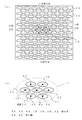
図1は本発明による反射性基板の第1の実施例を示す図、図2,図3、図4、図5は本発明を説明する図である。図1において、12は本発明による反射性基板で、該反射性基板上には多数の凹部14が設けられている。
FIG. 1 is a diagram showing a first embodiment of a reflective substrate according to the present invention, and FIGS. 2, 3, 4, and 5 are diagrams for explaining the present invention. In FIG. 1, reference numeral 12 denotes a reflective substrate according to the present invention, and a large number of
該凹部14の形状は図3(a)に示すように、18の長方形、20の角を斜めにした長方形、22の楕円、24の長方形と円の結合型と種々選び得るが、必ず長軸aと短軸bの直交2軸を有することが必要である。本実施例では長軸aを約20μm、短軸bを10μmに設定した。各形状の凹部の中心26が中心点である。なお本明細書の図面では凹部14が楕円である例を示している。凹部14は凸部に形成しても光学特性上効果はほぼ同等である。また本発明では凹部を密に配置することが可能になったので、実際の反射性基板の出来上がり形状では凹部とした時も凸部とした時も大差がない。本明細書の実施例では凹部として説明するが、本発明には凹部も凸部も含まれることは勿論である。
図3(b)は凹部14を中心点26を通る短軸上で切断した断面形状を説明する図で、樹脂膜28上に凹部14が形成されている。短軸径約10μmに対し凹部の深さは約1μmとなるよう設計されている。凹部の深さを1μmに設定した結果、凹部の斜面角度は約1
0°となっている。
図3(c)は凹部14を凸部に変えた時の形状を説明する断面図で、凸部の場合は図示のように樹脂膜28の表面に凸部29を形成すればよい。
As shown in FIG. 3 (a), the shape of the
FIG. 3B is a diagram for explaining a cross-sectional shape obtained by cutting the
It is 0 °.
FIG. 3C is a cross-sectional view for explaining the shape when the
図1に戻って、凹部14は図1(a)の点線で囲った部分16のように、図3(a)に示した各凹部の中心点26が六方細密格子の格子点に配置されている。図1(b)は点線部16の拡大図で、格子点30,32,34,36,38,40,42で六方細密格子を形成しており、7個の各凹部14の図示していない中心点26は各格子点に配置されている。格子点30と隣接する6個の格子点32,34,36,38,40,42とを各々結ぶ実線の細線で示した6本の線が中心軸で、中心軸のうち格子点30と32を結ぶ中心軸44と、格子点30と34を結ぶ中心軸46とは凹部14の長軸方向と略平行になるように配置されている。
Returning to FIG. 1, the
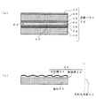
図2(a)はこのような反射性基板12を用いた液晶表示パネルの断面図で、上側の透明な基板48の上面には偏光板52、下面には上側透明電極56が設けられ下側の透明な基板50の上面には反射層54が設けられ、さらにその上部に下側透明電極58が設けられている。基板48と50はシール部60,62によってシールされ、基板48,50,シール部60,62によって出来た間隙で液晶物質が狭持されて液晶層64を構成している。これらの要素により液晶表示パネル68が構成されている。下側の透明な基板50と反射層54で図1(a)の反射性基板12が構成されているが、液晶パネルに用いられる時には液晶パネル画面に対して図1(a)の反射性基板12の上方が12時方向、下方が6時方向、右方が3時方向、左方が9時方向になるよう取り付けられる。従って図1(b)の中心軸44,46が3時9時方向と略平行になる。
FIG. 2A is a cross-sectional view of a liquid crystal display panel using such a reflective substrate 12. A polarizing plate 52 is provided on the upper surface of the upper
ここで少なくとも下側透明電極58は分割され、複数の画素を構成している。また該画素毎に反射性膜の一部を除去し、かつ液晶パネル68下面にバックライト等を置いて、透過・反射両用タイプパネルとすることは通常の技術で実現可能である。なお簡単のため、図2(a)においては配向膜等の図示を省略している。 Here, at least the lower transparent electrode 58 is divided into a plurality of pixels. Further, it is possible to realize a transmissive / reflective type panel by removing a part of the reflective film for each pixel and placing a backlight or the like on the lower surface of the liquid crystal panel 68 by a normal technique. For the sake of simplicity, the alignment film and the like are not shown in FIG.
図2(b)は本発明による反射性基板12の断面図で、下側の透明な基板50上に 、
凹部備える樹脂膜28と、該樹脂膜28上に反射膜66とを備えている。これらによって反射性基板12が構成されている。
FIG. 2 (b) is a cross-sectional view of the reflective substrate 12 according to the present invention, on the lower
A
なお本明細書を通じて、同様の部材には同様の番号を付している。 Throughout this specification, similar members are denoted by the same reference numerals.
このように反射性基板12を構成した結果、本発明によれば、各格子点上の凹部14を取り除かなくとも干渉縞が目立たなくなることが分かった。このような効果を生んだのは、凹部を長軸と短軸を有する楕円もしくは長方形もしくは両者の中間的な形状とし、かつ六方細密格子状に配置し、その中心軸のうち、少なくとも1つの中心軸が、凹部の長軸方向と略平行になるように凹部を配置した効果と思われる。
As a result of configuring the reflective substrate 12 in this manner, it has been found that according to the present invention, interference fringes become inconspicuous without removing the
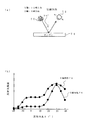
図5は本発明による反射性基板および該反射性基板を用いた液晶表示パネルの光反射特性を説明する図で、図5(a)は測定法を説明する図、図5(b)は液晶表示パネルを測定した特性図である。
図5(a)において、サンプル74は本発明の反射性基板12を用いた液晶表示パネル68である。光源70はサンプル74の法線方向から30°の角度の位置に設け、Y軸方向の特性を測定する時は12時方向30°の位置、X軸方向の特性を測定するときは9時方向30°の位置に設ける。反射光強度は輝度計72によって測定する。Y軸方向の特性を測定する時は液晶パネルの12時から6時方向に輝度計を走査して測定し、X軸方向の特性を測定する時は9時から3時方向に輝度計を走査して測定する。
5A and 5B are diagrams for explaining light reflection characteristics of a reflective substrate according to the present invention and a liquid crystal display panel using the reflective substrate. FIG. 5A is a diagram for explaining a measurement method, and FIG. It is the characteristic view which measured the display panel.
In FIG. 5A, a sample 74 is a liquid crystal display panel 68 using the reflective substrate 12 of the present invention. The light source 70 is provided at an angle of 30 ° from the normal direction of the sample 74. When measuring the characteristic in the Y axis direction, the position is 30 ° in the 12 o'clock direction, and when measuring the characteristic in the X axis direction, it is 9 o'clock. Provided at 30 ° position. The reflected light intensity is measured by the luminance meter 72. When measuring characteristics in the Y-axis direction, scan the luminance meter from 12 o'clock to 6 o'clock on the liquid crystal panel, and when measuring characteristics in the X-axis direction, scan the luminance meter from 9 o'clock to 3 o'clock. And measure.
図5(b)が本発明による反射性基板12の反射光強度特性で、縦軸が反射光強度、横軸が反射角度を示している。ここで、反射光強度は、標準白色板に対する相対反射率を示し、反射角度は、サンプルの法線方向からの角度を示し、サンプル法線に対して、光源側を負とし、光源と反対側を正とする。
76がY軸の反射光強度特性で、12時から6時方向に輝度計を走査して測定したデータ、78がX軸の反射光強度特性で、9時から3時方向に輝度計を走査して測定したデータである。X軸特性78を見るとサンプル74の法線方向から−15°くらいの所から反射光強度が立ち上がり、15°を超えた角度から急激に上昇して30°がピークとなっている。Y軸特性76を見ると、法線方向から−20°くらいの所から反射光強度が立ち上がり、−15〜−5°にかけて急激に上昇し、−5〜10°の角度ではほぼ平坦になり、15°くらいから再度上昇して30°がピークとなっている。
図5(b)から明らかなように、X軸方向とY軸方向とでは明らかに反射光量に差がある。これは凹部を楕円的な形状にし、凹部の長軸方向を3時9時の方向と平行になっている効果で、3時9時の方向と平行な斜面、つまり、12時方向からの光を法線方向に反射させることの出来る反射面が増大したためで、一方12時6時の方向と平行な斜面、つまり、9時方向からの光を法線方向に反射させることの出来る反射面は減少したためである。
この状況は、12時方向から入射された光の多くが法線方向に反射することを示している。実使用時において、液晶表示パネルを反射型で使用する時の外光は、液晶パネルの12時方向から入射することが多いため、本発明の反射性基板を用いれば、法線方向への光指向性を実現できたと考えられる。
FIG. 5B shows the reflected light intensity characteristic of the reflective substrate 12 according to the present invention, where the vertical axis represents the reflected light intensity and the horizontal axis represents the reflection angle. Here, the reflected light intensity indicates the relative reflectance with respect to the standard white plate, the reflection angle indicates the angle from the normal direction of the sample, the light source side is negative with respect to the sample normal, and the opposite side to the light source Is positive.
76 is the Y-axis reflected light intensity characteristic, data measured by scanning the luminance meter from 12 o'clock to 6 o'clock direction, 78 is the X-axis reflected light intensity characteristic, and the luminance meter is scanned from 9 o'clock to 3 o'clock direction It is the data measured. Looking at the X-axis characteristic 78, the reflected light intensity rises from about −15 ° from the normal direction of the sample 74, rapidly rises from an angle exceeding 15 °, and peaks at 30 °. Looking at the Y-axis characteristic 76, the reflected light intensity rises from about −20 ° from the normal direction, rises sharply from −15 to −5 °, and becomes substantially flat at an angle of −5 to 10 °, It rises again from around 15 ° and peaks at 30 °.
As is clear from FIG. 5B, the amount of reflected light is clearly different between the X-axis direction and the Y-axis direction. This is the effect that the concave portion is made into an elliptical shape, and the major axis direction of the concave portion is parallel to the direction of 3 o'clock to 9 o'clock. Since the number of reflective surfaces that can reflect the light in the normal direction has increased, the slope parallel to the 12 o'clock direction, that is, the reflective surface that can reflect light from the 9 o'clock direction in the normal direction is This is because it decreased.
This situation indicates that most of the light incident from the 12 o'clock direction is reflected in the normal direction. In actual use, external light when the liquid crystal display panel is used in a reflective type often enters from the 12 o'clock direction of the liquid crystal panel. Therefore, if the reflective substrate of the present invention is used, light in the normal direction is used. It seems that directivity was achieved.
このように本発明の反射性基板12によれば、「所望の角度への光指向性を持たせること」と「干渉縞の発生を押さえる事」の2点を共に満足することが出来、効果は大きい。 As described above, according to the reflective substrate 12 of the present invention, it is possible to satisfy both of the two points of “giving light directivity to a desired angle” and “suppressing generation of interference fringes”. Is big.
図9は本発明の反射性基板12の製造方法を説明する図で、凹部14を有する反射性基板の各製造工程を図示している。
FIG. 9 is a diagram for explaining a method of manufacturing the reflective substrate 12 according to the present invention, and illustrates each manufacturing process of the reflective substrate having the
図9(a)の工程ではガラス等の透明基板50上にポジ型感光性の1層目樹脂膜116を2.5μm厚程度スピンコート法で塗布している。
In the process of FIG. 9A, a positive photosensitive first-layer resin film 116 is applied on a
図9(b)の工程でマスク118を用いて図9(a)の1層目樹脂膜116を露光、現像する。マスク118の開口部120は楕円形となっており、上面から見ると楕円形の開口部122が六方細密格子の格子点に並んでいる。現像された1層目樹脂膜124は凹部となるべきところが楕円形に除去された形状となっている。 In the step of FIG. 9B, the first resin film 116 of FIG. 9A is exposed and developed using the mask 118. The opening 120 of the mask 118 has an elliptical shape, and when viewed from the top, the elliptical opening 122 is aligned with the lattice points of the hexagonal close-packed lattice. The developed first-layer resin film 124 has a shape in which a portion to be a recess is removed in an elliptical shape.
その後、1層目樹脂膜124の透明性を得るために、高圧水銀灯を光源とした露光装置を用いて紫外線を全面に照射する。さらに、クリーンオーブンにて220℃で60分の焼成を行い、1層目樹脂膜124を熱硬化する。 Thereafter, in order to obtain transparency of the first-layer resin film 124, the entire surface is irradiated with ultraviolet rays using an exposure apparatus using a high-pressure mercury lamp as a light source. Further, baking is performed at 220 ° C. for 60 minutes in a clean oven to thermally cure the first resin film 124.
図9(c)は2層目樹脂膜126を塗布する工程で、1層目樹脂膜116,124と同材質の樹脂を2μm厚程度やはりスピンコート法で塗布している。 FIG. 9C shows a step of applying a second layer resin film 126, in which a resin having the same material as that of the first layer resin films 116 and 124 is applied by a spin coating method to a thickness of about 2 μm.
その後、2層目樹脂膜126の透明性を得るために、高圧水銀灯を光源とした露光装置を用いて紫外線を全面に照射する。さらに、クリーンオーブンにて220℃で60分の焼成を行い、2層目樹脂膜126を熱硬化する。 Thereafter, in order to obtain transparency of the second-layer resin film 126, the entire surface is irradiated with ultraviolet rays using an exposure apparatus using a high-pressure mercury lamp as a light source. Further, baking is performed at 220 ° C. for 60 minutes in a clean oven to thermally cure the second layer resin film 126.
図9(d)は凹部を持った完成樹脂膜28を示した図である。完成状態で樹脂膜28の凹部のへこみは1μm程度、樹脂膜28の平均的な層厚は3.5〜4.5μm程度となっている。一層目樹脂膜116を2.5μm程度に設定すると、完成状態で1μm程度の凹
みが得られる。この段階では、凹部が非常に密に配置されているため、樹脂膜28上に平坦な部分は少なくなっている。よって連続した波状の凹凸が配置された形状となっている。
FIG. 9D is a view showing a completed
図9(e)は反射膜成膜工程で、ここではスパッタ法でアルミ合金膜66を樹脂膜28上全面に成膜している。このようにして図2(b)に示した反射性基板12が得られる。
FIG. 9E shows a reflective film forming process, in which an aluminum alloy film 66 is formed on the entire surface of the
図4は本発明をより明瞭に定義するための図で、反射性基板80上に多数の凹部14が設けられている。該凹部14は図4(a)の点線で囲った部分82のように図1と同じように各凹部の中心点26が六方細密格子の格子点に配置されている。図4(b)は点線部82の拡大図で、格子点84,86,88,90,92,94,96で六方細密格子を形成しており、7個の各凹部14の図示していない中心点26は各格子点に配置されている。図1と異なるのは六方細密格子の形状である。図4でも格子点84から見た中心軸を6本の実線の細線で示しているが、図1(b)では中心軸のうち格子点30と32を結ぶ中心軸44と、格子点30と34を結ぶ中心軸46とが凹部14の長軸方向と略平行になるように配置されていたのに対し、図4(b)では長軸方向と略平行になるような中心軸が存在せず、格子点84と92を結ぶ中心軸100と、格子点84と94を結ぶ中心軸98とが凹部14の短軸方向と略平行になるように配置されている。一方図1(b)には短軸方向と略平行な中心軸は存在しない。図4(a)のように凹部14を配置すると、特に6時12時方向から見ると規則性が強く、干渉縞が目立つことが判明した。
すなわち六方細密格子に配置すると、六方細密格子の中心格子点から周りの格子点とを結ぶ中心軸の配置と直交二軸を有する形状の凹凸の長軸方向との組み合わせとして、平行方向に設置するか、直行方向に設置するかの2パターン考えられるが、平行方向にそれぞれを設置することによって、干渉縞を目立たなくすることができることが分かった。このように六方細密格子の中心軸のうち、少なくとも1つの中心軸が、凹部の長軸方向と略平行になるような六方細密格子の各格子点に凹部を配置することが本発明の特徴で、図4のように、少なくとも1つの中心軸が凹部の短軸方向と略平行になるような六方細密格子を
採用した場合は本発明の効果は生じない。
FIG. 4 is a view for more clearly defining the present invention, and a large number of
That is, when arranged in a hexagonal close-packed lattice, it is installed in a parallel direction as a combination of the arrangement of the central axis connecting the central lattice points of the hexagonal close-packed lattice with the surrounding lattice points and the major axis direction of the concave and convex shape having two orthogonal axes. It can be considered that the patterns are arranged in the orthogonal direction, but the interference fringes can be made inconspicuous by installing each in the parallel direction. As described above, the feature of the present invention is that the recesses are arranged at the respective lattice points of the hexagonal close-packed lattice so that at least one of the center axes of the hexagonal close-packed lattice is substantially parallel to the major axis direction of the recess. As shown in FIG. 4, when a hexagonal close-packed lattice in which at least one central axis is substantially parallel to the minor axis direction of the recess is employed, the effect of the present invention does not occur.
図7は本発明による反射性基板の第2の実施例を示す図で、格子点をランダムに移動させて各格子点上に凹部を配置した例である。図7のように反射性基板102上で格子点をランダムに移動させると図1の場合よりもさらに干渉縞が目立たなくなるという効果が生じた。このような反射性基板102は図9(b)のマスク118のパターンを変えるだけで、図9と同様の方法で製造可能である。 FIG. 7 is a diagram showing a second embodiment of the reflective substrate according to the present invention, in which the lattice points are randomly moved and concave portions are arranged on the respective lattice points. When the lattice points are moved randomly on the reflective substrate 102 as shown in FIG. 7, the effect that the interference fringes become inconspicuous further than in the case of FIG. Such a reflective substrate 102 can be manufactured by the same method as in FIG. 9 only by changing the pattern of the mask 118 in FIG.
図8は本発明による反射性基板の第3の実施例を示す図で、凹部における各々の形状または大きさをランダムに変化させた例である。凹部の長軸の長さ、短軸の長さを複数種類用意した。種類は多ければそれだけ干渉縞が目立たなくなるが、図8(b)では、図8(a)に示した104,106,108,110の4種類の形状の凹部を用いて作図している。図8(b)のように反射性基板112上に各々の形状をランダムに変化させた凹部を配置すると、実施例2の場合と同様に図1の場合よりもさらに干渉縞が目立たなくなるという効果が生じた。このような反射性基板112は図9(b)のマスク118のパターンを変えるだけで、図9と同様の方法で製造可能である。 FIG. 8 is a view showing a third embodiment of the reflective substrate according to the present invention, in which each shape or size in the recess is randomly changed. A plurality of types of major axis lengths and minor axis lengths of the recesses were prepared. If there are many types, the interference fringes become inconspicuous. However, in FIG. 8B, the drawing is performed using the concave portions of four types 104, 106, 108, and 110 shown in FIG. 8A. If concave portions whose shapes are randomly changed are arranged on the reflective substrate 112 as shown in FIG. 8B, the interference fringes are less noticeable than in the case of FIG. Occurred. Such a reflective substrate 112 can be manufactured by a method similar to that shown in FIG. 9 only by changing the pattern of the mask 118 shown in FIG.
なお図8(b)の点線に囲まれた部分114に示すように、実施例3においては、凹部の中心点を図1と同様の六方細密格子の格子点上に配置している。また実施例3のように、凹部の形状もしくは大きさを変えた上、さらに実施例2のように格子点をランダムに移動しても良い結果が得られることは勿論である。 As shown in a portion 114 surrounded by a dotted line in FIG. 8B, in the third embodiment, the center point of the concave portion is arranged on a lattice point of a hexagonal close-packed lattice similar to FIG. Further, as in the third embodiment, it is a matter of course that the result may be obtained by changing the shape or size of the recesses and further moving the lattice points randomly as in the second embodiment.
このように本発明によれば、干渉縞が目立たず、かつ所望の角度で明るい画像が得られ効果は大きい。 As described above, according to the present invention, interference fringes are not conspicuous and a bright image can be obtained at a desired angle.
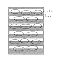
図10は本発明による反射性基板の第4の実施例を示す図で、反射膜66を凹部14の一部に形成した例である。このように、反射膜を一部取り除き、反射膜に開口部を形成することによって、反射表示だけでなく透過表示を可能とする半透過反射型の液晶表示パネルを作成することができる。このとき、凹部14の6時方向の斜面に沿って、帯状に反射膜66を配置すれば、12時方向からの光を効率よく反射することができ、反射時における液晶表示パネルの光量を増大する効果が生じる。
FIG. 10 is a view showing a fourth embodiment of the reflective substrate according to the present invention, in which a reflective film 66 is formed in a part of the
特に本発明では、凹部の中心点を六方細密格子の格子点に配置し、かつ任意の中心軸を凹部の長軸方向と平行に、そして3時9時方向と平行な方向に配置しているため、反射膜を帯状に配置すれば、それぞれの凹部の6時方向の斜面に効率よく反射膜を配置することができる。 In particular, in the present invention, the center point of the concave portion is arranged at the lattice point of the hexagonal close-packed lattice, and the arbitrary central axis is arranged in parallel with the major axis direction of the concave portion and in the direction parallel to the 3 o'clock to 9 o'clock direction. Therefore, if the reflective film is disposed in a band shape, the reflective film can be efficiently disposed on the slope of each recess at 6 o'clock.
図10で配置した帯状の反射膜を配置した反射性基板は反射特性を重視した反射膜配置であるが、透過特性を重視した反射膜配置とした例を図11に示す。図11では、図10と同様に、凹部14の6時方向の斜面に反射膜66が帯状に配置されているが、反射膜66を配置した面積を少なくし、反射膜の開口部を大きくして透過特性を重視している。このように、反射膜の配置面積を制御することによって、反射および透過の特性を制御することが可能である。
The reflective substrate on which the band-shaped reflective film arranged in FIG. 10 is arranged is a reflective film arrangement that places importance on the reflection characteristics, but FIG. 11 shows an example of a reflective film arrangement that places importance on the transmission characteristics. In FIG. 11, as in FIG. 10, the reflective film 66 is disposed in a strip shape on the slope of the
a 長軸
b 短軸
14 凹部
29 凸部
28 樹脂膜
66 反射膜
26 凹部の中心点
30,32,34,36,38,40 格子点
44,46 中心軸
12 反射性基板
68 液晶表示パネル
a major axis b
Claims (9)
前記樹脂膜上に反射膜とを基板上に備える反射性基板であって、
前記凹部または凸部の中心点は六方細密格子の格子点に配置され、
任意の前記格子点と隣接する6個の格子点とを各々結ぶ線を中心軸とし、
該中心軸のうち少なくとも1つの中心軸が、前記凹部または凸部の長軸方向と略平行になるように、
前記凹部または凸部を配置したことを特徴とする反射性基板。 A resin film provided with a concave portion or a convex portion having a shape having two orthogonal axes of a major axis and a minor axis;
A reflective substrate provided on the substrate with a reflective film on the resin film,
The center point of the concave or convex portion is arranged at a lattice point of a hexagonal close-packed lattice,
A line connecting each arbitrary lattice point and six adjacent lattice points is a central axis,
At least one central axis of the central axes is substantially parallel to the major axis direction of the concave portion or the convex portion,
The reflective board | substrate characterized by arrange | positioning the said recessed part or convex part.
前記一対の基板のうち、一方の基板は前記画素内に長軸と短軸の直交二軸を有する形状の凹部または凸部を備える樹脂膜と前記樹脂膜上に反射膜とを備える基板であり、
前記凹部または凸部の中心点は六方細密格子の格子点に配置され、
任意の前記格子点と隣接する6個の格子点とを各々結ぶ線を中心軸とし、
該中心軸のうち少なくとも1つの中心軸が、前記凹部または凸部の長軸方向と略平行になるように、
前記凹部または凸部を配置したことを特徴とする液晶表示パネル。 A liquid crystal display panel having a plurality of pixels with a liquid crystal sandwiched between a pair of substrates,
Of the pair of substrates, one substrate is a substrate provided with a resin film provided with a concave or convex portion having a shape in which the major axis and the minor axis are orthogonal to each other in the pixel, and a reflective film on the resin film. ,
The center point of the concave or convex portion is arranged at a lattice point of a hexagonal close-packed lattice,
A line connecting each arbitrary lattice point and six adjacent lattice points is a central axis,
At least one central axis of the central axes is substantially parallel to the major axis direction of the concave portion or the convex portion,
A liquid crystal display panel comprising the concave portion or the convex portion.
Priority Applications (1)
| Application Number | Priority Date | Filing Date | Title |
|---|---|---|---|
| JP2004160400A JP2005099705A (en) | 2003-09-03 | 2004-05-31 | Reflective substrate and liquid crystal display panel using the same |
Applications Claiming Priority (2)
| Application Number | Priority Date | Filing Date | Title |
|---|---|---|---|
| JP2003310980 | 2003-09-03 | ||
| JP2004160400A JP2005099705A (en) | 2003-09-03 | 2004-05-31 | Reflective substrate and liquid crystal display panel using the same |
Publications (2)
| Publication Number | Publication Date |
|---|---|
| JP2005099705A true JP2005099705A (en) | 2005-04-14 |
| JP2005099705A5 JP2005099705A5 (en) | 2007-03-22 |
Family
ID=34467546
Family Applications (1)
| Application Number | Title | Priority Date | Filing Date |
|---|---|---|---|
| JP2004160400A Pending JP2005099705A (en) | 2003-09-03 | 2004-05-31 | Reflective substrate and liquid crystal display panel using the same |
Country Status (1)
| Country | Link |
|---|---|
| JP (1) | JP2005099705A (en) |
Citations (3)
| Publication number | Priority date | Publication date | Assignee | Title |
|---|---|---|---|---|
| JPS55103583A (en) * | 1979-01-31 | 1980-08-07 | Nippon Electric Co | Reflecting transmission body |
| JPS58192075A (en) * | 1982-05-06 | 1983-11-09 | セイコーエプソン株式会社 | Liquid crystal panel |
| JP2002258270A (en) * | 2000-12-25 | 2002-09-11 | Seiko Epson Corp | Substrate for liquid crystal device, its manufacturing method, liquid crystal device, its manufacturing method and electronic equipment |
-
2004
- 2004-05-31 JP JP2004160400A patent/JP2005099705A/en active Pending
Patent Citations (3)
| Publication number | Priority date | Publication date | Assignee | Title |
|---|---|---|---|---|
| JPS55103583A (en) * | 1979-01-31 | 1980-08-07 | Nippon Electric Co | Reflecting transmission body |
| JPS58192075A (en) * | 1982-05-06 | 1983-11-09 | セイコーエプソン株式会社 | Liquid crystal panel |
| JP2002258270A (en) * | 2000-12-25 | 2002-09-11 | Seiko Epson Corp | Substrate for liquid crystal device, its manufacturing method, liquid crystal device, its manufacturing method and electronic equipment |
Similar Documents
| Publication | Publication Date | Title |
|---|---|---|
| KR100386856B1 (en) | Liquid crystal display device | |
| US7944544B2 (en) | Liquid crystal device having a diffraction function layer that includes a flat portion and a non-flat portion with a grid disposed in the non-flat portion | |
| CN101526685B (en) | Color film substrate and manufacture method thereof | |
| US6995898B2 (en) | Mask, substrate with light reflecting film, method for forming light reflecting film, method for manufacturing electro-optical device, electro-optical device, and electronic apparatus | |
| US20070111115A1 (en) | Light reflective structure, method for producing the same and display | |
| JP2002139630A (en) | Light transmission plate, method for manufacturing the same, surface light-emitting device and liquid crystal display | |
| JP2006309002A (en) | Optical film without moire fringe, applied to backlight for liquid crystal display device | |
| JP2005300907A (en) | Screen and image projection system using the same | |
| JP3974787B2 (en) | Reflective liquid crystal display | |
| JPH11326615A (en) | Reflecting plate and reflection type liquid crystal display device | |
| JP4655414B2 (en) | Anti-glare optical film | |
| JP4967689B2 (en) | Exposure method, exposure apparatus, and method of manufacturing color filter for transflective liquid crystal display device | |
| TWI250330B (en) | Manufacturing method of electro-optical device substrate and manufacturing method of electro-optical device | |
| JP2005099705A (en) | Reflective substrate and liquid crystal display panel using the same | |
| TWI254147B (en) | Reflector for liquid crystal display | |
| JP2002090512A (en) | Reflector and reflection type liquid crystal display device having the reflector | |
| JP4028290B2 (en) | Liquid crystal display device and manufacturing method thereof | |
| KR100660671B1 (en) | Electro-optic device substrate and method for manufacturing the same, electro-optic device and method for manufacturing the same, photomask, and electronic device | |
| JP2004294506A (en) | Liquid crystal display with fresnel lens reflection layer | |
| JP2004199050A (en) | Reflective substrate and liquid crystal display panel using the same | |
| JP2005055829A (en) | Method for manufacturing transflective film | |
| JP2005018008A (en) | Translucent type collar liquid crystal display element and reflective type collar liquid crystal display element, and manufacturing method therefor | |
| JP2003043478A (en) | Liquid crystal display device | |
| JP2003131216A (en) | Liquid crystal display panel | |
| JP4880839B2 (en) | Method for manufacturing transflective liquid crystal display element |
Legal Events
| Date | Code | Title | Description |
|---|---|---|---|
| A521 | Written amendment |
Free format text: JAPANESE INTERMEDIATE CODE: A523 Effective date: 20070205 |
|
| A621 | Written request for application examination |
Free format text: JAPANESE INTERMEDIATE CODE: A621 Effective date: 20070205 |
|
| A977 | Report on retrieval |
Free format text: JAPANESE INTERMEDIATE CODE: A971007 Effective date: 20091027 |
|
| A131 | Notification of reasons for refusal |
Free format text: JAPANESE INTERMEDIATE CODE: A131 Effective date: 20100105 |
|
| A02 | Decision of refusal |
Free format text: JAPANESE INTERMEDIATE CODE: A02 Effective date: 20100713 |