JP2005057655A - Imaging apparatus - Google Patents
Imaging apparatus Download PDFInfo
- Publication number
- JP2005057655A JP2005057655A JP2003288865A JP2003288865A JP2005057655A JP 2005057655 A JP2005057655 A JP 2005057655A JP 2003288865 A JP2003288865 A JP 2003288865A JP 2003288865 A JP2003288865 A JP 2003288865A JP 2005057655 A JP2005057655 A JP 2005057655A
- Authority
- JP
- Japan
- Prior art keywords
- gain
- amplifying
- imaging apparatus
- imaging
- amplifying means
- Prior art date
- Legal status (The legal status is an assumption and is not a legal conclusion. Google has not performed a legal analysis and makes no representation as to the accuracy of the status listed.)
- Pending
Links
Images


Classifications
-
- H—ELECTRICITY
- H04—ELECTRIC COMMUNICATION TECHNIQUE
- H04N—PICTORIAL COMMUNICATION, e.g. TELEVISION
- H04N25/00—Circuitry of solid-state image sensors [SSIS]; Control thereof
- H04N25/60—Noise processing, e.g. detecting, correcting, reducing or removing noise
- H04N25/67—Noise processing, e.g. detecting, correcting, reducing or removing noise applied to fixed-pattern noise, e.g. non-uniformity of response
- H04N25/671—Noise processing, e.g. detecting, correcting, reducing or removing noise applied to fixed-pattern noise, e.g. non-uniformity of response for non-uniformity detection or correction
- H04N25/672—Noise processing, e.g. detecting, correcting, reducing or removing noise applied to fixed-pattern noise, e.g. non-uniformity of response for non-uniformity detection or correction between adjacent sensors or output registers for reading a single image
Abstract
Description
本発明は、複数の出力端子を有する撮像素子を用いた撮像装置に関する。 The present invention relates to an imaging apparatus using an imaging device having a plurality of output terminals.
近年ディジタル信号処理技術及び半導体技術の進歩により、標準テレビ方式、例えばNTSC方式やPAL方式の動画像信号をディジタル記録する民生用ディジタルビデオ規格が提案されており、その応用として、ディジタルビデオ記録再生装置と撮像装置を一体化したディジタルビデオカメラが製品化されている。このようなディジタルビデオカメラでは、ディジタル記録という特徴を生かして、静止画記録機能を備えるものがある。また、コンピュータ等との接続のためにディジタルI/Fを具備し、撮影した画像をコンピュータに取り込む機能を有するものもある。さらに、複数の記録媒体を具備し、画像の使用目的に応じて記録媒体を選択できるようになっているものもある。 In recent years, with the advancement of digital signal processing technology and semiconductor technology, consumer digital video standards for digitally recording standard television system, for example, NTSC system and PAL system video signals, have been proposed. A digital video camera that integrates an image pickup device has been commercialized. Some digital video cameras have a still image recording function by taking advantage of the feature of digital recording. Some have a digital I / F for connection to a computer or the like, and have a function of taking a captured image into the computer. Furthermore, there are some which have a plurality of recording media and can select the recording media according to the purpose of use of the image.
このような装置において、記録された画像をテレビに接続して再生する場合は、その画像サイズはディジタルビデオ規格で定められるもの、例えば720x480画素でなんら問題は無いが、ディジタルI/Fを介して他のメディアに画像を転送する場合は、画質上の問題からより多くの画素数が要求される場合がある。 In such an apparatus, when a recorded image is played back by connecting it to a television, the image size is determined by the digital video standard, for example, 720 × 480 pixels, there is no problem, but via a digital I / F. When transferring an image to other media, a larger number of pixels may be required due to image quality problems.
撮像素子の多画素化に伴い、撮像素子の全画素の情報を読み出すためにはより高い周波数で撮像素子を駆動する必要があり、S/Nの劣化や消費電力の増大を招く。 Accompanying the increase in the number of pixels of the image sensor, it is necessary to drive the image sensor at a higher frequency in order to read out information of all the pixels of the image sensor, leading to S / N degradation and increased power consumption.
撮像素子の駆動周波数を低く抑えたまま撮像情報のデータレートを上げる方法の一つとして、撮像面を複数の領域に分割し、それぞれの領域に独立した電荷転送部、増幅器及び出力端子を持たせ、撮像信号を並列に読み出す方法がある。このような撮像素子を用いた撮像装置の例を図8に示す。同図において撮像素子800の撮像面は左右の2領域に分割されており、801、802は光電変換及び垂直転送部、803、804は水平転送部、805、806は増幅器、807、808は出力端子である。このような構造の撮像素子を用いることにより、撮像素子の駆動周波数に対し2倍のデータレートの撮像情報が得られる利点がある。
As one method for increasing the data rate of imaging information while keeping the driving frequency of the imaging device low, the imaging surface is divided into a plurality of regions, and independent charge transfer units, amplifiers, and output terminals are provided in each region. There is a method of reading the imaging signals in parallel. An example of an imaging apparatus using such an imaging element is shown in FIG. In the figure, the imaging surface of the
不図示の結像光学系により撮像素子800上に結像した被写体像は撮像素子800により電気信号に変換され、不図示の駆動タイミング発生回路から供給される駆動パルスに応じて出力端子807,808より出力される。
A subject image formed on the
撮像素子800から得られる2系統の画像信号は809、810によりアナログ信号処理を施された後AD変換され、増幅器813、814で所定のレベルに増幅された後、画面合成回路817にて左右の画像が一枚の画像として合成された後、カメラ信号処理回路818にてγ補正処理、輪郭補正処理、色補正処理などを施され、輝度信号及び色差信号として出力端子819より出力される(例えば、特許文献1)。
しかしながら上記従来例では、各領域の増幅器及び外部周辺回路の特性の不均一性により、2つの領域を合成して画像を生成した場合に、領域間のレベル差による境界線が生じるなどの画質劣化が発生する問題があった。 However, in the above conventional example, due to the non-uniformity of the characteristics of the amplifier and external peripheral circuit in each region, image quality deterioration such as a boundary line due to a level difference between the regions occurs when two regions are combined to generate an image. There was a problem that occurred.
上記課題を解決するために、少なくとも第1、第2の出力端子を持つ撮像素子を用いた撮像装置であって、前記撮像素子の複数の出力信号に対してそれぞれ独立に信号を増幅する第1、第2の増幅手段と、前記第1、第2の増幅手段に与える利得を制御する利得制御手段と、前記第1の増幅手段の利得に対応した前記第2の増幅手段のゲインテーブルと、を備え、前記利得制御手段は前記第1の増幅手段の利得を制御するとともにゲインテーブルから前記第2の増幅手段の利得に対応した利得を用いて前記第2の増幅手段を制御することを特徴とする撮像装置を提供する。 In order to solve the above-described problem, an image pickup apparatus using an image pickup device having at least first and second output terminals, the first device amplifying signals independently of a plurality of output signals of the image pickup device. A second amplifying means; a gain control means for controlling the gain applied to the first and second amplifying means; a gain table of the second amplifying means corresponding to the gain of the first amplifying means; The gain control means controls the gain of the first amplifying means and controls the second amplifying means using a gain corresponding to the gain of the second amplifying means from a gain table. An imaging apparatus is provided.
映像信号を増幅する際の利得に応じてゲインテーブルから別のチャンネルの利得を制御することが出来るので、利得が変化した場合でも撮像素子からの複数の出力信号の差分による境界を目立たなくし、段差を無くすことが出来る。 Since the gain of another channel can be controlled from the gain table according to the gain when amplifying the video signal, even if the gain changes, the boundary due to the difference between the multiple output signals from the image sensor becomes inconspicuous, and the level difference Can be eliminated.
(実施の形態1)
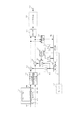
図1は、単板ビデオカメラにおける本発明の第1の実施形態を概略的に示す図である。同図において、100は撮像領域が2分割され、それぞれに出力端子を持つCCDエリアセンサ、101、102は光電変換部及び垂直転送部、103、104は水平転送部であり画面の中心を境に左右方向に2分割されている。105、106は信号電荷を増幅する出力アンプ、107、108は撮像信号の出力端子である。109、110は相関2重サンプルとAD変換を行うアナログフロントエンド、113、114はゲインを調整するゲイン調整回路、115は利得制御回路、112は対数値をリニアに変換するdB/リニア変換回路、116は2系統間の不均一性を検出するための段差評価値生成回路、117は2系統の画像信号を合成して1枚の画像を生成する画面合成回路、118はカメラ信号処理回路、119は出力端子、121は段差評価値からゲインテーブルを作成する調整回路、120は書き換え可能な不揮発性メモリで構成されるメモリテーブル、111はメモリテーブル120から利得データを取得してゲイン調整回路114に供給するテーブル参照回路である。
(Embodiment 1)
FIG. 1 is a diagram schematically showing a first embodiment of the present invention in a single-panel video camera. In the figure, 100 is a CCD area sensor having an imaging area divided into two and each has an output terminal, 101 and 102 are photoelectric conversion units and vertical transfer units, and 103 and 104 are horizontal transfer units, with the center of the screen as the boundary. It is divided into two in the left-right direction.
次に、上記構成における本発明の実施例の動作について説明する。 Next, the operation of the embodiment of the present invention having the above configuration will be described.
CCD100上に結像した被写体像は、光電変換部101、102により電気信号に変換された後、水平転送路103、104により2系統に分割されて出力アンプ105、106に供給される。信号電荷は出力アンプで増幅され、出力端子107、108より出力される。出力端子107から得られる撮像信号を左チャンネル信号、出力端子108から得られる撮像信号を右チャンネル信号と呼称することにする。
The subject image formed on the
左右2系統の撮像信号はアナログフロントエンド109、110により相関二重サンプル処理及びAD変換された後、ゲイン調整回路113、114に供給される。 The left and right two-line imaging signals are subjected to correlated double sample processing and AD conversion by the analog front ends 109 and 110, and then supplied to the gain adjustment circuits 113 and 114.
ゲイン調整回路113、114では、ゲイン調整が施される。ゲイン調整時に適用されるゲインは利得制御回路115より供給される。利得制御回路115は露出制御の便宜上対数値で利得を出力する為、dB/リニア変換回路112でリニア値に変換された後ゲイン調整回路113に供給される。従来の撮像装置では、低照度環境下での信号量のゲインアップをアナログ回路によって行っていたが、本実施例のように2系統の撮像信号を取り扱う撮像装置では、アナログ回路によるゲイン調整は2系統間の不均一性の要因となりうる。よって、本実施例ではゲインの調整はゲイン調整回路113,114を用いてディジタル演算により行う事で、回路のばらつきや経時変動、温度変動の影響を排除している。
The gain adjustment circuits 113 and 114 perform gain adjustment. The gain applied at the time of gain adjustment is supplied from the gain control circuit 115. The gain control circuit 115 outputs the gain as a logarithmic value for the convenience of exposure control, and is converted to a linear value by the dB /
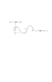
また、画像の明るさのためのゲイン調整だけでなく、2系統間のゲイン誤差の補正もここで行う。2系統間のゲインの差は一般にCCDエリアセンサ100の出力レベルの大きさに依存する。図3は2系統間のゲインの差の一例を示したものである。図の横軸はCCD100の左チャンネル出力レベルであり、縦軸はゲイン調整回路113の入力信号(左チャンネル)とゲイン調整回路114の入力信号(右チャンネル)の信号の比、すなわち2系統間の信号レベルのゲイン差を表している。例えば、ある明るさの被写体を撮像したときのCCD100の左チャンネル出力レベルをL0left、右チャンネル出力レベルをL0rightとすると、L0left、L0rightは段差評価値生成回路116で測定され、このときのゲイン差E0は次式で与えられる。
E0=L0right/L0left
この図で示されるように、信号レベルとゲイン差の関係が一定ではないので、ゲインの補正量は固定値ではなく、ゲインアップ量に応じて補正量を可変する必要がある。撮像系のゲイン制御を行う為には、片方のチャンネルに対するゲインを決定し、それに対応した他方のチャンネルのゲインを与えることが必要となる。本実施例では、左チャンネルのゲインAnleftを利得制御回路115から与え、それに対応する右チャンネルのゲインAnrightをテーブル参照回路111から与える構成になっている。
Further, not only gain adjustment for image brightness but also correction of gain error between the two systems is performed here. The gain difference between the two systems generally depends on the output level of the
E0 = L0right / L0left
As shown in this figure, since the relationship between the signal level and the gain difference is not constant, the gain correction amount is not a fixed value, and it is necessary to vary the correction amount according to the gain increase amount. In order to perform gain control of the imaging system, it is necessary to determine the gain for one channel and give the gain of the other channel corresponding to it. In this embodiment, the left channel gain Anleft is given from the gain control circuit 115, and the corresponding right channel gain Anright is given from the table reference circuit 111.
左チャンネルのゲインがA0leftの場合、右チャンネルのゲインA0rightは次式であらわされる。
A0right=E0×A0left
同様に、別のゲインAnleftの場合にはAnrightは次式であらわされる。
Anright=En×Anleft
このようにして段階的にAnleftを変化させながらEn(=Lnright/Lnleft)を測定することにより、各ゲインに対応したAnrightを求めることが出来る。
When the left channel gain is A0left, the right channel gain A0right is expressed by the following equation.
A0right = E0 × A0left
Similarly, for another gain Anleft, Anright is expressed by the following equation.
Anriight = En × Anleft
In this way, by measuring En (= Lnright / Lnleft) while changing Anleft stepwise, it is possible to obtain the Anright corresponding to each gain.
次に、ゲイン補正特性の測定について述べる。 Next, measurement of gain correction characteristics will be described.
段差評価値生成回路116は分割領域の境界付近に指定した矩形領域内の画素値を元に画面段差の評価値を算出し調整制御回路121に出力する。画面内の矩形領域の例を第2図に示す。同図に示すように2分割された領域201、202の境界近傍に、矩形領域203、204が設定され、この領域内の画素値が画面段差の評価に用いられる。CCD100は、単板でカラー画像を撮像するために、画素部にオンチップカラーフィルタが貼られている。オンチップカラーフィルタは例えば図2の205に示すようなRGBの配列である。段差評価値生成回路116では、このうちの例えばG信号などの一色の画素値を選択して領域内で平均値が計算され、これが画面段差の評価値となる。
The step evaluation value generation circuit 116 calculates the evaluation value of the screen step based on the pixel value in the rectangular area designated near the boundary of the divided area and outputs it to the adjustment control circuit 121. An example of a rectangular area in the screen is shown in FIG. As shown in the figure,
ゲイン補正特性の測定時は、明るさが一様な被写体を撮像し、利得制御回路115よりゲイン調整回路113及び114に同一のゲイン乗数を設定して行う。矩形領域203内の画素の平均レベルが左チャンネルのレベル、矩形領域204内の画素の平均レベルが右チャンネルのレベルとして、調整制御回路121に出力される。
The gain correction characteristic is measured by imaging a subject with uniform brightness and setting the same gain multiplier in the gain adjustment circuits 113 and 114 from the gain control circuit 115. The average level of the pixels in the
調整制御回路121では、左チャンネルのレベルを基準に右チャンネルのゲイン補正量を前述のように算出する。このような測定を、CCD100の出力レベルにおいて所定の間隔で行うことにより、ゲイン補正特性を生成する。調整制御回路121は、生成されたゲイン補正特性をEEPROM(Electrically Erasable Programmable Read Only Memory)などの書き換え可能な不揮発メモリで構成されたメモリテーブル120に格納する。ゲイン補正特性の生成は、例えば工場調整時などに実行される。
The adjustment control circuit 121 calculates the right channel gain correction amount as described above with reference to the level of the left channel. Such a measurement is performed at a predetermined interval at the output level of the
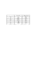
このようにして測定したゲインの表を図4に示す。図中のAnleftは対数(dB)単位の表記、Anrightはリニアの表記で、Anrightの数値は1024が1倍、2048が2倍を表す。Anleftの数値の間隔は0.264dBとしており、この間隔でのAnrightの数値をゲインテーブルとして記憶することになる。図4は左右のチャンネル間の差が全く無い状態の数値であり、実際にチャンネル間にゲイン差がある場合にはAnrightの数値が変動するものである。 A table of gains thus measured is shown in FIG. In the figure, “Anleft” is expressed in logarithmic (dB) units, “Anight” is expressed in linear, and the numerical value of “Anight” is 1024 for 1 time and 2048 for 2 times. The interval of the numerical value of Anleft is 0.264 dB, and the numerical value of Anight at this interval is stored as a gain table. FIG. 4 is a numerical value in a state where there is no difference between the left and right channels. When there is actually a gain difference between the channels, the numerical value of “Anright” fluctuates.
図5は利得制御回路およびテーブル参照回路における演算処理を示すフローチャートである。図中5−Aは利得制御回路およびdB/リニア変換回路によるAnleftのゲイン制御、5−Bはテーブル参照回路によるAnrightのゲイン制御をそれぞれ示す。撮像装置の露出を制御するブロックからゲインデータを取得すると、それぞれAnleft、Anrightに相当するゲインを左右のアンプ、即ちゲイン調整回路113、114に供給する構成である。5−Aではゲイン取得501で露出制御部から与えられる対数値のゲインデータを取得すると、dB/リニア変換502でリニアデータに変換され、Anleftとして左側のゲインアンプに出力される。一方、5−Bではゲイン取得505で露出制御部から与えられる対数値のゲインデータを取得すると、506でテーブル上のどのデータを用いるかが算出され、507でテーブルデータ510から対応したデータを取得する。ゲイン取得505で取得されたゲインがテーブルの構成データの間に位置する場合は、その前後のテーブルデータを参照し、508で補完してゲインデータを算出する。テーブルデータは対数値ではなくリニアな値なので、このままAnrightとして右側のゲインアンプに出力される。このようにして、左右のチャンネルに対して適した利得をかけることによって、等しいレベルの映像信号を得ることが出来る。
FIG. 5 is a flowchart showing arithmetic processing in the gain control circuit and the table reference circuit. In the figure, 5-A represents the gain control of the Left by the gain control circuit and the dB / linear conversion circuit, and 5-B represents the gain control of the Night by the table reference circuit. When gain data is acquired from a block that controls the exposure of the imaging apparatus, gains corresponding to Anleft and Anright are supplied to the left and right amplifiers, that is, the gain adjustment circuits 113 and 114, respectively. In 5-A, when gain data of logarithmic value given from the exposure control unit is acquired by
図中の数値はあくまでも一例であり、このままの数値でなくとも良いし、実施例は露出制御部において利得を決定する構成で説明したが、使用者が設定する構成でも構わない。 The numerical values in the figure are merely examples, and the numerical values may not be as they are. The embodiment has been described with the configuration in which the gain is determined in the exposure control unit, but the configuration may be set by the user.
(第2の実施形態)
図6は第2の実施形態の構成を示す図であり、図中の600から621は第1の実施例を示す図1の100から121と同様であり、撮像面を複数の領域に分割し、それぞれの領域に独立した電荷転送部、増幅器及び出力端子を持たせ、撮像信号を並列に読み出す撮像素子を用いた撮像装置で、各部の動作は従来例と同様である。図中、631は高温度時のテーブルデータ、630は2種類のテーブルデータから温度に応じた補正を行う温度補正回路、632は温度センサである。
(Second Embodiment)
FIG. 6 is a diagram showing the configuration of the second embodiment. Reference numerals 600 to 621 in the drawing are the same as 100 to 121 in FIG. 1 showing the first embodiment, and the imaging surface is divided into a plurality of regions. The image pickup apparatus uses an image pickup device that has an independent charge transfer unit, an amplifier, and an output terminal in each region and reads out image pickup signals in parallel. The operation of each unit is the same as that of the conventional example. In the figure, 631 is table data at a high temperature, 630 is a temperature correction circuit that performs correction according to temperature from two types of table data, and 632 is a temperature sensor.
前述した本発明の第1の実施形態で述べたように、一般に、CCDエリアセンサからAD変換に至るまでの系の各領域の増幅器及び外部周辺回路の特性の不均一性により、2つの領域を合成して画像を生成した場合に、領域間のレベル差による境界線が生じるなどの画質劣化が発生する問題があった。この特性は温度変化に応じて変化する場合があり、本発明の第1の実施例で述べた構成にしても温度変化によって領域間のレベル差による境界線が生じるなどの画質劣化が発生する。本発明の第2の実施例では、この点に鑑みて温度センサを用いて撮像素子近傍の温度に応じた補正を行うように構成されたものである。 As described in the first embodiment of the present invention described above, in general, the two areas are divided by the non-uniformity of the characteristics of the amplifier and external peripheral circuit in each area of the system from the CCD area sensor to the AD conversion. When an image is generated by synthesis, there is a problem that image quality deterioration occurs such as a boundary line due to a level difference between regions. This characteristic may change according to a temperature change. Even in the configuration described in the first embodiment of the present invention, image quality deterioration such as a boundary line due to a level difference between regions occurs due to the temperature change. In view of this point, the second embodiment of the present invention is configured to perform correction according to the temperature in the vicinity of the image sensor using a temperature sensor.
本発明の第1の実施形態で示したように工場調整時にデータテーブルを生成するが、この作業を比較的低温度の状態でおこなった低温テーブル620と、比較的高温度の状態でおこなった高温テーブル631の2種類のデータテーブルを持つ構成とする。このテーブルの例を図7に示す。図6中の温度センサ632は撮像素子近傍の温度を測定し、その情報を温度補正回路630に供給する。温度補正回路630では2種類のデータテーブルの数値からそのときの温度に適したゲインデータを算出し、テーブル参照回路611に供給する。テーブル参照回路611は本発明の第1の実施例と同様にゲインデータを算出し、右チャンネルのゲインとして与える。 As shown in the first embodiment of the present invention, a data table is generated at the time of factory adjustment, and a low temperature table 620 in which this operation is performed at a relatively low temperature and a high temperature in which the operation is performed at a relatively high temperature. The table 631 has two types of data tables. An example of this table is shown in FIG. A temperature sensor 632 in FIG. 6 measures the temperature in the vicinity of the image sensor and supplies the information to the temperature correction circuit 630. The temperature correction circuit 630 calculates gain data suitable for the temperature at that time from the values of the two types of data tables and supplies the gain data to the table reference circuit 611. The table reference circuit 611 calculates gain data in the same manner as in the first embodiment of the present invention, and provides it as the right channel gain.
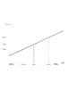
図9は温度センサ632で検出した温度から、ゲインデータを算出する手法を説明するグラフである。Temp−aは低温調整時の温度、Temp−bは高温調整時の温度、Temp−cは現在の温度、Gain−Aは低温調整時のゲイン、Gain−Bは高温調整時のゲイン、Gain−Cは算出された現在のゲインである。2種類のテーブルデータから参照された各温度に対応するGain−A、Gain−BはそれぞれTemp−a、Temp−bに対応し、現在の温度がTemp−cの場合、制御に用いるゲインはグラフからGain−Cとして算出される。 FIG. 9 is a graph illustrating a method for calculating gain data from the temperature detected by the temperature sensor 632. Temp-a is the temperature at the low temperature adjustment, Temp-b is the temperature at the high temperature adjustment, Temp-c is the current temperature, Gain-A is the gain at the low temperature adjustment, Gain-B is the gain at the high temperature adjustment, Gain- C is the calculated current gain. Gain-A and Gain-B corresponding to each temperature referenced from the two types of table data correspond to Temp-a and Temp-b, respectively, and when the current temperature is Temp-c, the gain used for control is a graph. Is calculated as Gain-C.
このようにして温度補正を加えることによって、どのような温度条件下においても撮像素子からの複数の出力信号の差分による境界を目立たなくし、段差を無くすことが出来る。 By applying the temperature correction in this way, the boundary due to the difference between the plurality of output signals from the image sensor can be made inconspicuous under any temperature condition, and the step can be eliminated.
図9中の温度補正は直線補間で説明したがその他の補間カーブを用いても構わないし、図6中のデータテーブルは2種類としたが何種類あっても構わない。また、温度センサは撮像素子近傍としたが、構成上どのような位置にあっても構わないし、このセンサを他の用途に兼用しても構わないことは言うまでも無い。 Although the temperature correction in FIG. 9 has been described by linear interpolation, other interpolation curves may be used, and there are two types of data tables in FIG. In addition, although the temperature sensor is in the vicinity of the image sensor, it may be in any position in terms of configuration, and it goes without saying that this sensor may be used for other purposes.
100 2分割読み出しCCDエリアセンサ
109、110 アナログフロントエンド
111 テーブル参照回路
112 dB/リニア変換回路
113、114 ゲインアンプ
115 利得制御回路
116 段差評価値生成回路
117 画面合成
118 カメラ信号処理
120 メモリテーブル
121 調整制御回路
100 CCD area sensor 109, 110 Analog front end 111
Claims (10)
前記撮像素子の複数の出力信号に対してそれぞれ独立に信号を増幅する第1、第2の増幅手段と、前記第1、第2の増幅手段に与える利得を制御する利得制御手段と、
前記第1の増幅手段の利得に対応した前記第2の増幅手段のゲインテーブルと、
を備え、前記利得制御手段は前記第1の増幅手段の利得を制御するとともにゲインテーブルから前記第2の増幅手段の利得に対応した利得を用いて前記第2の増幅手段を制御することを特徴とする撮像装置。 An imaging apparatus using an imaging device having at least first and second output terminals,
First and second amplifying means for independently amplifying signals with respect to a plurality of output signals of the image sensor; and gain control means for controlling gains applied to the first and second amplifying means;
A gain table of the second amplifying means corresponding to the gain of the first amplifying means;
The gain control means controls the gain of the first amplifying means and controls the second amplifying means using a gain corresponding to the gain of the second amplifying means from a gain table. An imaging device.
Priority Applications (2)
| Application Number | Priority Date | Filing Date | Title |
|---|---|---|---|
| JP2003288865A JP2005057655A (en) | 2003-08-07 | 2003-08-07 | Imaging apparatus |
| US10/913,852 US7362358B2 (en) | 2003-08-07 | 2004-08-06 | Correction of level difference between signals output from split read-out type image sensing apparatus |
Applications Claiming Priority (1)
| Application Number | Priority Date | Filing Date | Title |
|---|---|---|---|
| JP2003288865A JP2005057655A (en) | 2003-08-07 | 2003-08-07 | Imaging apparatus |
Publications (2)
| Publication Number | Publication Date |
|---|---|
| JP2005057655A true JP2005057655A (en) | 2005-03-03 |
| JP2005057655A5 JP2005057655A5 (en) | 2007-01-11 |
Family
ID=34114059
Family Applications (1)
| Application Number | Title | Priority Date | Filing Date |
|---|---|---|---|
| JP2003288865A Pending JP2005057655A (en) | 2003-08-07 | 2003-08-07 | Imaging apparatus |
Country Status (2)
| Country | Link |
|---|---|
| US (1) | US7362358B2 (en) |
| JP (1) | JP2005057655A (en) |
Cited By (4)
| Publication number | Priority date | Publication date | Assignee | Title |
|---|---|---|---|---|
| JP2007235856A (en) * | 2006-03-03 | 2007-09-13 | Fujifilm Corp | Solid imaging device |
| JP2007274212A (en) * | 2006-03-30 | 2007-10-18 | Canon Inc | Image pickup device and its control method |
| JP2009017350A (en) * | 2007-07-06 | 2009-01-22 | Hitachi Kokusai Electric Inc | Imaging device |
| JP2015087147A (en) * | 2013-10-29 | 2015-05-07 | Ckd株式会社 | Inspection apparatus and ptp packaging machine |
Families Citing this family (9)
| Publication number | Priority date | Publication date | Assignee | Title |
|---|---|---|---|---|
| JP4180076B2 (en) * | 2004-09-29 | 2008-11-12 | 三洋電機株式会社 | Signal processing device |
| JP2006157882A (en) * | 2004-10-28 | 2006-06-15 | Fuji Photo Film Co Ltd | Solid state imaging device |
| JP4763469B2 (en) * | 2005-03-07 | 2011-08-31 | 富士フイルム株式会社 | Solid-state imaging device, image input device, and image correction method thereof |
| JP4468276B2 (en) * | 2005-09-30 | 2010-05-26 | 富士フイルム株式会社 | Digital camera |
| KR100849846B1 (en) * | 2006-09-21 | 2008-08-01 | 삼성전자주식회사 | Apparatus and method for compensating brightness of image |
| US8334847B2 (en) * | 2007-10-19 | 2012-12-18 | Qnx Software Systems Limited | System having user interface using object selection and gestures |
| US8497842B2 (en) * | 2007-11-02 | 2013-07-30 | Qnx Software Systems Limited | System having user interface using motion based object selection and mouse movement |
| US8773451B2 (en) * | 2011-05-03 | 2014-07-08 | Apple Inc. | Color correction method and apparatus for displays |
| DE102018115991B4 (en) | 2018-07-02 | 2023-12-07 | Basler Ag | DIGITAL CIRCUIT FOR CORRECTING A VIGNETTING EFFECT IN PIXEL VALUES OF AN ELECTRONIC CAMERA IMAGE |
Family Cites Families (11)
| Publication number | Priority date | Publication date | Assignee | Title |
|---|---|---|---|---|
| JP3008578B2 (en) | 1991-07-10 | 2000-02-14 | ソニー株式会社 | Solid-state imaging device |
| US6072603A (en) * | 1996-02-26 | 2000-06-06 | Eastman Kodak Company | Multiple output CCD image block balancing |
| US6337713B1 (en) * | 1997-04-04 | 2002-01-08 | Asahi Kogaku Kogyo Kabushiki Kaisha | Processor for image-pixel signals derived from divided sections of image-sensing area of solid-type image sensor |
| JPH11308532A (en) | 1998-04-17 | 1999-11-05 | Nec Corp | Multi-element sensor |
| JP2002142158A (en) | 2000-11-01 | 2002-05-17 | Canon Inc | Image pickup device and correction method |
| JP3554267B2 (en) | 2000-10-12 | 2004-08-18 | キヤノン株式会社 | Imaging device, control method therefor, and signal processing method |
| EP1198127A1 (en) * | 2000-10-12 | 2002-04-17 | Canon Kabushiki Kaisha | Signal difference correction of picture signals read from multiple readout type image sensing device |
| JP3948218B2 (en) | 2001-04-19 | 2007-07-25 | ソニー株式会社 | Solid-state imaging device and driving method thereof |
| JP2003101860A (en) * | 2001-09-21 | 2003-04-04 | Canon Inc | Image pickup device, photographing image generation method, program and storage medium |
| US7218351B2 (en) * | 2002-04-05 | 2007-05-15 | Victor Company Of Japan, Limited | Image-sensing apparatus for compensating video signal of a plurality of channels |
| US7236199B2 (en) * | 2003-07-07 | 2007-06-26 | Toshikazu Hori | Multi-tap camera |
-
2003
- 2003-08-07 JP JP2003288865A patent/JP2005057655A/en active Pending
-
2004
- 2004-08-06 US US10/913,852 patent/US7362358B2/en not_active Expired - Fee Related
Cited By (5)
| Publication number | Priority date | Publication date | Assignee | Title |
|---|---|---|---|---|
| JP2007235856A (en) * | 2006-03-03 | 2007-09-13 | Fujifilm Corp | Solid imaging device |
| JP4723401B2 (en) * | 2006-03-03 | 2011-07-13 | 富士フイルム株式会社 | Solid-state imaging device |
| JP2007274212A (en) * | 2006-03-30 | 2007-10-18 | Canon Inc | Image pickup device and its control method |
| JP2009017350A (en) * | 2007-07-06 | 2009-01-22 | Hitachi Kokusai Electric Inc | Imaging device |
| JP2015087147A (en) * | 2013-10-29 | 2015-05-07 | Ckd株式会社 | Inspection apparatus and ptp packaging machine |
Also Published As
| Publication number | Publication date |
|---|---|
| US7362358B2 (en) | 2008-04-22 |
| US20050030397A1 (en) | 2005-02-10 |
Similar Documents
| Publication | Publication Date | Title |
|---|---|---|
| JP4292426B2 (en) | Imaging apparatus and imaging data correction method | |
| US6791615B1 (en) | Image pickup apparatus | |
| JP4723401B2 (en) | Solid-state imaging device | |
| US20050083419A1 (en) | Image sensing apparatus and image sensor for use in image sensing apparatus | |
| US7245318B2 (en) | Imaging apparatus that corrects an imbalance in output levels of image data | |
| JP2007189544A (en) | Imaging apparatus | |
| JP2005057655A (en) | Imaging apparatus | |
| US20060197853A1 (en) | Solid-state image pickup apparatus for correcting a seam between divided images and a method therefor | |
| JP3980781B2 (en) | Imaging apparatus and imaging method | |
| JP3619077B2 (en) | IMAGING DEVICE, IMAGING DEVICE CONTROL METHOD, AND STORAGE MEDIUM | |
| JP4664118B2 (en) | Solid-state imaging device | |
| JP5207926B2 (en) | Imaging apparatus and control method thereof | |
| US20060209198A1 (en) | Image capturing apparatus | |
| US8026965B2 (en) | Image pickup apparatus and method for controlling the same | |
| US20090174789A1 (en) | Imaging apparatus and method of controlling imaging | |
| JP4136776B2 (en) | Correction apparatus, imaging apparatus, correction method, computer-readable storage medium, and program | |
| JP2007036353A (en) | Image pickup device | |
| JP2005176115A (en) | Image pickup device | |
| JP3938098B2 (en) | Correction apparatus and imaging apparatus | |
| JP4136775B2 (en) | Correction apparatus, imaging apparatus, correction method, computer-readable storage medium, and program | |
| JPH0234236B2 (en) | ||
| JP2005175682A (en) | Imaging apparatus | |
| JP2002320142A (en) | Solid-state imaging device | |
| JP2004350202A (en) | Imaging apparatus and correction method | |
| JP2002185971A (en) | Irregular color correcting device and electronic camera |
Legal Events
| Date | Code | Title | Description |
|---|---|---|---|
| A521 | Request for written amendment filed |
Free format text: JAPANESE INTERMEDIATE CODE: A523 Effective date: 20050119 |
|
| A621 | Written request for application examination |
Free format text: JAPANESE INTERMEDIATE CODE: A621 Effective date: 20050119 |
|
| A521 | Request for written amendment filed |
Free format text: JAPANESE INTERMEDIATE CODE: A523 Effective date: 20061116 |
|
| A131 | Notification of reasons for refusal |
Free format text: JAPANESE INTERMEDIATE CODE: A131 Effective date: 20071204 |
|
| A521 | Request for written amendment filed |
Free format text: JAPANESE INTERMEDIATE CODE: A523 Effective date: 20080129 |
|
| A02 | Decision of refusal |
Free format text: JAPANESE INTERMEDIATE CODE: A02 Effective date: 20090303 |