JP2005038581A - Optical element and optical pickup device - Google Patents
Optical element and optical pickup device Download PDFInfo
- Publication number
- JP2005038581A JP2005038581A JP2004184933A JP2004184933A JP2005038581A JP 2005038581 A JP2005038581 A JP 2005038581A JP 2004184933 A JP2004184933 A JP 2004184933A JP 2004184933 A JP2004184933 A JP 2004184933A JP 2005038581 A JP2005038581 A JP 2005038581A
- Authority
- JP
- Japan
- Prior art keywords
- wavelength
- optical
- optical element
- reflectance
- antireflection film
- Prior art date
- Legal status (The legal status is an assumption and is not a legal conclusion. Google has not performed a legal analysis and makes no representation as to the accuracy of the status listed.)
- Pending
Links
Images


Abstract
Description
本発明は、情報の記録及び/または再生を行う光ピックアップ装置と、光ピックアップ装置に備えられる光学素子とに関する。 The present invention relates to an optical pickup device that records and / or reproduces information, and an optical element provided in the optical pickup device.
従来、情報記録媒体としては780[nm]程度の波長の光束を用いるCDや、635〜650[nm]の波長の光束を用いるDVD、405[nm]程度の波長の光束を用いるAOD(Advanced Optical Disc)またはブルーレイディスク(blu-ray disc)等があり、AODまたはブルーレイディスクと、DVD及び/またはCDとの何れの情報記録媒体に対しても対応可能な光ピックアップ装置が開発されている。この光ピックアップ装置に備えられる対物レンズなどの光学素子の光学機能面には、光束の反射を防止する反射防止膜が設けられている。 Conventionally, as an information recording medium, a CD using a light beam having a wavelength of about 780 [nm], a DVD using a light beam having a wavelength of 635 to 650 [nm], an AOD (Advanced Optical using a light beam having a wavelength of about 405 [nm]. There have been developed optical pickup apparatuses that can be used for any information recording medium such as a disc or a blu-ray disc and an AOD or blu-ray disc and a DVD and / or CD. On the optical functional surface of an optical element such as an objective lens provided in the optical pickup device, an antireflection film for preventing the reflection of the light beam is provided.
一般に、反射防止膜は、広帯域の波長の各光束に対して反射防止機能を有しており、反射が防止されるべき波長域(以下、反射防止波長域とする)の広さや、光学素子本体の屈折率、目標とする反射率(以下、目標反射率とする)の大きさ等に応じて様々な層数で構成されている。具体的には、AODまたはブルーレイディスクと、DVDとに対応可能な光ピックアップ装置において、例えば、反射防止波長域が400〜650[nm]、光学素子本体の屈折率が1.5〜1.6程度、目標反射率の大きさが1[%]以下である場合には、光学素子の反射防止膜は5〜7層で構成されるのが一般的である。また、AODまたはブルーレイディスクとDVDとCDとに対応可能な光ピックアップ装置において、反射防止波長域が400〜800[nm]である場合には、反射防止膜は9層以上で構成されている(例えば、特許文献1参照)。 In general, the antireflection film has an antireflection function with respect to each light beam having a wide wavelength range, and has a wide wavelength range (hereinafter referred to as an antireflection wavelength range) where reflection should be prevented, or an optical element body. The number of layers is varied depending on the refractive index of the film, the target reflectance (hereinafter referred to as the target reflectance), and the like. Specifically, in an optical pickup apparatus that can handle AOD or Blu-ray disc and DVD, for example, the antireflection wavelength region is 400 to 650 [nm], and the refractive index of the optical element body is 1.5 to 1.6. In general, when the target reflectivity is 1 [%] or less, the antireflection film of the optical element is generally composed of 5 to 7 layers. Further, in an optical pickup device that can handle AOD or Blu-ray disc, DVD, and CD, when the antireflection wavelength region is 400 to 800 [nm], the antireflection film is composed of nine or more layers ( For example, see Patent Document 1).
ところで、反射防止膜の層数が多くなると、生産コストが嵩んだり、層と層との間に水分が浸透して分光特性が変化したりするという問題がある。また、特に光学素子本体が光学プラスチック製である場合には、反射防止膜自身の応力によって反射防止膜にクラックが発生したり、反射防止膜と光学素子本体との密着性が低下したりするなど、耐環境性が低下するといった問題がある。 By the way, when the number of layers of the antireflection film is increased, there are problems that production costs increase, and moisture permeates between layers to change spectral characteristics. In particular, when the optical element body is made of optical plastic, cracks occur in the antireflection film due to the stress of the antireflection film itself, or the adhesion between the antireflection film and the optical element body decreases. There is a problem that the environmental resistance is lowered.
そのため、このような問題を解消すべく、反射率が1[%]以下となる波長を2種類の波長のみに限定することによって3〜7層という少ない層数で反射防止膜を構成する技術がある(例えば、特許文献2参照)。
しかしながら、上記特許文献2に開示の技術は150〜300[nm]の波長の光束と400〜800[nm]の波長の光束との反射を防止するものであって、390〜430[nm]の波長の光束と630〜800[nm]の波長の光束との反射を防止するものではない。
However, the technique disclosed in
本発明の課題は、従来と比較して少ない層数の反射防止膜で390〜430[nm]の波長の光束と630〜800[nm]の波長の光束との反射を防止することができる光学素子と、この光学素子を備える光ピックアップ装置とを提供することである。 An object of the present invention is an optical which can prevent reflection of a light beam having a wavelength of 390 to 430 [nm] and a light beam having a wavelength of 630 to 800 [nm] with an antireflection film having a smaller number of layers than conventional ones. It is providing an element and an optical pick-up apparatus provided with this optical element.
請求項1記載の発明は、情報の記録及び/または再生を行う光ピックアップ装置に備えられ、波長λ1(390[nm]≦λ1≦430[nm])及び波長λ2(630[nm]≦λ2≦800[nm])を含む複数の波長の光束を情報記録媒体に集光させる光学素子であって、
1つ以上の光学素子本体と、前記光学素子本体の表面に設けられて少なくとも1つの光学機能面を形成した反射防止膜とを備え、
前記光学機能面に垂直に入射する光束の反射率は、前記波長λ1と前記波長λ2との間で1[%]以上の極大値を示すことを特徴とする。
The invention according to
One or more optical element bodies, and an antireflection film provided on the surface of the optical element body to form at least one optical functional surface,
The reflectance of the light beam perpendicularly incident on the optical function surface exhibits a maximum value of 1% or more between the wavelength λ1 and the wavelength λ2.
ここで、複数の波長とは、2種類以上の波長のことである。また、波長λ1と波長λ2との間とは、波長λ1よりも長く、波長λ2よりも短い範囲のことである。 Here, a plurality of wavelengths are two or more types of wavelengths. Further, the interval between the wavelength λ1 and the wavelength λ2 is a range longer than the wavelength λ1 and shorter than the wavelength λ2.
請求項1記載の発明によれば、光学機能面に垂直に入射する光束の反射率は波長λ1と波長λ2との間で1[%]以上の極大値を示すので、波長λ1の光束及び波長λ2の光束に対しては相対的に反射率が低く、反射が防止された状態となる。従って、波長λ1と波長λ2との間で反射防止機能を低下させた分だけ、波長λ1〜λ2の広い波長域の光束全体に対して反射を防止する従来の反射防止膜と異なり、波長λ1の光束と波長2の光束とに対する反射防止機能を損なうことなく、反射防止膜の層数を少なくすることができる。従って、生産コストを低廉化することができるとともに、反射防止膜の層と層との間に水分が浸透することによる分光特性の変化を抑えることができる。
また、光学素子本体が光学プラスチック製である場合であっても、反射防止膜の応力によって反射防止膜にクラックが発生したり、反射防止膜と光学素子本体との密着性が低下したりすることを防ぐことができる、つまり耐環境性を向上させることができる。
According to the first aspect of the present invention, the reflectivity of the light beam perpendicularly incident on the optical function surface exhibits a maximum value of 1% or more between the wavelength λ1 and the wavelength λ2, and thus the light beam having the wavelength λ1 and the wavelength Reflectance is relatively low with respect to the light beam of λ2, and reflection is prevented. Therefore, unlike the conventional antireflection film that prevents the reflection of the entire light flux in the wide wavelength range of the wavelengths λ1 to λ2 by the amount that the antireflection function is reduced between the wavelengths λ1 and λ2, the wavelength λ1 The number of antireflection films can be reduced without impairing the antireflection function for the light flux and the light flux of
Even if the optical element body is made of optical plastic, the antireflection film may be cracked by the stress of the antireflection film, or the adhesion between the antireflection film and the optical element body may be reduced. Can be prevented, that is, environmental resistance can be improved.
なお、光学機能面に垂直に入射する光束の反射率は、波長λ1と波長λ2との間で2[%]以上の極大値を示すことが好ましい。 In addition, it is preferable that the reflectance of the light beam perpendicularly incident on the optical function surface exhibits a maximum value of 2% or more between the wavelength λ1 and the wavelength λ2.
請求項2記載の発明は、請求項1記載の光学素子において、
前記複数の波長は、波長λ3(760[nm]≦λ3≦800[nm])を含み、
前記波長λ2は、630[nm]≦λ2≦670[nm]であることを特徴とする。
The invention according to
The plurality of wavelengths include a wavelength λ3 (760 [nm] ≦ λ3 ≦ 800 [nm]),
The wavelength λ2 is characterized in that 630 [nm] ≦ λ2 ≦ 670 [nm].
請求項2記載の発明によれば、AODまたはブルーレイディスクの使用波長λ1の光束と、DVDの使用波長λ2の光束と、CDの使用波長λ3の光束との反射を、少ない層数の反射防止膜で防止することができる。 According to the second aspect of the present invention, the reflection of the light beam having the use wavelength λ1 of the AOD or the Blu-ray disc, the light beam having the use wavelength λ2 of the DVD, and the light beam having the use wavelength λ3 of the CD is reduced. Can be prevented.
請求項3記載の発明は、請求項1または2記載の光学素子において、
前記光学機能面における前記波長λ1の光束の最大入出射角度θmaxは、0[°]≦θmax≦40[°]であることを特徴とする。
Invention of
The maximum incident / exit angle θmax of the light flux having the wavelength λ1 on the optical function surface is 0 [°] ≦ θmax ≦ 40 [°].
請求項3記載の発明によれば0[°]≦θmax≦40[°]の光束を用いて、情報の正確な記録や再生を行うことができる。 According to the third aspect of the present invention, it is possible to accurately record and reproduce information using a light flux of 0 [°] ≦ θmax ≦ 40 [°].
請求項4記載の発明は、請求項1〜3の何れか一項に記載の光学素子において、
前記光学素子本体の屈折率n0は、1.45≦n0≦1.65であり、
前記反射防止膜に含まれる層のうち、最も前記光学素子本体側に位置する第1層は、屈折率n1が1.7≦n1≦2.5、光学膜厚nd1が225[nm]≦nd1≦275[nm]であり、
2番目に前記光学素子本体側に位置する第2層は、屈折率n2が1.3≦n2≦1.55、光学膜厚nd2が100[nm]≦nd2≦150[nm]であることを特徴とする。
Invention of
The refractive index n 0 of the optical element body is 1.45 ≦ n 0 ≦ 1.65,
Of the layers included in the antireflection film, the first layer located closest to the optical element body has a refractive index n 1 of 1.7 ≦ n 1 ≦ 2.5 and an optical film thickness nd 1 of 225 [nm. ] ≦ nd 1 ≦ 275 [nm],
Second, the second layer located on the optical element body side has a refractive index n 2 of 1.3 ≦ n 2 ≦ 1.55 and an optical film thickness nd 2 of 100 [nm] ≦ nd 2 ≦ 150 [nm]. It is characterized by being.
ここで、光学膜厚とは膜厚×屈折率[nm]で表される値のことであり、膜厚とは光学素子本体の表面の法線方向における厚さのことである。
請求項4記載の発明によれば、第1層及び第2層によって各波長の光束の反射を防止することができるので、反射防止機能を損なうことなく反射防止膜の層数を少なくすることができる。
Here, the optical film thickness is a value represented by film thickness × refractive index [nm], and the film thickness is the thickness in the normal direction of the surface of the optical element body.
According to the fourth aspect of the present invention, since the first layer and the second layer can prevent the reflection of the light flux of each wavelength, the number of layers of the antireflection film can be reduced without impairing the antireflection function. it can.
請求項5記載の発明は、請求項1〜3の何れか一項に記載の光学素子において、
前記光学素子本体の屈折率n0は、1.45≦n0≦1.65であり、
前記反射防止膜に含まれる層のうち、最も前記光学素子本体側に位置する第1層は、屈折率n1が1.7≦n1≦2.5、光学膜厚nd1が125[nm]≦nd1≦175[nm]であり、
2番目に前記光学素子本体側に位置する第2層は、屈折率n2が1.55≦n2<1.7、光学膜厚nd2が75[nm]≦nd2≦125[nm]であり、
3番目に前記光学素子本体側に位置する第3層は、屈折率n3が1.3≦n3<1.55、光学膜厚nd3が100[nm]≦nd3≦150[nm]であることを特徴とする。
Invention of
The refractive index n 0 of the optical element body is 1.45 ≦ n 0 ≦ 1.65,
Of the layers included in the antireflection film, the first layer located closest to the optical element body has a refractive index n 1 of 1.7 ≦ n 1 ≦ 2.5 and an optical film thickness nd 1 of 125 [nm. ] ≦ nd 1 ≦ 175 [nm],
Second, the second layer located on the optical element body side has a refractive index n 2 of 1.55 ≦ n 2 <1.7 and an optical film thickness nd 2 of 75 [nm] ≦ nd 2 ≦ 125 [nm]. And
Third, the third layer located on the optical element body side has a refractive index n 3 of 1.3 ≦ n 3 <1.55 and an optical film thickness nd 3 of 100 [nm] ≦ nd 3 ≦ 150 [nm]. It is characterized by being.
請求項5記載の発明によれば、第1層、第2層及び第3層によって各波長の光束の反射を防止することができるので、反射防止機能を損なうことなく反射防止膜の層数を少なくすることができる。 According to the fifth aspect of the present invention, since the first layer, the second layer, and the third layer can prevent the reflection of the light flux of each wavelength, the number of antireflection films can be reduced without impairing the antireflection function. Can be reduced.
請求項6記載の発明は、請求項1〜3の何れか一項に記載の光学素子において、
前記光学素子本体の屈折率n0は、1.45≦n0≦1.65であり、
前記反射防止膜に含まれる層のうち、最も前記光学素子本体側に位置する第1層は、屈折率n1が1.7≦n1≦2.5、光学膜厚nd1が25[nm]≦nd1≦75[nm]であり、
2番目に前記光学素子本体側に位置する第2層は、屈折率n2が1.3≦n2≦1.55、光学膜厚nd2が25[nm]≦nd2≦75[nm]であり、
3番目に前記光学素子本体側に位置する第3層は、屈折率n3が1.7≦n3≦2.5、光学膜厚nd3が225[nm]≦nd3≦275[nm]であり、
4番目に前記光学素子本体側に位置する第4層は、屈折率n4が1.3≦n4≦1.55、光学膜厚nd4が135[nm]≦nd4≦185[nm]であることを特徴とする。
Invention of
The refractive index n 0 of the optical element body is 1.45 ≦ n 0 ≦ 1.65,
Of the layers included in the antireflection film, the first layer located closest to the optical element body has a refractive index n 1 of 1.7 ≦ n 1 ≦ 2.5 and an optical film thickness nd 1 of 25 [nm. ] ≦ nd 1 ≦ 75 [nm],
Second, the second layer located on the optical element body side has a refractive index n 2 of 1.3 ≦ n 2 ≦ 1.55 and an optical film thickness nd 2 of 25 [nm] ≦ nd 2 ≦ 75 [nm]. And
Third, the third layer located on the optical element body side has a refractive index n 3 of 1.7 ≦ n 3 ≦ 2.5 and an optical film thickness nd 3 of 225 [nm] ≦ nd 3 ≦ 275 [nm]. And
The fourth layer located fourth on the optical element body side has a refractive index n 4 of 1.3 ≦ n 4 ≦ 1.55 and an optical film thickness nd 4 of 135 [nm] ≦ nd 4 ≦ 185 [nm]. It is characterized by being.
請求項6記載の発明によれば、第1層、第2層、第3層及び第4層によって各波長の光束の反射を防止することができるので、反射防止機能を損なうことなく反射防止膜の層数を少なくすることができる。 According to the sixth aspect of the invention, the first layer, the second layer, the third layer, and the fourth layer can prevent the reflection of the light flux of each wavelength, so that the antireflection film is not impaired without impairing the antireflection function. The number of layers can be reduced.
請求項7記載の発明は、情報の記録及び/または再生を行う光ピックアップ装置に備えられ、波長λ1(390[nm]≦λ1≦430[nm])及び波長λ2(630[nm]≦λ2≦670[nm])を含む複数の波長の光束を情報記録媒体に集光させる光学素子であって、
1つ以上の光学素子本体と、前記光学素子本体の表面に設けられた反射防止膜とを備え、
前記反射防止膜は、
{(前記波長λ1の光束に対する有効径内での最大膜厚)−(前記有効径内での最小膜厚)}/平均膜厚の値が5[%]以下となるように成膜されて、前記有効径内での最大入出射角度θmaxが0[°]≦θmax≦40[°]である少なくとも2つの光学機能面を形成し、
これら光学機能面は、
垂直に入射する光束の波長λがλ1≦λ≦λ1+15[nm]である場合と、λ2≦λ≦λ2+15[nm]である場合とには、反射率が1[%]以下であり、
前記波長λがλ1+15[nm]<λ<λ2の範囲内の或る波長である場合に、反射率が1[%]よりも大きい極大値を示すことを特徴とする。
The invention according to
One or more optical element bodies, and an antireflection film provided on the surface of the optical element body,
The antireflection film is
{(Maximum film thickness within the effective diameter for the light beam having the wavelength λ1) − (Minimum film thickness within the effective diameter)} / The film is formed so that the average film thickness is 5% or less. Forming at least two optical functional surfaces having a maximum incident / exit angle θmax within the effective diameter of 0 [°] ≦ θmax ≦ 40 [°],
These optical functional surfaces
When the wavelength λ of the vertically incident light beam is λ1 ≦ λ ≦ λ1 + 15 [nm] and when λ2 ≦ λ ≦ λ2 + 15 [nm], the reflectance is 1 [%] or less,
When the wavelength λ is a certain wavelength within the range of λ1 + 15 [nm] <λ <λ2, the reflectance shows a maximum value larger than 1 [%].
請求項7記載の発明によれば、光学機能面に垂直に入射する光束の波長λがλ1≦λ≦λ1+15[nm]である場合と、λ2≦λ≦λ2+15[nm]である場合とには、光学機能面における反射率が1[%]以下であるので、これらの帯域内の波長に対しては反射を防止することができる。また、波長λがλ1+15[nm]<λ<λ2の範囲内の或る波長である場合に、反射率が1[%]よりも大きい極大値を示す、つまり反射防止機能が低下するので、波長λ1〜λ2の広い波長域の光束全体に対して反射を防止する従来の反射防止膜と異なり、波長λ1の光束と波長2の光束とに対する反射防止機能を損なうことなく、反射防止膜の層数を少なくすることができる。従って、生産コストを低廉化することができるとともに、反射防止膜の層と層との間に水分が浸透することによる分光特性の変化を抑えることができる。
また、光学素子本体が光学プラスチック製である場合であっても、反射防止膜の応力によって反射防止膜にクラックが発生したり、反射防止膜と光学素子本体との密着性が低下したりすることを防ぐことができる、つまり耐環境性を向上させることができる。
According to the seventh aspect of the present invention, when the wavelength λ of the light beam perpendicularly incident on the optical function surface is λ1 ≦ λ ≦ λ1 + 15 [nm] and when λ2 ≦ λ ≦ λ2 + 15 [nm] Since the reflectance on the optical function surface is 1% or less, reflection can be prevented for wavelengths in these bands. Further, when the wavelength λ is a certain wavelength within the range of λ1 + 15 [nm] <λ <λ2, the reflectance shows a maximum value larger than 1 [%], that is, the antireflection function is lowered. Unlike a conventional antireflection film that prevents reflection of the entire light beam in a wide wavelength range of λ1 to λ2, the number of layers of the antireflection film without impairing the antireflection function for the light beam of wavelength λ1 and the light beam of
Even if the optical element body is made of optical plastic, the antireflection film may be cracked by the stress of the antireflection film, or the adhesion between the antireflection film and the optical element body may be reduced. Can be prevented, that is, environmental resistance can be improved.
なお、開口数の大きな光学素子本体の表面に対して{(前記波長λ1の光束に対する有効径内での最大膜厚)−(前記有効径内での最小膜厚)}/平均膜厚の値が5[%]以下となるように反射防止膜を成膜する方法としては、反射防止膜を蒸着させる蒸着機に自公転冶具を取り付ける方法や、CVD(Chemical Vapor Deposition)法で成膜する際に雰囲気の圧力を高めに調整する方法などがある。また、このように反射防止膜を成膜する場合には、反射防止膜の光学膜厚が使用波長よりも大きいと、光束の入射角度が変化して球面収差が悪化することがあるため、成膜後の光学素子の透過波面を測定し、光学素子本体を成形するための金型を補正したり、予め反射防止膜の球面収差をキャンセルするよう光学素子本体の設計をしたりすることが好ましい。 In addition, {(maximum film thickness within the effective diameter for the light beam having the wavelength λ1) − (minimum film thickness within the effective diameter)} / average film thickness value with respect to the surface of the optical element body having a large numerical aperture As a method of forming an antireflection film so that the ratio is 5% or less, a method of attaching a self-revolving jig to a vapor deposition apparatus for depositing the antireflection film, or a method of forming a film by a CVD (Chemical Vapor Deposition) method There is also a method of adjusting the atmospheric pressure higher. In addition, when the antireflection film is formed in this way, if the optical film thickness of the antireflection film is larger than the operating wavelength, the incident angle of the light beam may change and the spherical aberration may deteriorate. It is preferable to measure the transmitted wavefront of the optical element after coating, correct the mold for molding the optical element body, or design the optical element body in advance to cancel the spherical aberration of the antireflection film. .
請求項8記載の発明は、請求項7記載の光学素子において、
前記複数の波長は波長λ3(760[nm]≦λ3≦800[nm])を含み、
前記光学機能面は、
前記波長λがλ3≦λ≦λ3+15[nm]である場合には、反射率が1[%]以下であることを特徴とする。
The invention according to
The plurality of wavelengths include a wavelength λ3 (760 [nm] ≦ λ3 ≦ 800 [nm]),
The optical functional surface is:
When the wavelength λ is λ3 ≦ λ ≦ λ3 + 15 [nm], the reflectance is 1 [%] or less.
請求項8記載の発明によれば、前記波長λがλ3≦λ≦λ3+15[nm]である場合には、光学機能面における反射率が1[%]以下であるので、この帯域内の波長に対しても反射を防止することができる。 According to the eighth aspect of the present invention, when the wavelength λ is λ3 ≦ λ ≦ λ3 + 15 [nm], the reflectivity on the optical function surface is 1% or less, so that the wavelength within this band is reduced. Again, reflection can be prevented.
請求項9記載の発明は、情報の記録及び/または再生を行う光ピックアップ装置に備えられ、波長λ1(390[nm]≦λ1≦430[nm])及び波長λ2(630[nm]≦λ2≦670[nm])を含む複数の波長の光束を情報記録媒体に集光させる光学素子であって、
1つ以上の光学素子本体と、前記光学素子本体の表面に設けられた反射防止膜とを備え、
前記反射防止膜は、
{(前記波長λ1の光束に対する有効径内での最大膜厚)−(前記有効径内での最小膜厚)}/平均膜厚の値が5[%]以下となるように成膜されて、前記有効径内での最大入出射角度θmaxが40[°]<θmax<90[°]である少なくとも2つの光学機能面を形成し、
これら光学機能面は、
垂直に入射する光束の波長λがλ1≦λ≦λ1+50[nm]である場合と、λ2≦λ≦λ2+40[nm]である場合とには、反射率が1[%]以下であり、
前記波長λがλ1+50[nm]<λ<λ2の範囲内の或る波長である場合に、反射率が1[%]よりも大きい極大値を示すことを特徴とする。
The invention according to
One or more optical element bodies, and an antireflection film provided on the surface of the optical element body,
The antireflection film is
{(Maximum film thickness within the effective diameter for the light beam having the wavelength λ1) − (Minimum film thickness within the effective diameter)} / The film is formed so that the average film thickness is 5% or less. Forming at least two optical functional surfaces having a maximum incident / exit angle θmax within the effective diameter of 40 [°] <θmax <90 [°],
These optical functional surfaces
When the wavelength λ of the vertically incident light beam is λ1 ≦ λ ≦ λ1 + 50 [nm] and when λ2 ≦ λ ≦ λ2 + 40 [nm], the reflectance is 1% or less.
When the wavelength λ is a certain wavelength within the range of λ1 + 50 [nm] <λ <λ2, the reflectance shows a maximum value larger than 1 [%].
請求項9記載の発明によれば、光学機能面に垂直に入射する光束の波長λがλ1≦λ≦λ1+50[nm]である場合と、λ2≦λ≦λ2+40[nm]である場合とには、光学機能面における反射率が1[%]以下であるので、これらの帯域内の波長に対しては反射を防止することができる。また、波長λがλ1+50[nm]<λ<λ2の範囲内の或る波長である場合に、反射率が1[%]よりも大きい極大値を示す、つまり反射防止機能が低下するので、波長λ1〜λ2の広い波長域の光束全体に対して反射を防止する従来の反射防止膜と異なり、波長λ1の光束と波長2の光束とに対する反射防止機能を損なうことなく、反射防止膜の層数を少なくすることができる。従って、生産コストを低廉化することができるとともに、反射防止膜の層と層との間に水分が浸透することによる分光特性の変化を抑えることができる。
また、光学素子本体が光学プラスチック製である場合であっても、反射防止膜の応力によって反射防止膜にクラックが発生したり、反射防止膜と光学素子本体との密着性が低下したりすることを防ぐことができる、つまり耐環境性を向上させることができる。
According to the ninth aspect of the present invention, when the wavelength λ of the light beam perpendicularly incident on the optical functional surface is λ1 ≦ λ ≦ λ1 + 50 [nm] and when λ2 ≦ λ ≦ λ2 + 40 [nm] Since the reflectance on the optical function surface is 1% or less, reflection can be prevented for wavelengths in these bands. Further, when the wavelength λ is a certain wavelength within the range of λ1 + 50 [nm] <λ <λ2, the reflectance shows a maximum value larger than 1 [%], that is, the antireflection function is lowered. Unlike a conventional antireflection film that prevents reflection of the entire light beam in a wide wavelength range of λ1 to λ2, the number of layers of the antireflection film without impairing the antireflection function for the light beam of wavelength λ1 and the light beam of
Even if the optical element body is made of optical plastic, the antireflection film may be cracked by the stress of the antireflection film, or the adhesion between the antireflection film and the optical element body may be reduced. Can be prevented, that is, environmental resistance can be improved.
請求項10記載の発明は、請求項9記載の光学素子において、
前記複数の波長は波長λ3(760[nm]≦λ3≦800[nm])を含み、
前記光学機能面は、
前記波長λがλ3≦λ≦λ3+30[nm]である場合には、反射率が1[%]以下であることを特徴とする。
The invention according to
The plurality of wavelengths include a wavelength λ3 (760 [nm] ≦ λ3 ≦ 800 [nm]),
The optical functional surface is:
When the wavelength λ is λ3 ≦ λ ≦ λ3 + 30 [nm], the reflectance is 1 [%] or less.
請求項10記載の発明によれば、前記波長λがλ3≦λ≦λ3+30 [nm]である場合には光学機能面における反射率が1[%]以下であるので、この帯域内の波長に対しても反射を防止することができる。 According to the tenth aspect of the present invention, when the wavelength λ is λ3 ≦ λ ≦ λ3 + 30 [nm], the reflectance on the optical function surface is 1% or less. However, reflection can be prevented.
請求項11記載の発明は、情報の記録及び/または再生を行う光ピックアップ装置に備えられ、波長λ1(390[nm]≦λ1≦430[nm])及び波長λ2(630[nm]≦λ2≦670[nm])を含む複数の波長の光束を情報記録媒体に集光させる光学素子であって、
1つ以上の光学素子本体と、前記光学素子本体の表面に設けられた反射防止膜とを備え、
前記反射防止膜は、
{(前記波長λ1の光束に対する有効径内での最大膜厚)−(前記有効径内での最小膜厚)}/平均膜厚の値が5[%]以下となるように成膜されて、前記有効径内での最大入出射角度θmaxが0[°]≦θmax≦40[°]である第1光学機能面と、前記有効径内での最大入出射角度θmaxが40[°]<θmax<90[°]である第2光学機能面とを、それぞれ少なくとも1つ形成し、
前記第1光学機能面は、
垂直に入射する光束の波長λがλ1≦λ≦λ1+15[nm]である場合と、λ2≦λ≦λ2+15[nm]である場合とには、反射率が1[%]以下であり、
前記波長λがλ1+15[nm]<λ<λ2の範囲内の或る波長である場合に、反射率が1[%]よりも大きい極大値を示し、
前記第2光学機能面は、
前記波長λがλ1≦λ≦λ1+50[nm]である場合と、λ2≦λ≦λ2+40[nm]である場合とには、反射率が1[%]以下であり、
前記波長λがλ1+50[nm]<λ<λ2の範囲内の或る波長である場合に、反射率が1[%]よりも大きい極大値を示すことを特徴とする。
The invention according to claim 11 is provided in an optical pickup device for recording and / or reproducing information, and has a wavelength λ1 (390 [nm] ≦ λ1 ≦ 430 [nm]) and a wavelength λ2 (630 [nm] ≦ λ2 ≦). 670 [nm]), and an optical element that collects light beams having a plurality of wavelengths on an information recording medium,
One or more optical element bodies, and an antireflection film provided on the surface of the optical element body,
The antireflection film is
{(Maximum film thickness within the effective diameter for the light beam having the wavelength λ1) − (Minimum film thickness within the effective diameter)} / The film is formed so that the average film thickness is 5% or less. The first optical function surface having a maximum incident / exit angle θmax within the effective diameter of 0 [°] ≦ θmax ≦ 40 [°], and the maximum incident / exit angle θmax within the effective diameter of 40 [°] < and at least one second optical functional surface satisfying θmax <90 [°],
The first optical functional surface is
When the wavelength λ of the vertically incident light beam is λ1 ≦ λ ≦ λ1 + 15 [nm] and when λ2 ≦ λ ≦ λ2 + 15 [nm], the reflectance is 1 [%] or less,
When the wavelength λ is a certain wavelength within the range of λ1 + 15 [nm] <λ <λ2, the reflectance shows a maximum value larger than 1 [%],
The second optical functional surface is
When the wavelength λ is λ1 ≦ λ ≦ λ1 + 50 [nm] and when λ2 ≦ λ ≦ λ2 + 40 [nm], the reflectance is 1% or less,
When the wavelength λ is a certain wavelength within the range of λ1 + 50 [nm] <λ <λ2, the reflectance shows a maximum value larger than 1 [%].
請求項11記載の発明によれば、第1光学機能面に垂直に入射する光束の波長λがλ1≦λ≦λ1+15[nm]である場合と、λ2≦λ≦λ2+15[nm]である場合とには、第1光学機能面における反射率が1[%]以下であり、第2光学機能面に垂直に入射する光束の波長λがλ1≦λ≦λ1+50[nm]である場合と、λ2≦λ≦λ2+40[nm]である場合とには、第2光学機能面における反射率が1[%]以下であるので、これらの帯域内の波長に対しては反射を防止することができる。また、第1光学機能面においては、波長λがλ1+15[nm]<λ<λ2の範囲内の或る波長である場合に反射率が1[%]よりも大きい極大値を示し、第2光学機能面においては、波長λがλ1+50[nm]<λ<λ2の範囲内の或る波長である場合に反射率が1[%]よりも大きい極大値を示す、つまり反射防止機能が低下するので、波長λ1〜λ2の広い波長域の光束全体に対して反射を防止する従来の反射防止膜と異なり、波長λ1の光束と波長2の光束とに対する反射防止機能を損なうことなく、反射防止膜の層数を少なくすることができる。従って、生産コストを低廉化することができるとともに、反射防止膜の層と層との間に水分が浸透することによる分光特性の変化を抑えることができる。
また、光学素子本体が光学プラスチック製である場合であっても、反射防止膜の応力によって反射防止膜にクラックが発生したり、反射防止膜と光学素子本体との密着性が低下したりすることを防ぐことができる、つまり耐環境性を向上させることができる。
According to the invention of claim 11, when the wavelength λ of the light beam perpendicularly incident on the first optical function surface is λ1 ≦ λ ≦ λ1 + 15 [nm], and when λ2 ≦ λ ≦ λ2 + 15 [nm]. In the case where the reflectance at the first optical functional surface is 1% or less and the wavelength λ of the light beam incident perpendicularly to the second optical functional surface is λ1 ≦ λ ≦ λ1 + 50 [nm], and λ2 ≦ In the case of λ ≦ λ2 + 40 [nm], the reflectance at the second optical function surface is 1 [%] or less, and therefore reflection can be prevented for wavelengths in these bands. Further, in the first optical function surface, when the wavelength λ is a certain wavelength within the range of λ1 + 15 [nm] <λ <λ2, the reflectance shows a maximum value larger than 1 [%], and the second optical function In terms of function, when the wavelength λ is a certain wavelength within the range of λ1 + 50 [nm] <λ <λ2, the reflectance shows a maximum value larger than 1 [%], that is, the antireflection function is reduced. Unlike the conventional antireflection film that prevents the reflection of the entire light flux in the wide wavelength range of wavelengths λ1 to λ2, the antireflection film can be used without impairing the antireflection function for the light flux of wavelength λ1 and the light flux of
Even if the optical element body is made of optical plastic, the antireflection film may be cracked by the stress of the antireflection film, or the adhesion between the antireflection film and the optical element body may be reduced. Can be prevented, that is, environmental resistance can be improved.
請求項12記載の発明は、請求項11記載の光学素子において、
前記複数の波長は波長λ3(760[nm]≦λ3≦800[nm])を含み、
前記第1光学機能面は、前記波長λがλ3≦λ≦λ3+15[nm]である場合には、反射率が1[%]以下であり、
前記第2光学機能面は、前記波長λがλ3≦λ≦λ3+30[nm]である場合には、反射率が1[%]以下であることを特徴とする。
The invention according to claim 12 is the optical element according to claim 11,
The plurality of wavelengths include a wavelength λ3 (760 [nm] ≦ λ3 ≦ 800 [nm]),
The first optical functional surface has a reflectance of 1% or less when the wavelength λ is λ3 ≦ λ ≦ λ3 + 15 [nm],
The second optical functional surface has a reflectance of 1 [%] or less when the wavelength λ is λ3 ≦ λ ≦ λ3 + 30 [nm].
請求項12記載の発明によれば、前記波長λがλ3≦λ≦λ3+15[nm]である場合には、第1光学機能面における反射率が1[%]以下であり、前記波長λがλ3≦λ≦λ3+30 [nm]である場合には、第2光学機能面における反射率が1[%]以下であるので、これらの帯域内の波長に対しても反射を防止することができる。 According to the twelfth aspect of the invention, when the wavelength λ is λ3 ≦ λ ≦ λ3 + 15 [nm], the reflectance at the first optical functional surface is 1% or less, and the wavelength λ is λ3 When ≦ λ ≦ λ3 + 30 [nm], the reflectance at the second optical functional surface is 1% or less, and therefore reflection can be prevented even for wavelengths in these bands.
請求項13記載の発明は、情報の記録及び/または再生を行う光ピックアップ装置に備えられ、波長λ1(390[nm]≦λ1≦430[nm])及び波長λ2(630[nm]≦λ2≦670[nm])を含む複数の波長の光束を情報記録媒体に集光させる光学素子であって、
1つ以上の光学素子本体と、前記光学素子本体の表面に設けられた反射防止膜とを備え、
前記反射防止膜は、
{(前記波長λ1の光束に対する有効径内での最大膜厚)−(前記有効径内での最小膜厚)}/平均膜厚の値が5[%]より大きくなるように成膜されて、前記有効径内での最大入出射角度θmaxと、前記有効径内における最大面角度θ⊥maxとが
0[°]≦θmax≦40[°]、かつ、0[°]≦θ⊥max≦40[°]である少なくとも2つの光学機能面を形成し、
これら光学機能面は、
垂直に入射する光束の波長λがλ1≦λ≦λ1+15[nm]である場合と、λ2≦λ≦λ2+15[nm]である場合とには、反射率が1[%]以下であり、
前記波長λがλ1+15[nm]<λ<λ2の範囲内の或る波長である場合に、反射率が1[%]よりも大きい極大値を示すことを特徴とする。
The invention according to claim 13 is provided in an optical pickup device for recording and / or reproducing information, and has a wavelength λ1 (390 [nm] ≦ λ1 ≦ 430 [nm]) and a wavelength λ2 (630 [nm] ≦ λ2 ≦). 670 [nm]), and an optical element that collects light beams having a plurality of wavelengths on an information recording medium,
One or more optical element bodies, and an antireflection film provided on the surface of the optical element body,
The antireflection film is
{(Maximum film thickness within the effective diameter for the light beam having the wavelength λ1) − (Minimum film thickness within the effective diameter)} / The film is formed such that the average film thickness is greater than 5%. The maximum incident / exit angle θmax within the effective diameter and the maximum surface angle θ⊥max within the effective diameter are 0 [°] ≦ θmax ≦ 40 [°] and 0 [°] ≦ θ⊥max ≦ Forming at least two optical functional surfaces of 40 [°],
These optical functional surfaces
When the wavelength λ of the vertically incident light beam is λ1 ≦ λ ≦ λ1 + 15 [nm] and when λ2 ≦ λ ≦ λ2 + 15 [nm], the reflectance is 1 [%] or less,
When the wavelength λ is a certain wavelength within the range of λ1 + 15 [nm] <λ <λ2, the reflectance shows a maximum value larger than 1 [%].
ここで、面角度とは、光学機能面の法線と光軸とがなす角度のことである。
請求項13記載の発明によれば、光学機能面に垂直に入射する光束の波長λがλ1≦λ≦λ1+15[nm]である場合と、λ2≦λ≦λ2+15[nm]である場合とには、光学機能面における反射率が1[%]以下であるので、これらの帯域内の波長に対しては反射を防止することができる。また、波長λがλ1+15[nm]<λ<λ2の範囲内の或る波長である場合に、反射率が1[%]よりも大きい極大値を示す、つまり反射防止機能が低下するので、波長λ1〜λ2の広い波長域の光束全体に対して反射を防止する従来の反射防止膜と異なり、波長λ1の光束と波長2の光束とに対する反射防止機能を損なうことなく、反射防止膜の層数を少なくすることができる。従って、生産コストを低廉化することができるとともに、反射防止膜の層と層との間に水分が浸透することによる分光特性の変化を抑えることができる。
また、光学素子本体が光学プラスチック製である場合であっても、反射防止膜の応力によって反射防止膜にクラックが発生したり、反射防止膜と光学素子本体との密着性が低下したりすることを防ぐことができる、つまり耐環境性を向上させることができる。
Here, the surface angle is an angle formed by the normal of the optical function surface and the optical axis.
According to the invention of claim 13, when the wavelength λ of the light beam perpendicularly incident on the optical function surface is λ1 ≦ λ ≦ λ1 + 15 [nm] and when λ2 ≦ λ ≦ λ2 + 15 [nm] Since the reflectance in the optical functional surface is 1 [%] or less, reflection can be prevented for wavelengths in these bands. Further, when the wavelength λ is a certain wavelength within the range of λ1 + 15 [nm] <λ <λ2, the reflectance shows a maximum value larger than 1 [%], that is, the antireflection function is lowered. Unlike a conventional antireflection film that prevents reflection of the entire light beam in a wide wavelength range of λ1 to λ2, the number of layers of the antireflection film without impairing the antireflection function for the light beam of wavelength λ1 and the light beam of
Even if the optical element body is made of optical plastic, the antireflection film may be cracked by the stress of the antireflection film, or the adhesion between the antireflection film and the optical element body may be reduced. Can be prevented, that is, environmental resistance can be improved.
請求項14記載の発明は、請求項13記載の光学素子において、
前記複数の波長は波長λ3(760[nm]≦λ3≦800[nm])を含み、
前記光学機能面は、前記波長λがλ3≦λ≦λ3+15[nm]である場合には、反射率が1[%]以下であることを特徴とする。
The invention according to claim 14 is the optical element according to claim 13,
The plurality of wavelengths include a wavelength λ3 (760 [nm] ≦ λ3 ≦ 800 [nm]),
The optical functional surface has a reflectance of 1 [%] or less when the wavelength λ is λ3 ≦ λ ≦ λ3 + 15 [nm].
請求項14記載の発明によれば、前記波長λがλ3≦λ≦λ3+15[nm]である場合には、光学機能面における反射率が1[%]以下であるので、これらの帯域内の波長に対しても反射を防止することができる。 According to the fourteenth aspect of the present invention, when the wavelength λ is λ3 ≦ λ ≦ λ3 + 15 [nm], the reflectance in the optical function surface is 1 [%] or less. Reflection can also be prevented.
請求項15記載の発明は、情報の記録及び/または再生を行う光ピックアップ装置に備えられ、波長λ1(390[nm]≦λ1≦430[nm])及び波長λ2(630[nm]≦λ2≦670[nm])を含む複数の波長の光束を情報記録媒体に集光させる光学素子であって、
1つ以上の光学素子本体と、前記光学素子本体の表面に設けられた反射防止膜とを備え、
前記反射防止膜は、
{(前記波長λ1の光束に対する有効径内での最大膜厚)−(前記有効径内での最小膜厚)}/平均膜厚の値が5[%]より大きくなるように成膜されて、前記有効径内での最大入出射角度θmaxと、前記有効径内における最大面角度θ⊥maxとが
0[°]≦θmax≦40[°]、かつ、40[°]<θ⊥max<90[°]
または40[°]<θmax<90[°]、かつ、0[°]≦θ⊥max≦40[°]である少なくとも2つの光学機能面を形成し、
これら光学機能面は、
垂直に入射する光束の波長λがλ1≦λ≦λ1+50[nm]である場合と、λ2≦λ≦λ2+40[nm]である場合とには、反射率が1[%]以下であり、
前記波長λがλ1+50[nm]<λ<λ2の範囲内の或る波長である場合に、反射率が1[%]よりも大きい極大値を示すことを特徴とする。
The invention according to claim 15 is provided in an optical pickup device for recording and / or reproducing information, and has a wavelength λ1 (390 [nm] ≦ λ1 ≦ 430 [nm]) and a wavelength λ2 (630 [nm] ≦ λ2 ≦). 670 [nm]), and an optical element that collects light beams having a plurality of wavelengths on an information recording medium,
One or more optical element bodies, and an antireflection film provided on the surface of the optical element body,
The antireflection film is
{(Maximum film thickness within the effective diameter for the light beam having the wavelength λ1) − (Minimum film thickness within the effective diameter)} / The film is formed so that the average film thickness is greater than 5%. The maximum incident / exit angle θmax within the effective diameter and the maximum surface angle θ⊥max within the effective diameter are 0 [°] ≦ θmax ≦ 40 [°] and 40 [°] <θ⊥max < 90 [°]
Or forming at least two optical functional surfaces satisfying 40 [°] <θmax <90 [°] and 0 [°] ≦ θ⊥max ≦ 40 [°],
These optical functional surfaces
When the wavelength λ of the vertically incident light beam is λ1 ≦ λ ≦ λ1 + 50 [nm] and when λ2 ≦ λ ≦ λ2 + 40 [nm], the reflectance is 1% or less.
When the wavelength λ is a certain wavelength within the range of λ1 + 50 [nm] <λ <λ2, the reflectance shows a maximum value larger than 1 [%].
請求項15記載の発明によれば、光学機能面に垂直に入射する光束の波長λがλ1≦λ≦λ1+50[nm]である場合と、λ2≦λ≦λ2+40[nm]である場合とには、光学機能面における反射率が1[%]以下であるので、これらの帯域内の波長に対しては反射を防止することができる。また、波長λがλ1+50[nm]<λ<λ2の範囲内の或る波長である場合に、光学機能面における反射率が1[%]よりも大きい極大値を示す、つまり反射防止機能が低下するので、波長λ1〜λ2の広い波長域の光束全体に対して反射を防止する従来の反射防止膜と異なり、波長λ1の光束と波長2の光束とに対する反射防止機能を損なうことなく、反射防止膜の層数を少なくすることができる。従って、生産コストを低廉化することができるとともに、反射防止膜の層と層との間に水分が浸透することによる分光特性の変化を抑えることができる。
また、光学素子本体が光学プラスチック製である場合であっても、反射防止膜の応力によって反射防止膜にクラックが発生したり、反射防止膜と光学素子本体との密着性が低下したりすることを防ぐことができる、つまり耐環境性を向上させることができる。
According to the invention described in claim 15, when the wavelength λ of the light beam perpendicularly incident on the optical function surface is λ1 ≦ λ ≦ λ1 + 50 [nm] and when λ2 ≦ λ ≦ λ2 + 40 [nm] Since the reflectance on the optical functional surface is 1% or less, reflection can be prevented for wavelengths within these bands. Further, when the wavelength λ is a certain wavelength within the range of λ1 + 50 [nm] <λ <λ2, the reflectance on the optical function surface shows a maximum value larger than 1 [%], that is, the antireflection function is lowered. Therefore, unlike the conventional antireflection film that prevents the reflection of the entire light flux in the wide wavelength range of wavelengths λ1 to λ2, the antireflection function is performed without impairing the antireflection function for the light flux of wavelength λ1 and the light flux of
Even if the optical element body is made of optical plastic, the antireflection film may be cracked by the stress of the antireflection film, or the adhesion between the antireflection film and the optical element body may be reduced. Can be prevented, that is, environmental resistance can be improved.
請求項16記載の発明は、請求項15記載の光学素子において、
前記複数の波長は波長λ3(760[nm]≦λ3≦800[nm])を含み、
前記光学機能面は、前記波長λがλ3≦λ≦λ3+30[nm]である場合には、反射率が1[%]以下であることを特徴とする。
The invention according to claim 16 is the optical element according to claim 15,
The plurality of wavelengths include a wavelength λ3 (760 [nm] ≦ λ3 ≦ 800 [nm]),
The optical functional surface has a reflectance of 1 [%] or less when the wavelength λ is λ3 ≦ λ ≦ λ3 + 30 [nm].
請求項16記載の発明によれば、前記波長λがλ3≦λ≦λ3+30[nm]である場合には、光学機能面における反射率が1[%]以下であるので、これらの帯域内の波長に対しても反射を防止することができる。 According to the sixteenth aspect of the present invention, when the wavelength λ is λ3 ≦ λ ≦ λ3 + 30 [nm], the reflectance in the optical function surface is 1 [%] or less. Reflection can also be prevented.
請求項17記載の発明は、情報の記録及び/または再生を行う光ピックアップ装置に備えられ、波長λ1(390[nm]≦λ1≦430[nm])及び波長λ2(630[nm]≦λ2≦670[nm])を含む複数の波長の光束を情報記録媒体に集光させる光学素子であって、
1つ以上の光学素子本体と、前記光学素子本体の表面に設けられた反射防止膜とを備え、
前記反射防止膜は、
{(前記波長λ1の光束に対する有効径内での最大膜厚)−(前記有効径内での最小膜厚)}/平均膜厚の値が5[%]より大きくなるように成膜されて、前記有効径内での最大入出射角度θmaxと、前記有効径内における最大面角度θ⊥maxとが
0[°]≦θmax≦40[°]、かつ、0[°]≦θ⊥max≦40[°]である少なくとも1つの第1光学機能面と、
0[°]≦θmax≦40[°]、かつ、40[°]<θ⊥max<90[°]
または40[°]<θmax<90[°]、かつ、0[°]≦θ⊥max≦40[°]である少なくとも1つの第2光学機能面とを形成し、
前記第1光学機能面は、
垂直に入射する光束の波長λがλ1≦λ≦λ1+15[nm]である場合と、λ2≦λ≦λ2+15[nm]である場合とには、反射率が1[%]以下であり、
前記波長λがλ1+15[nm]<λ<λ2の範囲内の或る波長である場合に、反射率が1[%]よりも大きい極大値を示し、
前記第2光学機能面は、
前記波長λがλ1≦λ≦λ1+50[nm]である場合と、λ2≦λ≦λ2+40[nm]である場合とには、反射率が1[%]以下であり、
前記波長λがλ1+50[nm]<λ<λ2の範囲内の或る波長である場合に、反射率が1[%]よりも大きい極大値を示すことを特徴とする。
The invention according to claim 17 is provided in an optical pickup device for recording and / or reproducing information, and has a wavelength λ1 (390 [nm] ≦ λ1 ≦ 430 [nm]) and a wavelength λ2 (630 [nm] ≦ λ2 ≦). 670 [nm]), and an optical element that collects light beams having a plurality of wavelengths on an information recording medium,
One or more optical element bodies, and an antireflection film provided on the surface of the optical element body,
The antireflection film is
{(Maximum film thickness within the effective diameter for the light beam having the wavelength λ1) − (Minimum film thickness within the effective diameter)} / The film is formed so that the average film thickness is greater than 5%. The maximum incident / exit angle θmax within the effective diameter and the maximum surface angle θ⊥max within the effective diameter are 0 [°] ≦ θmax ≦ 40 [°] and 0 [°] ≦ θ⊥max ≦ At least one first optical functional surface of 40 [°];
0 [°] ≦ θmax ≦ 40 [°] and 40 [°] <θ⊥max <90 [°]
Or 40 [°] <θmax <90 [°] and at least one second optical functional surface satisfying 0 [°] ≦ θ⊥max ≦ 40 [°],
The first optical functional surface is
When the wavelength λ of the vertically incident light beam is λ1 ≦ λ ≦ λ1 + 15 [nm] and when λ2 ≦ λ ≦ λ2 + 15 [nm], the reflectance is 1 [%] or less,
When the wavelength λ is a certain wavelength in the range of λ1 + 15 [nm] <λ <λ2, the reflectance shows a maximum value larger than 1 [%],
The second optical functional surface is
When the wavelength λ is λ1 ≦ λ ≦ λ1 + 50 [nm] and when λ2 ≦ λ ≦ λ2 + 40 [nm], the reflectance is 1% or less,
When the wavelength λ is a certain wavelength within the range of λ1 + 50 [nm] <λ <λ2, the reflectance shows a maximum value larger than 1 [%].
請求項17記載の発明によれば、第1光学機能面に垂直に入射する光束の波長λがλ1≦λ≦λ1+15[nm]である場合と、λ2≦λ≦λ2+15[nm]である場合とには、第1光学機能面における反射率が1[%]以下であり、第2光学機能面に垂直に入射する光束の波長λがλ1≦λ≦λ1+50[nm]である場合と、λ2≦λ≦λ2+40[nm]である場合とには、第2光学機能面における反射率が1[%]以下であるので、これらの帯域内の波長に対しては反射を防止することができる。また、第1光学機能面においては、波長λがλ1+15[nm]<λ<λ2の範囲内の或る波長である場合に反射率が1[%]よりも大きい極大値を示し、第2光学機能面においては、波長λがλ1+50[nm]<λ<λ2の範囲内の或る波長である場合に反射率が1[%]よりも大きい極大値を示す、つまり反射防止機能が低下するので、波長λ1〜λ2の広い波長域の光束全体に対して反射を防止する従来の反射防止膜と異なり、波長λ1の光束と波長2の光束とに対する反射防止機能を損なうことなく、反射防止膜の層数を少なくすることができる。従って、生産コストを低廉化することができるとともに、反射防止膜の層と層との間に水分が浸透することによる分光特性の変化を抑えることができる。
また、光学素子本体が光学プラスチック製である場合であっても、反射防止膜の応力によって反射防止膜にクラックが発生したり、反射防止膜と光学素子本体との密着性が低下したりすることを防ぐことができる、つまり耐環境性を向上させることができる。
According to the seventeenth aspect of the present invention, there are a case where the wavelength λ of the light beam perpendicularly incident on the first optical function surface is λ1 ≦ λ ≦ λ1 + 15 [nm], and a case where λ2 ≦ λ ≦ λ2 + 15 [nm]. In the case where the reflectance at the first optical functional surface is 1% or less and the wavelength λ of the light beam incident perpendicularly to the second optical functional surface is λ1 ≦ λ ≦ λ1 + 50 [nm], and λ2 ≦ In the case of λ ≦ λ2 + 40 [nm], the reflectance at the second optical function surface is 1 [%] or less, and therefore reflection can be prevented for wavelengths in these bands. Further, in the first optical function surface, when the wavelength λ is a certain wavelength within the range of λ1 + 15 [nm] <λ <λ2, the reflectance shows a maximum value larger than 1 [%], and the second optical function In terms of function, when the wavelength λ is a certain wavelength within the range of λ1 + 50 [nm] <λ <λ2, the reflectance shows a maximum value larger than 1 [%], that is, the antireflection function is reduced. Unlike the conventional antireflection film that prevents the reflection of the entire light flux in the wide wavelength range of wavelengths λ1 to λ2, the antireflection film can be used without impairing the antireflection function for the light flux of wavelength λ1 and the light flux of
Even if the optical element body is made of optical plastic, the antireflection film may be cracked by the stress of the antireflection film, or the adhesion between the antireflection film and the optical element body may be reduced. Can be prevented, that is, environmental resistance can be improved.
請求項18記載の発明は、請求項17記載の光学素子において、
前記複数の波長は波長λ3(760[nm]≦λ3≦800[nm])を含み、
前記第1光学機能面は、前記波長λがλ3≦λ≦λ3+15[nm]である場合には、反射率が1[%]以下であり、
前記第2光学機能面は、前記波長λがλ3≦λ≦λ3+30[nm]である場合には、反射率が1[%]以下であることを特徴とする。
The invention according to claim 18 is the optical element according to claim 17,
The plurality of wavelengths include a wavelength λ3 (760 [nm] ≦ λ3 ≦ 800 [nm]),
The first optical functional surface has a reflectance of 1% or less when the wavelength λ is λ3 ≦ λ ≦ λ3 + 15 [nm],
The second optical functional surface has a reflectance of 1 [%] or less when the wavelength λ is λ3 ≦ λ ≦ λ3 + 30 [nm].
請求項18記載の発明によれば、前記波長λがλ3≦λ≦λ3+15[nm]である場合には、第1光学機能面における反射率が1[%]以下であり、前記波長λがλ3≦λ≦λ3+30[nm]である場合には、第2光学機能面における反射率が1[%]以下であるので、これらの帯域内の波長に対しても反射を防止することができる。 According to the invention of claim 18, when the wavelength λ is λ3 ≦ λ ≦ λ3 + 15 [nm], the reflectance at the first optical functional surface is 1% or less, and the wavelength λ is λ3 When ≦ λ ≦ λ3 + 30 [nm], the reflectance at the second optical function surface is 1 [%] or less, and therefore reflection can be prevented even for wavelengths within these bands.
請求項19記載の発明は、情報の記録及び/または再生を行う光ピックアップ装置に備えられ、波長λ1(390[nm]≦λ1≦430[nm])及び波長λ2(630[nm]≦λ2≦670[nm])を含む複数の波長の光束を情報記録媒体に集光させる光学素子であって、
1つ以上の光学素子本体と、前記光学素子本体の表面に設けられた反射防止膜とを備え、
前記反射防止膜は、
{(前記波長λ1の光束に対する有効径内での最大膜厚)−(前記有効径内での最小膜厚)}/平均膜厚の値が5[%]より大きくなるように成膜されて、前記有効径内での最大入出射角度θmaxと、前記有効径内における最大面角度θ⊥maxとが
0[°]≦θmax≦40[°]、かつ、0[°]≦θ⊥max≦40[°]である少なくとも1つの第1光学機能面と、
40[°]<θmax<90[°]、かつ、40[°]<θ⊥max<90[°]である少なくとも1つの第2光学機能面とを形成し
前記第1光学機能面は、
垂直に入射する光束の波長λがλ1≦λ≦λ1+15[nm]である場合と、λ2≦λ≦λ2+15[nm]である場合とには、反射率が1[%]以下であり、
前記波長λがλ1+15[nm]<λ<λ2の範囲内の或る波長である場合に、反射率が1[%]よりも大きい極大値を示し、
前記第2光学機能面は、
前記波長λがλ1≦λ≦λ2+130[nm]である場合には、反射率が1.5[%]以下であることを特徴とする。
The invention according to claim 19 is provided in an optical pickup device for recording and / or reproducing information, and has a wavelength λ1 (390 [nm] ≦ λ1 ≦ 430 [nm]) and a wavelength λ2 (630 [nm] ≦ λ2 ≦). 670 [nm]), and an optical element that collects light beams having a plurality of wavelengths on an information recording medium,
One or more optical element bodies, and an antireflection film provided on the surface of the optical element body,
The antireflection film is
{(Maximum film thickness within the effective diameter for the light beam having the wavelength λ1) − (Minimum film thickness within the effective diameter)} / The film is formed so that the average film thickness is greater than 5%. The maximum incident / exit angle θmax within the effective diameter and the maximum surface angle θ⊥max within the effective diameter are 0 [°] ≦ θmax ≦ 40 [°] and 0 [°] ≦ θ⊥max ≦ At least one first optical functional surface of 40 [°];
40 [°] <θmax <90 [°] and at least one second optical functional surface satisfying 40 [°] <θ⊥max <90 [°], wherein the first optical functional surface is
When the wavelength λ of the vertically incident light beam is λ1 ≦ λ ≦ λ1 + 15 [nm] and when λ2 ≦ λ ≦ λ2 + 15 [nm], the reflectance is 1 [%] or less,
When the wavelength λ is a certain wavelength in the range of λ1 + 15 [nm] <λ <λ2, the reflectance shows a maximum value larger than 1 [%],
The second optical functional surface is
When the wavelength λ is λ1 ≦ λ ≦ λ2 + 130 [nm], the reflectance is 1.5 [%] or less.
請求項19記載の発明によれば、第1光学機能面に垂直に入射する光束の波長λがλ1≦λ≦λ1+15[nm]である場合と、λ2≦λ≦λ2+15[nm]である場合とには、第1光学機能面における反射率が1[%]以下であり、第2光学機能面に垂直に入射する光束の波長λがλ1≦λ≦λ2+130[nm]である場合には、第2光学機能面における反射率が1.5[%]以下であるので、これらの帯域内の波長に対しては反射を防止することができる。また、第1光学機能面においては、波長λがλ1+15[nm]<λ<λ2の範囲内の或る波長である場合に、反射率が1[%]よりも大きい極大値を示すので、従来と異なり、波長λ1の光束と波長2の光束とに対する反射防止機能を損なうことなく、反射防止膜の層数を少なくすることができる。従って、生産コストを低廉化することができるとともに、反射防止膜の層と層との間に水分が浸透することによる分光特性の変化を抑えることができる。
また、光学素子本体が光学プラスチック製である場合であっても、反射防止膜の応力によって反射防止膜にクラックが発生したり、反射防止膜と光学素子本体との密着性が低下したりすることを防ぐことができる、つまり耐環境性を向上させることができる。
According to the nineteenth aspect of the present invention, the case where the wavelength λ of the light beam perpendicularly incident on the first optical functional surface is λ1 ≦ λ ≦ λ1 + 15 [nm], and the case where λ2 ≦ λ ≦ λ2 + 15 [nm] are satisfied. In the case where the reflectance at the first optical function surface is 1% or less and the wavelength λ of the light beam perpendicularly incident on the second optical function surface is λ1 ≦ λ ≦ λ2 + 130 [nm], 2 Since the reflectance on the optical function surface is 1.5 [%] or less, reflection can be prevented for wavelengths within these bands. Further, in the first optical function surface, when the wavelength λ is a certain wavelength within the range of λ1 + 15 [nm] <λ <λ2, the reflectance shows a maximum value larger than 1 [%]. Unlike the above, the number of antireflection films can be reduced without impairing the antireflection function for the light flux of wavelength λ1 and the light flux of
Even if the optical element body is made of optical plastic, the antireflection film may be cracked by the stress of the antireflection film, or the adhesion between the antireflection film and the optical element body may be reduced. Can be prevented, that is, environmental resistance can be improved.
請求項20記載の発明は、請求項19記載の光学素子において、
前記複数の波長は波長λ3(760[nm]≦λ3≦800[nm])を含み、
前記第1光学機能面は、前記波長λがλ3≦λ≦λ3+15[nm]である場合には、反射率が1[%]以下であり、
前記第2光学機能面は、前記波長λがλ1≦λ≦λ3+120[nm]である場合には、反射率が1.5[%]以下であることを特徴とする。
The invention according to claim 20 is the optical element according to claim 19,
The plurality of wavelengths include a wavelength λ3 (760 [nm] ≦ λ3 ≦ 800 [nm]),
The first optical functional surface has a reflectance of 1% or less when the wavelength λ is λ3 ≦ λ ≦ λ3 + 15 [nm],
The second optical functional surface has a reflectance of 1.5 [%] or less when the wavelength λ is λ1 ≦ λ ≦ λ3 + 120 [nm].
請求項20記載の発明によれば、前記波長λがλ3≦λ≦λ3+15[nm]である場合には、第1光学機能面における反射率が1[%]以下であり、前記波長λがλ1≦λ≦λ3+120[nm]である場合には、第2光学機能面における反射率が1.5[%]以下であるので、これらの帯域内の波長に対しても反射を防止することができる。 According to the invention of claim 20, when the wavelength λ is λ3 ≦ λ ≦ λ3 + 15 [nm], the reflectance at the first optical functional surface is 1% or less, and the wavelength λ is λ1. When ≦ λ ≦ λ3 + 120 [nm], the reflectance at the second optical functional surface is 1.5 [%] or less, and therefore reflection can be prevented even for wavelengths within these bands. .
請求項21記載の発明は、情報の記録及び/または再生を行う光ピックアップ装置に備えられ、波長λ1(390[nm]≦λ1≦430[nm])及び波長λ2(630[nm]≦λ2≦670[nm])を含む複数の波長の光束を情報記録媒体に集光させる光学素子であって、
1つ以上の光学素子本体と、前記光学素子本体の表面に設けられた反射防止膜とを備え、
前記反射防止膜は、
{(前記波長λ1の光束に対する有効径内での最大膜厚)−(前記有効径内での最小膜厚)}/平均膜厚の値が5[%]より大きくなるように成膜されて、前記有効径内での最大入出射角度θmaxと、前記有効径内における最大面角度θ⊥maxとが
0[°]≦θmax≦40[°]、かつ、40[°]<θ⊥max<90[°]
または40[°]<θmax<90[°]、かつ、0[°]≦θ⊥max≦40[°]である少なくとも1つの第1光学機能面と、
40[°]<θmax<90[°]、かつ、40[°]<θ⊥max<90[°]である少なくとも1つの第2光学機能面とを形成し、
前記第1光学機能面は、
垂直に入射する光束の波長λがλ1≦λ≦λ1+50[nm]である場合と、λ2≦λ≦λ2+40[nm]である場合とには、反射率が1[%]以下であり、
前記波長λがλ1+50[nm]<λ<λ2の範囲内の或る波長である場合に、反射率が1[%]よりも大きい極大値を示し、
前記第2光学機能面は、
前記波長λがλ1≦λ≦λ2+130[nm]である場合には、反射率が1.5[%]以下であることを特徴とする。
The invention according to
One or more optical element bodies, and an antireflection film provided on the surface of the optical element body,
The antireflection film is
{(Maximum film thickness within the effective diameter for the light beam having the wavelength λ1) − (Minimum film thickness within the effective diameter)} / The film is formed so that the average film thickness is greater than 5%. The maximum incident / exit angle θmax within the effective diameter and the maximum surface angle θ⊥max within the effective diameter are 0 [°] ≦ θmax ≦ 40 [°] and 40 [°] <θ⊥max < 90 [°]
Or at least one first optical functional surface satisfying 40 [°] <θmax <90 [°] and 0 [°] ≦ θ⊥max ≦ 40 [°],
Forming at least one second optical functional surface satisfying 40 [°] <θmax <90 [°] and 40 [°] <θ⊥max <90 [°],
The first optical functional surface is
When the wavelength λ of the vertically incident light beam is λ1 ≦ λ ≦ λ1 + 50 [nm] and when λ2 ≦ λ ≦ λ2 + 40 [nm], the reflectance is 1% or less.
When the wavelength λ is a certain wavelength within the range of λ1 + 50 [nm] <λ <λ2, the reflectance shows a maximum value larger than 1 [%],
The second optical functional surface is
When the wavelength λ is λ1 ≦ λ ≦ λ2 + 130 [nm], the reflectance is 1.5 [%] or less.
請求項21記載の発明によれば、第1光学機能面に垂直に入射する光束の波長λがλ1≦λ≦λ1+50[nm]である場合と、λ2≦λ≦λ2+40[nm]である場合とには、第1光学機能面における反射率が1[%]以下であり、第2光学機能面に垂直に入射する光束の波長λがλ1≦λ≦λ2+130[nm]である場合には、第2光学機能面における反射率が1.5[%]以下であるので、これらの帯域内の波長に対しては反射を防止することができる。また、第1光学機能面においては、波長λがλ1+50[nm]<λ<λ2の範囲内の或る波長である場合に、反射率が1[%]よりも大きい極大値を示すので、従来と異なり、波長λ1の光束と波長2の光束とに対する反射防止機能を損なうことなく、反射防止膜の層数を少なくすることができる。従って、生産コストを低廉化することができるとともに、反射防止膜の層と層との間に水分が浸透することによる分光特性の変化を抑えることができる。
また、光学素子本体が光学プラスチック製である場合であっても、反射防止膜の応力によって反射防止膜にクラックが発生したり、反射防止膜と光学素子本体との密着性が低下したりすることを防ぐことができる、つまり耐環境性を向上させることができる。
According to the invention of
Even if the optical element body is made of optical plastic, the antireflection film may be cracked by the stress of the antireflection film, or the adhesion between the antireflection film and the optical element body may be reduced. Can be prevented, that is, environmental resistance can be improved.
請求項22記載の発明は、請求項21記載の光学素子において、
前記複数の波長は波長λ3(760[nm]≦λ3≦800[nm])を含み、
前記第1光学機能面は、前記波長λがλ3≦λ≦λ3+30 [nm]である場合には、反射率が1[%]以下であり、
前記第2光学機能面は、前記波長λがλ1≦λ≦λ3+120[nm]である場合には、反射率が1.5[%]以下であることを特徴とする。
The invention according to claim 22 is the optical element according to
The plurality of wavelengths include a wavelength λ3 (760 [nm] ≦ λ3 ≦ 800 [nm]),
The first optical functional surface has a reflectance of 1% or less when the wavelength λ is λ3 ≦ λ ≦ λ3 + 30 [nm],
The second optical functional surface has a reflectance of 1.5 [%] or less when the wavelength λ is λ1 ≦ λ ≦ λ3 + 120 [nm].
請求項22記載の発明によれば、前記波長λがλ3≦λ≦λ3+30[nm]である場合には、第1光学機能面における反射率が1[%]以下であり、前記波長λがλ1≦λ≦λ3+120[nm]である場合には、第2光学機能面における反射率が1.5[%]以下であるので、これらの帯域内の波長に対しても反射を防止することができる。 According to a twenty-second aspect of the present invention, when the wavelength λ is λ3 ≦ λ ≦ λ3 + 30 [nm], the reflectance at the first optical functional surface is 1% or less, and the wavelength λ is λ1. When ≦ λ ≦ λ3 + 120 [nm], the reflectance at the second optical functional surface is 1.5 [%] or less, and therefore reflection can be prevented even for wavelengths within these bands. .
請求項23記載の発明は、情報の記録及び/または再生を行う光ピックアップ装置に備えられ、波長λ1(390[nm]≦λ1≦430[nm])及び波長λ2(630[nm]≦λ2≦670[nm])を含む複数の波長の光束を情報記録媒体に集光させる光学素子であって、
光学素子本体と、前記光学素子本体の両面に設けられて、前記光ピックアップ装置のレーザー光源側の第1光学機能面及び前記情報記録媒体側の第2光学機能面を形成した反射防止膜とを備え、
前記第1光学機能面は、
垂直に入射する光束の波長λがλ1≦λ≦λ2+40[nm]である場合には、反射率が1[%]以下であり、
前記第2光学機能面は、
前記波長λがλ1≦λ≦λ1+50[nm]である場合と、λ2≦λ≦λ2+40[nm]である場合とには、反射率が1[%]以下であり、
前記波長λがλ1+50[nm]<λ<λ2の範囲内の或る波長である場合に、反射率が1[%]よりも大きい極大値を示すことを特徴とする。
The invention described in claim 23 is provided in an optical pickup device for recording and / or reproducing information, and has a wavelength λ1 (390 [nm] ≦ λ1 ≦ 430 [nm]) and a wavelength λ2 (630 [nm] ≦ λ2 ≦). 670 [nm]), and an optical element that collects light beams having a plurality of wavelengths on an information recording medium,
An optical element body, and an antireflection film provided on both surfaces of the optical element body and forming a first optical functional surface on the laser light source side and a second optical functional surface on the information recording medium side of the optical pickup device. Prepared,
The first optical functional surface is
When the wavelength λ of the vertically incident light beam is λ1 ≦ λ ≦ λ2 + 40 [nm], the reflectance is 1% or less,
The second optical functional surface is
When the wavelength λ is λ1 ≦ λ ≦ λ1 + 50 [nm] and when λ2 ≦ λ ≦ λ2 + 40 [nm], the reflectance is 1% or less,
When the wavelength λ is a certain wavelength within the range of λ1 + 50 [nm] <λ <λ2, the reflectance exhibits a maximum value larger than 1 [%].
ここで、レーザー光源側、情報記録媒体側とは、使用される光束の光路においてレーザー光源側、情報記録媒体側ということである。
請求項23記載の発明によれば、第1光学機能面に垂直に入射する光束の波長λがλ1≦λ≦λ2+40[nm]である場合には、第1光学機能面における反射率が1[%]以下であり、第2光学機能面に垂直に入射する光束の波長λがλ1≦λ≦λ1+50[nm]である場合と、λ2≦λ≦λ2+40[nm]である場合とには、第2光学機能面における反射率が1[%]以下であるので、これらの帯域内の波長に対しては反射を防止することができる。また、波長λがλ1+50[nm]<λ<λ2の範囲内の或る波長である場合に、第2光学機能面における反射率が1[%]よりも大きい極大値を示す、つまり反射防止機能が低下するので、波長λ1〜λ2の広い波長域の光束全体に対して反射を防止する従来の反射防止膜と異なり、波長λ1の光束と波長2の光束とに対する反射防止機能を損なうことなく、反射防止膜の層数を少なくすることができる。従って、生産コストを低廉化することができるとともに、反射防止膜の層と層との間に水分が浸透することによる分光特性の変化を抑えることができる。
また、光学素子本体が光学プラスチック製である場合であっても、反射防止膜の応力によって反射防止膜にクラックが発生したり、反射防止膜と光学素子本体との密着性が低下したりすることを防ぐことができる、つまり耐環境性を向上させることができる。
Here, the laser light source side and the information recording medium side are the laser light source side and the information recording medium side in the optical path of the used light beam.
According to the twenty-third aspect of the present invention, when the wavelength λ of the light beam perpendicularly incident on the first optical functional surface is λ1 ≦ λ ≦ λ2 + 40 [nm], the reflectance on the first optical functional surface is 1 [ %] Or less, and when the wavelength λ of the light beam perpendicularly incident on the second optical function surface is λ1 ≦ λ ≦ λ1 + 50 [nm] and when λ2 ≦ λ ≦ λ2 + 40 [nm] 2 Since the reflectance on the optical function surface is 1% or less, reflection can be prevented for wavelengths in these bands. Further, when the wavelength λ is a certain wavelength within the range of λ1 + 50 [nm] <λ <λ2, the reflectance at the second optical function surface exhibits a maximum value larger than 1 [%], that is, an antireflection function. Therefore, unlike the conventional antireflection film that prevents reflection of the entire light flux in a wide wavelength range of wavelengths λ1 to λ2, the antireflection function for the light flux of wavelength λ1 and the light flux of
Even if the optical element body is made of optical plastic, the antireflection film may be cracked by the stress of the antireflection film, or the adhesion between the antireflection film and the optical element body may be reduced. Can be prevented, that is, environmental resistance can be improved.
請求項24記載の発明は、請求項23記載の光学素子において、
前記複数の波長は波長λ3(760[nm]≦λ3≦800[nm])を含み、
前記第1光学機能面は、
前記波長λがλ1≦λ≦λ3+30[nm]である場合には、反射率が1[%]以下であり、
前記第2光学機能面は、
前記波長λがλ2≦λ≦λ3+30[nm]である場合には、反射率が1[%]以下であることを特徴とする。
The invention according to claim 24 is the optical element according to claim 23,
The plurality of wavelengths include a wavelength λ3 (760 [nm] ≦ λ3 ≦ 800 [nm]),
The first optical functional surface is
When the wavelength λ is λ1 ≦ λ ≦ λ3 + 30 [nm], the reflectance is 1 [%] or less,
The second optical functional surface is
When the wavelength λ is λ2 ≦ λ ≦ λ3 + 30 [nm], the reflectance is 1 [%] or less.
請求項24記載の発明によれば、前記波長λがλ1≦λ≦λ3+30[nm]である場合には、第1光学機能面における反射率が1[%]以下であり、前記波長λがλ2≦λ≦λ3+30[nm]である場合には、第2光学機能面における反射率が1[%]以下であるので、これらの帯域内の波長に対しても反射を防止することができる。 According to a twenty-fourth aspect of the invention, when the wavelength λ is λ1 ≦ λ ≦ λ3 + 30 [nm], the reflectance at the first optical functional surface is 1% or less, and the wavelength λ is λ2. When ≦ λ ≦ λ3 + 30 [nm], the reflectance at the second optical function surface is 1 [%] or less, and therefore reflection can be prevented even for wavelengths within these bands.
請求項25記載の発明は、情報の記録及び/または再生を行う光ピックアップ装置に備えられ、波長λ1(390[nm]≦λ1≦430[nm])及び波長λ2(630[nm]≦λ2≦670[nm])を含む複数の波長の光束を情報記録媒体に集光させる光学素子であって、
前記光ピックアップ装置のレーザー光源側に配設された第1光学素子本体と、
前記情報記録媒体側に配設された第2光学素子本体と、
前記第1光学素子本体の両面に設けられて、前記レーザー光源側の第1光学機能面及び前記情報記録媒体側の第2光学機能面を形成し、かつ
前記第2光学素子本体の両面に設けられて、前記レーザー光源側の第3光学機能面及び前記情報記録媒体側の第4光学機能面を形成した反射防止膜とを備え、
前記第1光学機能面及び前記第2光学機能面は、
垂直に入射する光束の波長λがλ=λ1である場合と、λ=λ2である場合とには、反射率が1[%]以下であり、
前記波長λがλ1<λ<λ2の範囲内の或る波長である場合に、反射率が1[%]よりも大きい極大値を示し、
前記第3光学機能面は、
前記波長λがλ1≦λ≦λ2+40[nm]である場合には、反射率が1[%]以下であり、
前記第4光学機能面は、
前記波長λがλ1≦λ≦λ1+50[nm]である場合と、λ2≦λ≦λ2+40[nm]である場合とには、反射率が1[%]以下であり、
前記波長λがλ1+50[nm]<λ<λ2の範囲内の或る波長である場合に、反射率が1[%]よりも大きい極大値を示すことを特徴とする。
The invention described in claim 25 is provided in an optical pickup device for recording and / or reproducing information, and has a wavelength λ1 (390 [nm] ≦ λ1 ≦ 430 [nm]) and a wavelength λ2 (630 [nm] ≦ λ2 ≦). 670 [nm]), and an optical element that collects light beams having a plurality of wavelengths on an information recording medium,
A first optical element body disposed on the laser light source side of the optical pickup device;
A second optical element body disposed on the information recording medium side;
Provided on both surfaces of the first optical element body to form a first optical functional surface on the laser light source side and a second optical functional surface on the information recording medium side, and provided on both surfaces of the second optical element body An antireflection film formed with a third optical functional surface on the laser light source side and a fourth optical functional surface on the information recording medium side,
The first optical functional surface and the second optical functional surface are:
When the wavelength λ of the vertically incident light beam is λ = λ1 and λ = λ2, the reflectance is 1% or less,
When the wavelength λ is a certain wavelength within the range of λ1 <λ <λ2, the reflectance shows a maximum value larger than 1 [%],
The third optical functional surface is
When the wavelength λ is λ1 ≦ λ ≦ λ2 + 40 [nm], the reflectance is 1 [%] or less,
The fourth optical functional surface is
When the wavelength λ is λ1 ≦ λ ≦ λ1 + 50 [nm] and when λ2 ≦ λ ≦ λ2 + 40 [nm], the reflectance is 1% or less.
When the wavelength λ is a certain wavelength within the range of λ1 + 50 [nm] <λ <λ2, the reflectance shows a maximum value larger than 1 [%].
請求項25記載の発明によれば、垂直に入射する光束の波長λがλ=λ1である場合と、λ=λ2である場合とには、第1,2光学機能面における反射率が1[%]以下であり、前記波長λがλ1≦λ≦λ2+40[nm]である場合には、第3光学機能面における反射率が1[%]以下であり、前記波長λがλ1≦λ≦λ1+50[nm]である場合と、λ2≦λ≦λ2+40[nm]である場合とには、第4光学機能面における反射率が1[%]以下であるので、これらの帯域内の波長に対しては反射を防止することができる。また、前記波長λがλ1<λ<λ2の範囲内の或る波長である場合に、第1,2光学機能面における反射率が1[%]よりも大きい極大値を示し、前記波長λがλ1+50[nm]<λ<λ2の範囲内の或る波長である場合に、第4光学機能面における反射率が1[%]よりも大きい極大値を示す、つまり反射防止機能が低下するので、波長λ1〜λ2の広い波長域の光束全体に対して反射を防止する従来の反射防止膜と異なり、波長λ1の光束と波長2の光束とに対する反射防止機能を損なうことなく、反射防止膜の層数を少なくすることができる。従って、生産コストを低廉化することができるとともに、反射防止膜の層と層との間に水分が浸透することによる分光特性の変化を抑えることができる。
また、光学素子本体が光学プラスチック製である場合であっても、反射防止膜の応力によって反射防止膜にクラックが発生したり、反射防止膜と光学素子本体との密着性が低下したりすることを防ぐことができる、つまり耐環境性を向上させることができる。
According to the twenty-fifth aspect of the present invention, when the wavelength λ of the vertically incident light beam is λ = λ1, and when λ = λ2, the reflectance on the first and second optical function surfaces is 1 [ %] Or less, and the wavelength λ is λ1 ≦ λ ≦ λ2 + 40 [nm], the reflectance at the third optical function surface is 1 [%] or less, and the wavelength λ is λ1 ≦ λ ≦ λ1 + 50. In the case of [nm] and in the case of λ2 ≦ λ ≦ λ2 + 40 [nm], the reflectance on the fourth optical function surface is 1 [%] or less. Can prevent reflection. Further, when the wavelength λ is a certain wavelength within the range of λ1 <λ <λ2, the reflectance at the first and second optical function surfaces shows a maximum value larger than 1 [%], and the wavelength λ is When the wavelength is within a range of λ1 + 50 [nm] <λ <λ2, the reflectance at the fourth optical function surface shows a maximum value larger than 1 [%], that is, the antireflection function is reduced. Unlike conventional antireflection films that prevent reflection of the entire light flux in a wide wavelength range of wavelengths λ1 to λ2, the layers of the antireflection film are not impaired without impairing the antireflection function for the light flux of wavelength λ1 and the light flux of
Even if the optical element body is made of optical plastic, the antireflection film may be cracked by the stress of the antireflection film, or the adhesion between the antireflection film and the optical element body may be reduced. Can be prevented, that is, environmental resistance can be improved.
請求項26記載の発明は、請求項25記載の光学素子において、
前記複数の波長は波長λ3(760[nm]≦λ3≦800[nm])を含み、
前記第1光学機能面及び前記第2光学機能面は、
前記波長λがλ=λ3である場合には、反射率が1[%]以下であり、
前記第3光学機能面は、
前記波長λがλ1≦λ≦λ3+30[nm]である場合には、反射率が1[%]以下であり、
前記第4光学機能面は、
前記波長λがλ2≦λ≦λ3+30[nm]である場合には、反射率が1[%]以下であることを特徴とする。
The invention according to claim 26 is the optical element according to claim 25,
The plurality of wavelengths include a wavelength λ3 (760 [nm] ≦ λ3 ≦ 800 [nm]),
The first optical functional surface and the second optical functional surface are:
When the wavelength λ is λ = λ3, the reflectance is 1% or less,
The third optical functional surface is
When the wavelength λ is λ1 ≦ λ ≦ λ3 + 30 [nm], the reflectance is 1 [%] or less,
The fourth optical functional surface is
When the wavelength λ is λ2 ≦ λ ≦ λ3 + 30 [nm], the reflectance is 1 [%] or less.
請求項26記載の発明によれば、前記波長λがλ=λ3である場合には、第1,2光学機能面における反射率が1[%]以下であり、前記波長λがλ1≦λ≦λ3+30[nm]である場合には、第3機能面における反射率が1[%]以下であり、前記波長λがλ2≦λ≦λ3+30[nm]である場合には、第4光学機能面における反射率が1[%]以下であるので、これらの帯域内の波長に対しても反射を防止することができる。 According to a twenty-sixth aspect of the present invention, when the wavelength λ is λ = λ3, the reflectance at the first and second optical function surfaces is 1% or less, and the wavelength λ is λ1 ≦ λ ≦. When λ3 + 30 [nm], the reflectance at the third functional surface is 1% or less, and when the wavelength λ is λ2 ≦ λ ≦ λ3 + 30 [nm], the reflectance at the fourth optical functional surface is Since the reflectance is 1 [%] or less, reflection can be prevented even for wavelengths in these bands.
請求項27記載の発明は、請求項1〜26の何れか一項に記載の光学素子において、
開口数が0.65以上の対物レンズであることを特徴とする。
The invention according to claim 27 is the optical element according to any one of
It is an objective lens having a numerical aperture of 0.65 or more.
請求項27記載の発明によれば、開口数が0.65以上の対物レンズであるので、AODを情報記録媒体として記録及び/または再生を行うことができる。 According to the twenty-seventh aspect, since the objective lens has a numerical aperture of 0.65 or more, recording and / or reproduction can be performed using AOD as an information recording medium.
請求項28記載の発明は、請求項1〜27の何れか一項に記載の光学素子において、
前記反射防止膜は、波長500[nm]の光束に対する屈折率nが
1.3≦n≦1.55である低屈折率材料と、
1.7≦n≦2.5である高屈折率材料とのうち、少なくとも2種類の材料から形成されていることを特徴とする。
The invention according to claim 28 is the optical element according to any one of
The antireflection film includes a low refractive index material having a refractive index n of 1.3 ≦ n ≦ 1.55 with respect to a light beam having a wavelength of 500 [nm];
It is formed from at least two kinds of materials among high refractive index materials satisfying 1.7 ≦ n ≦ 2.5.
請求項28記載の発明によれば、請求項1〜27の何れか一項に記載の発明と同様の効果を得ることができる。
According to the invention of claim 28, the same effect as that of any one of
請求項29記載の発明は、請求項28記載の光学素子において、
前記低屈折率材料は、MgF2またはSiO2を主成分とする材料であり、
前記高屈折率材料は、TiO2、Ta2O5、CeO2、ZrO2、HfO2またはCeF3を主成分とする材料であることを特徴とする。
The invention according to claim 29 is the optical element according to claim 28,
The low refractive index material is a material mainly composed of MgF 2 or SiO 2 ,
The high refractive index material is characterized by being a material mainly composed of TiO 2 , Ta 2 O 5 , CeO 2 , ZrO 2 , HfO 2, or CeF 3 .
請求項29記載の発明によれば、請求項28記載の発明と同様の効果を得ることができる。 According to the twenty-ninth aspect, the same effect as that of the twenty-eighth aspect can be obtained.
請求項30記載の発明は、請求項1〜27の何れか一項に記載の光学素子において、
前記反射防止膜は、波長500[nm]の光束に対する屈折率nが
1.3≦n<1.55である低屈折率材料と、
1.55≦n<1.7である中屈折率材料と、
1.7≦n<2.5である高屈折率材料とのうち、少なくとも3種類の材料から形成されていることを特徴とする。
The invention according to claim 30 is the optical element according to any one of
The antireflection film includes a low refractive index material having a refractive index n of 1.3 ≦ n <1.55 with respect to a light beam having a wavelength of 500 [nm];
A medium refractive index material with 1.55 ≦ n <1.7;
It is formed of at least three kinds of materials among high refractive index materials satisfying 1.7 ≦ n <2.5.
請求項30記載の発明によれば、請求項1〜27の何れか一項に記載の発明と同様の効果を得ることができる。
According to the invention of claim 30, the same effect as that of any one of
請求項31記載の発明は、請求項30記載の光学素子において、
前記低屈折率材料は、MgF2またはSiO2を主成分とする材料であり、
前記中屈折率材料は、Al2O3を主成分とする材料であり、
前記高屈折率材料は、TiO2、Ta2O5、CeO2、ZrO2、HfO2またはCeF3を主成分とする材料であることを特徴とする。
The invention according to
The low refractive index material is a material mainly composed of MgF 2 or SiO 2 ,
The medium refractive index material is a material mainly composed of Al 2 O 3 ,
The high refractive index material is characterized by being a material mainly composed of TiO 2 , Ta 2 O 5 , CeO 2 , ZrO 2 , HfO 2, or CeF 3 .
請求項31記載の発明によれば、請求項30記載の発明と同様の効果を得ることができる。
According to the invention of
請求項32記載の発明は、請求項1〜31の何れか一項に記載の光学素子において、
前記光学素子本体はプラスチックで形成されていることを特徴とする。
Invention of Claim 32 in the optical element as described in any one of Claims 1-31,
The optical element body is made of plastic.
ここで、プラスチックとしては、ポリカーボネート樹脂やポリメチルメタクリレート樹脂、ノルボルネン系樹脂、脂環式オレフィン系樹脂などの光学プラスチックを用いることができる。なお、ノルボルネン系樹脂としては、ポリオレフィン系のものを用いることが好ましい。
請求項32記載の発明によれば、請求項1〜31の何れか一項に記載の発明と同様の効果を得ることができる。
Here, as the plastic, optical plastics such as polycarbonate resin, polymethyl methacrylate resin, norbornene resin, and alicyclic olefin resin can be used. As the norbornene-based resin, a polyolefin-based resin is preferably used.
According to the invention of Claim 32, the same effect as that of any one of
請求項33記載の発明は、請求項1〜31の何れか一項に記載の光学素子において、
前記光学素子本体はガラスで形成されていることを特徴とする。
Invention of Claim 33 in the optical element as described in any one of Claims 1-31,
The optical element body is made of glass.
ここで、ガラスとしては、低融点ガラスモールド用硝材を用いることができ、具体的にはM−BaCD5(商品名、HOYA製)などを用いることができる。
請求項33記載の発明によれば、請求項1〜31の何れか一項に記載の発明と同様の効果を得ることができる。
Here, as the glass, a glass material for a low melting point glass mold can be used, and specifically, M-BaCD5 (trade name, manufactured by HOYA) or the like can be used.
According to the invention of Claim 33, the same effect as that of any one of
請求項34記載の発明は、請求項1〜33の何れか一項に記載の光学素子において、
前記光学素子本体と前記反射防止膜との間には下地層が介在し、
前記下地層の屈折率n0’は、前記光学素子本体の屈折率をn0とした場合に、|n0’−n0|≦0.1であることを特徴とする。
The invention according to claim 34 is the optical element according to any one of
A base layer is interposed between the optical element body and the antireflection film,
The refractive index n 0 ′ of the underlayer is characterized by | n 0 ′ −n 0 | ≦ 0.1, where n 0 is the refractive index of the optical element body.
請求項34記載の発明によれば、光学素子本体と反射防止膜との間に下地層が介在するので、光学素子本体に対する反射防止膜の密着性を向上させることができる。
また、下地層の屈折率n0’は、光学素子本体の屈折率n0に対して|n0’−n0|≦0.1を満たすので、下地層を設けることによる光学機能の劣化を防止することができる。
According to the thirty-fourth aspect, since the base layer is interposed between the optical element body and the antireflection film, the adhesion of the antireflection film to the optical element body can be improved.
Further, since the refractive index n 0 ′ of the base layer satisfies | n 0 ′ −n 0 | ≦ 0.1 with respect to the refractive index n 0 of the optical element body, the optical function is deteriorated by providing the base layer. Can be prevented.
請求項35記載の発明は、光ピックアップ装置であって、
請求項1〜34の何れか一項に記載の光学素子と、レーザー光源とを備え、
前記レーザー光源から出射された光束を前記光学素子によって光記録媒体上に集光することにより、この光記録媒体への情報の記録と、前記光記録媒体に記録された情報の再生と、の少なくとも一方を実行可能であることを特徴とする。
The invention according to claim 35 is an optical pickup device,
The optical element according to any one of
At least one of recording information on the optical recording medium and reproducing information recorded on the optical recording medium by condensing the light beam emitted from the laser light source onto the optical recording medium by the optical element. One of them can be executed.
請求項35記載の発明によれば、請求項1〜34の何れか一項に記載の発明と同様の効果を得ることができる。
According to the invention of Claim 35, the same effect as that of any one of
請求項1記載の発明によれば、波長λ1の光束と波長2の光束とに対する反射防止機能を損なうことなく、反射防止膜の層数を少なくすることができる。従って、生産コストを低廉化することができるとともに、反射防止膜の層と層との間に水分が浸透することによる分光特性の変化を抑えることができる。
According to the first aspect of the present invention, the number of antireflection films can be reduced without impairing the antireflection function for the light flux having the wavelength λ1 and the light flux having the
請求項2記載の発明によれば、請求項1記載の発明と同様の効果が得られるのは勿論のこと、AODまたはブルーレイディスクの使用波長λ1の光束と、DVDの使用波長λ2の光束と、CDの使用波長λ3の光束との反射を、少ない層数の反射防止膜で防止することができる。 According to the second aspect of the present invention, the same effect as that of the first aspect of the invention can be obtained, as well as the luminous flux of the use wavelength λ1 of the AOD or Blu-ray disc, the luminous flux of the use wavelength λ2 of the DVD, The reflection of the CD with the luminous flux having the wavelength λ3 can be prevented with an antireflection film having a small number of layers.
請求項3記載の発明によれば、請求項1または2記載の発明と同様の効果が得られるのは勿論のこと、0[°]≦θmax≦40[°]の光束を用いて、情報の正確な記録や再生を行うことができる。 According to the third aspect of the present invention, the same effect as that of the first or second aspect of the invention can be obtained, and a light flux of 0 [°] ≦ θmax ≦ 40 [°] Accurate recording and playback can be performed.
請求項4〜6記載の発明によれば、請求項1〜3の何れか一項に記載の発明と同様の効果が得られるのは勿論のこと、反射防止機能を損なうことなく反射防止膜の層数を少なくすることができる。
According to the invention described in
請求項7,9,11,13,15,17,19,21,23,25記載の発明によれば、波長λ1の光束と波長2の光束とに対する反射防止機能を損なうことなく、反射防止膜の層数を少なくすることができる。従って、生産コストを低廉化することができるとともに、反射防止膜の層と層との間に水分が浸透することによる分光特性の変化を抑えることができる。
According to the invention described in
請求項8,10,12,14,16,18,20,22,24,26記載の発明によれば、請求項7,9,11,13,15,17,19,21,23,25記載の発明と同様の効果が得られるのは勿論のこと、λ3(760[nm]≦λ3≦800[nm])付近の帯域内の波長λに対しても反射を防止することができる。
According to the invention described in
請求項27記載の発明によれば、請求項1〜26の何れか一項に記載の発明と同様の効果が得られるのは勿論のこと、AODを情報記録媒体として記録及び/または再生を行うことができる。 According to the twenty-seventh aspect of the invention, the same effects as those of the first to twenty-sixth aspects of the invention can be obtained, and recording and / or reproduction is performed using the AOD as an information recording medium. be able to.
請求項28,30記載の発明によれば、請求項1〜27の何れか一項に記載の発明と同様の効果を得ることができる。
請求項29,31記載の発明によれば、請求項28,30記載の発明と同様の効果を得ることができる。
請求項32,33記載の発明によれば、請求項1〜31の何れか一項に記載の発明と同様の効果を得ることができる。
According to the invention described in claims 28 and 30, the same effect as in the invention described in any one of
According to the invention described in
According to invention of Claim 32,33, the effect similar to the invention as described in any one of Claims 1-31 can be acquired.
請求項34記載の発明によれば、請求項1〜33の何れか一項に記載の発明と同様の効果が得られるのは勿論のこと、光学素子本体と反射防止膜との間に下地層が介在するので、光学素子本体に対する反射防止膜の密着性を向上させることができる。 According to the thirty-fourth aspect of the invention, it is possible to obtain the same effect as the invention according to any one of the first to thirty-third aspects. Therefore, the adhesion of the antireflection film to the optical element body can be improved.
請求項35記載の発明によれば、請求項1〜34の何れか一項に記載の発明と同様の効果を得ることができる。
According to the invention of Claim 35, the same effect as that of any one of
以下、本発明の実施の形態について、図を参照して説明する。 Hereinafter, embodiments of the present invention will be described with reference to the drawings.
<第1の実施の形態>
まず、本発明に係る光ピックアップ装置の実施の形態について説明する。
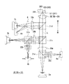
図1は、第1の実施の形態における光ピックアップ装置1の概略構成図である。
この図に示すように、光ピックアップ装置1は、レーザー光を出射する第1光源2aと第2光源2bとを備えている。
<First Embodiment>
First, an embodiment of an optical pickup device according to the present invention will be described.
FIG. 1 is a schematic configuration diagram of an
As shown in this figure, the
第1光源2aは波長λ1の第1光束を出射するものであり、波長λ1は380[nm]≦λ1≦450[nm]、本実施の形態においてはλ1=405[nm]となっている。この波長λ1は、AOD(情報記録媒体)100に対する使用波長である。なお、AOD100の保護基板101の厚さt1は、0.5[mm]≦t1≦0.7[mm]となっている。
第2光源2bは波長λ2の第2光束を出射するものであり、波長λ2は640[nm]≦λ2≦680[nm]、本実施の形態においてはλ2=650[nm]となっている。この波長λ2は、DVD(情報記録媒体)200に対する使用波長である。なお、DVD200の保護基板201の厚さt2は、0.5[mm]≦t2≦0.7[mm]となっている。
The first
The second
これら第1光源2a、第2光源2bから出射される各光束は、集光光学系3によってAOD100、DVD200に集光されるようになっている。
集光光学系3は、第1,第2コリメートレンズ30a,30bと、第1〜第3ビームスプリッタ31a〜31cと、対物レンズ(光学素子)5とを有している。
第1,第2コリメートレンズ30a,30bは、第1,第2光源2a,2bから出射される光束を平行光とするようになっている。
The light beams emitted from the first
The condensing
The first and second
ビームスプリッタ31aは、第1光源2aから出射される第1光束を対物レンズ5の方向へ透過させるとともに、AOD100からの反射光、つまり戻り光を第1光検出器4aに導くようになっている。ビームスプリッタ31aと第1光検出器4aとの間には、センサーレンズ群33aが配設されている。
ビームスプリッタ31bは、第2光源2bから出射される第2光束をビームスプリッタ31cの方向へ透過させるとともに、DVD200からの反射光を第2光検出器4bに導くようになっている。ビームスプリッタ31bと第2光検出器4bとの間には、センサーレンズ群33bが配設されている。
ビームスプリッタ31cは第1光源2aからの第1光束と、第2光源2bからの第2光束とを同一の光路にのせるようになっている。
The
The
The
対物レンズ5は、図2に示すように、レンズ本体(光学素子本体)50と反射防止膜51とを備え、所定の方向に移動可能な2次元アクチュエータ(図示せず)に搭載されている。対物レンズ5の開口数NAは0.65、光学機能面52,53における波長λ1の光束の最大入出射角度θmaxは0[°]≦θmax≦40[°]となっている。
As shown in FIG. 2, the
レンズ本体50は、プラスチックまたはガラスによって形成され、屈折率n0が1.45≦n0≦1.65となっている。
ここで、レンズ本体50に用いられるプラスチックとしては、ポリカーボネート樹脂やポリメチルメタクリレート樹脂、ノルボルネン系樹脂、脂環式オレフィン系樹脂などの光学プラスチックを用いることができる。なお、ノルボルネン系樹脂としては、ポリオレフィン系のものを用いることが好ましい。また、レンズ本体50に用いられるガラスとしては、低融点ガラスモールド用硝材を用いることができ、具体的にはM−BaCD5(商品名、HOYA製)などを用いることができる。
The
Here, as the plastic used for the
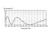
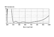
反射防止膜51は、レンズ本体50の少なくとも一方の面、本実施の形態においては両面に設けられ、光学機能面52,53を形成している。光学機能面52,53に垂直に入射する光束の反射率は、波長λ1と波長λ2との間で1[%]以上の極大値を示し、波長λ1及び波長λ2で相対的に低くなっている。従って、第1光束及び第2光束に対しては光学機能面52,53での反射が防止された状態となっている。
この反射防止膜51は、波長500[nm]の光束に対する屈折率nが
1.3≦n≦1.55である低屈折率材料と、
1.7≦n≦2.5である高屈折率材料とのうち、少なくとも2種類の材料から2層以上30層以下で構成されている。ここで、低屈折率材料としては、MgF2またはSiO2を主成分とする材料を用いることができる。また、高屈折率材料としては、TiO2、Ta2O5、CeO2、ZrO2、HfO2またはCeF3を主成分とする材料を用いることができる。また、反射防止膜51の形成には、蒸着やスパッタリング、CVD、塗布などの方法が用いられている。
The
The
Of the high refractive index material satisfying 1.7 ≦ n ≦ 2.5, it is composed of at least two layers and not less than 30 layers. Here, as the low refractive index material, a material mainly composed of MgF 2 or SiO 2 can be used. As the high refractive index material, a material mainly composed of TiO 2 , Ta 2 O 5 , CeO 2 , ZrO 2 , HfO 2 or CeF 3 can be used. Further, for the formation of the
また、反射防止膜51に含まれる層を、レンズ本体50に近い側から順に第1層、第2層、…第n層とすると、第1層の屈折率n1及び光学膜厚nd1と、第2層の屈折率n2及び光学膜厚nd2とは、
1.7≦n1≦2.5、225[nm]≦nd1≦275[nm]
1.3≦n2≦1.55、100[nm]≦nd2≦150[nm]
となっている。
Further, the layers included in the
1.7 ≦ n 1 ≦ 2.5, 225 [nm] ≦ nd 1 ≦ 275 [nm]
1.3 ≦ n 2 ≦ 1.55, 100 [nm] ≦ nd 2 ≦ 150 [nm]
It has become.
なお、レンズ本体50と反射防止膜51との間には下地層(図示せず)を介在させることが好ましい。この場合には、レンズ本体50に対する反射防止膜51の密着性を向上させることができる。更に、この下地層の屈折率n0’は、レンズ本体50の屈折率n0に対して、|n0’−n0|≦0.1とすることが好ましい。この場合には、下地層を設けることによる光学機能の劣化が防止された状態となる。
In addition, it is preferable to interpose a base layer (not shown) between the
以上のように構成された光ピックアップ装置1の動作については周知であるため詳しい説明は省略するが、第1光源2aから出射された第1光束は、第1ビームスプリッタ31aを通過した後、第1コリメートレンズ30aにおいて平行光化され、第3ビームスプリッタ31cを通過する。
Since the operation of the
次に、第1光束は対物レンズ5によってAOD100の情報記録面上に集光され、光軸L上にスポットを形成する。スポットを形成した第1光束は情報記録面で情報ピットにより変調されて反射され、再び対物レンズ5を通過する。ここで、光学機能面52,53における第1光束の反射は反射防止膜51によって防止されているので、第1光束は光量を低下させずに対物レンズ5を通過する。
次に、第1光束は第3ビームスプリッタ31c、第1コリメートレンズ30aを通過して、第1ビームスプリッタ31aで反射して分岐される。
そして、分岐された第1光束はセンサーレンズ群33aを経て第1光検出器4aに入射する。第1光検出器4aは入射光のスポットを検出して信号を出力し、その出力された信号を用いてAOD100に記録された情報の読み取り信号を得る。
Next, the first light beam is condensed on the information recording surface of the
Next, the first light beam passes through the
And the branched 1st light beam injects into the
また、第1光検出器4a上でのスポットの形状変化や位置変化による光量変化等を検出して合焦検出やトラック検出が行われる。この検出結果に基づいて前記2次元アクチュエータは、第1光束が情報記録面上に正確にスポットを形成するように、対物レンズ5をフォーカス方向及びトラッキング方向に移動させる。
In addition, focus detection and track detection are performed by detecting a change in the amount of light due to a change in the shape of the spot or a change in position on the
一方、第2光源2bから出射される第2光束は、第2ビームスプリッタ31bを通過した後、第2コリメートレンズ30bにおいて平行光化され、第3ビームスプリッタ31cで反射され、対物レンズ5に至る。
On the other hand, after passing through the
次に、第2光束は対物レンズ5によってDVD200の情報記録面上に集光され、光軸L上にスポットを形成する。スポットを形成した第2光束は情報記録面で情報ピットにより変調されて反射され、再び対物レンズ5を通過する。ここで、光学機能面52,53における第2光束の反射は反射防止膜51によって防止されているので、第2光束は光量を低下させずに対物レンズ5を通過する。
次に、第2光束は第3ビームスプリッタ31cで反射して分岐される。
そして、分岐された第2光束は第2コリメートレンズ30bを通過して、第2ビームスプリッタ31bで反射して分岐され、センサーレンズ群33aを経て第2光検出器4bに入射する。以下は第1光束の場合と同様である。
Next, the second light beam is condensed on the information recording surface of the
Next, the second light beam is reflected by the
The branched second light beam passes through the
以上のような光ピックアップ装置1によれば、波長λ1〜λ2の広い波長域の光束全体に対して反射を防止する従来の反射防止膜と異なり、第1光束及び第2光束に対する反射防止機能を損なうことなく、反射防止膜51の層数を少なくすることができる。従って、生産コストを低廉化することができるとともに、反射防止膜51の層と層との間に水分が浸透することによる分光特性の変化を抑えることができる。
また、レンズ本体50が光学プラスチック製である場合であっても、反射防止膜51の応力によって反射防止膜51にクラックが発生したり、反射防止膜51とレンズ本体50との密着性が低下したりすることを防ぐことができる、つまり耐環境性を向上させることができる。
According to the
Further, even when the
なお、上記実施の形態においては、第2光源の波長を640[nm]以上、680[nm]以下として説明したが、750[nm]以上、850[nm]以下としても良い。この場合には、情報記録媒体としてDVD200に代えてCDを用いることができる。
In the above embodiment, the wavelength of the second light source has been described as being 640 [nm] or more and 680 [nm] or less, but may be 750 [nm] or more and 850 [nm] or less. In this case, a CD can be used instead of the
<第2の実施の形態>
次に、本発明に係る光ピックアップ装置の第2の実施の形態について説明する。なお、上記第1の実施の形態と同様の構成要素には同一の符号を付し、その説明を省略する。
<Second Embodiment>
Next, a second embodiment of the optical pickup device according to the present invention will be described. In addition, the same code | symbol is attached | subjected to the component similar to the said 1st Embodiment, and the description is abbreviate | omitted.
本第2の実施の形態における光ピックアップ装置1Aは、上記第1の光ピックアップ装置1と異なり、対物レンズ5の代わりに対物レンズ5Aを備えている。
Unlike the first
対物レンズ5Aは、図2に示すように、レンズ本体50と、反射防止膜51Aとを備えている。
反射防止膜51Aは、レンズ本体50の少なくとも一方の面、本実施の形態においては両面に設けられ、光学機能面52A,53Aを形成している。光学機能面52A,53Aに垂直に入射する光束の反射率は、波長λ1と波長λ2との間で1[%]以上の極大値を示し、波長λ1及び波長λ2で相対的に低くなっている。従って、第1光束及び第2光束に対しては光学機能面52A,53Aでの反射が防止された状態となっている。
この反射防止膜51Aは、波長500[nm]の光束に対する屈折率nが
1.3≦n<1.55である低屈折率材料と、
1.55≦n<1.7である中屈折率材料と、
1.7≦n<2.5である高屈折率材料とのうち、少なくとも3種類の材料から3層以上30層以下で形成されている。ここで、低屈折率材料としては、MgF2またはSiO2を主成分とする材料を用いることができる。また、中屈折率材料としては、Al2O3を主成分とする材料を用いることができる。また、高屈折率材料としては、TiO2、Ta2O5、CeO2、ZrO2、HfO2またはCeF3を主成分とする材料を用いることができる。
As shown in FIG. 2, the
The
The
A medium refractive index material with 1.55 ≦ n <1.7;
Of the high refractive index material satisfying 1.7 ≦ n <2.5, it is formed of at least three kinds of materials and not less than three layers and not more than 30 layers. Here, as the low refractive index material, a material mainly composed of MgF 2 or SiO 2 can be used. Further, as the medium refractive index material, a material mainly composed of Al 2 O 3 can be used. As the high refractive index material, a material mainly composed of TiO 2 , Ta 2 O 5 , CeO 2 , ZrO 2 , HfO 2 or CeF 3 can be used.
また、反射防止膜51Aに含まれる層のうち、第1層の屈折率n1及び膜厚nd1と、第2層の屈折率n2及び膜厚nd2と、第3層の屈折率n3及び膜厚nd3とは、
1.7≦n1≦2.5、125[nm]≦nd1≦175[nm]、
1.55≦n2<1.7、75[nm]≦nd2≦125[nm]、
1.3≦n3<1.55、100[nm]≦nd3≦150[nm]、
となっている。
Among the layers included in the
1.7 ≦ n 1 ≦ 2.5, 125 [nm] ≦ nd 1 ≦ 175 [nm],
1.55 ≦ n 2 <1.7, 75 [nm] ≦ nd 2 ≦ 125 [nm],
1.3 ≦ n 3 <1.55, 100 [nm] ≦ nd 3 ≦ 150 [nm],
It has become.
以上のような光ピックアップ装置1Aの動作は、上記第1の実施の形態における光ピックアップ装置1の動作と同様である。
この光ピックアップ装置1Aによっても、上記第1の実施の形態と同様の効果を得ることができる。
The operation of the
Also with this
<第3の実施の形態>
次に、本発明に係る光ピックアップ装置の第3の実施の形態について説明する。なお、上記第1の実施の形態と同様の構成要素には同一の符号を付し、その説明を省略する。
<Third Embodiment>
Next, a third embodiment of the optical pickup device according to the present invention will be described. In addition, the same code | symbol is attached | subjected to the component similar to the said 1st Embodiment, and the description is abbreviate | omitted.
図3は、第2の実施の形態における光ピックアップ装置1Bの概略構成図である。
この図に示すように、光ピックアップ装置1Bは、上記第1の実施の形態における光ピックアップ装置1と異なり、更に第3光源2c、コリメータレンズ30c、ビームスプリッタ31d及び回折板6を備え、かつ、前記対物レンズ5の代わりに対物レンズ5Bを備えている。
FIG. 3 is a schematic configuration diagram of an
As shown in this figure, the
第3光源2cは波長λ3の第3光束を出射するものであり、波長λ3は750[nm]≦λ3≦850[nm]、本実施の形態においてはλ3=780[nm]となっている。この波長λ3は、CD(第3光情報記録媒体)300に対する使用波長である。なお、CD300の保護基板301の厚さt3は、1.1[mm]≦t3≦1.3[mm]となっている。
第3コリメートレンズ30cは、第3光源2cから出射される光束を平行光とするようになっている。
ビームスプリッタ31dは、第3光源2cからの第3光束と、ビームスプリッタ31cを透過した第1光束及び第2光束とを同一の光路にのせるようになっている。ビームスプリッタ31dと第3光源2cとの間には、CD300からの反射光を第3光検出器4cに導く回折板6が配設されている。
The third
The
The
対物レンズ5Bは、図2に示すように、レンズ本体(光学素子本体)50Bと、第1光束、第2光束及び第3光束に対して反射防止機能を有する反射防止膜51Bとを備えている。
反射防止膜51Bは、レンズ本体50の少なくとも一方の面、本実施の形態においては両面に設けられ、光学機能面52B,53Bを形成している。光学機能面52B,53Bに垂直に入射する光束の反射率は、波長λ1と波長λ2との間で1[%]以上の極大値を示し、波長λ1及び波長λ2で相対的に低くなっている。従って、第1光束及び第2光束に対しては光学機能面52B,53Bでの反射が防止された状態となっている。
この反射防止膜51Bは、波長500[nm]の光束に対する屈折率nが
1.3≦n≦1.55である低屈折率材料と、
1.7≦n≦2.5である高屈折率材料とのうち、少なくとも2種類の材料から4層以上30層以下で形成されている。
As shown in FIG. 2, the objective lens 5B includes a lens body (optical element body) 50B and an antireflection film 51B having an antireflection function for the first light beam, the second light beam, and the third light beam. .
The antireflection film 51B is provided on at least one surface of the lens
The antireflection film 51B includes a low refractive index material having a refractive index n of 1.3 ≦ n ≦ 1.55 for a light beam having a wavelength of 500 [nm], and
Among the high refractive index materials satisfying 1.7 ≦ n ≦ 2.5, the layers are formed of at least two types of materials and not less than 4 layers and not more than 30 layers.
また、反射防止膜51Bに含まれる層のうち、第1層の屈折率n1及び光学膜厚nd1と、第2層の屈折率n2及び光学膜厚nd2と、第3層の屈折率n3及び光学膜厚nd3と、第4層の屈折率n4及び光学膜厚nd4とは、
1.7≦n1≦2.5、25[nm]≦nd1≦75[nm]、
1.3≦n2≦1.55、25[nm]≦nd2≦75[nm]、
1.7≦n3≦2.5、225[nm]≦nd3≦275[nm]、
1.3≦n4≦1.55、135[nm]≦nd4≦185[nm]
となっている。
Of the layers included in the antireflection film 51B, the refractive index n 1 and the optical film thickness nd 1 of the first layer, the refractive index n 2 and the optical film thickness nd 2 of the second layer, and the refraction of the third layer. a rate n 3 and the optical thickness nd 3, the refractive index n 4 and the optical thickness nd 4 of the fourth layer,
1.7 ≦ n 1 ≦ 2.5, 25 [nm] ≦ nd 1 ≦ 75 [nm],
1.3 ≦ n 2 ≦ 1.55, 25 [nm] ≦ nd 2 ≦ 75 [nm],
1.7 ≦ n 3 ≦ 2.5, 225 [nm] ≦ nd 3 ≦ 275 [nm],
1.3 ≦ n 4 ≦ 1.55, 135 [nm] ≦ nd 4 ≦ 185 [nm]
It has become.
以上のように構成された光ピックアップ装置1Bの動作のうち、AOD100及びDVD200を用いた記録及び/または再生については、上記第1の実施の形態における光ピックアップ装置1と同様である。
また、光ピックアップ装置1Bの動作のうち、CD300を用いた記録及び/または再生においては、まず、第3光源2cから出射された第3光束は、回折板6を通過した後、第3コリメートレンズ30cにおいて平行光化され、第4ビームスプリッタ31dで反射され、対物レンズ5に至る。
Of the operations of the
In the recording and / or reproduction using the
次に、第3光束は対物レンズ5によってCD300の情報記録面上に集光され、光軸L上にスポットを形成する。スポットを形成した第3光束は情報記録面で情報ピットにより変調されて反射され、再び対物レンズ5を通過する。ここで、反射防止膜51によって光学機能面52,53における第2光束の反射が防止されているので、第3光束は光量を低下させずに対物レンズ5を通過する。
次に、第3光束は、第4ビームスプリッタ31dで反射して分岐される。
そして、分岐された第3光束は第3コリメートレンズ30cを通過して、回折板6を通過する際に進路を変更され、第3光検出器4cに入射する。以下は第1光束の場合と同様である。
Next, the third light beam is condensed on the information recording surface of the
Next, the third light flux is reflected by the
Then, the branched third light beam passes through the
以上のような光ピックアップ装置1Bによれば、波長λ1〜λ3の広い波長域の光束全体に対して反射を防止する従来の反射防止膜と異なり、第1光束、第2光束及び第3光束に対する反射防止機能を損なうことなく、反射防止膜51Bの層数を少なくすることができる。従って、生産コストを低廉化することができるとともに、反射防止膜51Bの層と層との間に水分が浸透することによる分光特性の変化を抑えることができる。
また、レンズ本体50が光学プラスチック製である場合であっても、反射防止膜51Bの応力によって反射防止膜51Bにクラックが発生したり、反射防止膜51Bとレンズ本体50との密着性が低下したりすることを防ぐことができる、つまり耐環境性を向上させることができる。
According to the
Even when the
<第4の実施の形態>
本第4の実施の形態における光ピックアップ装置1Cは、上記第1の光ピックアップ装置1と異なり、対物レンズ5の代わりに対物レンズ5Cを備えている。
対物レンズ5Cは、図2に示すように、レンズ本体50と、反射防止膜51Cとを備えている。
<Fourth embodiment>
Unlike the first
As shown in FIG. 2, the objective lens 5C includes a
反射防止膜51Cは、レンズ本体50の少なくとも一方の面、本実施の形態においては両面に設けられ、光学機能面52C,53Cを形成している。より詳細には、反射防止膜51Cは、{(第1光束に対する有効径内での最大膜厚)−(この有効径内での最小膜厚)}/平均膜厚の値が5[%]以下となるように成膜されている。つまり、反射防止膜5Cの膜厚は、ほぼ均一とされている。
光学機能面52C,53Cは、前記有効径内での最大入出射角度θmaxが0[°]≦θmax≦40[°]となっている。また、光学機能面52C,53Cは、垂直に入射する光束の波長λがλ1≦λ≦λ1+15[nm]である場合と、λ2≦λ≦λ2+15[nm]である場合とには、反射率を1[%]以下に抑えるようになっている。また、光学機能面52C,53Cは、前記波長λがλ1+15[nm]<λ<λ2の範囲内の或る波長である場合に、反射率が1[%]よりも大きい極大値を示すようになっている。
The antireflection film 51C is provided on at least one surface of the lens
The optical function surfaces 52C and 53C have a maximum incident / exit angle θmax within the effective diameter of 0 [°] ≦ θmax ≦ 40 [°]. Further, the optical function surfaces 52C and 53C have reflectivity when the wavelength λ of the vertically incident light beam is λ1 ≦ λ ≦ λ1 + 15 [nm] and when λ2 ≦ λ ≦ λ2 + 15 [nm]. 1 [%] or less. Further, the optical functional surfaces 52C and 53C exhibit a maximum value with a reflectance larger than 1 [%] when the wavelength λ is a certain wavelength within the range of λ1 + 15 [nm] <λ <λ2. It has become.
以上の光ピックアップ装置1Cの動作は、上記第1の実施の形態における光ピックアップ装置1と同様である。
この光ピックアップ装置1Cによれば、光学機能面52C,53Cに垂直に入射する光束の波長λがλ1≦λ≦λ1+15[nm]である場合と、λ2≦λ≦λ2+15[nm]である場合とには、光学機能面52C,53Cにおける反射率が1[%]以下であるので、これらの帯域内の波長に対しては反射を防止することができる。また、波長λがλ1+15[nm]<λ<λ2の範囲内の或る波長である場合に、反射率が1[%]よりも大きい極大値を示す、つまり反射防止機能が低下するので、波長λ1〜λ2の広い波長域の光束全体に対して反射を防止する従来の反射防止膜と異なり、第1光束と第2光束とに対する反射防止機能を損なうことなく、反射防止膜51Cの層数を少なくすることができる。従って、生産コストを低廉化することができるとともに、反射防止膜51Cの層と層との間に水分が浸透することによる分光特性の変化を抑えることができる。
また、レンズ本体50が光学プラスチック製である場合であっても、反射防止膜51Cの応力によって反射防止膜51Cにクラックが発生したり、反射防止膜51Cとレンズ本体50との密着性が低下したりすることを防ぐことができる、つまり耐環境性を向上させることができる。
The operation of the optical pickup device 1C described above is the same as that of the
According to the optical pickup device 1C, the wavelength λ of the light beam perpendicularly incident on the optical functional surfaces 52C and 53C is λ1 ≦ λ ≦ λ1 + 15 [nm], and the case where λ2 ≦ λ ≦ λ2 + 15 [nm]. Since the reflectance at the optical functional surfaces 52C and 53C is 1% or less, reflection can be prevented for wavelengths within these bands. Further, when the wavelength λ is a certain wavelength within the range of λ1 + 15 [nm] <λ <λ2, the reflectance shows a maximum value larger than 1 [%], that is, the antireflection function is lowered. Unlike the conventional antireflection film that prevents reflection of the entire light flux in a wide wavelength range of λ1 to λ2, the number of layers of the antireflection film 51C is reduced without impairing the antireflection function for the first light flux and the second light flux. Can be reduced. Therefore, the production cost can be reduced, and the change in the spectral characteristics due to the penetration of moisture between the layers of the antireflection film 51C can be suppressed.
Even when the
<第5の実施の形態>
本第5の実施の形態における光ピックアップ装置1Dは、上記第1の光ピックアップ装置1と異なり、対物レンズ5の代わりに対物レンズ5Dを備えている。
対物レンズ5Dは、図2に示すように、レンズ本体50と、反射防止膜51Dとを備えている。
<Fifth embodiment>
Unlike the first
As shown in FIG. 2, the objective lens 5D includes a
反射防止膜51Dは、レンズ本体50の少なくとも一方の面、本実施の形態においては両面に設けられ、光学機能面52D,53Dを形成している。より詳細には、反射防止膜51Dは、{(第1光束に対する有効径内での最大膜厚)−(この有効径内での最小膜厚)}/平均膜厚の値が5[%]以下となるように成膜されている。つまり、反射防止膜5Dの膜厚は、ほぼ均一とされている。
光学機能面52D,53Dは、前記有効径内での最大入出射角度θmaxが40[°]<θmax<90[°]となっている。また、光学機能面52D,53Dは、垂直に入射する光束の波長λがλ1≦λ≦λ1+50[nm]である場合と、λ2≦λ≦λ2+40[nm]である場合とには、反射率を1[%]以下に抑えるようになっている。また、光学機能面52D,53Dは、前記波長λがλ1+50[nm]<λ<λ2の範囲内の或る波長である場合に、反射率が1[%]よりも大きい極大値を示すようになっている。
The antireflection film 51D is provided on at least one surface of the
The optical function surfaces 52D and 53D have a maximum incident / exit angle θmax within the effective diameter of 40 [°] <θmax <90 [°]. Further, the optical function surfaces 52D and 53D have reflectivity when the wavelength λ of the vertically incident light beam is λ1 ≦ λ ≦ λ1 + 50 [nm] and when λ2 ≦ λ ≦ λ2 + 40 [nm]. 1 [%] or less. Further, the optical functional surfaces 52D and 53D exhibit a maximum value with a reflectance larger than 1 [%] when the wavelength λ is a certain wavelength within the range of λ1 + 50 [nm] <λ <λ2. It has become.
以上の光ピックアップ装置1Dの動作は、上記第1の実施の形態における光ピックアップ装置1と同様である。
この光ピックアップ装置1Dによれば、光学機能面52D,53Dに垂直に入射する光束の波長λがλ1≦λ≦λ1+50[nm]である場合と、λ2≦λ≦λ2+40[nm]である場合とには、光学機能面52D,53Dにおける反射率が1[%]以下であるので、これらの帯域内の波長に対しては反射を防止することができる。また、波長λがλ1+50[nm]<λ<λ2の範囲内の或る波長である場合に、反射率が1[%]よりも大きい極大値を示す、つまり反射防止機能が低下するので、波長λ1〜λ2の広い波長域の光束全体に対して反射を防止する従来の反射防止膜と異なり、第1光束と第2光束とに対する反射防止機能を損なうことなく、反射防止膜51Dの層数を少なくすることができる。従って、生産コストを低廉化することができるとともに、反射防止膜51Dの層と層との間に水分が浸透することによる分光特性の変化を抑えることができる。
また、レンズ本体50が光学プラスチック製である場合であっても、反射防止膜51Dの応力によって反射防止膜51Dにクラックが発生したり、反射防止膜51Dとレンズ本体50との密着性が低下したりすることを防ぐことができる、つまり耐環境性を向上させることができる。
The operation of the optical pickup device 1D described above is the same as that of the
According to the optical pickup device 1D, the wavelength λ of the light beam perpendicularly incident on the optical function surfaces 52D and 53D is λ1 ≦ λ ≦ λ1 + 50 [nm], and λ2 ≦ λ ≦ λ2 + 40 [nm]. Since the reflectance at the optical functional surfaces 52D and 53D is 1% or less, reflection can be prevented for wavelengths within these bands. Further, when the wavelength λ is a certain wavelength within the range of λ1 + 50 [nm] <λ <λ2, the reflectance shows a maximum value larger than 1 [%], that is, the antireflection function is lowered. Unlike a conventional antireflection film that prevents reflection of the entire light flux in a wide wavelength range of λ1 to λ2, the number of layers of the antireflection film 51D is reduced without impairing the antireflection function for the first light flux and the second light flux. Can be reduced. Therefore, it is possible to reduce the production cost and to suppress the change in spectral characteristics due to the permeation of moisture between the layers of the antireflection film 51D.
Even when the
<第6の実施の形態>
本第6の実施の形態における光ピックアップ装置1Eは、上記第1の光ピックアップ装置1と異なり、対物レンズ5の代わりに対物レンズ5Eを備えている。
対物レンズ5Eは、図2に示すように、レンズ本体50と、反射防止膜51Eとを備えている。
<Sixth Embodiment>
Unlike the first
As shown in FIG. 2, the objective lens 5E includes a
反射防止膜51Eは、レンズ本体50の少なくとも一方の面、本実施の形態においては両面に設けられ、光学機能面52E,53Eを形成している。より詳細には、反射防止膜51Eは、{(第1光束に対する有効径内での最大膜厚)−(この有効径内での最小膜厚)}/平均膜厚の値が5[%]以下となるように成膜されている。つまり、反射防止膜5Eの膜厚は、ほぼ均一とされている。
光学機能面52Eは、前記有効径内での最大入出射角度θmaxが40[°]<θmax<90[°]となっている。また、光学機能面52Eは、垂直に入射する光束の波長λがλ1≦λ≦λ1+50[nm]である場合と、λ2≦λ≦λ2+40[nm]である場合とには、反射率を1[%]以下に抑えるようになっている。また、光学機能面52Eは、前記波長λがλ1+50[nm]<λ<λ2の範囲内の或る波長である場合に、反射率が1[%]よりも大きい極大値を示すようになっている。
光学機能面53Eは、前記有効径内での最大入出射角度θmaxが0[°]≦θmax≦40[°]となっている。また、光学機能面53Eは、垂直に入射する光束の波長λがλ1≦λ≦λ1+15[nm]である場合と、λ2≦λ≦λ2+15[nm]である場合とには、反射率を1[%]以下に抑えるようになっている。また、光学機能面53Eは、前記波長λがλ1+15[nm]<λ<λ2の範囲内の或る波長である場合に、反射率が1[%]よりも大きい極大値を示すようになっている。
The antireflection film 51E is provided on at least one surface of the
The optical function surface 52E has a maximum incident / exit angle θmax within the effective diameter of 40 [°] <θmax <90 [°]. The optical function surface 52E has a reflectance of 1 [1] when the wavelength λ of the vertically incident light beam is λ1 ≦ λ ≦ λ1 + 50 [nm] and when λ2 ≦ λ ≦ λ2 + 40 [nm]. %] Or less. Further, the optical functional surface 52E exhibits a maximum value with a reflectance larger than 1 [%] when the wavelength λ is a certain wavelength within the range of λ1 + 50 [nm] <λ <λ2. Yes.
The optical function surface 53E has a maximum incident / exit angle θmax within the effective diameter of 0 [°] ≦ θmax ≦ 40 [°]. The optical function surface 53E has a reflectance of 1 [1] when the wavelength λ of the vertically incident light beam is λ1 ≦ λ ≦ λ1 + 15 [nm] and when λ2 ≦ λ ≦ λ2 + 15 [nm]. %] Or less. The optical function surface 53E exhibits a maximum value with a reflectance larger than 1% when the wavelength λ is a certain wavelength within the range of λ1 + 15 [nm] <λ <λ2. Yes.
以上の光ピックアップ装置1Eの動作は、上記第1の実施の形態における光ピックアップ装置1と同様である。
この光ピックアップ装置1Eによれば、光学機能面53Eに垂直に入射する光束の波長λがλ1≦λ≦λ1+15[nm]である場合と、λ2≦λ≦λ2+15[nm]である場合とには、光学機能面53Eにおける反射率が1[%]以下であり、光学機能面52Eに垂直に入射する光束の波長λがλ1≦λ≦λ1+50[nm]である場合と、λ2≦λ≦λ2+40[nm]である場合とには、光学機能面52Eにおける反射率が1[%]以下であるので、これらの帯域内の波長に対しては反射を防止することができる。また、光学機能面53Eにおいては、波長λがλ1+15[nm]<λ<λ2の範囲内の或る波長である場合に反射率が1[%]よりも大きい極大値を示し、光学機能面52Eにおいては、波長λがλ1+50[nm]<λ<λ2の範囲内の或る波長である場合に反射率が1[%]よりも大きい極大値を示す、つまり反射防止機能が低下するので、波長λ1〜λ2の広い波長域の光束全体に対して反射を防止する従来の反射防止膜と異なり、第1光束と第2光束とに対する反射防止機能を損なうことなく、反射防止膜51Eの層数を少なくすることができる。従って、生産コストを低廉化することができるとともに、反射防止膜51Eの層と層との間に水分が浸透することによる分光特性の変化を抑えることができる。
また、レンズ本体50が光学プラスチック製である場合であっても、反射防止膜51Eの応力によって反射防止膜51Eにクラックが発生したり、反射防止膜51Eとレンズ本体50との密着性が低下したりすることを防ぐことができる、つまり耐環境性を向上させることができる。
The operation of the optical pickup device 1E is the same as that of the
According to the optical pickup device 1E, when the wavelength λ of the light beam perpendicularly incident on the optical function surface 53E is λ1 ≦ λ ≦ λ1 + 15 [nm], and when λ2 ≦ λ ≦ λ2 + 15 [nm]. The reflectance at the optical functional surface 53E is 1% or less, and the wavelength λ of the light beam incident perpendicularly to the optical functional surface 52E is λ1 ≦ λ ≦ λ1 + 50 [nm], and λ2 ≦ λ ≦ λ2 + 40 [ In the case of [nm], since the reflectance at the optical functional surface 52E is 1% or less, reflection can be prevented for wavelengths within these bands. Further, the optical functional surface 53E exhibits a maximum value with a reflectance larger than 1 [%] when the wavelength λ is a certain wavelength within the range of λ1 + 15 [nm] <λ <λ2, and the optical functional surface 52E. In the case where the wavelength λ is a certain wavelength within the range of λ1 + 50 [nm] <λ <λ2, the reflectance shows a maximum value larger than 1 [%], that is, the antireflection function is lowered. Unlike the conventional antireflection film that prevents the reflection of the entire light beam in the wide wavelength range of λ1 to λ2, the number of layers of the antireflection film 51E is reduced without impairing the antireflection function for the first light beam and the second light beam. Can be reduced. Therefore, the production cost can be reduced, and the change in spectral characteristics due to the penetration of moisture between the layers of the antireflection film 51E can be suppressed.
Even when the
なお、本実施の形態においては、光学機能面52Eを光入射面、光学機能面53Eを光出射面として説明したが、光学機能面52Eを光出射面、光学機能面53Eを光出射面としても良い。 In the present embodiment, the optical function surface 52E is described as a light incident surface, and the optical function surface 53E is described as a light output surface. However, the optical function surface 52E may be a light output surface and the optical function surface 53E may be a light output surface. good.
<第7の実施の形態>
本第7の実施の形態における光ピックアップ装置1Fは、上記第1の光ピックアップ装置1と異なり、対物レンズ5の代わりに対物レンズ5Fを備えている。
対物レンズ5Fは、図2に示すように、レンズ本体50と、反射防止膜51Fとを備えている。
<Seventh embodiment>
Unlike the first
As shown in FIG. 2, the objective lens 5F includes a
反射防止膜51Fは、レンズ本体50の少なくとも一方の面、本実施の形態においては両面に設けられ、光学機能面52F,53Fを形成している。より詳細には、反射防止膜51Fは、{(第1光束に対する有効径内での最大膜厚)−(この有効径内での最小膜厚)}/平均膜厚の値が5[%]より大きくなるように成膜されている。つまり、反射防止膜5Fの膜厚は、不均一とされている。
光学機能面52F,53Fは、前記有効径内での最大入出射角度θmaxと、前記有効径内における最大面角度θ⊥maxとが0[°]≦θmax≦40[°]、かつ、0[°]≦θ⊥max≦40[°]となっている。また、光学機能面52F,53Fは、垂直に入射する光束の波長λがλ1≦λ≦λ1+15[nm]である場合と、λ2≦λ≦λ2+15[nm]である場合とには、反射率を1[%]以下に抑えるようになっている。また、光学機能面52F,53Fは、前記波長λがλ1+15[nm]<λ<λ2の範囲内の或る波長である場合に、反射率が1[%]よりも大きい極大値を示すようになっている。
The antireflection film 51F is provided on at least one surface of the
In the optical function surfaces 52F and 53F, the maximum incident / exit angle θmax within the effective diameter and the maximum surface angle θ⊥max within the effective diameter are 0 [°] ≦ θmax ≦ 40 [°] and 0 [ °] ≦ θ⊥max ≦ 40 [°]. Further, the optical function surfaces 52F and 53F have reflectivity when the wavelength λ of the vertically incident light beam is λ1 ≦ λ ≦ λ1 + 15 [nm] and when λ2 ≦ λ ≦ λ2 + 15 [nm]. 1 [%] or less. Further, the optical functional surfaces 52F and 53F exhibit a maximum value with a reflectance larger than 1 [%] when the wavelength λ is a certain wavelength within the range of λ1 + 15 [nm] <λ <λ2. It has become.
以上の光ピックアップ装置1Fの動作は、上記第1の実施の形態における光ピックアップ装置1と同様である。
この光ピックアップ装置1Fによれば、光学機能面52F,53Fに垂直に入射する光束の波長λがλ1≦λ≦λ1+15[nm]である場合と、λ2≦λ≦λ2+15[nm]である場合とには、光学機能面52F,53Fにおける反射率が1[%]以下であるので、これらの帯域内の波長に対しては反射を防止することができる。また、波長λがλ1+15[nm]<λ<λ2の範囲内の或る波長である場合に、反射率が1[%]よりも大きい極大値を示す、つまり反射防止機能が低下するので、波長λ1〜λ2の広い波長域の光束全体に対して反射を防止する従来の反射防止膜と異なり、第1光束と第2光束とに対する反射防止機能を損なうことなく、反射防止膜51Fの層数を少なくすることができる。従って、生産コストを低廉化することができるとともに、反射防止膜51Fの層と層との間に水分が浸透することによる分光特性の変化を抑えることができる。
また、レンズ本体50が光学プラスチック製である場合であっても、反射防止膜51Fの応力によって反射防止膜51Fにクラックが発生したり、反射防止膜51Fとレンズ本体50との密着性が低下したりすることを防ぐことができる、つまり耐環境性を向上させることができる。
The operation of the optical pickup device 1F described above is the same as that of the
According to the optical pickup device 1F, the wavelength λ of the light beam perpendicularly incident on the optical function surfaces 52F and 53F is λ1 ≦ λ ≦ λ1 + 15 [nm] and the case where λ2 ≦ λ ≦ λ2 + 15 [nm]. Since the reflectance at the optical functional surfaces 52F and 53F is 1% or less, reflection can be prevented for wavelengths in these bands. Further, when the wavelength λ is a certain wavelength within the range of λ1 + 15 [nm] <λ <λ2, the reflectance shows a maximum value larger than 1 [%], that is, the antireflection function is lowered. Unlike the conventional antireflection film that prevents reflection of the entire light flux in the wide wavelength range of λ1 to λ2, the number of layers of the antireflection film 51F is reduced without impairing the antireflection function for the first light flux and the second light flux. Can be reduced. Therefore, it is possible to reduce the production cost and to suppress the change in the spectral characteristics due to the penetration of moisture between the layers of the antireflection film 51F.
Even when the
<第8の実施の形態>
本第8の実施の形態における光ピックアップ装置1Gは、上記第1の光ピックアップ装置1と異なり、対物レンズ5の代わりに対物レンズ5Gを備えている。
対物レンズ5Gは、図2に示すように、レンズ本体50と、反射防止膜51Gとを備えている。
<Eighth Embodiment>
Unlike the first
As shown in FIG. 2, the objective lens 5G includes a
反射防止膜51Gは、レンズ本体50の少なくとも一方の面、本実施の形態においては両面に設けられ、光学機能面52G,53Gを形成している。より詳細には、反射防止膜51Gは、{(第1光束に対する有効径内での最大膜厚)−(この有効径内での最小膜厚)}/平均膜厚の値が5[%]より大きくなるように成膜されている。つまり、反射防止膜5Gの膜厚は、不均一とされている。
光学機能面52G,53Gは、前記有効径内での最大入出射角度θmaxと、前記有効径内における最大面角度θ⊥maxとが
0[°]≦θmax≦40[°]、かつ、40[°]<θ⊥max<90[°]
または40[°]<θmax<90[°]、かつ、0[°]≦θ⊥max≦40[°]となっている。また、光学機能面52G,53Gは、垂直に入射する光束の波長λがλ1≦λ≦λ1+50[nm]である場合と、λ2≦λ≦λ2+40[nm]である場合とには、反射率を1[%]以下に抑えるようになっている。また、光学機能面52G,53Gは、前記波長λがλ1+50[nm]<λ<λ2の範囲内の或る波長である場合に、反射率が1[%]よりも大きい極大値を示すようになっている。
The antireflection film 51G is provided on at least one surface of the
The optical function surfaces 52G and 53G have a maximum incident / exit angle θmax within the effective diameter and a maximum surface angle θ⊥max within the effective diameter of 0 [°] ≦ θmax ≦ 40 [°] and 40 [ °] <θ⊥max <90 [°]
Alternatively, 40 [°] <θmax <90 [°] and 0 [°] ≦ θ⊥max ≦ 40 [°]. The optical function surfaces 52G and 53G have a reflectance when the wavelength λ of the vertically incident light beam is λ1 ≦ λ ≦ λ1 + 50 [nm] and when λ2 ≦ λ ≦ λ2 + 40 [nm]. 1 [%] or less. Further, the optical functional surfaces 52G and 53G exhibit a maximum value with a reflectance larger than 1 [%] when the wavelength λ is a certain wavelength within the range of λ1 + 50 [nm] <λ <λ2. It has become.
以上の光ピックアップ装置1Gの動作は、上記第1の実施の形態における光ピックアップ装置1と同様である。
この光ピックアップ装置1Gによれば、光学機能面52G,53Gに垂直に入射する光束の波長λがλ1≦λ≦λ1+50[nm]である場合と、λ2≦λ≦λ2+40[nm]である場合とには、光学機能面52G,53Gにおける反射率が1[%]以下であるので、これらの帯域内の波長に対しては反射を防止することができる。また、波長λがλ1+50[nm]<λ<λ2の範囲内の或る波長である場合に、反射率が1[%]よりも大きい極大値を示す、つまり反射防止機能が低下するので、波長λ1〜λ2の広い波長域の光束全体に対して反射を防止する従来の反射防止膜と異なり、第1光束と第2光束とに対する反射防止機能を損なうことなく、反射防止膜51Gの層数を少なくすることができる。従って、生産コストを低廉化することができるとともに、反射防止膜51Gの層と層との間に水分が浸透することによる分光特性の変化を抑えることができる。
また、レンズ本体50が光学プラスチック製である場合であっても、反射防止膜51Gの応力によって反射防止膜51Gにクラックが発生したり、反射防止膜51Gとレンズ本体50との密着性が低下したりすることを防ぐことができる、つまり耐環境性を向上させることができる。
The operation of the optical pickup device 1G described above is the same as that of the
According to the optical pickup device 1G, the wavelength λ of the light beam perpendicularly incident on the optical function surfaces 52G and 53G is λ1 ≦ λ ≦ λ1 + 50 [nm], and λ2 ≦ λ ≦ λ2 + 40 [nm]. Since the reflectance at the optical functional surfaces 52G and 53G is 1% or less, reflection can be prevented for wavelengths within these bands. Further, when the wavelength λ is a certain wavelength within the range of λ1 + 50 [nm] <λ <λ2, the reflectance shows a maximum value larger than 1 [%], that is, the antireflection function is lowered. Unlike the conventional antireflection film that prevents reflection of the entire light flux in a wide wavelength range of λ1 to λ2, the number of layers of the antireflection film 51G is reduced without impairing the antireflection function for the first light flux and the second light flux. Can be reduced. Therefore, the production cost can be reduced, and the change in the spectral characteristics due to the penetration of moisture between the layers of the antireflection film 51G can be suppressed.
Even when the
<第9の実施の形態>
本第9の実施の形態における光ピックアップ装置1Iは、上記第1の光ピックアップ装置1と異なり、対物レンズ5の代わりに対物レンズ5Iを備えている。
対物レンズ5Iは、図2に示すように、レンズ本体50と、反射防止膜51Iとを備えている。
<Ninth embodiment>
Unlike the first
As shown in FIG. 2, the objective lens 5I includes a
反射防止膜51Iは、レンズ本体50の少なくとも一方の面、本実施の形態においては両面に設けられ、光学機能面52I,53Iを形成している。より詳細には、反射防止膜51Iは、{(第1光束に対する有効径内での最大膜厚)−(この有効径内での最小膜厚)}/平均膜厚の値が5[%]より大きくなるように成膜されている。つまり、反射防止膜5Iの膜厚は、不均一とされている。
光学機能面52Iは、有効径内での最大入出射角度θmaxと、前記有効径内における最大面角度θ⊥maxとが
0[°]≦θmax≦40[°]、かつ、40[°]<θ⊥max<90[°]
または40[°]<θmax<90[°]、かつ、0[°]≦θ⊥max≦40[°]となっている。また、光学機能面52Iは、垂直に入射する光束の波長λがλ1≦λ≦λ1+50[nm]である場合と、λ2≦λ≦λ2+40[nm]である場合とには、反射率を1[%]以下に抑えるようになっている。また、光学機能面52Iは、前記波長λがλ1+50[nm]<λ<λ2の範囲内の或る波長である場合に、反射率が1[%]よりも大きい極大値を示すようになっている。
光学機能面53Iは、有効径内での最大入出射角度θmaxと、前記有効径内における最大面角度θ⊥maxとが0[°]≦θmax≦40[°]、かつ、0[°]≦θ⊥max≦40[°]となっている。また、光学機能面53Iは、垂直に入射する光束の波長λがλ1≦λ≦λ1+15[nm]である場合と、λ2≦λ≦λ2+15[nm]である場合とには、反射率を1[%]以下に抑えるようになっている。また、光学機能面53Iは、前記波長λがλ1+15[nm]<λ<λ2の範囲内の或る波長である場合に、反射率が1[%]よりも大きい極大値を示すようになっている。
The antireflection film 51I is provided on at least one surface of the
The optical functional surface 52I has a maximum incident / exit angle θmax within the effective diameter and a maximum surface angle θ⊥max within the effective diameter of 0 [°] ≦ θmax ≦ 40 [°] and 40 [°] < θ⊥max <90 [°]
Alternatively, 40 [°] <θmax <90 [°] and 0 [°] ≦ θ⊥max ≦ 40 [°]. The optical function surface 52I has a reflectance of 1 [1] when the wavelength λ of the vertically incident light beam is λ1 ≦ λ ≦ λ1 + 50 [nm] and when λ2 ≦ λ ≦ λ2 + 40 [nm]. %] Or less. Further, the optical functional surface 52I exhibits a maximum value with a reflectance higher than 1 [%] when the wavelength λ is a certain wavelength within the range of λ1 + 50 [nm] <λ <λ2. Yes.
In the optical function surface 53I, the maximum incident / exit angle θmax within the effective diameter and the maximum surface angle θ⊥max within the effective diameter are 0 [°] ≦ θmax ≦ 40 [°] and 0 [°] ≦ θ⊥max ≦ 40 [°]. The optical function surface 53I has a reflectance of 1 [1] when the wavelength λ of the vertically incident light beam is λ1 ≦ λ ≦ λ1 + 15 [nm] and when λ2 ≦ λ ≦ λ2 + 15 [nm]. %] Or less. Further, the optical functional surface 53I exhibits a maximum value with a reflectance larger than 1% when the wavelength λ is a certain wavelength within the range of λ1 + 15 [nm] <λ <λ2. Yes.
以上の光ピックアップ装置1Iの動作は、上記第1の実施の形態における光ピックアップ装置1と同様である。
この光ピックアップ装置1Iによれば、光学機能面53Iに垂直に入射する光束の波長λがλ1≦λ≦λ1+15[nm]である場合と、λ2≦λ≦λ2+15[nm]である場合とには、光学機能面53Iにおける反射率が1[%]以下であり、光学機能面52Iに垂直に入射する光束の波長λがλ1≦λ≦λ1+50[nm]である場合と、λ2≦λ≦λ2+40[nm]である場合とには、光学機能面52Iにおける反射率が1[%]以下であるので、これらの帯域内の波長に対しては反射を防止することができる。また、光学機能面53Iにおいては、波長λがλ1+15[nm]<λ<λ2の範囲内の或る波長である場合に反射率が1[%]よりも大きい極大値を示し、光学機能面52Iにおいては、波長λがλ1+50[nm]<λ<λ2の範囲内の或る波長である場合に反射率が1[%]よりも大きい極大値を示す、つまり反射防止機能が低下するので、波長λ1〜λ2の広い波長域の光束全体に対して反射を防止する従来の反射防止膜と異なり、第1光束と第2光束とに対する反射防止機能を損なうことなく、反射防止膜51Iの層数を少なくすることができる。従って、生産コストを低廉化することができるとともに、反射防止膜51Iの層と層との間に水分が浸透することによる分光特性の変化を抑えることができる。
また、レンズ本体50が光学プラスチック製である場合であっても、反射防止膜51Iの応力によって反射防止膜51Iにクラックが発生したり、反射防止膜51Iとレンズ本体50との密着性が低下したりすることを防ぐことができる、つまり耐環境性を向上させることができる。
The operation of the optical pickup device 1I described above is the same as that of the
According to the optical pickup device 1I, when the wavelength λ of the light beam perpendicularly incident on the optical function surface 53I is λ1 ≦ λ ≦ λ1 + 15 [nm], and when λ2 ≦ λ ≦ λ2 + 15 [nm]. The reflectance at the optical functional surface 53I is 1% or less, and the wavelength λ of the light beam incident perpendicularly to the optical functional surface 52I is λ1 ≦ λ ≦ λ1 + 50 [nm], and λ2 ≦ λ ≦ λ2 + 40 [ In the case of [nm], since the reflectance at the optical functional surface 52I is 1% or less, reflection can be prevented for wavelengths in these bands. Further, the optical function surface 53I shows a maximum value with a reflectance larger than 1 [%] when the wavelength λ is a certain wavelength within the range of λ1 + 15 [nm] <λ <λ2, and the optical function surface 52I. In the case where the wavelength λ is a certain wavelength within the range of λ1 + 50 [nm] <λ <λ2, the reflectance shows a maximum value larger than 1 [%], that is, the antireflection function is lowered. Unlike the conventional antireflection film that prevents reflection of the entire light flux in the wide wavelength range of λ1 to λ2, the number of layers of the antireflection film 51I is reduced without impairing the antireflection function for the first light flux and the second light flux. Can be reduced. Therefore, the production cost can be reduced, and the change in the spectral characteristics due to the penetration of moisture between the layers of the antireflection film 51I can be suppressed.
Even when the
なお、本実施の形態においては、光学機能面52Iを光入射面、光学機能面53Iを光出射面として説明したが、光学機能面52Iを光出射面、光学機能面53Iを光出射面としても良い。 In the present embodiment, the optical function surface 52I is described as a light incident surface and the optical function surface 53I is defined as a light output surface. However, the optical function surface 52I may be a light output surface and the optical function surface 53I may be a light output surface. good.
<第10の実施の形態>
本第10の実施の形態における光ピックアップ装置1Jは、上記第1の光ピックアップ装置1と異なり、対物レンズ5の代わりに対物レンズ5Jを備えている。
対物レンズ5Jは、図2に示すように、レンズ本体50と、反射防止膜51Jとを備えている。
<Tenth Embodiment>
Unlike the first
As shown in FIG. 2, the objective lens 5J includes a
反射防止膜51Jは、レンズ本体50の少なくとも一方の面、本実施の形態においては両面に設けられ、光学機能面52J,53Jを形成している。より詳細には、反射防止膜51Jは、{(第1光束に対する有効径内での最大膜厚)−(この有効径内での最小膜厚)}/平均膜厚の値が5[%]より大きくなるように成膜されている。つまり、反射防止膜5Jの膜厚は、不均一とされている。
光学機能面52Jは、前記有効径内での最大入出射角度θmaxと、前記有効径内における最大面角度θ⊥maxとが40[°]<θmax<90[°]、かつ、40[°]<θ⊥max<90[°]となっている。また、光学機能面52Jは、垂直に入射する光束の波長λがλ1≦λ≦λ2+130[nm]である場合には、反射率を1.5[%]以下に抑えるようになっている。
光学機能面53Jは、前記有効径内での最大入出射角度θmaxと、前記有効径内における最大面角度θ⊥maxとが0[°]≦θmax≦40[°]、かつ、0[°]≦θ⊥max≦40[°]となっている。また、光学機能面53Jは、垂直に入射する光束の波長λがλ1≦λ≦λ1+15[nm]である場合と、λ2≦λ≦λ2+15[nm]である場合とには、反射率を1[%]以下に抑えるようになっている。また、光学機能面53Jは、前記波長λがλ1+15[nm]<λ<λ2の範囲内の或る波長である場合に、反射率が1[%]よりも大きい極大値を示すようになっている。
The antireflection film 51J is provided on at least one surface of the lens
The optical function surface 52J has a maximum incident / exit angle θmax within the effective diameter and a maximum surface angle θ⊥max within the effective diameter of 40 [°] <θmax <90 [°] and 40 [°]. <Θ⊥max <90 [°]. Further, the optical function surface 52J is configured to suppress the reflectance to 1.5 [%] or less when the wavelength λ of the vertically incident light beam is λ1 ≦ λ ≦ λ2 + 130 [nm].
In the optical function surface 53J, the maximum incident / exit angle θmax within the effective diameter and the maximum surface angle θ⊥max within the effective diameter are 0 [°] ≦ θmax ≦ 40 [°] and 0 [°]. ≦ θ⊥max ≦ 40 [°]. The optical function surface 53J has a reflectance of 1 [1] when the wavelength λ of the vertically incident light beam is λ1 ≦ λ ≦ λ1 + 15 [nm] and when λ2 ≦ λ ≦ λ2 + 15 [nm]. %] Or less. Further, the optical functional surface 53J exhibits a maximum value with a reflectance higher than 1 [%] when the wavelength λ is a certain wavelength within the range of λ1 + 15 [nm] <λ <λ2. Yes.
以上の光ピックアップ装置1Jの動作は、上記第1の実施の形態における光ピックアップ装置1と同様である。
この光ピックアップ装置1Jによれば、光学機能面53Jに垂直に入射する光束の波長λがλ1≦λ≦λ1+15[nm]である場合と、λ2≦λ≦λ2+15[nm]である場合とには、光学機能面53Jにおける反射率が1[%]以下であり、光学機能面52Jに垂直に入射する光束の波長λがλ1≦λ≦λ2+130[nm]である場合には、光学機能面52Jにおける反射率が1.5[%]以下であるので、これらの帯域内の波長に対しては反射を防止することができる。また、光学機能面53Jにおいては、波長λがλ1+15[nm]<λ<λ2の範囲内の或る波長である場合に、反射率が1[%]よりも大きい極大値を示すので、従来と異なり、第1光束と第2光束とに対する反射防止機能を損なうことなく、反射防止膜51Jの層数を少なくすることができる。従って、生産コストを低廉化することができるとともに、反射防止膜51Jの層と層との間に水分が浸透することによる分光特性の変化を抑えることができる。
また、レンズ本体50が光学プラスチック製である場合であっても、反射防止膜51Jの応力によって反射防止膜Jにクラックが発生したり、反射防止膜51Jとレンズ本体50との密着性が低下したりすることを防ぐことができる、つまり耐環境性を向上させることができる。
The operation of the optical pickup device 1J is the same as that of the
According to the optical pickup device 1J, when the wavelength λ of the light beam perpendicularly incident on the optical function surface 53J is λ1 ≦ λ ≦ λ1 + 15 [nm], and when λ2 ≦ λ ≦ λ2 + 15 [nm]. When the reflectance at the optical function surface 53J is 1% or less and the wavelength λ of the light beam perpendicularly incident on the optical function surface 52J is λ1 ≦ λ ≦ λ2 + 130 [nm], Since the reflectance is 1.5 [%] or less, reflection can be prevented for wavelengths within these bands. Further, in the optical function surface 53J, when the wavelength λ is a certain wavelength within the range of λ1 + 15 [nm] <λ <λ2, the reflectance shows a maximum value larger than 1 [%]. In contrast, the number of antireflection films 51J can be reduced without impairing the antireflection function for the first light flux and the second light flux. Therefore, the production cost can be reduced, and the change in spectral characteristics due to the penetration of moisture between the layers of the antireflection film 51J can be suppressed.
Even when the
なお、本実施の形態においては、光学機能面52Jを光入射面、光学機能面53Jを光出射面として説明したが、光学機能面52Jを光出射面、光学機能面53Jを光出射面としても良い。 In this embodiment, the optical function surface 52J is described as a light incident surface, and the optical function surface 53J is described as a light output surface. However, the optical function surface 52J may be a light output surface and the optical function surface 53J may be a light output surface. good.
<第11の実施の形態>
本第11実施の形態における光ピックアップ装置1Kは、上記第1の光ピックアップ装置1と異なり、対物レンズ5の代わりに対物レンズ5Kを備えている。
対物レンズ5Kは、図2に示すように、レンズ本体50と、反射防止膜51Kとを備えている。
<Eleventh embodiment>
Unlike the first
As shown in FIG. 2, the objective lens 5K includes a
反射防止膜51Kは、レンズ本体50の少なくとも一方の面、本実施の形態においては両面に設けられ、光学機能面52K,53Kを形成している。より詳細には、反射防止膜51Kは、{(第1光束に対する有効径内での最大膜厚)−(この有効径内での最小膜厚)}/平均膜厚の値が5[%]より大きくなるように成膜されている。つまり、反射防止膜5Kの膜厚は、不均一とされている。
光学機能面52Kは、有効径内での最大入出射角度θmaxと、前記有効径内における最大面角度θ⊥maxとが40[°]<θmax<90[°]、かつ、40[°]<θ⊥max<90[°]となっている。また、光学機能面52Kは、垂直に入射する光束の波長λがλ1≦λ≦λ2+130[nm]である場合には、反射率を1.5[%]以下に抑えるようになっている。
光学機能面53Kは、有効径内での最大入出射角度θmaxと、前記有効径内における最大面角度θ⊥maxとが
0[°]≦θmax≦40[°]、かつ、40[°]<θ⊥max<90[°]
または40[°]<θmax<90[°]、かつ、0[°]≦θ⊥max≦40[°]となっている。また、光学機能面53Kは、垂直に入射する光束の波長λがλ1≦λ≦λ1+50[nm]である場合と、λ2≦λ≦λ2+40[nm]である場合とには、反射率を1[%]以下に抑えるようになっている。また、光学機能面53Kは、前記波長λがλ1+50[nm]<λ<λ2の範囲内の或る波長である場合に、反射率が1[%]よりも大きい極大値を示すようになっている。
The antireflection film 51K is provided on at least one surface of the
The optical function surface 52K has a maximum incident / exit angle θmax within the effective diameter and a maximum surface angle θ⊥max within the effective diameter of 40 [°] <θmax <90 [°] and 40 [°] < θ⊥max <90 [°]. The optical function surface 52K is configured to suppress the reflectance to 1.5 [%] or less when the wavelength λ of the vertically incident light beam is λ1 ≦ λ ≦ λ2 + 130 [nm].
In the optical function surface 53K, the maximum incident / exit angle θmax within the effective diameter and the maximum surface angle θ⊥max within the effective diameter are 0 [°] ≦ θmax ≦ 40 [°] and 40 [°] < θ⊥max <90 [°]
Alternatively, 40 [°] <θmax <90 [°] and 0 [°] ≦ θ⊥max ≦ 40 [°]. The optical function surface 53K has a reflectance of 1 [1] when the wavelength λ of the vertically incident light beam is λ1 ≦ λ ≦ λ1 + 50 [nm] and when λ2 ≦ λ ≦ λ2 + 40 [nm]. %] Or less. Further, the optical functional surface 53K exhibits a maximum value with a reflectance larger than 1 [%] when the wavelength λ is a certain wavelength within a range of λ1 + 50 [nm] <λ <λ2. Yes.
以上の光ピックアップ装置1Kの動作は、上記第1の実施の形態における光ピックアップ装置1と同様である。
この光ピックアップ装置1Kによれば、光学機能面53Kに垂直に入射する光束の波長λがλ1≦λ≦λ1+50[nm]である場合と、λ2≦λ≦λ2+40[nm]である場合とには、光学機能面53Kにおける反射率が1[%]以下であり、光学機能面52Kに垂直に入射する光束の波長λがλ1≦λ≦λ2+130[nm]である場合には、光学機能面52Kにおける反射率が1.5[%]以下であるので、これらの帯域内の波長に対しては反射を防止することができる。また、光学機能面53Kにおいては、波長λがλ1+15[nm]<λ<λ2の範囲内の或る波長である場合に、反射率が1[%]よりも大きい極大値を示すので、従来と異なり、第1光束と第2光束とに対する反射防止機能を損なうことなく、反射防止膜51Kの層数を少なくすることができる。従って、生産コストを低廉化することができるとともに、反射防止膜51Kの層と層との間に水分が浸透することによる分光特性の変化を抑えることができる。
また、レンズ本体50が光学プラスチック製である場合であっても、反射防止膜51Kの応力によって反射防止膜Kにクラックが発生したり、反射防止膜51Kとレンズ本体50との密着性が低下したりすることを防ぐことができる、つまり耐環境性を向上させることができる。
The operation of the optical pickup device 1K described above is the same as that of the
According to the optical pickup device 1K, when the wavelength λ of the light beam perpendicularly incident on the optical function surface 53K is λ1 ≦ λ ≦ λ1 + 50 [nm], and when λ2 ≦ λ ≦ λ2 + 40 [nm]. When the reflectance at the optical functional surface 53K is 1% or less and the wavelength λ of the light beam perpendicularly incident on the optical functional surface 52K is λ1 ≦ λ ≦ λ2 + 130 [nm], the optical functional surface 52K Since the reflectance is 1.5 [%] or less, reflection can be prevented for wavelengths within these bands. Further, in the optical function surface 53K, when the wavelength λ is a certain wavelength within the range of λ1 + 15 [nm] <λ <λ2, the reflectance shows a maximum value larger than 1 [%]. In contrast, the number of antireflection films 51K can be reduced without impairing the antireflection function for the first light flux and the second light flux. Therefore, the production cost can be reduced, and the change in the spectral characteristics due to the penetration of moisture between the layers of the antireflection film 51K can be suppressed.
Even when the
なお、本実施の形態においては、光学機能面52Kを光入射面、光学機能面53Kを光出射面として説明したが、光学機能面52Kを光出射面、光学機能面53Kを光出射面としても良い。 In this embodiment, the optical function surface 52K is described as a light incident surface, and the optical function surface 53K is described as a light output surface. However, the optical function surface 52K may be used as a light output surface and the optical function surface 53K may be used as a light output surface. good.
<第12の実施の形態>
本第12の実施の形態における光ピックアップ装置1Lは、上記第1の光ピックアップ装置1と異なり、対物レンズ5の代わりに対物レンズ5Lを備えている。
対物レンズ5Lは、図2に示すように、レンズ本体50と、反射防止膜51Lとを備えている。
<Twelfth embodiment>
Unlike the first
As shown in FIG. 2, the
反射防止膜51Lは、レンズ本体50の両面に設けられ、光学機能面52L,53Lを形成している。
光学機能面52Lは、垂直に入射する光束の波長λがλ1≦λ≦λ2+40[nm]である場合には、反射率を1[%]以下に抑えるようになっている。
光学機能面53Lは、垂直に入射する光束の波長λがλ1≦λ≦λ1+50[nm]である場合と、λ2≦λ≦λ2+40[nm]である場合とには、反射率を1[%]以下に抑えるようになっている。また、光学機能面53Lは、前記波長λがλ1+50[nm]<λ<λ2の範囲内の或る波長である場合に、反射率が1[%]よりも大きい極大値を示すようになっている。
The
The
The
以上の光ピックアップ装置1Lの動作は、上記第1の実施の形態における光ピックアップ装置1と同様である。
この光ピックアップ装置1Lによれば、光学機能面52Lに垂直に入射する光束の波長λがλ1≦λ≦λ2+40[nm]である場合には、光学機能面52Lにおける反射率が1[%]以下であり、光学機能面53Lに垂直に入射する光束の波長λがλ1≦λ≦λ1+50[nm]である場合と、λ2≦λ≦λ2+40[nm]である場合とには、光学機能面53Lにおける反射率が1[%]以下であるので、これらの帯域内の波長に対しては反射を防止することができる。また、光学機能面53Lにおいては、波長λがλ1+50[nm]<λ<λ2の範囲内の或る波長である場合に、反射率が1[%]よりも大きい極大値を示す、つまり反射防止機能が低下するので、従来と異なり、第1光束と第2光束とに対する反射防止機能を損なうことなく、反射防止膜51Lの層数を少なくすることができる。従って、生産コストを低廉化することができるとともに、反射防止膜51Lの層と層との間に水分が浸透することによる分光特性の変化を抑えることができる。
また、レンズ本体50が光学プラスチック製である場合であっても、反射防止膜51Lの応力によって反射防止膜51Lにクラックが発生したり、反射防止膜51Lとレンズ本体50との密着性が低下したりすることを防ぐことができる、つまり耐環境性を向上させることができる。
The operation of the optical pickup device 1L described above is the same as that of the
According to the optical pickup device 1L, when the wavelength λ of the light beam perpendicularly incident on the
Even when the
なお、本実施の形態においては、光学機能面52Lを光入射面、光学機能面53Lを光出射面として説明したが、光学機能面52Lを光出射面、光学機能面53Lを光出射面としても良い。
In the present embodiment, the
<第13の実施の形態>
本第13の実施の形態における光ピックアップ装置1Mは、上記第1の光ピックアップ装置1と異なり、対物レンズ5の代わりに対物レンズ5Mを備えている。
対物レンズ5Mは、図4に示すように、2つのレンズ本体501,502と、反射防止膜51Mとを備えている。
レンズ本体501はレーザー光源2a,2b側に配設されており、レンズ本体502はAOD100等の情報記録媒体側に配設されている。
<Thirteenth embodiment>
Unlike the first
As shown in FIG. 4, the
The
反射防止膜51Mは、各レンズ本体501,502の両面に設けられ、光学機能面54〜57を形成している。
レンズ本体501に対しレーザー光源2a,2b側の光学機能面54と、情報記録媒体側の光学機能面55とは、垂直に入射する光束の波長λがλ=λ1である場合と、λ=λ2である場合とには、反射率を1[%]以下に抑えるようになっている。
レンズ本体502に対しレーザー光源2a,2b側の光学機能面56は、垂直に入射する光束の波長λがλ1≦λ≦λ2+40[nm]である場合には、反射率を1[%]以下に抑えるようになっている。
レンズ本体502に対し情報記録媒体側の光学機能面57は、垂直に入射する光束の波長λがλ1≦λ≦λ1+50[nm]である場合と、λ2≦λ≦λ2+40[nm]である場合とには、反射率を1[%]以下に抑えるようになっている。また、光学機能面57は、前記波長λがλ1+50[nm]<λ<λ2の範囲内の或る波長である場合に、反射率が1[%]よりも大きい極大値を示すようになっている。
The
The
The
The
以上の光ピックアップ装置1Mの動作は、上記第1の実施の形態における光ピックアップ装置1と同様である。
この光ピックアップ装置1Mによれば、光学機能面54,55に垂直に入射する光束の波長λがλ=λ1である場合と、λ=λ2である場合とには、光学機能面54,55における反射率が1[%]以下であり、光学機能面56に垂直に入射する光束の波長λがλ1≦λ≦λ2+40[nm]である場合には、光学機能面56における反射率が1[%]以下であり、光学機能面57に垂直に入射する光束の波長λがλ1≦λ≦λ1+50[nm]である場合と、λ2≦λ≦λ2+40[nm]である場合とには、光学機能面57における反射率が1[%]以下であるので、これらの帯域内の波長に対しては反射を防止することができる。また、光学機能面57においては、波長λがλ1+50[nm]<λ<λ2の範囲内の或る波長である場合に、反射率が1[%]よりも大きい極大値を示す、つまり反射防止機能が低下するので、従来と異なり、第1光束と第2光束とに対する反射防止機能を損なうことなく、反射防止膜51Mの層数を少なくすることができる。従って、生産コストを低廉化することができるとともに、反射防止膜51Mの層と層との間に水分が浸透することによる分光特性の変化を抑えることができる。
また、レンズ本体50が光学プラスチック製である場合であっても、反射防止膜51Mの応力によって反射防止膜51Mにクラックが発生したり、反射防止膜51Mとレンズ本体50との密着性が低下したりすることを防ぐことができる、つまり耐環境性を向上させることができる。
The operation of the
According to the
Even when the
<第14の実施の形態>
本第14の実施の形態における光ピックアップ装置1Nは、上記第3の光ピックアップ装置1Bと異なり、対物レンズ5Bの代わりに対物レンズ5Nを備えている。
対物レンズ5Nは、図2に示すように、レンズ本体50と、反射防止膜51Nとを備えている。
<Fourteenth embodiment>
Unlike the third
As shown in FIG. 2, the
反射防止膜51Nは、レンズ本体50の少なくとも一方の面、本実施の形態においては両面に設けられ、光学機能面52N,53Nを形成している。より詳細には、反射防止膜51Nは、{(第1光束に対する有効径内での最大膜厚)−(この有効径内での最小膜厚)}/平均膜厚の値が5[%]以下となるように成膜されている。つまり、反射防止膜5Nの膜厚は、ほぼ均一とされている。
光学機能面52N,53Nは、前記有効径内での最大入出射角度θmaxが0[°]≦θmax≦40[°]となっている。また、光学機能面52N,53Nは、垂直に入射する光束の波長λがλ1≦λ≦λ1+15[nm]である場合と、λ2≦λ≦λ2+15[nm]である場合と、λ3≦λ≦λ3+15[nm]である場合とには、反射率を1[%]以下に抑えるようになっている。また、光学機能面52N,53Nは、前記波長λがλ1+15[nm]<λ<λ2の範囲内の或る波長である場合に、反射率が1[%]よりも大きい極大値を示すようになっている。
The
The
以上の光ピックアップ装置1Nの動作は、上記第3の実施の形態における光ピックアップ装置1Bと同様である。
この光ピックアップ装置1Nによれば、光学機能面52N,53Nに垂直に入射する光束の波長λがλ1≦λ≦λ1+15[nm]である場合と、λ2≦λ≦λ2+15[nm]である場合と、λ3≦λ≦λ3+15[nm]である場合とには、光学機能面52N,53Nにおける反射率が1[%]以下であるので、これらの帯域内の波長に対しては反射を防止することができる。また、波長λがλ1+15[nm]<λ<λ2の範囲内の或る波長である場合に、反射率が1[%]よりも大きい極大値を示す、つまり反射防止機能が低下するので、波長λ1〜λ3の広い波長域の光束全体に対して反射を防止する従来の反射防止膜と異なり、第1光束と第2光束と第3光束とに対する反射防止機能を損なうことなく、反射防止膜51Nの層数を少なくすることができる。従って、生産コストを低廉化することができるとともに、反射防止膜51Nの層と層との間に水分が浸透することによる分光特性の変化を抑えることができる。
また、レンズ本体50が光学プラスチック製である場合であっても、反射防止膜51Nの応力によって反射防止膜51Nにクラックが発生したり、反射防止膜51Nとレンズ本体50との密着性が低下したりすることを防ぐことができる、つまり耐環境性を向上させることができる。
The operation of the
According to this
Even when the
<第15の実施の形態>
本第15の実施の形態における光ピックアップ装置1Oは、上記第3の光ピックアップ装置1Bと異なり、対物レンズ5Bの代わりに対物レンズ5Oを備えている。
対物レンズ5Oは、図2に示すように、レンズ本体50と、反射防止膜51Oとを備えている。
<Fifteenth embodiment>
Unlike the third
The objective lens 5O includes a
反射防止膜51Oは、レンズ本体50の少なくとも一方の面、本実施の形態においては両面に設けられ、光学機能面52O,53Oを形成している。より詳細には、反射防止膜51Oは、{(第1光束に対する有効径内での最大膜厚)−(この有効径内での最小膜厚)}/平均膜厚の値が5[%]以下となるように成膜されている。つまり、反射防止膜5Oの膜厚は、ほぼ均一とされている。
光学機能面52O,53Oは、前記有効径内での最大入出射角度θmaxが40[°]<θmax<90[°]となっている。また、光学機能面52O,53Oは、垂直に入射する光束の波長λがλ1≦λ≦λ1+50[nm]である場合と、λ2≦λ≦λ2+40[nm]である場合と、λ3≦λ≦λ3+30[nm]である場合とには、反射率を1[%]以下に抑えるようになっている。また、光学機能面52O,53Oは、前記波長λがλ1+50[nm]<λ<λ2の範囲内の或る波長である場合に、反射率が1[%]よりも大きい極大値を示すようになっている。
The antireflection film 51O is provided on at least one surface of the
The optical function surfaces 52O and 53O have a maximum incident / exit angle θmax within the effective diameter of 40 [°] <θmax <90 [°]. The optical function surfaces 52O and 53O have a case where the wavelength λ of the vertically incident light beam is λ1 ≦ λ ≦ λ1 + 50 [nm], λ2 ≦ λ ≦ λ2 + 40 [nm], and λ3 ≦ λ ≦ λ3 + 30. In the case of [nm], the reflectance is suppressed to 1 [%] or less. Further, the optical functional surfaces 52O and 53O exhibit a maximum value with a reflectance larger than 1 [%] when the wavelength λ is a certain wavelength within the range of λ1 + 50 [nm] <λ <λ2. It has become.
以上の光ピックアップ装置1Oの動作は、上記第3の実施の形態における光ピックアップ装置1Bと同様である。
この光ピックアップ装置1Oによれば、光学機能面52O,53Oに垂直に入射する光束の波長λがλ1≦λ≦λ1+50[nm]である場合と、λ2≦λ≦λ2+40[nm]である場合と、λ3≦λ≦λ3+30[nm]である場合とには、光学機能面52O,53Oにおける反射率が1[%]以下であるので、これらの帯域内の波長に対しては反射を防止することができる。また、波長λがλ1+50[nm]<λ<λ2の範囲内の或る波長である場合に、反射率が1[%]よりも大きい極大値を示す、つまり反射防止機能が低下するので、波長λ1〜λ3の広い波長域の光束全体に対して反射を防止する従来の反射防止膜と異なり、第1光束と第2光束と第3光束とに対する反射防止機能を損なうことなく、反射防止膜51Oの層数を少なくすることができる。従って、生産コストを低廉化することができるとともに、反射防止膜51Oの層と層との間に水分が浸透することによる分光特性の変化を抑えることができる。
また、レンズ本体50が光学プラスチック製である場合であっても、反射防止膜51Oの応力によって反射防止膜51Oにクラックが発生したり、反射防止膜51Oとレンズ本体50との密着性が低下したりすることを防ぐことができる、つまり耐環境性を向上させることができる。
The operation of the optical pickup device 1O is the same as that of the
According to this optical pickup device 1O, the case where the wavelength λ of the light beam perpendicularly incident on the optical function surfaces 52O and 53O is λ1 ≦ λ ≦ λ1 + 50 [nm] and the case where λ2 ≦ λ ≦ λ2 + 40 [nm] are satisfied. In the case of λ3 ≦ λ ≦ λ3 + 30 [nm], the reflectance at the optical functional surfaces 52O and 53O is 1% or less, and therefore, reflection is prevented for wavelengths within these bands. Can do. Further, when the wavelength λ is a certain wavelength in the range of λ1 + 50 [nm] <λ <λ2, the reflectance shows a maximum value larger than 1 [%], that is, the antireflection function is lowered. Unlike the conventional antireflection film that prevents reflection of the entire light flux in the wide wavelength range of λ1 to λ3, the antireflection film 51O is obtained without impairing the antireflection function for the first light flux, the second light flux, and the third light flux. The number of layers can be reduced. Therefore, the production cost can be reduced, and the change in spectral characteristics due to the penetration of moisture between the layers of the antireflection film 51O can be suppressed.
Even when the
<第16の実施の形態>
本第16の実施の形態における光ピックアップ装置1Pは、上記第3の光ピックアップ装置1Bと異なり、対物レンズ5Bの代わりに対物レンズ5Pを備えている。
対物レンズ5Pは、図2に示すように、レンズ本体50と、反射防止膜51Pとを備えている。
<Sixteenth Embodiment>
Unlike the third
As shown in FIG. 2, the objective lens 5P includes a
反射防止膜51Pは、レンズ本体50の少なくとも一方の面、本実施の形態においては両面に設けられ、光学機能面52P,53Pを形成している。より詳細には、反射防止膜51Pは、{(第1光束に対する有効径内での最大膜厚)−(この有効径内での最小膜厚)}/平均膜厚の値が5[%]以下となるように成膜されている。つまり、反射防止膜5Pの膜厚は、ほぼ均一とされている。
光学機能面52Pは、前記有効径内での最大入出射角度θmaxが40[°]<θmax<90[°]となっている。また、光学機能面52Pは、垂直に入射する光束の波長λがλ1≦λ≦λ1+50[nm]である場合と、λ2≦λ≦λ2+40[nm]である場合と、λ3≦λ≦λ3+30[nm]である場合とには、反射率を1[%]以下に抑えるようになっている。また、光学機能面52Pは、前記波長λがλ1+50[nm]<λ<λ2の範囲内の或る波長である場合に、反射率が1[%]よりも大きい極大値を示すようになっている。
光学機能面53Pは、前記有効径内での最大入出射角度θmaxが0[°]≦θmax≦40[°]となっている。また、光学機能面53Pは、垂直に入射する光束の波長λがλ1≦λ≦λ1+15[nm]である場合と、λ2≦λ≦λ2+15[nm]である場合と、λ3≦λ≦λ3+15[nm]である場合とには、反射率を1[%]以下に抑えるようになっている。また、光学機能面53Pは、前記波長λがλ1+15[nm]<λ<λ2の範囲内の或る波長である場合に、反射率が1[%]よりも大きい極大値を示すようになっている。
The antireflection film 51P is provided on at least one surface of the
The optical function surface 52P has a maximum incident / exit angle θmax within the effective diameter of 40 [°] <θmax <90 [°]. The optical function surface 52P has a case where the wavelength λ of the vertically incident light beam is λ1 ≦ λ ≦ λ1 + 50 [nm], λ2 ≦ λ ≦ λ2 + 40 [nm], and λ3 ≦ λ ≦ λ3 + 30 [nm]. ], The reflectance is suppressed to 1% or less. The optical function surface 52P exhibits a maximum value with a reflectance larger than 1% when the wavelength λ is a certain wavelength within the range of λ1 + 50 [nm] <λ <λ2. Yes.
The optical function surface 53P has a maximum incident / exit angle θmax within the effective diameter of 0 [°] ≦ θmax ≦ 40 [°]. The optical function surface 53P has a case where the wavelength λ of the vertically incident light beam is λ1 ≦ λ ≦ λ1 + 15 [nm], λ2 ≦ λ ≦ λ2 + 15 [nm], and λ3 ≦ λ ≦ λ3 + 15 [nm]. ], The reflectance is suppressed to 1% or less. In addition, the optical functional surface 53P exhibits a maximum value with a reflectance higher than 1 [%] when the wavelength λ is a certain wavelength within the range of λ1 + 15 [nm] <λ <λ2. Yes.
以上の光ピックアップ装置1Pの動作は、上記第3の実施の形態における光ピックアップ装置1Bと同様である。
この光ピックアップ装置1Pによれば、光学機能面53Pに垂直に入射する光束の波長λがλ1≦λ≦λ1+15[nm]である場合と、λ2≦λ≦λ2+15[nm]である場合と、λ3≦λ≦λ3+15[nm]場合とには、光学機能面53Pにおける反射率が1[%]以下であり、光学機能面52Pに垂直に入射する光束の波長λがλ1≦λ≦λ1+50[nm]である場合と、λ2≦λ≦λ2+40[nm]である場合と、λ3≦λ≦λ3+30[nm]である場合とには、光学機能面52Pにおける反射率が1[%]以下であるので、これらの帯域内の波長に対しては反射を防止することができる。また、光学機能面53Pにおいては、波長λがλ1+15[nm]<λ<λ2の範囲内の或る波長である場合に反射率が1[%]よりも大きい極大値を示し、光学機能面52Pにおいては、波長λがλ1+50[nm]<λ<λ2の範囲内の或る波長である場合に反射率が1[%]よりも大きい極大値を示す、つまり反射防止機能が低下するので、波長λ1〜λ3の広い波長域の光束全体に対して反射を防止する従来の反射防止膜と異なり、第1光束と第2光束と第3光束とに対する反射防止機能を損なうことなく、反射防止膜51Pの層数を少なくすることができる。従って、生産コストを低廉化することができるとともに、反射防止膜51Pの層と層との間に水分が浸透することによる分光特性の変化を抑えることができる。
また、レンズ本体50が光学プラスチック製である場合であっても、反射防止膜51Pの応力によって反射防止膜51Pにクラックが発生したり、反射防止膜51Pとレンズ本体50との密着性が低下したりすることを防ぐことができる、つまり耐環境性を向上させることができる。
The operation of the optical pickup device 1P described above is the same as that of the
According to this optical pickup device 1P, the wavelength λ of the light beam perpendicularly incident on the optical function surface 53P is λ1 ≦ λ ≦ λ1 + 15 [nm], λ2 ≦ λ ≦ λ2 + 15 [nm], and λ3 In the case of ≦ λ ≦ λ3 + 15 [nm], the reflectance at the optical function surface 53P is 1% or less, and the wavelength λ of the light beam perpendicularly incident on the optical function surface 52P is λ1 ≦ λ ≦ λ1 + 50 [nm]. , Λ2 ≦ λ ≦ λ2 + 40 [nm], and λ3 ≦ λ ≦ λ3 + 30 [nm], the reflectance at the optical function surface 52P is 1% or less. Reflection can be prevented for wavelengths within these bands. Further, the optical function surface 53P shows a maximum value with a reflectance larger than 1 [%] when the wavelength λ is a certain wavelength within the range of λ1 + 15 [nm] <λ <λ2, and the optical function surface 52P In the case where the wavelength λ is a certain wavelength within the range of λ1 + 50 [nm] <λ <λ2, the reflectance shows a maximum value larger than 1 [%], that is, the antireflection function is lowered. Unlike the conventional antireflection film that prevents reflection of the entire light flux in the wide wavelength range of λ1 to λ3, the antireflection film 51P is provided without impairing the antireflection function for the first light flux, the second light flux, and the third light flux. The number of layers can be reduced. Therefore, it is possible to reduce the production cost and to suppress the change in spectral characteristics due to the penetration of moisture between the layers of the antireflection film 51P.
Even when the
なお、本実施の形態においては、光学機能面52Pを光入射面、光学機能面53Pを光出射面として説明したが、光学機能面52Pを光出射面、光学機能面53Pを光出射面としても良い。 In the present embodiment, the optical function surface 52P is described as a light incident surface, and the optical function surface 53P is described as a light output surface. However, the optical function surface 52P may be a light output surface and the optical function surface 53P may be a light output surface. good.
<第17の実施の形態>
本第17の実施の形態における光ピックアップ装置1Qは、上記第3の光ピックアップ装置1Bと異なり、対物レンズ5Bの代わりに対物レンズ5Qを備えている。
対物レンズ5Qは、図2に示すように、レンズ本体50と、反射防止膜51Qとを備えている。
<Seventeenth embodiment>
Unlike the third
As shown in FIG. 2, the objective lens 5Q includes a
反射防止膜51Qは、レンズ本体50の少なくとも一方の面、本実施の形態においては両面に設けられ、光学機能面52Q,53Qを形成している。より詳細には、反射防止膜51Qは、{(第1光束に対する有効径内での最大膜厚)−(この有効径内での最小膜厚)}/平均膜厚の値が5[%]より大きくなるように成膜されている。つまり、反射防止膜5Qの膜厚は、不均一とされている。
光学機能面52Q,53Qは、前記有効径内での最大入出射角度θmaxと、前記有効径内における最大面角度θ⊥maxとが0[°]≦θmax≦40[°]、かつ、0[°]≦θ⊥max≦40[°]となっている。また、光学機能面52Q,53Qは、垂直に入射する光束の波長λがλ1≦λ≦λ1+15[nm]である場合と、λ2≦λ≦λ2+15[nm]である場合と、λ3≦λ≦λ3+15[nm]である場合とには、反射率を1[%]以下に抑えるようになっている。また、光学機能面52Q,53Qは、前記波長λがλ1+15[nm]<λ<λ2の範囲内の或る波長である場合に、反射率が1[%]よりも大きい極大値を示すようになっている。
The antireflection film 51Q is provided on at least one surface of the
In the optical function surfaces 52Q and 53Q, the maximum incident / exit angle θmax within the effective diameter and the maximum surface angle θ⊥max within the effective diameter are 0 [°] ≦ θmax ≦ 40 [°] and 0 [ °] ≦ θ⊥max ≦ 40 [°]. The optical function surfaces 52Q and 53Q have a case where the wavelength λ of the vertically incident light beam is λ1 ≦ λ ≦ λ1 + 15 [nm], λ2 ≦ λ ≦ λ2 + 15 [nm], and λ3 ≦ λ ≦ λ3 + 15. In the case of [nm], the reflectance is suppressed to 1 [%] or less. In addition, the optical functional surfaces 52Q and 53Q exhibit a maximum value with a reflectance higher than 1 [%] when the wavelength λ is a certain wavelength within the range of λ1 + 15 [nm] <λ <λ2. It has become.
以上の光ピックアップ装置1Qの動作は、上記第3の実施の形態における光ピックアップ装置1Bと同様である。
この光ピックアップ装置1Qによれば、光学機能面52Q,53Qに垂直に入射する光束の波長λがλ1≦λ≦λ1+15[nm]である場合と、λ2≦λ≦λ2+15[nm]である場合と、λ3≦λ≦λ3+15[nm]である場合とには、光学機能面52Q,53Qにおける反射率が1[%]以下であるので、これらの帯域内の波長に対しては反射を防止することができる。また、波長λがλ1+15[nm]<λ<λ2の範囲内の或る波長である場合に、反射率が1[%]よりも大きい極大値を示す、つまり反射防止機能が低下するので、波長λ1〜λ3の広い波長域の光束全体に対して反射を防止する従来の反射防止膜と異なり、第1光束と第2光束と第3光束とに対する反射防止機能を損なうことなく、反射防止膜51Qの層数を少なくすることができる。従って、生産コストを低廉化することができるとともに、反射防止膜51Qの層と層との間に水分が浸透することによる分光特性の変化を抑えることができる。
また、レンズ本体50が光学プラスチック製である場合であっても、反射防止膜51Qの応力によって反射防止膜51Qにクラックが発生したり、反射防止膜51Qとレンズ本体50との密着性が低下したりすることを防ぐことができる、つまり耐環境性を向上させることができる。
The operation of the optical pickup device 1Q described above is the same as that of the
According to the optical pickup device 1Q, the wavelength λ of the light beam perpendicularly incident on the optical function surfaces 52Q and 53Q is λ1 ≦ λ ≦ λ1 + 15 [nm], and the case where λ2 ≦ λ ≦ λ2 + 15 [nm]. In the case of λ3 ≦ λ ≦ λ3 + 15 [nm], the reflectance at the optical functional surfaces 52Q and 53Q is 1% or less. Can do. Further, when the wavelength λ is a certain wavelength within the range of λ1 + 15 [nm] <λ <λ2, the reflectance shows a maximum value larger than 1 [%], that is, the antireflection function is lowered. Unlike the conventional antireflection film that prevents reflection of the entire light flux in the wide wavelength range of λ1 to λ3, the antireflection film 51Q is not impaired without impairing the antireflection function for the first light flux, the second light flux, and the third light flux. The number of layers can be reduced. Therefore, it is possible to reduce the production cost and to suppress the change in spectral characteristics due to the penetration of moisture between the layers of the antireflection film 51Q.
Even when the
<第18の実施の形態>
本第18の実施の形態における光ピックアップ装置1Rは、上記第3の光ピックアップ装置1Bと異なり、対物レンズ5Bの代わりに対物レンズ5Rを備えている。
対物レンズ5Rは、図2に示すように、レンズ本体50と、反射防止膜51Rとを備えている。
<Eighteenth embodiment>
Unlike the third
As shown in FIG. 2, the objective lens 5R includes a
反射防止膜51Rは、レンズ本体50の少なくとも一方の面、本実施の形態においては両面に設けられ、光学機能面52R,53Rを形成している。より詳細には、反射防止膜51Rは、{(第1光束に対する有効径内での最大膜厚)−(この有効径内での最小膜厚)}/平均膜厚の値が5[%]より大きくなるように成膜されている。つまり、反射防止膜5Rの膜厚は、不均一とされている。
光学機能面52R,53Rは、前記有効径内での最大入出射角度θmaxと、前記有効径内における最大面角度θ⊥maxとが
0[°]≦θmax≦40[°]、かつ、40[°]<θ⊥max<90[°]
または40[°]<θmax<90[°]、かつ、0[°]≦θ⊥max≦40[°]となっている。また、光学機能面52R,53Rは、垂直に入射する光束の波長λがλ1≦λ≦λ1+15[nm]である場合と、λ2≦λ≦λ2+15[nm]である場合と、λ3≦λ≦λ3+15[nm]である場合と、λ3≦λ≦λ3+30[nm]である場合とには、反射率を1[%]以下に抑えるようになっている。また、光学機能面52R,53Rは、前記波長λがλ1+15[nm]<λ<λ2の範囲内の或る波長である場合に、反射率が1[%]よりも大きい極大値を示すようになっている。
The antireflection film 51R is provided on at least one surface of the
The optical function surfaces 52R and 53R have a maximum incident / exit angle θmax within the effective diameter and a maximum surface angle θ⊥max within the effective diameter of 0 [°] ≦ θmax ≦ 40 [°] and 40 [ °] <θ⊥max <90 [°]
Alternatively, 40 [°] <θmax <90 [°] and 0 [°] ≦ θ⊥max ≦ 40 [°]. Further, the optical function surfaces 52R and 53R have a case where the wavelength λ of the vertically incident light beam is λ1 ≦ λ ≦ λ1 + 15 [nm], λ2 ≦ λ ≦ λ2 + 15 [nm], and λ3 ≦ λ ≦ λ3 + 15. In the case of [nm] and in the case of λ3 ≦ λ ≦ λ3 + 30 [nm], the reflectivity is suppressed to 1 [%] or less. Further, the optical functional surfaces 52R and 53R exhibit a maximum value with a reflectance larger than 1 [%] when the wavelength λ is a certain wavelength within the range of λ1 + 15 [nm] <λ <λ2. It has become.
以上の光ピックアップ装置1Rの動作は、上記第3の実施の形態における光ピックアップ装置1Bと同様である。
この光ピックアップ装置1Rによれば、光学機能面52R,53Rに垂直に入射する光束の波長λがλ1≦λ≦λ1+15[nm]である場合と、λ2≦λ≦λ2+15[nm]である場合と、λ3≦λ≦λ3+15[nm]である場合とには、光学機能面52R,53Rにおける反射率が1[%]以下であるので、これらの帯域内の波長に対しては反射を防止することができる。また、波長λがλ1+15[nm]<λ<λ2の範囲内の或る波長である場合に、反射率が1[%]よりも大きい極大値を示す、つまり反射防止機能が低下するので、波長λ1〜λ3の広い波長域の光束全体に対して反射を防止する従来の反射防止膜と異なり、第1光束と第2光束と第3光束とに対する反射防止機能を損なうことなく、反射防止膜51Rの層数を少なくすることができる。従って、生産コストを低廉化することができるとともに、反射防止膜51Rの層と層との間に水分が浸透することによる分光特性の変化を抑えることができる。
また、レンズ本体50が光学プラスチック製である場合であっても、反射防止膜51Rの応力によって反射防止膜51Rにクラックが発生したり、反射防止膜51Rとレンズ本体50との密着性が低下したりすることを防ぐことができる、つまり耐環境性を向上させることができる。
The operation of the optical pickup device 1R described above is the same as that of the
According to the optical pickup device 1R, the wavelength λ of the light beam perpendicularly incident on the optical functional surfaces 52R and 53R is λ1 ≦ λ ≦ λ1 + 15 [nm], and the case where λ2 ≦ λ ≦ λ2 + 15 [nm]. In the case of λ3 ≦ λ ≦ λ3 + 15 [nm], the reflectivity at the optical functional surfaces 52R and 53R is 1% or less, and therefore reflection is prevented for wavelengths within these bands. Can do. Further, when the wavelength λ is a certain wavelength within the range of λ1 + 15 [nm] <λ <λ2, the reflectance shows a maximum value larger than 1 [%], that is, the antireflection function is lowered. Unlike the conventional antireflection film that prevents reflection of the entire light flux in a wide wavelength range of λ1 to λ3, the antireflection film 51R is obtained without impairing the antireflection function for the first light flux, the second light flux, and the third light flux. The number of layers can be reduced. Therefore, the production cost can be reduced, and the change in the spectral characteristics due to the penetration of moisture between the layers of the antireflection film 51R can be suppressed.
Even when the
<第19の実施の形態>
本第19の実施の形態における光ピックアップ装置1Tは、上記第3の光ピックアップ装置1Bと異なり、対物レンズ5Bの代わりに対物レンズ5Tを備えている。
対物レンズ5Tは、図2に示すように、レンズ本体50と、反射防止膜51Tとを備えている。
<Nineteenth embodiment>
Unlike the third
As shown in FIG. 2, the objective lens 5T includes a
反射防止膜51Tは、レンズ本体50の少なくとも一方の面、本実施の形態においては両面に設けられ、光学機能面52T,53Tを形成している。より詳細には、反射防止膜51Tは、{(第1光束に対する有効径内での最大膜厚)−(この有効径内での最小膜厚)}/平均膜厚の値が5[%]より大きくなるように成膜されている。つまり、反射防止膜5Tの膜厚は、不均一とされている。
光学機能面52Gは、有効径内での最大入出射角度θmaxと、前記有効径内における最大面角度θ⊥maxとが
0[°]≦θmax≦40[°]、かつ、40[°]<θ⊥max<90[°]
または40[°]<θmax<90[°]、かつ、0[°]≦θ⊥max≦40[°]となっている。また、光学機能面52Gは、垂直に入射する光束の波長λがλ1≦λ≦λ1+50[nm]である場合と、λ2≦λ≦λ2+40[nm]である場合と、λ3≦λ≦λ3+30[nm]である場合とには、反射率を1[%]以下に抑えるようになっている。また、光学機能面52Gは、前記波長λがλ1+50[nm]<λ<λ2の範囲内の或る波長である場合に、反射率が1[%]よりも大きい極大値を示すようになっている。
光学機能面53Gは、有効径内での最大入出射角度θmaxと、前記有効径内における最大面角度θ⊥maxとが0[°]≦θmax≦40[°]、かつ、0[°]≦θ⊥max≦40[°]となっている。また、光学機能面53Gは、垂直に入射する光束の波長λがλ1≦λ≦λ1+15[nm]である場合と、λ2≦λ≦λ2+15[nm]である場合と、λ3≦λ≦λ3+15[nm]である場合とには、反射率を1[%]以下に抑えるようになっている。また、光学機能面53Gは、前記波長λがλ1+15[nm]<λ<λ2の範囲内の或る波長である場合に、反射率が1[%]よりも大きい極大値を示すようになっている。
The antireflection film 51T is provided on at least one surface of the
The optical function surface 52G has a maximum incident / exit angle θmax within the effective diameter and a maximum surface angle θ⊥max within the effective diameter of 0 [°] ≦ θmax ≦ 40 [°] and 40 [°] < θ⊥max <90 [°]
Alternatively, 40 [°] <θmax <90 [°] and 0 [°] ≦ θ⊥max ≦ 40 [°]. The optical functional surface 52G has a case where the wavelength λ of the vertically incident light beam is λ1 ≦ λ ≦ λ1 + 50 [nm], λ2 ≦ λ ≦ λ2 + 40 [nm], and λ3 ≦ λ ≦ λ3 + 30 [nm]. ], The reflectance is suppressed to 1% or less. Further, the optical functional surface 52G exhibits a maximum value with a reflectance larger than 1% when the wavelength λ is a certain wavelength within the range of λ1 + 50 [nm] <λ <λ2. Yes.
In the optical function surface 53G, the maximum incident / exit angle θmax within the effective diameter and the maximum surface angle θ⊥max within the effective diameter are 0 [°] ≦ θmax ≦ 40 [°] and 0 [°] ≦ θ⊥max ≦ 40 [°]. The optical function surface 53G has a case where the wavelength λ of the vertically incident light beam is λ1 ≦ λ ≦ λ1 + 15 [nm], λ2 ≦ λ ≦ λ2 + 15 [nm], and λ3 ≦ λ ≦ λ3 + 15 [nm]. ], The reflectance is suppressed to 1% or less. Further, the optical functional surface 53G exhibits a maximum value with a reflectance larger than 1% when the wavelength λ is a certain wavelength within the range of λ1 + 15 [nm] <λ <λ2. Yes.
以上の光ピックアップ装置1Tの動作は、上記第3の実施の形態における光ピックアップ装置1Bと同様である。
この光ピックアップ装置1Tによれば、光学機能面53Tに垂直に入射する光束の波長λがλ1≦λ≦λ1+15[nm]である場合と、λ2≦λ≦λ2+15[nm]である場合と、λ3≦λ≦λ3+15[nm]場合とには、光学機能面53Tにおける反射率が1[%]以下であり、光学機能面52Tに垂直に入射する光束の波長λがλ1≦λ≦λ1+50[nm]である場合と、λ2≦λ≦λ2+40[nm]である場合と、λ3≦λ≦λ3+30[nm]である場合とには、光学機能面52Tにおける反射率が1[%]以下であるので、これらの帯域内の波長に対しては反射を防止することができる。また、光学機能面53Tにおいては、波長λがλ1+15[nm]<λ<λ2の範囲内の或る波長である場合に反射率が1[%]よりも大きい極大値を示し、光学機能面52Tにおいては、波長λがλ1+50[nm]<λ<λ2の範囲内の或る波長である場合に反射率が1[%]よりも大きい極大値を示す、つまり反射防止機能が低下するので、波長λ1〜λ3の広い波長域の光束全体に対して反射を防止する従来の反射防止膜と異なり、第1光束と第2光束と第3光束とに対する反射防止機能を損なうことなく、反射防止膜51Tの層数を少なくすることができる。従って、生産コストを低廉化することができるとともに、反射防止膜51Tの層と層との間に水分が浸透することによる分光特性の変化を抑えることができる。
また、レンズ本体50が光学プラスチック製である場合であっても、反射防止膜51Tの応力によって反射防止膜51Tにクラックが発生したり、反射防止膜51Tとレンズ本体50との密着性が低下したりすることを防ぐことができる、つまり耐環境性を向上させることができる。
The operation of the optical pickup device 1T described above is the same as that of the
According to this optical pickup device 1T, the wavelength λ of the light beam perpendicularly incident on the optical function surface 53T is λ1 ≦ λ ≦ λ1 + 15 [nm], λ2 ≦ λ ≦ λ2 + 15 [nm], and λ3 In the case of ≦ λ ≦ λ3 + 15 [nm], the reflectance at the optical function surface 53T is 1% or less, and the wavelength λ of the light beam perpendicularly incident on the optical function surface 52T is λ1 ≦ λ ≦ λ1 + 50 [nm]. , Λ2 ≦ λ ≦ λ2 + 40 [nm], and λ3 ≦ λ ≦ λ3 + 30 [nm], the reflectance at the optical functional surface 52T is 1% or less. Reflection can be prevented for wavelengths within these bands. Further, the optical function surface 53T exhibits a maximum value with a reflectance larger than 1 [%] when the wavelength λ is a certain wavelength within the range of λ1 + 15 [nm] <λ <λ2, and the optical function surface 52T. In the case where the wavelength λ is a certain wavelength within the range of λ1 + 50 [nm] <λ <λ2, the reflectance shows a maximum value larger than 1 [%], that is, the antireflection function is lowered. Unlike the conventional antireflection film that prevents the reflection of the entire light flux in the wide wavelength range of λ1 to λ3, the antireflection film 51T does not impair the antireflection function for the first light flux, the second light flux, and the third light flux. The number of layers can be reduced. Therefore, the production cost can be reduced, and the change in the spectral characteristics due to the penetration of moisture between the layers of the antireflection film 51T can be suppressed.
Even when the
なお、本実施の形態においては、光学機能面52Tを光入射面、光学機能面53Tを光出射面として説明したが、光学機能面52Tを光出射面、光学機能面53Tを光出射面としても良い。 In the present embodiment, the optical function surface 52T is described as a light incident surface, and the optical function surface 53T is described as a light output surface. However, the optical function surface 52T may be a light output surface and the optical function surface 53T may be a light output surface. good.
<第20の実施の形態>
本第20の実施の形態における光ピックアップ装置1Uは、上記第3の光ピックアップ装置1Bと異なり、対物レンズ5Bの代わりに対物レンズ5Uを備えている。
対物レンズ5Uは、図2に示すように、レンズ本体50と、反射防止膜51Uとを備えている。
<20th Embodiment>
Unlike the third
As shown in FIG. 2, the objective lens 5U includes a
反射防止膜51Uは、レンズ本体50の少なくとも一方の面、本実施の形態においては両面に設けられ、光学機能面52U,53Uを形成している。より詳細には、反射防止膜51Uは、{(第1光束に対する有効径内での最大膜厚)−(この有効径内での最小膜厚)}/平均膜厚の値が5[%]より大きくなるように成膜されている。つまり、反射防止膜5Uの膜厚は、不均一とされている。
光学機能面52Uは、前記有効径内での最大入出射角度θmaxと、前記有効径内における最大面角度θ⊥maxとが40[°]<θmax<90[°]、かつ、40[°]<θ⊥max<90[°]となっている。また、光学機能面52Uは、垂直に入射する光束の波長λがλ1≦λ≦λ3+120[nm]である場合には、反射率を1.5[%]以下に抑えるようになっている。
光学機能面53Uは、前記有効径内での最大入出射角度θmaxと、前記有効径内における最大面角度θ⊥maxとが0[°]≦θmax≦40[°]、かつ、0[°]≦θ⊥max≦40[°]となっている。また、光学機能面53Uは、垂直に入射する光束の波長λがλ1≦λ≦λ1+15[nm]である場合と、λ2≦λ≦λ2+15[nm]である場合と、λ3≦λ≦λ3+15[nm]である場合とには、反射率を1[%]以下に抑えるようになっている。また、光学機能面53Uは、前記波長λがλ1+15[nm]<λ<λ2の範囲内の或る波長である場合に、反射率が1[%]よりも大きい極大値を示すようになっている。
The antireflection film 51U is provided on at least one surface of the
The optical function surface 52U has a maximum incident / exit angle θmax within the effective diameter and a maximum surface angle θ⊥max within the effective diameter of 40 [°] <θmax <90 [°] and 40 [°]. <Θ⊥max <90 [°]. Further, the optical function surface 52U is configured to suppress the reflectance to 1.5 [%] or less when the wavelength λ of the vertically incident light beam is λ1 ≦ λ ≦ λ3 + 120 [nm].
In the optical function surface 53U, the maximum incident / exit angle θmax within the effective diameter and the maximum surface angle θ⊥max within the effective diameter are 0 [°] ≦ θmax ≦ 40 [°] and 0 [°]. ≦ θ⊥max ≦ 40 [°]. Further, the optical function surface 53U has a case where the wavelength λ of the vertically incident light beam is λ1 ≦ λ ≦ λ1 + 15 [nm], λ2 ≦ λ ≦ λ2 + 15 [nm], and λ3 ≦ λ ≦ λ3 + 15 [nm]. ], The reflectance is suppressed to 1% or less. In addition, the optical functional surface 53U exhibits a maximum value with a reflectance larger than 1% when the wavelength λ is a certain wavelength within the range of λ1 + 15 [nm] <λ <λ2. Yes.
以上の光ピックアップ装置1Uの動作は、上記第3の実施の形態における光ピックアップ装置1Bと同様である。
この光ピックアップ装置1Uによれば、光学機能面53Uに垂直に入射する光束の波長λがλ1≦λ≦λ1+15[nm]である場合と、λ2≦λ≦λ2+15[nm]である場合と、λ3≦λ≦λ3+15[nm]である場合とには、光学機能面53Uにおける反射率が1[%]以下であり、光学機能面52Uに垂直に入射する光束の波長λがλ1≦λ≦λ3+120[nm]である場合には、光学機能面52Uにおける反射率が1.5[%]以下であるので、これらの帯域内の波長に対しては反射を防止することができる。また、光学機能面53Uにおいては、波長λがλ1+15[nm]<λ<λ2の範囲内の或る波長である場合に、反射率が1[%]よりも大きい極大値を示すので、従来と異なり、第1光束と第2光束と第3光束とに対する反射防止機能を損なうことなく、反射防止膜51Uの層数を少なくすることができる。従って、生産コストを低廉化することができるとともに、反射防止膜51Uの層と層との間に水分が浸透することによる分光特性の変化を抑えることができる。
また、レンズ本体50が光学プラスチック製である場合であっても、反射防止膜51Uの応力によって反射防止膜51Uにクラックが発生したり、反射防止膜51Uとレンズ本体50との密着性が低下したりすることを防ぐことができる、つまり耐環境性を向上させることができる。
The operation of the optical pickup device 1U described above is the same as that of the
According to this optical pickup device 1U, the wavelength λ of the light beam perpendicularly incident on the optical function surface 53U is λ1 ≦ λ ≦ λ1 + 15 [nm], λ2 ≦ λ ≦ λ2 + 15 [nm], and λ3 In the case of ≦ λ ≦ λ3 + 15 [nm], the reflectance at the optical function surface 53U is 1% or less, and the wavelength λ of the light beam perpendicularly incident on the optical function surface 52U is λ1 ≦ λ ≦ λ3 + 120 [ nm], the reflectance at the optical functional surface 52U is 1.5 [%] or less, and therefore reflection can be prevented for wavelengths within these bands. Further, in the optical function surface 53U, when the wavelength λ is a certain wavelength within the range of λ1 + 15 [nm] <λ <λ2, the reflectance shows a maximum value larger than 1 [%]. In contrast, the number of antireflection films 51U can be reduced without impairing the antireflection function for the first light flux, the second light flux, and the third light flux. Therefore, the production cost can be reduced, and the change in spectral characteristics due to the penetration of moisture between the layers of the antireflection film 51U can be suppressed.
Even when the
なお、本実施の形態においては、光学機能面52Uを光入射面、光学機能面53Uを光出射面として説明したが、光学機能面52Uを光出射面、光学機能面53Uを光出射面としても良い。 In the present embodiment, the optical function surface 52U is described as a light incident surface, and the optical function surface 53U is described as a light output surface. However, the optical function surface 52U may be a light output surface and the optical function surface 53U may be a light output surface. good.
<第21の実施の形態>
本第21の実施の形態における光ピックアップ装置1Vは、上記第3の光ピックアップ装置1Bと異なり、対物レンズ5Bの代わりに対物レンズ5Vを備えている。
対物レンズ5Vは、図2に示すように、レンズ本体50と、反射防止膜51Vとを備えている。
<Twenty-first embodiment>
Unlike the third
As shown in FIG. 2, the objective lens 5V includes a
反射防止膜51Vは、レンズ本体50の少なくとも一方の面、本実施の形態においては両面に設けられ、光学機能面52V,53Vを形成している。より詳細には、反射防止膜51Vは、{(第1光束に対する有効径内での最大膜厚)−(この有効径内での最小膜厚)}/平均膜厚の値が5[%]より大きくなるように成膜されている。つまり、反射防止膜5Vの膜厚は、不均一とされている。
光学機能面52Vは、前記有効径内での最大入出射角度θmaxと、前記有効径内における最大面角度θ⊥maxとが40[°]<θmax<90[°]、かつ、40[°]<θ⊥max<90[°]となっている。また、光学機能面52Vは、垂直に入射する光束の波長λがλ1≦λ≦λ3+120[nm]である場合には、反射率を1.5[%]以下に抑えるようになっている。
光学機能面53Vは、前記有効径内での最大入出射角度θmaxと、前記有効径内における最大面角度θ⊥maxとが
0[°]≦θmax≦40[°]、かつ、40[°]<θ⊥max<90[°]
または40[°]<θmax<90[°]、かつ、0[°]≦θ⊥max≦40[°]となっている。また、光学機能面53Vは、垂直に入射する光束の波長λがλ1≦λ≦λ1+50[nm]である場合と、λ2≦λ≦λ2+40[nm]である場合と、λ3≦λ≦λ3+30 [nm]である場合とには、反射率を1[%]以下に抑えるようになっている。また、光学機能面53Vは、前記波長λがλ1+15[nm]<λ<λ2の範囲内の或る波長である場合に、反射率が1[%]よりも大きい極大値を示すようになっている。
The antireflection film 51V is provided on at least one surface of the lens
The optical function surface 52V has a maximum incident / exit angle θmax within the effective diameter and a maximum surface angle θ⊥max within the effective diameter of 40 [°] <θmax <90 [°] and 40 [°]. <Θ⊥max <90 [°]. Further, the optical function surface 52V is configured to suppress the reflectance to 1.5 [%] or less when the wavelength λ of the vertically incident light beam is λ1 ≦ λ ≦ λ3 + 120 [nm].
In the optical function surface 53V, the maximum incident / exit angle θmax within the effective diameter and the maximum surface angle θ⊥max within the effective diameter are 0 [°] ≦ θmax ≦ 40 [°] and 40 [°]. <Θ⊥max <90 [°]
Alternatively, 40 [°] <θmax <90 [°] and 0 [°] ≦ θ⊥max ≦ 40 [°]. Further, the optical function surface 53V has a case where the wavelength λ of the vertically incident light beam is λ1 ≦ λ ≦ λ1 + 50 [nm], λ2 ≦ λ ≦ λ2 + 40 [nm], and λ3 ≦ λ ≦ λ3 + 30 [nm]. ], The reflectance is suppressed to 1% or less. Further, the optical functional surface 53V exhibits a maximum value with a reflectance larger than 1% when the wavelength λ is a certain wavelength within the range of λ1 + 15 [nm] <λ <λ2. Yes.
以上の光ピックアップ装置1Vの動作は、上記第3の実施の形態における光ピックアップ装置1Bと同様である。
この光ピックアップ装置1Vによれば、光学機能面53Vに垂直に入射する光束の波長λがλ1≦λ≦λ1+15[nm]である場合と、λ2≦λ≦λ2+15[nm]である場合と、λ3≦λ≦λ3+15[nm]である場合とには、光学機能面53Vにおける反射率が1[%]以下であり、光学機能面52Vに垂直に入射する光束の波長λがλ1≦λ≦λ3+120[nm]である場合には、光学機能面52Vにおける反射率が1.5[%]以下であるので、これらの帯域内の波長に対しては反射を防止することができる。また、光学機能面53Vにおいては、波長λがλ1+15[nm]<λ<λ2の範囲内の或る波長である場合に、反射率が1[%]よりも大きい極大値を示すので、従来と異なり、第1光束と第2光束と第3光束とに対する反射防止機能を損なうことなく、反射防止膜51Vの層数を少なくすることができる。従って、生産コストを低廉化することができるとともに、反射防止膜51Vの層と層との間に水分が浸透することによる分光特性の変化を抑えることができる。
また、レンズ本体50が光学プラスチック製である場合であっても、反射防止膜51Vの応力によって反射防止膜51Vにクラックが発生したり、反射防止膜51Vとレンズ本体50との密着性が低下したりすることを防ぐことができる、つまり耐環境性を向上させることができる。
The operation of the optical pickup device 1V described above is the same as that of the
According to the optical pickup device 1V, the wavelength λ of the light beam perpendicularly incident on the optical function surface 53V is λ1 ≦ λ ≦ λ1 + 15 [nm], λ2 ≦ λ ≦ λ2 + 15 [nm], and λ3. In the case of ≦ λ ≦ λ3 + 15 [nm], the reflectance at the optical function surface 53V is 1% or less, and the wavelength λ of the light beam perpendicularly incident on the optical function surface 52V is λ1 ≦ λ ≦ λ3 + 120 [ nm], the reflectance at the optical functional surface 52V is 1.5 [%] or less, and therefore reflection can be prevented for wavelengths within these bands. Further, in the optical functional surface 53V, when the wavelength λ is a certain wavelength within the range of λ1 + 15 [nm] <λ <λ2, the reflectance shows a maximum value larger than 1 [%]. In contrast, the number of antireflection films 51V can be reduced without impairing the antireflection function for the first light flux, the second light flux, and the third light flux. Therefore, the production cost can be reduced, and the change in the spectral characteristics due to the penetration of moisture between the layers of the antireflection film 51V can be suppressed.
Even when the
なお、本実施の形態においては、光学機能面52Vを光入射面、光学機能面53Vを光出射面として説明したが、光学機能面52Vを光出射面、光学機能面53Vを光出射面としても良い。 In this embodiment, the optical function surface 52V is described as a light incident surface, and the optical function surface 53V is described as a light output surface. However, the optical function surface 52V may be a light output surface and the optical function surface 53V may be a light output surface. good.
<第22の実施の形態>
本第22の実施の形態における光ピックアップ装置1Wは、上記第3の光ピックアップ装置1Bと異なり、対物レンズ5Bの代わりに対物レンズ5Wを備えている。
対物レンズ5Wは、図2に示すように、レンズ本体50と、反射防止膜51Wとを備えている。
<Twenty-second embodiment>
Unlike the third
As shown in FIG. 2, the
反射防止膜51Wは、レンズ本体50の両面に設けられ、光学機能面52W,53Wを形成している。
光学機能面52Wは、垂直に入射する光束の波長λがλ1≦λ≦λ3+30[nm]である場合には、反射率を1[%]以下に抑えるようになっている。
光学機能面53Wは、垂直に入射する光束の波長λがλ1≦λ≦λ1+50[nm]である場合と、λ2≦λ≦λ3+30[nm]である場合とには、反射率を1[%]以下に抑えるようになっている。また、光学機能面53Wは、前記波長λがλ1+50[nm]<λ<λ2の範囲内の或る波長である場合に、反射率が1[%]よりも大きい極大値を示すようになっている。
The
The
The
以上の光ピックアップ装置1Wの動作は、上記第3の実施の形態における光ピックアップ装置1Bと同様である。
この光ピックアップ装置1Wによれば、光学機能面52Wに垂直に入射する光束の波長λがλ1≦λ≦λ3+30[nm]である場合には、光学機能面52Wにおける反射率が1[%]以下であり、光学機能面53Wに垂直に入射する光束の波長λがλ1≦λ≦λ1+50[nm]である場合と、λ2≦λ≦λ3+30[nm]である場合とには、光学機能面53Wにおける反射率が1[%]以下であるので、これらの帯域内の波長に対しては反射を防止することができる。また、光学機能面53Wにおいては、波長λがλ1+50[nm]<λ<λ2の範囲内の或る波長である場合に、反射率が1[%]よりも大きい極大値を示す、つまり反射防止機能が低下するので、従来と異なり、第1光束と第2光束と第3光束とに対する反射防止機能を損なうことなく、反射防止膜51Wの層数を少なくすることができる。従って、生産コストを低廉化することができるとともに、反射防止膜51Wの層と層との間に水分が浸透することによる分光特性の変化を抑えることができる。
また、レンズ本体50が光学プラスチック製である場合であっても、反射防止膜51Wの応力によって反射防止膜51Wにクラックが発生したり、反射防止膜51Wとレンズ本体50との密着性が低下したりすることを防ぐことができる、つまり耐環境性を向上させることができる。
The operation of the optical pickup device 1W described above is the same as that of the
According to the optical pickup device 1W, when the wavelength λ of the light beam perpendicularly incident on the
Even when the
なお、本実施の形態においては、光学機能面52Wを光入射面、光学機能面53Wを光出射面として説明したが、光学機能面52Wを光出射面、光学機能面53Wを光出射面としても良い。
In this embodiment, the
<第23の実施の形態>
本第23の実施の形態における光ピックアップ装置1Xは、上記第3の光ピックアップ装置1Bと異なり、対物レンズ5Bの代わりに対物レンズ5Xを備えている。
対物レンズ5Xは、図4に示すように、2つのレンズ本体501,502と、反射防止膜51Xとを備えている。
レンズ本体501はレーザー光源2a〜2c側に配設されており、レンズ本体502はAOD100等の情報記録媒体側に配設されている。
<Twenty-third Embodiment>
Unlike the third
As shown in FIG. 4, the
The
反射防止膜51Xは、各レンズ本体501,502の両面に設けられ、光学機能面54〜57を形成している。
レンズ本体501に対してレーザー光源2a〜2c側の光学機能面54と、情報記録媒体側の光学機能面55とは、垂直に入射する光束の波長λがλ=λ1である場合と、λ=λ2である場合と、λ=λ3である場合とには、反射率を1[%]以下に抑えるようになっている。
レンズ本体502に対してレーザー光源2a,2b側の光学機能面56は、垂直に入射する光束の波長λがλ1≦λ≦λ3+30[nm]である場合には、反射率を1[%]以下に抑えるようになっている。
レンズ本体502に対して情報記録媒体側の光学機能面57は、垂直に入射する光束の波長λがλ1≦λ≦λ1+50[nm]である場合と、λ2≦λ≦λ3+30[nm]とには、反射率を1[%]以下に抑えるようになっている。また、光学機能面57は、前記波長λがλ1+50[nm]<λ<λ2の範囲内の或る波長である場合に、反射率が1[%]よりも大きい極大値を示すようになっている。
The
The optical
The optical
The
以上の光ピックアップ装置1Xの動作は、上記第3の実施の形態における光ピックアップ装置1Bと同様である。
この光ピックアップ装置1Xによれば、光学機能面54,55に垂直に入射する光束の波長λがλ=λ1である場合と、λ=λ2である場合と、λ=λ3である場合とには、光学機能面54,55における反射率が1[%]以下であり、光学機能面56に垂直に入射する光束の波長λがλ1≦λ≦λ3+30[nm]である場合には、光学機能面56における反射率が1[%]以下であり、光学機能面57に垂直に入射する光束の波長λがλ1≦λ≦λ1+50[nm]である場合と、λ2≦λ≦λ3+30[nm]である場合とには、光学機能面57における反射率が1[%]以下であるので、これらの帯域内の波長に対しては反射を防止することができる。また、光学機能面57においては、波長λがλ1+50[nm]<λ<λ2の範囲内の或る波長である場合に、反射率が1[%]よりも大きい極大値を示す、つまり反射防止機能が低下するので、従来と異なり、第1光束と第2光束と第3光束とに対する反射防止機能を損なうことなく、反射防止膜51Xの層数を少なくすることができる。従って、生産コストを低廉化することができるとともに、反射防止膜51Xの層と層との間に水分が浸透することによる分光特性の変化を抑えることができる。
また、レンズ本体50が光学プラスチック製である場合であっても、反射防止膜51Xの応力によって反射防止膜51Xにクラックが発生したり、反射防止膜51Xとレンズ本体50との密着性が低下したりすることを防ぐことができる、つまり耐環境性を向上させることができる。
The operation of the
According to the
Even when the
なお、上記第1〜第23の実施の形態においては、対物レンズ5,5A〜5Xの開口数を0.65として説明したが、0.85〜0.9としても良い。この場合には、情報記録媒体として、保護基板厚0.1mmのブルーレイディスクをAOD100に代えて用いることができる。
また、上記第1〜第12,第14〜第22の実施の形態においては、対物レンズは1つのレンズ本体と、レンズ本体の両面に設けられた反射防止膜とを備えるものとして説明したが、2つ以上のレンズ本体と、各レンズ本体の表面に設けられた反射防止膜とを備えるものとしても良い。
また、上記第1〜23の実施の形態においては、光学素子を対物レンズ5として説明したが、ビームシュリンカーやビームエキスパンダーとしても良い。
In the first to twenty-third embodiments, the numerical apertures of the
In the first to twelfth and fourteenth to twenty-second embodiments, the objective lens has been described as including one lens body and antireflection films provided on both surfaces of the lens body. Two or more lens bodies and an antireflection film provided on the surface of each lens body may be provided.
In the first to 23rd embodiments, the optical element has been described as the
以下に、実施例および比較例を挙げることにより、本発明をさらに具体的に説明する。なお、以下の実施例において波長λ1は405[nm]、λ2は650[nm]、λ3は780[nm]であるものとする。 Hereinafter, the present invention will be described more specifically by giving examples and comparative examples. In the following embodiments, the wavelength λ1 is 405 [nm], λ2 is 650 [nm], and λ3 is 780 [nm].
<実施例1>
実施例1では、上記第1の実施の形態における対物レンズ5の反射防止膜51を、表1に示すように2層で構成した。なお、レンズ本体はBK7(商品名:ショットグラス社製)で形成した。
<Example 1>
In Example 1, the

この対物レンズ5の光学機能面52,53における反射率と入射光線の波長との関係を測定した結果、光学機能面52,53の反射率は、図5に示すように、前記波長λ1と波長λ2との間で2[%]以上の極大値を示すものの、波長λ1,λ2付近で1[%]以下となって極小値を示していた。
As a result of measuring the relationship between the reflectance at the optical
このことから、本実施例1の対物レンズ5は波長λ1の第1光束と、波長λ2の第2光束とに対して反射防止機能を有しており、透過光量の低下を防ぐことによって記録再生の確実性を高められることが分かる。
Therefore, the
<実施例2>
実施例2では、上記第2の実施の形態における対物レンズ5Aの反射防止膜51Aを、表2に示すように3層で構成した。
<Example 2>
In Example 2, the
この対物レンズ5Aの光学機能面52A,53Aにおける反射率と入射光線の波長との関係を測定した。
測定の結果、対物レンズ5Aの光学機能面52A,53Aにおける反射率は、図6に示すように、前記波長λ1と波長λ2との間で2[%]以上の極大値を示すものの、波長λ1,λ2を含む広帯域の波長範囲で1[%]以下となっていた。
このことから、本実施例2の対物レンズ5Aは波長λ1の第1光束と波長λ2の第2光束とに対して反射防止機能を有しており、透過光量の低下を防ぐことによって記録再生の確実性を高められることが分かる。
The relationship between the reflectance at the
As a result of the measurement, the reflectance on the optical
Therefore, the
<実施例3>
実施例3では、上記第3の実施の形態における対物レンズ5Bの反射防止膜51Bを、表3に示すように4層で構成した。
<Example 3>
In Example 3, the antireflection film 51B of the objective lens 5B in the third embodiment was configured with four layers as shown in Table 3.
この対物レンズ5Bの光学機能面52B,53Bにおける反射率と入射光線の波長との関係を測定した結果、光学機能面52B,53Bの反射率は、図7に示すように、前記波長λ1と波長λ2との間で2[%]以上の極大値を示すものの波長λ1,λ2,λ3の付近で1[%]以下となっていた。 As a result of measuring the relationship between the reflectance at the optical function surfaces 52B and 53B of the objective lens 5B and the wavelength of the incident light, the reflectance at the optical function surfaces 52B and 53B is the wavelength λ1 and the wavelength as shown in FIG. Although the maximum value is 2% or more with λ2, it is 1% or less in the vicinity of the wavelengths λ1, λ2, and λ3.
このことから、本実施例3の対物レンズ5Bは波長λ1の第1光束と、波長λ2の第2光束と、波長λ3の第3光束とに対して反射防止機能を有しており、透過光量の低下を防ぐことによって記録再生の確実性を高められることが分かる。 Therefore, the objective lens 5B of Example 3 has an antireflection function with respect to the first light flux having the wavelength λ1, the second light flux having the wavelength λ2, and the third light flux having the wavelength λ3. It can be seen that the reliability of recording / reproduction can be improved by preventing the decrease in the recording medium.
<実施例4>
実施例4では、上記第3の実施の形態における対物レンズ5Bの反射防止膜51Bを、表4に示すように6層で構成した。
<Example 4>
In Example 4, the antireflection film 51B of the objective lens 5B in the third embodiment was configured with six layers as shown in Table 4.
この対物レンズ5Bの光学機能面52B,53Bにおける反射率と入射光線の波長との関係を測定した結果、光学機能面52B,53Bの反射率は、図8に示すように、前記波長λ1と波長λ2との間で2[%]以上の極大値を示すものの波長λ1,λ2,λ3の付近で1[%]以下となっていた。
このことから、本実施例4の対物レンズ5Bは波長λ1の第1光束と、波長λ2の第2光束と、波長λ3の第3光束とに対して反射防止機能を有しており、透過光量の低下を防ぐことによって記録再生の確実性を高められることが分かる。
As a result of measuring the relationship between the reflectance on the optical functional surfaces 52B and 53B of the objective lens 5B and the wavelength of the incident light, the reflectance on the optical functional surfaces 52B and 53B is the wavelength λ1 and the wavelength as shown in FIG. Although the maximum value is 2% or more with λ2, it is 1% or less in the vicinity of the wavelengths λ1, λ2, and λ3.
Therefore, the objective lens 5B of the fourth embodiment has an antireflection function for the first light flux with the wavelength λ1, the second light flux with the wavelength λ2, and the third light flux with the wavelength λ3, and the transmitted light amount. It can be seen that the reliability of recording / reproduction can be improved by preventing the decrease in the recording medium.
<実施例5>
実施例5では、上記第4,5,6の実施の形態における対物レンズ5Cを、いわゆる2枚玉構成のレンズとして表5に示すように構成した。なお、2枚玉構成のレンズとは、2つのレンズ本体を備えるものである。この対物レンズ5Cの焦点距離は、波長408[nm]の光束に対して2.2[mm]となっていた。
<Example 5>
In Example 5, the objective lens 5C in the fourth, fifth, and sixth embodiments was configured as shown in Table 5 as a so-called two-lens lens. The lens having a two-lens configuration is provided with two lens bodies. The focal length of the objective lens 5C was 2.2 [mm] with respect to a light beam having a wavelength of 408 [nm].
より詳細には、光学機能面S1,S2は、上記表1に示す2層構成の反射防止膜によって形成した。また、光学機能面S3,S4は、表6に示す7層構成の反射防止膜によって形成した。 More specifically, the optical functional surfaces S1 and S2 are formed of an antireflection film having a two-layer structure shown in Table 1 above. The optical functional surfaces S3 and S4 were formed by an antireflection film having a seven-layer structure shown in Table 6.
この対物レンズ5Cの透過率を測定した結果、408[nm]の波長の光束に対する透過率は98[%]、658[nm]の波長の光束に対する透過率は98[%]と、良好な値を示した。
また、この対物レンズ5Cの光学機能面S1,S2における反射率と入射光線の波長との関係を測定した結果、光学機能面S1,S2の反射率は、図5に示すように、波長λ1+15[nm]と波長λ2との間で1[%]以上の極大値を示すものの、波長λ1,λ2の付近で1[%]以下となっていた。
また、この対物レンズ5Cの光学機能面S3,S4における反射率と入射光線の波長との関係を測定した結果、光学機能面S3,S4の反射率は、図9に示すように、波長λ1+50[nm]と波長λ2との間で1[%]以上の極大値を示すものの、波長λ1,λ2の付近で1[%]以下となっていた。
このことから、本実施例5における対物レンズ5Cは、少ない層数の反射防止膜51Cによって第1、第2光束に対して反射防止機能を有しており、透過光量の低下を防ぐことによって記録再生の確実性を高められることが分かる。
As a result of measuring the transmittance of the objective lens 5C, the transmittance with respect to the light beam with a wavelength of 408 [nm] is 98 [%], and the transmittance with respect to the light beam with a wavelength of 658 [nm] is 98 [%]. showed that.
Further, as a result of measuring the relationship between the reflectance of the objective lens 5C on the optical functional surfaces S1 and S2 and the wavelength of the incident light, the reflectance of the optical functional surfaces S1 and S2 is as shown in FIG. The maximum value between 1 nm and the wavelength λ2 is 1% or more, but it is 1% or less near the wavelengths λ1 and λ2.
Further, as a result of measuring the relationship between the reflectance at the optical function surfaces S3 and S4 of the objective lens 5C and the wavelength of the incident light, the reflectance at the optical function surfaces S3 and S4 is as shown in FIG. The maximum value between 1 nm and the wavelength λ2 is 1% or more, but it is 1% or less near the wavelengths λ1 and λ2.
Therefore, the objective lens 5C in the fifth embodiment has an antireflection function for the first and second light beams by the antireflection film 51C having a small number of layers, and recording is performed by preventing a decrease in the amount of transmitted light. It turns out that the certainty of reproduction can be improved.
<実施例6>
実施例6では、上記第14,15,16の実施の形態における対物レンズ5Oを、いわゆる2枚玉構成のレンズとして上記表5に示すように構成した。
<Example 6>
In Example 6, the objective lens 5O in the fourteenth, fifteenth, and sixteenth embodiments was configured as a so-called two-lens configuration lens as shown in Table 5 above.
より詳細には、光学機能面S1,S2は、上記表4に示す6層構成の反射防止膜によって形成した。また、光学機能面S3,S4は、上記表6に示す7層構成の反射防止膜によって形成した。 More specifically, the optical functional surfaces S1 and S2 are formed of an antireflection film having a six-layer structure shown in Table 4 above. The optical functional surfaces S3 and S4 were formed by an antireflection film having a seven-layer structure shown in Table 6 above.
この対物レンズ5Oの透過率を測定した結果、408[nm]の波長の光束に対する透過率は98[%]、658[nm]の波長の光束に対する透過率は98[%]、785[nm]の波長の光束に対する透過率は97[%]と、良好な値を示した。
また、この対物レンズ5Oの光学機能面S1,S2における反射率と入射光線の波長との関係を測定した結果、光学機能面S1,S2の反射率は、図8に示すように、波長λ1+15[nm]と波長λ2との間で1[%]以上の極大値を示すものの、波長λ1,λ2,λ3の付近で1[%]以下となっていた。
また、この対物レンズ5Oの光学機能面S3,S4における反射率と入射光線の波長との関係を測定した結果、光学機能面S3,S4の反射率は、図9に示すように、波長λ1+50[nm]と波長λ2との間で1[%]以上の極大値を示すものの、波長λ1,λ2,λ3の付近で1[%]以下となっていた。
このことから、本実施例6における対物レンズ5Oは、少ない層数の反射防止膜51Oによって第1〜第3光束に対して反射防止機能を有しており、透過光量の低下を防ぐことによって記録再生の確実性を高められることが分かる。
As a result of measuring the transmittance of the objective lens 5O, the transmittance with respect to a light beam having a wavelength of 408 [nm] is 98 [%], and the transmittance with respect to a light beam having a wavelength of 658 [nm] is 98 [%] and 785 [nm]. The transmittance with respect to a light flux having a wavelength of 97% was a good value of 97%.
Further, as a result of measuring the relationship between the reflectance on the optical function surfaces S1 and S2 of the objective lens 5O and the wavelength of the incident light, the reflectance on the optical function surfaces S1 and S2 is as shown in FIG. The maximum value between 1 nm and the wavelength λ2 is 1% or more, but it is 1% or less near the wavelengths λ1, λ2, and λ3.
Further, as a result of measuring the relationship between the reflectance at the optical function surfaces S3 and S4 of the objective lens 5O and the wavelength of the incident light, the reflectance at the optical function surfaces S3 and S4 is as shown in FIG. The maximum value between 1 nm and the wavelength λ2 is 1% or more, but it is 1% or less near the wavelengths λ1, λ2, and λ3.
Thus, the objective lens 5O in the sixth embodiment has an antireflection function for the first to third light beams by the antireflection film 51O having a small number of layers, and recording is performed by preventing a decrease in the amount of transmitted light. It turns out that the certainty of reproduction can be improved.
<実施例7>
実施例7では、上記第7,9,10,11,13の実施の形態における対物レンズ5F,5I,5J,5Kを、いわゆる2枚玉構成のレンズとして上記表5に示すように構成した。
<Example 7>
In Example 7, the objective lenses 5F, 5I, 5J, and 5K in the seventh, ninth, tenth, eleventh, and thirteenth embodiments were configured as shown in Table 5 as so-called two-lens lenses.
より詳細には、光学機能面S1,S2は、上記表1に示す2層構成の反射防止膜によって形成した。また、光学機能面S3は、表7に示す5層構成の反射防止膜によって構成した。また、光学機能面S4は、上記表6に示す7層構成の反射防止膜によって形成した。 More specifically, the optical functional surfaces S1 and S2 are formed of an antireflection film having a two-layer structure shown in Table 1 above. The optical function surface S3 was formed of an antireflection film having a five-layer structure shown in Table 7. The optical function surface S4 was formed of an antireflection film having a seven-layer structure shown in Table 6 above.
この対物レンズの透過率を測定した結果、408[nm]の波長の光束に対する透過率は98[%]、658[nm]の波長の光束に対する透過率は98[%]と、良好な値を示した。
また、この対物レンズ5F,5I,5J,5Kの光学機能面S1,S2における反射率と入射光線の波長との関係を測定した結果、光学機能面S1,S2の反射率は、図5に示すように、波長λ1+15[nm]と波長λ2との間で1[%]以上の極大値を示すものの、前記波長λ1,λ2付近で1[%]以下となり、極小値を示していた。
また、光学機能面S3における反射率と入射光線の波長との関係を測定した結果、光学機能面S3の反射率は、図10に示すように、波長λ1,λ2の付近で1.5[%]以下となっていた。
また、光学機能面S4における反射率と入射光線の波長との関係を測定した結果、光学機能面S4の反射率は、図9に示すように、波長λ1+50[nm]と波長λ2との間で1[%]以上の極大値を示すものの、波長λ1,λ2の付近で1[%]以下となっていた。
このことから、本実施例7における対物レンズは、少ない層数の反射防止膜によって第1、第2光束に対して反射防止機能を有しており、透過光量の低下を防ぐことによって記録再生の確実性を高められることが分かる。
As a result of measuring the transmittance of this objective lens, the transmittance with respect to the light beam with a wavelength of 408 [nm] is 98 [%], and the transmittance with respect to the light beam with a wavelength of 658 [nm] is 98 [%]. Indicated.
Further, as a result of measuring the relationship between the reflectance of the objective lenses 5F, 5I, 5J and 5K on the optical function surfaces S1 and S2 and the wavelength of the incident light, the reflectance of the optical function surfaces S1 and S2 is shown in FIG. Thus, although the maximum value of 1 [%] or more is shown between the wavelength λ1 + 15 [nm] and the wavelength λ2, it is 1 [%] or less near the wavelengths λ1 and λ2, indicating the minimum value.
Further, as a result of measuring the relationship between the reflectance on the optical function surface S3 and the wavelength of the incident light, the reflectance of the optical function surface S3 is 1.5 [% near the wavelengths λ1 and λ2, as shown in FIG. It was as follows.
Further, as a result of measuring the relationship between the reflectance of the optical function surface S4 and the wavelength of the incident light, the reflectance of the optical function surface S4 is between the wavelength λ1 + 50 [nm] and the wavelength λ2, as shown in FIG. Although the maximum value was 1 [%] or more, it was 1 [%] or less in the vicinity of the wavelengths λ1 and λ2.
Therefore, the objective lens in Example 7 has an antireflection function for the first and second light fluxes by an antireflection film having a small number of layers, and recording / reproduction can be prevented by preventing a decrease in the amount of transmitted light. It turns out that certainty can be improved.
<実施例8>
実施例8では、上記第17,19,20,21,23の実施の形態における対物レンズ5Q,5T,5U,5Wを、いわゆる2枚玉構成のレンズとして上記表5に示すように構成した。
<Example 8>
In Example 8, the
より詳細には、光学機能面S1,S2は、上記表4に示す6層構成の反射防止膜によって形成した。また、光学機能面S3は、表8に示す9層構成の反射防止膜によって形成した。また、光学機能面S4は、上記表6に示す7層構成の反射防止膜によって形成した。 More specifically, the optical functional surfaces S1 and S2 are formed of an antireflection film having a six-layer structure shown in Table 4 above. The optical function surface S3 was formed of an antireflection film having a nine-layer structure shown in Table 8. The optical function surface S4 was formed of an antireflection film having a seven-layer structure shown in Table 6 above.
この対物レンズ5Q,5T,5U,5Wの透過率を測定した結果、408[nm]の波長の光束に対する透過率は98[%]、658[nm]の波長の光束に対する透過率は98[%]、785[nm]の波長の光束に対する透過率は97[%]と、良好な値を示した。
また、この対物レンズ5Q,5T,5U,5Wの光学機能面S1,S2における反射率と入射光線の波長との関係を測定した結果、光学機能面S1,S2の反射率は、図8に示すように、波長λ1+15[nm]と波長λ2との間で1[%]以上の極大値を示すものの、波長λ1,λ2,λ3の付近で1[%]以下となっていた。
また、光学機能面S3における反射率と入射光線の波長との関係を測定した結果、光学機能面S3の反射率は、図11に示すように、波長λ1,λ2,λ3の付近で1.5[%]以下となっていた。
また、光学機能面S4における反射率と入射光線の波長との関係を測定した結果、光学機能面S4の反射率は、図9に示すように、波長λ1+50[nm]と波長λ2との間で1[%]以上の極大値を示すものの、波長λ1,λ2,λ3の付近で1[%]以下となっていた。
このことから、本実施例8における対物レンズ5Q,5T,5U,5Wは、少ない層数の反射防止膜51Q,51T,51U,51Wによって第1〜第3光束に対して反射防止機能を有しており、透過光量の低下を防ぐことによって記録再生の確実性を高められることが分かる。
As a result of measuring the transmittances of the
Further, as a result of measuring the relationship between the reflectance of the
Further, as a result of measuring the relationship between the reflectance on the optical function surface S3 and the wavelength of the incident light, the reflectance of the optical function surface S3 is 1.5 in the vicinity of the wavelengths λ1, λ2, and λ3 as shown in FIG. [%] Or less.
Further, as a result of measuring the relationship between the reflectance of the optical function surface S4 and the wavelength of the incident light, the reflectance of the optical function surface S4 is between the wavelength λ1 + 50 [nm] and the wavelength λ2, as shown in FIG. Although the maximum value was 1 [%] or more, it was 1 [%] or less in the vicinity of the wavelengths λ1, λ2, and λ3.
Accordingly, the
<実施例9>
実施例9では、上記第5の実施の形態における対物レンズ5Dを、いわゆる1枚玉レンズとして表9に示すように構成した。この対物レンズ5Eの焦点距離は、波長405[nm]の光束に対して2.0[mm]となっていた。
<Example 9>
In Example 9, the objective lens 5D in the fifth embodiment was configured as a so-called single lens as shown in Table 9. The focal length of the objective lens 5E is 2.0 [mm] with respect to a light beam having a wavelength of 405 [nm].
より詳細には、光学機能面S1,S2は、上記表6に示す7層構成の反射防止膜によって形成した。 More specifically, the optical functional surfaces S1 and S2 are formed of an antireflection film having a seven-layer structure shown in Table 6 above.
この対物レンズ5Dの透過率を測定した結果、408[nm]の波長の光束に対する透過率は98[%]、658[nm]の波長の光束に対する透過率は98[%]と、良好な値を示した。
また、この対物レンズ5Dの光学機能面S1,S2における反射率と入射光線の波長との関係を測定した結果、光学機能面S1,S2の反射率は、図9に示すように、波長λ1+50[nm]と波長λ2との間で1[%]以上の極大値を示すものの、波長λ1,λ2の付近で1[%]以下となっていた。
このことから、本実施例9における対物レンズ5Dは、少ない層数の反射防止膜51Dによって第1、第2光束に対して反射防止機能を有しており、透過光量の低下を防ぐことによって記録再生の確実性を高められることが分かる。
As a result of measuring the transmittance of the objective lens 5D, the transmittance with respect to the light beam with the wavelength of 408 [nm] is 98 [%], and the transmittance with respect to the light beam with the wavelength of 658 [nm] is 98 [%]. showed that.
Further, as a result of measuring the relationship between the reflectance at the optical function surfaces S1 and S2 of the objective lens 5D and the wavelength of the incident light, the reflectance at the optical function surfaces S1 and S2 is as shown in FIG. The maximum value between 1 nm and the wavelength λ2 is 1% or more, but it is 1% or less near the wavelengths λ1 and λ2.
Therefore, the objective lens 5D in Example 9 has an antireflection function for the first and second light beams by the antireflection film 51D having a small number of layers, and recording is performed by preventing a decrease in the amount of transmitted light. It turns out that the certainty of reproduction can be improved.
<実施例10>
実施例10では、上記第15の実施の形態における対物レンズ5Oを、いわゆる1枚玉レンズとして上記表9に示すように構成した。
<Example 10>
In Example 10, the objective lens 5O in the fifteenth embodiment was configured as a so-called single lens as shown in Table 9 above.
より詳細には、光学機能面S1,S2は、上記表6に示す7層構成の反射防止膜によって形成した。 More specifically, the optical functional surfaces S1 and S2 are formed of an antireflection film having a seven-layer structure shown in Table 6 above.
この対物レンズ5Oの透過率を測定した結果、408[nm]の波長の光束に対する透過率は98[%]、658[nm]の波長の光束に対する透過率は98[%]、785[nm]の波長の光束に対する透過率は97[%]と、良好な値を示した。
また、この対物レンズ5Oの光学機能面S1,S2における反射率と入射光線の波長との関係を測定した結果、光学機能面S1,S2の反射率は、図9に示すように、波長λ1+50[nm]と波長λ2との間で1[%]以上の極大値を示すものの、波長λ1,λ2,λ3の付近で1[%]以下となっていた。
このことから、本実施例10における対物レンズ5Oは、少ない層数の反射防止膜51Oによって第1〜第3光束に対して反射防止機能を有しており、透過光量の低下を防ぐことによって記録再生の確実性を高められることが分かる。
As a result of measuring the transmittance of the objective lens 5O, the transmittance with respect to a light beam having a wavelength of 408 [nm] is 98 [%], and the transmittance with respect to a light beam having a wavelength of 658 [nm] is 98 [%] and 785 [nm]. The transmittance with respect to a luminous flux having a wavelength of 97% was a good value of 97%.
Further, as a result of measuring the relationship between the reflectance of the objective lens 5O on the optical function surfaces S1 and S2 and the wavelength of the incident light, the reflectance of the optical function surfaces S1 and S2 is as shown in FIG. The maximum value between 1 nm and the wavelength λ2 is 1% or more, but it is 1% or less near the wavelengths λ1, λ2, and λ3.
From this, the objective lens 5O in Example 10 has an antireflection function for the first to third light beams by the antireflection film 51O having a small number of layers, and recording is performed by preventing a decrease in the amount of transmitted light. It turns out that the certainty of reproduction can be improved.
<実施例11>
実施例11では、上記第11,12の実施の形態における対物レンズ5Kを、いわゆる1枚玉レンズとして上記表9に示すように構成した。
<Example 11>
In Example 11, the objective lens 5K in the eleventh and twelfth embodiments was configured as a so-called single lens as shown in Table 9 above.
より詳細には、光学機能面S1は上記表7に示す5層構成の反射防止膜によって形成し、S2は上記表6に示す7層構成の反射防止膜によって形成した。 More specifically, the optical functional surface S1 was formed by an antireflection film having a five-layer structure shown in Table 7 above, and S2 was formed by an antireflection film having a seven-layer structure shown in Table 6 above.
この対物レンズ5Kの透過率を測定した結果、408[nm]の波長の光束に対する透過率は98[%]、658[nm]の波長の光束に対する透過率は98[%]と、良好な値を示した。
また、この対物レンズ5Kの光学機能面S1における反射率と入射光線の波長との関係を測定した結果、光学機能面S1の反射率は、図10に示すように、波長λ1+15[nm]と波長λ2との間で1[%]以上の極大値を示すものの、波長λ1,λ2の付近で1[%]以下となっていた。
また、光学機能面S2における反射率と入射光線の波長との関係を測定した結果、光学機能面S2の反射率は、図9に示すように、波長λ1+15[nm]と波長λ2との間で1[%]以上の極大値を示すものの、波長λ1,λ2の付近で1[%]以下となっていた。
このことから、本実施例11における対物レンズ5Kは、少ない層数の反射防止膜51Kによって第1、第2光束に対して反射防止機能を有しており、透過光量の低下を防ぐことによって記録再生の確実性を高められることが分かる。
As a result of measuring the transmittance of the objective lens 5K, the transmittance with respect to the light beam with a wavelength of 408 [nm] is 98 [%], and the transmittance with respect to the light beam with a wavelength of 658 [nm] is 98 [%]. showed that.
Further, as a result of measuring the relationship between the reflectance of the objective lens 5K on the optical function surface S1 and the wavelength of the incident light, the reflectance of the optical function surface S1 is determined as follows: wavelength λ1 + 15 [nm] and wavelength as shown in FIG. Although the maximum value is 1% or more with λ2, it is 1% or less near the wavelengths λ1 and λ2.
Further, as a result of measuring the relationship between the reflectance on the optical functional surface S2 and the wavelength of the incident light, the reflectance of the optical functional surface S2 is between the wavelength λ1 + 15 [nm] and the wavelength λ2, as shown in FIG. Although the maximum value was 1 [%] or more, it was 1 [%] or less in the vicinity of the wavelengths λ1 and λ2.
Therefore, the objective lens 5K in the present Example 11 has an antireflection function for the first and second light beams by the antireflection film 51K having a small number of layers, and recording is performed by preventing a decrease in the amount of transmitted light. It turns out that the certainty of reproduction can be improved.
<実施例12>
実施例12では、上記第21,22の実施の形態における対物レンズ5Vを、いわゆる1枚玉レンズとして上記表9に示すように構成した。
<Example 12>
In Example 12, the objective lens 5V in the 21st and 22nd embodiments was configured as a so-called single lens as shown in Table 9 above.
より詳細には、光学機能面S1は上記表8に示す9層構成の反射防止膜によって形成し、S2は上記表6に示す7層構成の反射防止膜によって形成した。 More specifically, the optical functional surface S1 was formed by an antireflection film having a nine-layer structure shown in Table 8 above, and S2 was formed by an antireflection film having a seven-layer structure shown in Table 6 above.
この対物レンズ5Vの透過率を測定した結果、408[nm]の波長の光束に対する透過率は98[%]、658[nm]の波長の光束に対する透過率は98[%]、785[nm]の波長の光束に対する透過率は97[%]と、良好な値を示した。
また、この対物レンズ5Vの光学機能面S1における反射率と入射光線の波長との関係を測定した結果、光学機能面S1の反射率は、図11に示すように、波長λ1,λ2,λ3の付近で1[%]以下となっていた。
また、光学機能面S2における反射率と入射光線の波長との関係を測定した結果、光学機能面S2の反射率は、図9に示すように、波長λ1+15[nm]と波長λ2との間で1[%]以上の極大値を示すものの、波長λ1,λ2,λ3の付近で1[%]以下となっていた。
このことから、本実施例12における対物レンズ5Vは、少ない層数の反射防止膜51Vによって第1〜第3光束に対して反射防止機能を有しており、透過光量の低下を防ぐことによって記録再生の確実性を高められることが分かる。
As a result of measuring the transmittance of the objective lens 5V, the transmittance with respect to a light beam with a wavelength of 408 [nm] is 98 [%], and the transmittance with respect to a light beam with a wavelength of 658 [nm] is 98 [%] and 785 [nm]. The transmittance with respect to a light flux having a wavelength of 97% was a good value of 97%.
Further, as a result of measuring the relationship between the reflectance of the objective lens 5V on the optical function surface S1 and the wavelength of the incident light, the reflectance of the optical function surface S1 is as shown in FIG. 11 with wavelengths λ1, λ2, and λ3. It was 1% or less in the vicinity.
Further, as a result of measuring the relationship between the reflectance on the optical functional surface S2 and the wavelength of the incident light, the reflectance of the optical functional surface S2 is between the wavelength λ1 + 15 [nm] and the wavelength λ2, as shown in FIG. Although the maximum value was 1 [%] or more, it was 1 [%] or less in the vicinity of the wavelengths λ1, λ2, and λ3.
Therefore, the objective lens 5V in Example 12 has an antireflection function for the first to third light beams by the antireflection film 51V having a small number of layers, and recording is performed by preventing a decrease in the amount of transmitted light. It turns out that the certainty of reproduction can be improved.
<実施例13>
実施例13では、上記第15の実施の形態における対物レンズ5Wをいわゆる1枚玉レンズとし、光学機能面S1,S2は表11に示す10層構成の反射防止膜によって形成した。反射防止膜の{(前記有効径内での最大膜厚)−(前記有効径内での最小膜厚)}/平均膜厚の値は5[%]以下とし、膜厚分布を均一とした。
<Example 13>
In Example 13, the
この対物レンズ5Wを用いた光ピックアップ装置1Wにおいては、第1〜第3光束によって記録再生を確実に行うことができた。また、この対物レンズ5Wにおける第1〜第3光束のP偏光とS偏光との透過率を測定したところ、表10に示すようにほぼ等しくなった。
また、この対物レンズ5Wの光学機能面S1,S2における反射率と入射光線の波長との関係を測定した結果、光学機能面S1,S2の反射率は、図12に示すように、波長λ1+50[nm]と波長λ2との間で1[%]以上の極大値を示すものの、波長λ1,λ2,λ3の付近で1[%]以下となっていた。
Further, as a result of measuring the relationship between the reflectance of the
このことから、本実施例13における対物レンズ5Wは、少ない層数の反射防止膜51Wによって第1〜第3光束に対して反射防止機能を有しており、透過光量の低下を防ぐことによって記録再生の確実性を高められることが分かる。また、P偏光とS偏光との透過率の乖離に起因して光検出器の入射光量が減少することがないため、記録再生の確実性をより高められることが分かる。
Therefore, the
<実施例14>
実施例14では、上記第22の実施の形態における対物レンズ5Wをいわゆる1枚玉レンズとし、光学機能面S1は表12に示す9層構成の反射防止膜によって形成し、光学機能面S2は表13に示す9層構成の反射防止膜によって形成した。反射防止膜の{(前記有効径内での最大膜厚)−(前記有効径内での最小膜厚)}/平均膜厚の値は5[%]以下とし、膜厚分布を均一とした。
<Example 14>
In Example 14, the
この対物レンズ5Wを用いた光ピックアップ装置1Wにおいては、第1〜第3光束によって記録再生を確実に行うことができた。
また、この対物レンズ5Wの光学機能面S1における反射率と入射光線の波長との関係を測定した結果、光学機能面S1の反射率は、図13に示すように、波長λ1+50[nm]と波長λ2との間で1[%]以上の極大値を示すものの、波長λ1,λ2,λ3の付近で1[%]以下となっていた。
また、光学機能面S2における反射率と入射光線の波長との関係を測定した結果、光学機能面S2の反射率は、図14に示すように、波長λ1+50[nm]と波長λ2との間で1[%]以上の極大値を示すものの、波長λ1,λ2,λ3の付近で1[%]以下となっていた。
In the optical pickup device 1W using the
Further, as a result of measuring the relationship between the reflectance of the
Further, as a result of measuring the relationship between the reflectance on the optical function surface S2 and the wavelength of the incident light, the reflectance of the optical function surface S2 is between the wavelength λ1 + 50 [nm] and the wavelength λ2, as shown in FIG. Although the maximum value was 1 [%] or more, it was 1 [%] or less in the vicinity of the wavelengths λ1, λ2, and λ3.
このことから、本実施例14における対物レンズ5Wは、少ない層数の反射防止膜51Wによって第1〜第3光束に対して反射防止機能を有しており、透過光量の低下を防ぐことによって記録再生の確実性を高められることが分かる。
Therefore, the
<実施例15>
実施例15では、上記第22の実施の形態における対物レンズ5Wをいわゆる1枚玉レンズとし、光学機能面S1は上記表12に示す9層構成の反射防止膜によって形成し、光学機能面S2は上記表13に示す9層構成の反射防止膜によって形成した。反射防止膜の{(前記有効径内での最大膜厚)−(前記有効径内での最小膜厚)}/平均膜厚の値は5[%]より大きくし、膜厚分布を不均一とした。
<Example 15>
In Example 15, the
この対物レンズ5Wの透過率を測定したところ、上記実施例14の対物レンズ5Wよりも若干透過率が低かったが、本実施例15の対物レンズ5Wを用いた光ピックアップ装置1Wにおいても、第1〜第3光束によって記録再生を確実に行うことができた。
When the transmittance of the
このことから、本実施例15における対物レンズ5Wは、少ない層数の反射防止膜51Wによって第1〜第3光束に対して反射防止機能を有しており、透過光量の低下を防ぐことによって記録再生の確実性を高められることが分かる。
Therefore, the
<実施例16>
実施例16では、上記第14,15,16の実施の形態における対物レンズ5Xをいわゆる2枚玉レンズとし、光学機能面S1,S2は上記表4に示す6層構成の反射防止膜によって形成し、光学機能面S3,S4は上記表11に示す10層構成の反射防止膜によって形成した。反射防止膜の{(前記有効径内での最大膜厚)−(前記有効径内での最小膜厚)}/平均膜厚の値は5[%]以下とし、膜厚分布を均一とした。
<Example 16>
In Example 16, the
この対物レンズ5Xを用いた光ピックアップ装置1Xにおいては、第1〜第3光束によって記録再生を確実に行うことができた。また、この対物レンズ5Xにおける第1〜第3光束のP偏光とS偏光との透過率を測定したところ、表14に示すようにほぼ等しくなった。
また、この対物レンズ5Xの光学機能面S1,S2における反射率と入射光線の波長との関係を測定した結果、光学機能面S1,S2の反射率は、図8に示すように、波長λ1+15[nm]と波長λ2との間で1[%]以上の極大値を示すものの、波長λ1,λ2,λ3の付近で1[%]以下となっていた。
また、光学機能面S3,S4における反射率と入射光線の波長との関係を測定した結果、光学機能面S3,S4の反射率は、図12に示すように、波長λ1+50[nm]と波長λ2との間で1[%]以上の極大値を示すものの、波長λ1,λ2,λ3の付近で1[%]以下となっていた。
Further, as a result of measuring the relationship between the reflectance of the
Further, as a result of measuring the relationship between the reflectivity at the optical function surfaces S3 and S4 and the wavelength of the incident light, the reflectivity at the optical function surfaces S3 and S4 is as shown in FIG. However, it was 1 [%] or less in the vicinity of the wavelengths [lambda] 1, [lambda] 2, [lambda] 3.
このことから、本実施例16における対物レンズ5Xは、少ない層数の反射防止膜51Xによって第1〜第3光束に対して反射防止機能を有しており、透過光量の低下を防ぐことによって記録再生の確実性を高められることが分かる。また、P偏光とS偏光との透過率の乖離に起因して光検出器の入射光量が減少することがないため、記録再生の確実性をより高められることが分かる。
Therefore, the
<実施例17>
実施例17では、上記第23の実施の形態における対物レンズ5Xをいわゆる2枚玉レンズとし、光学機能面S1,S2は上記表4に示す6層構成の反射防止膜によって形成し、光学機能面S3は上記表12に示す9層構成の反射防止膜によって形成し、光学機能面S4は上記表13に示す9層構成の反射防止膜によって形成した。反射防止膜の{(前記有効径内での最大膜厚)−(前記有効径内での最小膜厚)}/平均膜厚の値は5[%]以下とし、膜厚分布を均一とした。
<Example 17>
In Example 17, the
この対物レンズ5Xを用いた光ピックアップ装置1Xにおいては、第1〜第3光束によって記録再生を確実に行うことができた。
また、この対物レンズ5Xの光学機能面S1,S2における反射率と入射光線の波長との関係を測定した結果、光学機能面S1,S2の反射率は、図8に示すように、波長λ1と波長λ2との間で1[%]以上の極大値を示すものの、波長λ1,λ2,λ3の付近で1[%]以下となっていた。
また、光学機能面S3における反射率と入射光線の波長との関係を測定した結果、光学機能面S3の反射率は、図13に示すように、波長λ1,λ2,λ3の付近で1[%]以下となっていた。
また、光学機能面S4における反射率と入射光線の波長との関係を測定した結果、光学機能面S4の反射率は、図14に示すように、波長λ1+50[nm]と波長λ2との間で1[%]以上の極大値を示すものの、波長λ1,λ2,λ3の付近で1[%]以下となっていた。
In the
Further, as a result of measuring the relationship between the reflectance of the
Further, as a result of measuring the relationship between the reflectance on the optical functional surface S3 and the wavelength of the incident light, the reflectance of the optical functional surface S3 is 1% in the vicinity of the wavelengths λ1, λ2, and λ3 as shown in FIG. It was as follows.
Further, as a result of measuring the relationship between the reflectance at the optical function surface S4 and the wavelength of the incident light, the reflectance at the optical function surface S4 is between the wavelength λ1 + 50 [nm] and the wavelength λ2, as shown in FIG. Although the maximum value was 1 [%] or more, it was 1 [%] or less in the vicinity of the wavelengths λ1, λ2, and λ3.
このことから、本実施例17における対物レンズ5Xは、少ない層数の反射防止膜51Xによって第1〜第3光束に対して反射防止機能を有しており、透過光量の低下を防ぐことによって記録再生の確実性を高められることが分かる。
Therefore, the
<実施例18>
実施例18では、上記第23の実施の形態における対物レンズ5Xをいわゆる2枚玉レンズとし、光学機能面S1,S2は上記表4に示す6層構成の反射防止膜によって形成し、光学機能面S3は上記表12に示す9層構成の反射防止膜によって形成し、光学機能面S4は上記表13に示す9層構成の反射防止膜によって形成した。反射防止膜の{(前記有効径内での最大膜厚)−(前記有効径内での最小膜厚)}/平均膜厚の値は5[%]より大きくし、膜厚分布を不均一とした。
<Example 18>
In Example 18, the
この対物レンズ5Xの透過率を測定したところ、上記実施例17の対物レンズ5Xよりも若干透過率が低かったが、本実施例18の対物レンズ5Xを用いた光ピックアップ装置1Xにおいても、第1〜第3光束によって記録再生を確実に行うことができた。
また、この対物レンズ5Xの光学機能面S1,S2における反射率と入射光線の波長との関係を測定した結果、光学機能面S1,S2の反射率は、図8に示すように、波長λ1と波長λ2との間で1[%]以上の極大値を示すものの、波長λ1,λ2,λ3の付近で1[%]以下となっていた。
また、光学機能面S3における反射率と入射光線の波長との関係を測定した結果、光学機能面S3の反射率は、図13に示すように、波長λ1,λ2,λ3の付近で1[%]以下となっていた。
また、光学機能面S4における反射率と入射光線の波長との関係を測定した結果、光学機能面S4の反射率は、図14に示すように、波長λ1+50[nm]と波長λ2との間で1[%]以上の極大値を示すものの、波長λ1,λ2,λ3の付近で1[%]以下となっていた。
When the transmittance of the
Further, as a result of measuring the relationship between the reflectance of the
Further, as a result of measuring the relationship between the reflectance on the optical functional surface S3 and the wavelength of the incident light, the reflectance of the optical functional surface S3 is 1% in the vicinity of the wavelengths λ1, λ2, and λ3 as shown in FIG. It was as follows.
Further, as a result of measuring the relationship between the reflectance at the optical function surface S4 and the wavelength of the incident light, the reflectance at the optical function surface S4 is between the wavelength λ1 + 50 [nm] and the wavelength λ2, as shown in FIG. Although the maximum value was 1 [%] or more, it was 1 [%] or less in the vicinity of the wavelengths λ1, λ2, and λ3.
このことから、本実施例18における対物レンズ5Xは、少ない層数の反射防止膜51Xによって第1〜第3光束に対して反射防止機能を有しており、透過光量の低下を防ぐことによって記録再生の確実性を高められることが分かる。
Therefore, the
1,1A〜1X 光ピックアップ装置
2a〜2c レーザー光源
5,5A〜5X 対物レンズ(光学素子)
50 レンズ本体
51,51A〜51X 反射防止膜
52,52A〜52X,53,53A〜53X 光学機能面
501 レンズ本体(第1光学素子本体)
502 レンズ本体(第2光学素子本体)
1, 1A to 1X
50
502 Lens body (second optical element body)
Claims (35)
1つ以上の光学素子本体と、前記光学素子本体の表面に設けられて少なくとも1つの光学機能面を形成した反射防止膜とを備え、
前記光学機能面に垂直に入射する光束の反射率は、前記波長λ1と前記波長λ2との間で1[%]以上の極大値を示すことを特徴とする光学素子。 Provided in an optical pickup device that records and / or reproduces information, and includes a plurality of wavelengths λ1 (390 [nm] ≦ λ1 ≦ 430 [nm]) and wavelengths λ2 (630 [nm] ≦ λ2 ≦ 800 [nm]) An optical element for condensing a light beam having a wavelength of
One or more optical element bodies, and an antireflection film provided on the surface of the optical element body to form at least one optical functional surface,
An optical element characterized in that the reflectance of a light beam perpendicularly incident on the optical function surface exhibits a maximum value of 1% or more between the wavelength λ1 and the wavelength λ2.
前記複数の波長は、波長λ3(760[nm]≦λ3≦800[nm])を含み、
前記波長λ2は、630[nm]≦λ2≦670[nm]であることを特徴とする光学素子。 The optical element according to claim 1, wherein
The plurality of wavelengths include a wavelength λ3 (760 [nm] ≦ λ3 ≦ 800 [nm]),
The optical element according to claim 1, wherein the wavelength λ2 satisfies 630 [nm] ≦ λ2 ≦ 670 [nm].
前記光学機能面における前記波長λ1の光束の最大入出射角度θmaxは、0[°]≦θmax≦40[°]であることを特徴とする光学素子。 The optical element according to claim 1 or 2,
An optical element characterized in that the maximum incident / exit angle θmax of the light flux having the wavelength λ1 on the optical function surface is 0 [°] ≦ θmax ≦ 40 [°].
前記光学素子本体の屈折率n0は、1.45≦n0≦1.65であり、
前記反射防止膜に含まれる層のうち、最も前記光学素子本体側に位置する第1層は、屈折率n1が1.7≦n1≦2.5、光学膜厚nd1が225[nm]≦nd1≦275[nm]であり、
2番目に前記光学素子本体側に位置する第2層は、屈折率n2が1.3≦n2≦1.55、光学膜厚nd2が100[nm]≦nd2≦150[nm]であることを特徴とする光学素子。 In the optical element as described in any one of Claims 1-3,
The refractive index n 0 of the optical element body is 1.45 ≦ n 0 ≦ 1.65,
Of the layers included in the antireflection film, the first layer located closest to the optical element body has a refractive index n 1 of 1.7 ≦ n 1 ≦ 2.5 and an optical film thickness nd 1 of 225 [nm. ] ≦ nd 1 ≦ 275 [nm],
Second, the second layer located on the optical element body side has a refractive index n 2 of 1.3 ≦ n 2 ≦ 1.55 and an optical film thickness nd 2 of 100 [nm] ≦ nd 2 ≦ 150 [nm]. An optical element characterized by the above.
前記光学素子本体の屈折率n0は、1.45≦n0≦1.65であり、
前記反射防止膜に含まれる層のうち、最も前記光学素子本体側に位置する第1層は、屈折率n1が1.7≦n1≦2.5、光学膜厚nd1が125[nm]≦nd1≦175[nm]であり、
2番目に前記光学素子本体側に位置する第2層は、屈折率n2が1.55≦n2<1.7、光学膜厚nd2が75[nm]≦nd2≦125[nm]であり、
3番目に前記光学素子本体側に位置する第3層は、屈折率n3が1.3≦n3<1.55、光学膜厚nd3が100[nm]≦nd3≦150[nm]であることを特徴とする光学素子。 In the optical element as described in any one of Claims 1-3,
The refractive index n 0 of the optical element body is 1.45 ≦ n 0 ≦ 1.65,
Of the layers included in the antireflection film, the first layer located closest to the optical element body has a refractive index n 1 of 1.7 ≦ n 1 ≦ 2.5 and an optical film thickness nd 1 of 125 [nm. ] ≦ nd 1 ≦ 175 [nm],
Second, the second layer located on the optical element body side has a refractive index n 2 of 1.55 ≦ n 2 <1.7 and an optical film thickness nd 2 of 75 [nm] ≦ nd 2 ≦ 125 [nm]. And
Third, the third layer located on the optical element body side has a refractive index n 3 of 1.3 ≦ n 3 <1.55 and an optical film thickness nd 3 of 100 [nm] ≦ nd 3 ≦ 150 [nm]. An optical element characterized by the above.
前記光学素子本体の屈折率n0は、1.45≦n0≦1.65であり、
前記反射防止膜に含まれる層のうち、最も前記光学素子本体側に位置する第1層は、屈折率n1が1.7≦n1≦2.5、光学膜厚nd1が25[nm]≦nd1≦75[nm]であり、
2番目に前記光学素子本体側に位置する第2層は、屈折率n2が1.3≦n2≦1.55、光学膜厚nd2が25[nm]≦nd2≦75[nm]であり、
3番目に前記光学素子本体側に位置する第3層は、屈折率n3が1.7≦n3≦2.5、光学膜厚nd3が225[nm]≦nd3≦275[nm]であり、
4番目に前記光学素子本体側に位置する第4層は、屈折率n4が1.3≦n4≦1.55、光学膜厚nd4が135[nm]≦nd4≦185[nm]であることを特徴とする光学素子。 In the optical element as described in any one of Claims 1-3,
The refractive index n 0 of the optical element body is 1.45 ≦ n 0 ≦ 1.65,
Of the layers included in the antireflection film, the first layer located closest to the optical element body has a refractive index n 1 of 1.7 ≦ n 1 ≦ 2.5 and an optical film thickness nd 1 of 25 [nm. ] ≦ nd 1 ≦ 75 [nm],
Second, the second layer located on the optical element body side has a refractive index n 2 of 1.3 ≦ n 2 ≦ 1.55 and an optical film thickness nd 2 of 25 [nm] ≦ nd 2 ≦ 75 [nm]. And
Third, the third layer located on the optical element body side has a refractive index n 3 of 1.7 ≦ n 3 ≦ 2.5 and an optical film thickness nd 3 of 225 [nm] ≦ nd 3 ≦ 275 [nm]. And
The fourth layer located fourth on the optical element body side has a refractive index n 4 of 1.3 ≦ n 4 ≦ 1.55 and an optical film thickness nd 4 of 135 [nm] ≦ nd 4 ≦ 185 [nm]. An optical element characterized by the above.
1つ以上の光学素子本体と、前記光学素子本体の表面に設けられた反射防止膜とを備え、
前記反射防止膜は、
{(前記波長λ1の光束に対する有効径内での最大膜厚)−(前記有効径内での最小膜厚)}/平均膜厚の値が5[%]以下となるように成膜されて、前記有効径内での最大入出射角度θmaxが0[°]≦θmax≦40[°]である少なくとも2つの光学機能面を形成し、
これら光学機能面は、
垂直に入射する光束の波長λがλ1≦λ≦λ1+15[nm]である場合と、λ2≦λ≦λ2+15[nm]である場合とには、反射率が1[%]以下であり、
前記波長λがλ1+15[nm]<λ<λ2の範囲内の或る波長である場合に、反射率が1[%]よりも大きい極大値を示すことを特徴とする光学素子。 Provided in an optical pickup device that records and / or reproduces information, and includes a plurality of wavelengths λ1 (390 [nm] ≦ λ1 ≦ 430 [nm]) and wavelengths λ2 (630 [nm] ≦ λ2 ≦ 670 [nm]) An optical element for condensing a light beam having a wavelength of
One or more optical element bodies, and an antireflection film provided on the surface of the optical element body,
The antireflection film is
{(Maximum film thickness within the effective diameter for the light beam having the wavelength λ1) − (Minimum film thickness within the effective diameter)} / The film is formed so that the average film thickness is 5% or less. Forming at least two optical functional surfaces having a maximum incident / exit angle θmax within the effective diameter of 0 [°] ≦ θmax ≦ 40 [°],
These optical functional surfaces
When the wavelength λ of the vertically incident light beam is λ1 ≦ λ ≦ λ1 + 15 [nm] and when λ2 ≦ λ ≦ λ2 + 15 [nm], the reflectance is 1 [%] or less,
An optical element, wherein the reflectance exhibits a maximum value larger than 1 [%] when the wavelength λ is a certain wavelength within a range of λ1 + 15 [nm] <λ <λ2.
前記複数の波長は波長λ3(760[nm]≦λ3≦800[nm])を含み、
前記光学機能面は、
前記波長λがλ3≦λ≦λ3+15[nm]である場合には、反射率が1[%]以下であることを特徴とする光学素子。 The optical element according to claim 7.
The plurality of wavelengths include a wavelength λ3 (760 [nm] ≦ λ3 ≦ 800 [nm]),
The optical functional surface is:
When the wavelength λ is λ3 ≦ λ ≦ λ3 + 15 [nm], the reflectance is 1 [%] or less.
1つ以上の光学素子本体と、前記光学素子本体の表面に設けられた反射防止膜とを備え、
前記反射防止膜は、
{(前記波長λ1の光束に対する有効径内での最大膜厚)−(前記有効径内での最小膜厚)}/平均膜厚の値が5[%]以下となるように成膜されて、前記有効径内での最大入出射角度θmaxが40[°]<θmax<90[°]である少なくとも2つの光学機能面を形成し、
これら光学機能面は、
垂直に入射する光束の波長λがλ1≦λ≦λ1+50[nm]である場合と、λ2≦λ≦λ2+40[nm]である場合とには、反射率が1[%]以下であり、
前記波長λがλ1+50[nm]<λ<λ2の範囲内の或る波長である場合に、反射率が1[%]よりも大きい極大値を示すことを特徴とする光学素子。 Provided in an optical pickup device that records and / or reproduces information, and includes a plurality of wavelengths λ1 (390 [nm] ≦ λ1 ≦ 430 [nm]) and wavelengths λ2 (630 [nm] ≦ λ2 ≦ 670 [nm]) An optical element for condensing a light beam having a wavelength of
One or more optical element bodies, and an antireflection film provided on the surface of the optical element body,
The antireflection film is
{(Maximum film thickness within the effective diameter for the light beam having the wavelength λ1) − (Minimum film thickness within the effective diameter)} / The film is formed so that the average film thickness is 5% or less. Forming at least two optical functional surfaces having a maximum incident / exit angle θmax within the effective diameter of 40 [°] <θmax <90 [°],
These optical functional surfaces
When the wavelength λ of the vertically incident light beam is λ1 ≦ λ ≦ λ1 + 50 [nm] and when λ2 ≦ λ ≦ λ2 + 40 [nm], the reflectance is 1% or less.
An optical element, wherein the reflectance exhibits a maximum value larger than 1 [%] when the wavelength λ is a certain wavelength within a range of λ1 + 50 [nm] <λ <λ2.
前記複数の波長は波長λ3(760[nm]≦λ3≦800[nm])を含み、
前記光学機能面は、
前記波長λがλ3≦λ≦λ3+30[nm]である場合には、反射率が1[%]以下であることを特徴とする光学素子。 The optical element according to claim 9, wherein
The plurality of wavelengths include a wavelength λ3 (760 [nm] ≦ λ3 ≦ 800 [nm]),
The optical functional surface is:
When the wavelength λ is λ3 ≦ λ ≦ λ3 + 30 [nm], the reflectance is 1 [%] or less.
1つ以上の光学素子本体と、前記光学素子本体の表面に設けられた反射防止膜とを備え、
前記反射防止膜は、
{(前記波長λ1の光束に対する有効径内での最大膜厚)−(前記有効径内での最小膜厚)}/平均膜厚の値が5[%]以下となるように成膜されて、前記有効径内での最大入出射角度θmaxが0[°]≦θmax≦40[°]である第1光学機能面と、前記有効径内での最大入出射角度θmaxが40[°]<θmax<90[°]である第2光学機能面とを、それぞれ少なくとも1つ形成し、
前記第1光学機能面は、
垂直に入射する光束の波長λがλ1≦λ≦λ1+15[nm]である場合と、λ2≦λ≦λ2+15[nm]である場合とには、反射率が1[%]以下であり、
前記波長λがλ1+15[nm]<λ<λ2の範囲内の或る波長である場合に、反射率が1[%]よりも大きい極大値を示し、
前記第2光学機能面は、
前記波長λがλ1≦λ≦λ1+50[nm]である場合と、λ2≦λ≦λ2+40[nm]である場合とには、反射率が1[%]以下であり、
前記波長λがλ1+50[nm]<λ<λ2の範囲内の或る波長である場合に、反射率が1[%]よりも大きい極大値を示すことを特徴とする光学素子。 Provided in an optical pickup device that records and / or reproduces information, and includes a plurality of wavelengths λ1 (390 [nm] ≦ λ1 ≦ 430 [nm]) and wavelengths λ2 (630 [nm] ≦ λ2 ≦ 670 [nm]) An optical element for condensing a light beam having a wavelength of
One or more optical element bodies, and an antireflection film provided on the surface of the optical element body,
The antireflection film is
{(Maximum film thickness within the effective diameter for the light beam having the wavelength λ1) − (Minimum film thickness within the effective diameter)} / The film is formed so that the average film thickness is 5% or less. The first optical function surface having a maximum incident / exit angle θmax within the effective diameter of 0 [°] ≦ θmax ≦ 40 [°], and the maximum incident / exit angle θmax within the effective diameter of 40 [°] < and at least one second optical functional surface satisfying θmax <90 [°],
The first optical functional surface is
When the wavelength λ of the vertically incident light beam is λ1 ≦ λ ≦ λ1 + 15 [nm] and when λ2 ≦ λ ≦ λ2 + 15 [nm], the reflectance is 1 [%] or less,
When the wavelength λ is a certain wavelength within the range of λ1 + 15 [nm] <λ <λ2, the reflectance shows a maximum value larger than 1 [%],
The second optical functional surface is
When the wavelength λ is λ1 ≦ λ ≦ λ1 + 50 [nm] and when λ2 ≦ λ ≦ λ2 + 40 [nm], the reflectance is 1% or less,
An optical element, wherein the reflectance exhibits a maximum value larger than 1 [%] when the wavelength λ is a certain wavelength within a range of λ1 + 50 [nm] <λ <λ2.
前記複数の波長は波長λ3(760[nm]≦λ3≦800[nm])を含み、
前記第1光学機能面は、前記波長λがλ3≦λ≦λ3+15[nm]である場合には、反射率が1[%]以下であり、
前記第2光学機能面は、前記波長λがλ3≦λ≦λ3+30[nm]である場合には、反射率が1[%]以下であることを特徴とする光学素子。 The optical element according to claim 11, wherein
The plurality of wavelengths include a wavelength λ3 (760 [nm] ≦ λ3 ≦ 800 [nm]),
The first optical functional surface has a reflectance of 1% or less when the wavelength λ is λ3 ≦ λ ≦ λ3 + 15 [nm],
The optical element according to claim 2, wherein the second optical functional surface has a reflectance of 1 [%] or less when the wavelength λ is λ3 ≦ λ ≦ λ3 + 30 [nm].
1つ以上の光学素子本体と、前記光学素子本体の表面に設けられた反射防止膜とを備え、
前記反射防止膜は、
{(前記波長λ1の光束に対する有効径内での最大膜厚)−(前記有効径内での最小膜厚)}/平均膜厚の値が5[%]より大きくなるように成膜されて、前記有効径内での最大入出射角度θmaxと、前記有効径内における最大面角度θ⊥maxとが
0[°]≦θmax≦40[°]、かつ、0[°]≦θ⊥max≦40[°]である少なくとも2つの光学機能面を形成し、
これら光学機能面は、
垂直に入射する光束の波長λがλ1≦λ≦λ1+15[nm]である場合と、λ2≦λ≦λ2+15[nm]である場合とには、反射率が1[%]以下であり、
前記波長λがλ1+15[nm]<λ<λ2の範囲内の或る波長である場合に、反射率が1[%]よりも大きい極大値を示すことを特徴とする光学素子。 Provided in an optical pickup device that records and / or reproduces information, and includes a plurality of wavelengths λ1 (390 [nm] ≦ λ1 ≦ 430 [nm]) and wavelengths λ2 (630 [nm] ≦ λ2 ≦ 670 [nm]) An optical element for condensing a light beam having a wavelength of
One or more optical element bodies, and an antireflection film provided on the surface of the optical element body,
The antireflection film is
{(Maximum film thickness within the effective diameter for the light beam having the wavelength λ1) − (Minimum film thickness within the effective diameter)} / The film is formed such that the average film thickness is greater than 5%. The maximum incident / exit angle θmax within the effective diameter and the maximum surface angle θ⊥max within the effective diameter are 0 [°] ≦ θmax ≦ 40 [°] and 0 [°] ≦ θ⊥max ≦ Forming at least two optical functional surfaces of 40 [°],
These optical functional surfaces
When the wavelength λ of the vertically incident light beam is λ1 ≦ λ ≦ λ1 + 15 [nm] and when λ2 ≦ λ ≦ λ2 + 15 [nm], the reflectance is 1 [%] or less,
An optical element characterized in that when the wavelength λ is a certain wavelength within a range of λ1 + 15 [nm] <λ <λ2, the reflectance shows a maximum value larger than 1 [%].
前記複数の波長は波長λ3(760[nm]≦λ3≦800[nm])を含み、
前記光学機能面は、前記波長λがλ3≦λ≦λ3+15[nm]である場合には、反射率が1[%]以下であることを特徴とする光学素子。 The optical element according to claim 13.
The plurality of wavelengths include a wavelength λ3 (760 [nm] ≦ λ3 ≦ 800 [nm]),
The optical functional surface has a reflectance of 1% or less when the wavelength λ is λ3 ≦ λ ≦ λ3 + 15 [nm].
1つ以上の光学素子本体と、前記光学素子本体の表面に設けられた反射防止膜とを備え、
前記反射防止膜は、
{(前記波長λ1の光束に対する有効径内での最大膜厚)−(前記有効径内での最小膜厚)}/平均膜厚の値が5[%]より大きくなるように成膜されて、前記有効径内での最大入出射角度θmaxと、前記有効径内における最大面角度θ⊥maxとが
0[°]≦θmax≦40[°]、かつ、40[°]<θ⊥max<90[°]
または40[°]<θmax<90[°]、かつ、0[°]≦θ⊥max≦40[°]である少なくとも2つの光学機能面を形成し、
これら光学機能面は、
垂直に入射する光束の波長λがλ1≦λ≦λ1+50[nm]である場合と、λ2≦λ≦λ2+40[nm]である場合とには、反射率が1[%]以下であり、
前記波長λがλ1+50[nm]<λ<λ2の範囲内の或る波長である場合に、反射率が1[%]よりも大きい極大値を示すことを特徴とする光学素子。 Provided in an optical pickup device that records and / or reproduces information, and includes a plurality of wavelengths λ1 (390 [nm] ≦ λ1 ≦ 430 [nm]) and wavelengths λ2 (630 [nm] ≦ λ2 ≦ 670 [nm]) An optical element for condensing a light beam having a wavelength of
One or more optical element bodies, and an antireflection film provided on the surface of the optical element body,
The antireflection film is
{(Maximum film thickness within the effective diameter for the light beam having the wavelength λ1) − (Minimum film thickness within the effective diameter)} / The film is formed so that the average film thickness is greater than 5%. The maximum incident / exit angle θmax within the effective diameter and the maximum surface angle θ⊥max within the effective diameter are 0 [°] ≦ θmax ≦ 40 [°] and 40 [°] <θ⊥max < 90 [°]
Or forming at least two optical functional surfaces satisfying 40 [°] <θmax <90 [°] and 0 [°] ≦ θ⊥max ≦ 40 [°],
These optical functional surfaces
When the wavelength λ of the vertically incident light beam is λ1 ≦ λ ≦ λ1 + 50 [nm] and when λ2 ≦ λ ≦ λ2 + 40 [nm], the reflectance is 1% or less.
An optical element, wherein the reflectance exhibits a maximum value larger than 1 [%] when the wavelength λ is a certain wavelength within a range of λ1 + 50 [nm] <λ <λ2.
前記複数の波長は波長λ3(760[nm]≦λ3≦800[nm])を含み、
前記光学機能面は、前記波長λがλ3≦λ≦λ3+30[nm]である場合には、反射率が1[%]以下であることを特徴とする光学素子。 The optical element according to claim 15, wherein
The plurality of wavelengths include a wavelength λ3 (760 [nm] ≦ λ3 ≦ 800 [nm]),
The optical functional surface has an reflectance of 1% or less when the wavelength λ is λ3 ≦ λ ≦ λ3 + 30 [nm].
1つ以上の光学素子本体と、前記光学素子本体の表面に設けられた反射防止膜とを備え、
前記反射防止膜は、
{(前記波長λ1の光束に対する有効径内での最大膜厚)−(前記有効径内での最小膜厚)}/平均膜厚の値が5[%]より大きくなるように成膜されて、前記有効径内での最大入出射角度θmaxと、前記有効径内における最大面角度θ⊥maxとが
0[°]≦θmax≦40[°]、かつ、0[°]≦θ⊥max≦40[°]である少なくとも1つの第1光学機能面と、
0[°]≦θmax≦40[°]、かつ、40[°]<θ⊥max<90[°]
または40[°]<θmax<90[°]、かつ、0[°]≦θ⊥max≦40[°]である少なくとも1つの第2光学機能面とを形成し、
前記第1光学機能面は、
垂直に入射する光束の波長λがλ1≦λ≦λ1+15[nm]である場合と、λ2≦λ≦λ2+15[nm]である場合とには、反射率が1[%]以下であり、
前記波長λがλ1+15[nm]<λ<λ2の範囲内の或る波長である場合に、反射率が1[%]よりも大きい極大値を示し、
前記第2光学機能面は、
前記波長λがλ1≦λ≦λ1+50[nm]である場合と、λ2≦λ≦λ2+40[nm]である場合とには、反射率が1[%]以下であり、
前記波長λがλ1+50[nm]<λ<λ2の範囲内の或る波長である場合に、反射率が1[%]よりも大きい極大値を示すことを特徴とする光学素子。 Provided in an optical pickup device that records and / or reproduces information, and includes a plurality of wavelengths λ1 (390 [nm] ≦ λ1 ≦ 430 [nm]) and wavelengths λ2 (630 [nm] ≦ λ2 ≦ 670 [nm]) An optical element for condensing a light beam having a wavelength of
One or more optical element bodies, and an antireflection film provided on the surface of the optical element body,
The antireflection film is
{(Maximum film thickness within the effective diameter for the light beam having the wavelength λ1) − (Minimum film thickness within the effective diameter)} / The film is formed so that the average film thickness is greater than 5%. The maximum incident / exit angle θmax within the effective diameter and the maximum surface angle θ⊥max within the effective diameter are 0 [°] ≦ θmax ≦ 40 [°] and 0 [°] ≦ θ⊥max ≦ At least one first optical functional surface of 40 [°];
0 [°] ≦ θmax ≦ 40 [°] and 40 [°] <θ⊥max <90 [°]
Or 40 [°] <θmax <90 [°] and at least one second optical functional surface satisfying 0 [°] ≦ θ⊥max ≦ 40 [°],
The first optical functional surface is
When the wavelength λ of the vertically incident light beam is λ1 ≦ λ ≦ λ1 + 15 [nm] and when λ2 ≦ λ ≦ λ2 + 15 [nm], the reflectance is 1 [%] or less,
When the wavelength λ is a certain wavelength in the range of λ1 + 15 [nm] <λ <λ2, the reflectance shows a maximum value larger than 1 [%],
The second optical functional surface is
When the wavelength λ is λ1 ≦ λ ≦ λ1 + 50 [nm] and when λ2 ≦ λ ≦ λ2 + 40 [nm], the reflectance is 1% or less,
An optical element, wherein the reflectance exhibits a maximum value larger than 1 [%] when the wavelength λ is a certain wavelength within a range of λ1 + 50 [nm] <λ <λ2.
前記複数の波長は波長λ3(760[nm]≦λ3≦800[nm])を含み、
前記第1光学機能面は、前記波長λがλ3≦λ≦λ3+15[nm]である場合には、反射率が1[%]以下であり、
前記第2光学機能面は、前記波長λがλ3≦λ≦λ3+30[nm]である場合には、反射率が1[%]以下であることを特徴とする光学素子。 The optical element according to claim 17,
The plurality of wavelengths include a wavelength λ3 (760 [nm] ≦ λ3 ≦ 800 [nm]),
The first optical functional surface has a reflectance of 1% or less when the wavelength λ is λ3 ≦ λ ≦ λ3 + 15 [nm],
The optical element according to claim 2, wherein the second optical functional surface has a reflectance of 1 [%] or less when the wavelength λ is λ3 ≦ λ ≦ λ3 + 30 [nm].
1つ以上の光学素子本体と、前記光学素子本体の表面に設けられた反射防止膜とを備え、
前記反射防止膜は、
{(前記波長λ1の光束に対する有効径内での最大膜厚)−(前記有効径内での最小膜厚)}/平均膜厚の値が5[%]より大きくなるように成膜されて、前記有効径内での最大入出射角度θmaxと、前記有効径内における最大面角度θ⊥maxとが
0[°]≦θmax≦40[°]、かつ、0[°]≦θ⊥max≦40[°]である少なくとも1つの第1光学機能面と、
40[°]<θmax<90[°]、かつ、40[°]<θ⊥max<90[°]である少なくとも1つの第2光学機能面とを形成し
前記第1光学機能面は、
垂直に入射する光束の波長λがλ1≦λ≦λ1+15[nm]である場合と、λ2≦λ≦λ2+15[nm]である場合とには、反射率が1[%]以下であり、
前記波長λがλ1+15[nm]<λ<λ2の範囲内の或る波長である場合に、反射率が1[%]よりも大きい極大値を示し、
前記第2光学機能面は、
前記波長λがλ1≦λ≦λ2+130[nm]である場合には、反射率が1.5[%]以下であることを特徴とする光学素子。 Provided in an optical pickup device that records and / or reproduces information, and includes a plurality of wavelengths λ1 (390 [nm] ≦ λ1 ≦ 430 [nm]) and wavelengths λ2 (630 [nm] ≦ λ2 ≦ 670 [nm]) An optical element for condensing a light beam having a wavelength of
One or more optical element bodies, and an antireflection film provided on the surface of the optical element body,
The antireflection film is
{(Maximum film thickness within the effective diameter for the light beam having the wavelength λ1) − (Minimum film thickness within the effective diameter)} / The film is formed so that the average film thickness is greater than 5%. The maximum incident / exit angle θmax within the effective diameter and the maximum surface angle θ⊥max within the effective diameter are 0 [°] ≦ θmax ≦ 40 [°] and 0 [°] ≦ θ⊥max ≦ At least one first optical functional surface of 40 [°];
40 [°] <θmax <90 [°] and at least one second optical functional surface satisfying 40 [°] <θ⊥max <90 [°], wherein the first optical functional surface is
When the wavelength λ of the vertically incident light beam is λ1 ≦ λ ≦ λ1 + 15 [nm] and when λ2 ≦ λ ≦ λ2 + 15 [nm], the reflectance is 1 [%] or less,
When the wavelength λ is a certain wavelength in the range of λ1 + 15 [nm] <λ <λ2, the reflectance shows a maximum value larger than 1 [%],
The second optical functional surface is
When the wavelength λ is λ1 ≦ λ ≦ λ2 + 130 [nm], the reflectance is 1.5 [%] or less.
前記複数の波長は波長λ3(760[nm]≦λ3≦800[nm])を含み、
前記第1光学機能面は、前記波長λがλ3≦λ≦λ3+15[nm]である場合には、反射率が1[%]以下であり、
前記第2光学機能面は、前記波長λがλ1≦λ≦λ3+120[nm]である場合には、反射率が1.5[%]以下であることを特徴とする光学素子。 The optical element according to claim 19, wherein
The plurality of wavelengths include a wavelength λ3 (760 [nm] ≦ λ3 ≦ 800 [nm]),
The first optical functional surface has a reflectance of 1% or less when the wavelength λ is λ3 ≦ λ ≦ λ3 + 15 [nm],
The second optical functional surface has an reflectance of 1.5 [%] or less when the wavelength λ is λ1 ≦ λ ≦ λ3 + 120 [nm].
1つ以上の光学素子本体と、前記光学素子本体の表面に設けられた反射防止膜とを備え、
前記反射防止膜は、
{(前記波長λ1の光束に対する有効径内での最大膜厚)−(前記有効径内での最小膜厚)}/平均膜厚の値が5[%]より大きくなるように成膜されて、前記有効径内での最大入出射角度θmaxと、前記有効径内における最大面角度θ⊥maxとが
0[°]≦θmax≦40[°]、かつ、40[°]<θ⊥max<90[°]
または40[°]<θmax<90[°]、かつ、0[°]≦θ⊥max≦40[°]である少なくとも1つの第1光学機能面と、
40[°]<θmax<90[°]、かつ、40[°]<θ⊥max<90[°]である少なくとも1つの第2光学機能面とを形成し、
前記第1光学機能面は、
垂直に入射する光束の波長λがλ1≦λ≦λ1+50[nm]である場合と、λ2≦λ≦λ2+40[nm]である場合とには、反射率が1[%]以下であり、
前記波長λがλ1+50[nm]<λ<λ2の範囲内の或る波長である場合に、反射率が1[%]よりも大きい極大値を示し、
前記第2光学機能面は、
前記波長λがλ1≦λ≦λ2+130[nm]である場合には、反射率が1.5[%]以下であることを特徴とする光学素子。 Provided in an optical pickup device that records and / or reproduces information, and includes a plurality of wavelengths λ1 (390 [nm] ≦ λ1 ≦ 430 [nm]) and wavelengths λ2 (630 [nm] ≦ λ2 ≦ 670 [nm]) An optical element for condensing a light beam having a wavelength of
One or more optical element bodies, and an antireflection film provided on the surface of the optical element body,
The antireflection film is
{(Maximum film thickness within the effective diameter for the light beam having the wavelength λ1) − (Minimum film thickness within the effective diameter)} / The film is formed so that the average film thickness is greater than 5%. The maximum incident / exit angle θmax within the effective diameter and the maximum surface angle θ⊥max within the effective diameter are 0 [°] ≦ θmax ≦ 40 [°] and 40 [°] <θ⊥max < 90 [°]
Or at least one first optical functional surface satisfying 40 [°] <θmax <90 [°] and 0 [°] ≦ θ⊥max ≦ 40 [°],
Forming at least one second optical functional surface satisfying 40 [°] <θmax <90 [°] and 40 [°] <θ⊥max <90 [°],
The first optical functional surface is
When the wavelength λ of the vertically incident light beam is λ1 ≦ λ ≦ λ1 + 50 [nm] and when λ2 ≦ λ ≦ λ2 + 40 [nm], the reflectance is 1% or less.
When the wavelength λ is a certain wavelength within the range of λ1 + 50 [nm] <λ <λ2, the reflectance shows a maximum value larger than 1 [%],
The second optical functional surface is
When the wavelength λ is λ1 ≦ λ ≦ λ2 + 130 [nm], the reflectance is 1.5 [%] or less.
前記複数の波長は波長λ3(760[nm]≦λ3≦800[nm])を含み、
前記第1光学機能面は、前記波長λがλ3≦λ≦λ3+30 [nm]である場合には、反射率が1[%]以下であり、
前記第2光学機能面は、前記波長λがλ1≦λ≦λ3+120[nm]である場合には、反射率が1.5[%]以下であることを特徴とする光学素子。 The optical element according to claim 21, wherein
The plurality of wavelengths include a wavelength λ3 (760 [nm] ≦ λ3 ≦ 800 [nm]),
The first optical functional surface has a reflectance of 1% or less when the wavelength λ is λ3 ≦ λ ≦ λ3 + 30 [nm],
The second optical functional surface has an reflectance of 1.5 [%] or less when the wavelength λ is λ1 ≦ λ ≦ λ3 + 120 [nm].
光学素子本体と、前記光学素子本体の両面に設けられて、前記光ピックアップ装置のレーザー光源側の第1光学機能面及び前記情報記録媒体側の第2光学機能面を形成した反射防止膜とを備え、
前記第1光学機能面は、
垂直に入射する光束の波長λがλ1≦λ≦λ2+40[nm]である場合には、反射率が1[%]以下であり、
前記第2光学機能面は、
前記波長λがλ1≦λ≦λ1+50[nm]である場合と、λ2≦λ≦λ2+40[nm]である場合とには、反射率が1[%]以下であり、
前記波長λがλ1+50[nm]<λ<λ2の範囲内の或る波長である場合に、反射率が1[%]よりも大きい極大値を示すことを特徴とする光学素子。 Provided in an optical pickup device that records and / or reproduces information, and includes a plurality of wavelengths λ1 (390 [nm] ≦ λ1 ≦ 430 [nm]) and wavelengths λ2 (630 [nm] ≦ λ2 ≦ 670 [nm]) An optical element for condensing a light beam having a wavelength of
An optical element body, and an antireflection film provided on both surfaces of the optical element body and forming a first optical functional surface on the laser light source side and a second optical functional surface on the information recording medium side of the optical pickup device. Prepared,
The first optical functional surface is
When the wavelength λ of the vertically incident light beam is λ1 ≦ λ ≦ λ2 + 40 [nm], the reflectance is 1% or less,
The second optical functional surface is
When the wavelength λ is λ1 ≦ λ ≦ λ1 + 50 [nm] and when λ2 ≦ λ ≦ λ2 + 40 [nm], the reflectance is 1% or less,
An optical element, wherein the reflectance exhibits a maximum value larger than 1 [%] when the wavelength λ is a certain wavelength within a range of λ1 + 50 [nm] <λ <λ2.
前記複数の波長は波長λ3(760[nm]≦λ3≦800[nm])を含み、
前記第1光学機能面は、
前記波長λがλ1≦λ≦λ3+30[nm]である場合には、反射率が1[%]以下であり、
前記第2光学機能面は、
前記波長λがλ2≦λ≦λ3+30[nm]である場合には、反射率が1[%]以下であることを特徴とする光学素子。 24. The optical element according to claim 23.
The plurality of wavelengths include a wavelength λ3 (760 [nm] ≦ λ3 ≦ 800 [nm]),
The first optical functional surface is
When the wavelength λ is λ1 ≦ λ ≦ λ3 + 30 [nm], the reflectance is 1 [%] or less,
The second optical functional surface is
When the wavelength λ is λ2 ≦ λ ≦ λ3 + 30 [nm], the reflectance is 1 [%] or less.
前記光ピックアップ装置のレーザー光源側に配設された第1光学素子本体と、
前記情報記録媒体側に配設された第2光学素子本体と、
前記第1光学素子本体の両面に設けられて、前記レーザー光源側の第1光学機能面及び前記情報記録媒体側の第2光学機能面を形成し、かつ
前記第2光学素子本体の両面に設けられて、前記レーザー光源側の第3光学機能面及び前記情報記録媒体側の第4光学機能面を形成した反射防止膜とを備え、
前記第1光学機能面及び前記第2光学機能面は、
垂直に入射する光束の波長λがλ=λ1である場合と、λ=λ2である場合とには、反射率が1[%]以下であり、
前記波長λがλ1<λ<λ2の範囲内の或る波長である場合に、反射率が1[%]よりも大きい極大値を示し、
前記第3光学機能面は、
前記波長λがλ1≦λ≦λ2+40[nm]である場合には、反射率が1[%]以下であり、
前記第4光学機能面は、
前記波長λがλ1≦λ≦λ1+50[nm]である場合と、λ2≦λ≦λ2+40[nm]である場合とには、反射率が1[%]以下であり、
前記波長λがλ1+50[nm]<λ<λ2の範囲内の或る波長である場合に、反射率が1[%]よりも大きい極大値を示すことを特徴とする光学素子。 Provided in an optical pickup device that records and / or reproduces information, and includes a plurality of wavelengths λ1 (390 [nm] ≦ λ1 ≦ 430 [nm]) and wavelengths λ2 (630 [nm] ≦ λ2 ≦ 670 [nm]) An optical element for condensing a light beam having a wavelength of
A first optical element body disposed on the laser light source side of the optical pickup device;
A second optical element body disposed on the information recording medium side;
Provided on both surfaces of the first optical element body to form a first optical functional surface on the laser light source side and a second optical functional surface on the information recording medium side, and provided on both surfaces of the second optical element body An antireflection film formed with a third optical functional surface on the laser light source side and a fourth optical functional surface on the information recording medium side,
The first optical functional surface and the second optical functional surface are:
When the wavelength λ of the vertically incident light beam is λ = λ1 and λ = λ2, the reflectance is 1% or less,
When the wavelength λ is a certain wavelength within the range of λ1 <λ <λ2, the reflectance shows a maximum value larger than 1 [%],
The third optical functional surface is
When the wavelength λ is λ1 ≦ λ ≦ λ2 + 40 [nm], the reflectance is 1 [%] or less,
The fourth optical functional surface is
When the wavelength λ is λ1 ≦ λ ≦ λ1 + 50 [nm] and when λ2 ≦ λ ≦ λ2 + 40 [nm], the reflectance is 1% or less.
An optical element, wherein the reflectance exhibits a maximum value larger than 1 [%] when the wavelength λ is a certain wavelength within a range of λ1 + 50 [nm] <λ <λ2.
前記複数の波長は波長λ3(760[nm]≦λ3≦800[nm])を含み、
前記第1光学機能面及び前記第2光学機能面は、
前記波長λがλ=λ3である場合には、反射率が1[%]以下であり、
前記第3光学機能面は、
前記波長λがλ1≦λ≦λ3+30[nm]である場合には、反射率が1[%]以下であり、
前記第4光学機能面は、
前記波長λがλ2≦λ≦λ3+30[nm]である場合には、反射率が1[%]以下であることを特徴とする光学素子。 The optical element according to claim 25,
The plurality of wavelengths include a wavelength λ3 (760 [nm] ≦ λ3 ≦ 800 [nm]),
The first optical functional surface and the second optical functional surface are:
When the wavelength λ is λ = λ3, the reflectance is 1% or less,
The third optical functional surface is
When the wavelength λ is λ1 ≦ λ ≦ λ3 + 30 [nm], the reflectance is 1 [%] or less,
The fourth optical functional surface is
When the wavelength λ is λ2 ≦ λ ≦ λ3 + 30 [nm], the reflectance is 1 [%] or less.
開口数が0.65以上の対物レンズであることを特徴とする光学素子。 In the optical element according to any one of claims 1 to 26,
An optical element characterized by being an objective lens having a numerical aperture of 0.65 or more.
前記反射防止膜は、波長500[nm]の光束に対する屈折率nが
1.3≦n≦1.55である低屈折率材料と、
1.7≦n≦2.5である高屈折率材料とのうち、少なくとも2種類の材料から形成されていることを特徴とする光学素子。 In the optical element according to any one of claims 1 to 27,
The antireflection film includes a low refractive index material having a refractive index n of 1.3 ≦ n ≦ 1.55 with respect to a light beam having a wavelength of 500 [nm];
An optical element characterized by being formed of at least two types of materials among high refractive index materials satisfying 1.7 ≦ n ≦ 2.5.
前記低屈折率材料は、MgF2またはSiO2を主成分とする材料であり、
前記高屈折率材料は、TiO2、Ta2O5、CeO2、ZrO2、HfO2またはCeF3を主成分とする材料であることを特徴とする光学素子。 The optical element according to claim 28, wherein
The low refractive index material is a material mainly composed of MgF 2 or SiO 2 ,
The optical element, wherein the high refractive index material is a material mainly composed of TiO 2 , Ta 2 O 5 , CeO 2 , ZrO 2 , HfO 2 or CeF 3 .
前記反射防止膜は、波長500[nm]の光束に対する屈折率nが
1.3≦n<1.55である低屈折率材料と、
1.55≦n<1.7である中屈折率材料と、
1.7≦n<2.5である高屈折率材料とのうち、少なくとも3種類の材料から形成されていることを特徴とする光学素子。 In the optical element according to any one of claims 1 to 27,
The antireflection film includes a low refractive index material having a refractive index n of 1.3 ≦ n <1.55 with respect to a light beam having a wavelength of 500 [nm];
A medium refractive index material with 1.55 ≦ n <1.7;
An optical element characterized by being formed of at least three kinds of materials among high refractive index materials satisfying 1.7 ≦ n <2.5.
前記低屈折率材料は、MgF2またはSiO2を主成分とする材料であり、
前記中屈折率材料は、Al2O3を主成分とする材料であり、
前記高屈折率材料は、TiO2、Ta2O5、CeO2、ZrO2、HfO2またはCeF3を主成分とする材料であることを特徴とする光学素子。 The optical element according to claim 30, wherein
The low refractive index material is a material mainly composed of MgF 2 or SiO 2 ,
The medium refractive index material is a material mainly composed of Al 2 O 3 ,
The optical element, wherein the high refractive index material is a material mainly composed of TiO 2 , Ta 2 O 5 , CeO 2 , ZrO 2 , HfO 2 or CeF 3 .
前記光学素子本体はプラスチック成形されていることを特徴とする光学素子。 In the optical element as described in any one of Claims 1-31,
The optical element body is plastic molded.
前記光学素子本体はガラスモールド成形されていることを特徴とする光学素子。 In the optical element as described in any one of Claims 1-31,
The optical element body is formed by glass molding.
前記光学素子本体と前記反射防止膜との間には下地層が介在し、
前記下地層の屈折率n0’は、前記光学素子本体の屈折率をn0とした場合に、|n0’−n0|≦0.1であることを特徴とする光学素子。 In the optical element as described in any one of Claims 1-33,
A base layer is interposed between the optical element body and the antireflection film,
The refractive index n 0 of the base layer ', the refractive index of the optical element body when the n 0, | n 0' -n 0 | optical element which is a ≦ 0.1.
前記レーザー光源から出射された光束を前記光学素子によって光記録媒体上に集光することにより、この光記録媒体への情報の記録と、前記光記録媒体に記録された情報の再生と、の少なくとも一方を実行可能であることを特徴とする光ピックアップ装置。 The optical element according to any one of claims 1 to 34 and a laser light source,
At least one of recording information on the optical recording medium and reproducing information recorded on the optical recording medium by condensing the light beam emitted from the laser light source onto the optical recording medium by the optical element. An optical pickup device capable of executing one of them.
Priority Applications (1)
| Application Number | Priority Date | Filing Date | Title |
|---|---|---|---|
| JP2004184933A JP2005038581A (en) | 2003-06-30 | 2004-06-23 | Optical element and optical pickup device |
Applications Claiming Priority (2)
| Application Number | Priority Date | Filing Date | Title |
|---|---|---|---|
| JP2003187042 | 2003-06-30 | ||
| JP2004184933A JP2005038581A (en) | 2003-06-30 | 2004-06-23 | Optical element and optical pickup device |
Publications (2)
| Publication Number | Publication Date |
|---|---|
| JP2005038581A true JP2005038581A (en) | 2005-02-10 |
| JP2005038581A5 JP2005038581A5 (en) | 2007-08-09 |
Family
ID=34220460
Family Applications (1)
| Application Number | Title | Priority Date | Filing Date |
|---|---|---|---|
| JP2004184933A Pending JP2005038581A (en) | 2003-06-30 | 2004-06-23 | Optical element and optical pickup device |
Country Status (1)
| Country | Link |
|---|---|
| JP (1) | JP2005038581A (en) |
Cited By (6)
| Publication number | Priority date | Publication date | Assignee | Title |
|---|---|---|---|---|
| JP2006171332A (en) * | 2004-12-15 | 2006-06-29 | Nippon Electric Glass Co Ltd | Antireflection film |
| JP2007034030A (en) * | 2005-07-28 | 2007-02-08 | Citizen Watch Co Ltd | Liquid crystal device |
| JP2009054244A (en) * | 2007-08-28 | 2009-03-12 | Konica Minolta Opto Inc | Objective lens and optical pickup device |
| US7755998B2 (en) | 2004-07-22 | 2010-07-13 | Hitachi Maxell, Ltd. | Optical pickup system, optical head, optical disk apparatus, and objective lens |
| JP2011008280A (en) * | 2010-08-17 | 2011-01-13 | Nippon Electric Glass Co Ltd | Antireflection film |
| WO2023054420A1 (en) * | 2021-10-01 | 2023-04-06 | デクセリアルズ株式会社 | Optical laminate and anti-reflection film |
-
2004
- 2004-06-23 JP JP2004184933A patent/JP2005038581A/en active Pending
Cited By (7)
| Publication number | Priority date | Publication date | Assignee | Title |
|---|---|---|---|---|
| US7755998B2 (en) | 2004-07-22 | 2010-07-13 | Hitachi Maxell, Ltd. | Optical pickup system, optical head, optical disk apparatus, and objective lens |
| JP2006171332A (en) * | 2004-12-15 | 2006-06-29 | Nippon Electric Glass Co Ltd | Antireflection film |
| JP2007034030A (en) * | 2005-07-28 | 2007-02-08 | Citizen Watch Co Ltd | Liquid crystal device |
| JP2009054244A (en) * | 2007-08-28 | 2009-03-12 | Konica Minolta Opto Inc | Objective lens and optical pickup device |
| US8154979B2 (en) | 2007-08-28 | 2012-04-10 | Konica Minolta Opto, Inc. | Objective lens and optical pickup apparatus |
| JP2011008280A (en) * | 2010-08-17 | 2011-01-13 | Nippon Electric Glass Co Ltd | Antireflection film |
| WO2023054420A1 (en) * | 2021-10-01 | 2023-04-06 | デクセリアルズ株式会社 | Optical laminate and anti-reflection film |
Similar Documents
| Publication | Publication Date | Title |
|---|---|---|
| US7268947B2 (en) | Diffractive optical element and optical head using the same | |
| KR101258921B1 (en) | Optical parts for optical pick-up, objective lens, anti-reflective coating and manufacturing method of optical parts for optical pick-up | |
| RU2491660C2 (en) | Optical data recording medium and recording and reproducing device | |
| JP2008262704A5 (en) | ||
| US8085646B2 (en) | Optical pickup lens capable of detecting the tilt state | |
| KR20050060096A (en) | Optical pickup device-use optical element, coupling lens and optical pickup device | |
| CN100386652C (en) | Optical lens and information recording and reproducig device | |
| US7986604B2 (en) | Optical element and optical pickup device | |
| JP2002006210A (en) | Objective lens for optical recording medium and optical pickup device using the same | |
| JP2005038581A (en) | Optical element and optical pickup device | |
| US8320044B2 (en) | Optical element and production method of the same | |
| JP4531649B2 (en) | Antireflection film, optical component for optical pickup, objective lens, and method for manufacturing optical component for optical pickup | |
| US7286464B2 (en) | Optical element and optical pick-up device | |
| US20110235491A1 (en) | Optical recording medium and optical recording method | |
| JP4852271B2 (en) | Optical pickup optical system, optical head, and optical disc apparatus | |
| JP5056271B2 (en) | Objective lens and optical pickup device | |
| JP2005535063A (en) | Scanning device including an objective lens formed of two kinds of materials | |
| JP2005038583A (en) | Optical element and optical pickup device | |
| US7920455B2 (en) | Complex optical element and optical pickup | |
| JP2006114081A (en) | Objective lens and optical pickup system | |
| JP2002203333A (en) | Objective lens, beam-condensing optical system, and optical pickup device | |
| US20130003192A1 (en) | Method for designing objective lens and objective lens | |
| JP2006260746A (en) | Optical pickup optical system, optical pickup device, optical disk recording/reproducing device and relay lens group | |
| KR20070098558A (en) | Diffraction element, optical pickup and optical disc apparatus | |
| US20080123507A1 (en) | Optical element and optical pickup apparatus |
Legal Events
| Date | Code | Title | Description |
|---|---|---|---|
| A521 | Written amendment |
Free format text: JAPANESE INTERMEDIATE CODE: A523 Effective date: 20070620 |
|
| A621 | Written request for application examination |
Free format text: JAPANESE INTERMEDIATE CODE: A621 Effective date: 20070620 |
|
| A977 | Report on retrieval |
Free format text: JAPANESE INTERMEDIATE CODE: A971007 Effective date: 20090626 |
|
| A131 | Notification of reasons for refusal |
Free format text: JAPANESE INTERMEDIATE CODE: A131 Effective date: 20090630 |
|
| A02 | Decision of refusal |
Free format text: JAPANESE INTERMEDIATE CODE: A02 Effective date: 20091027 |