JP2005017289A - Switching circuit, and voltage measuring circuit - Google Patents
Switching circuit, and voltage measuring circuit Download PDFInfo
- Publication number
- JP2005017289A JP2005017289A JP2004167135A JP2004167135A JP2005017289A JP 2005017289 A JP2005017289 A JP 2005017289A JP 2004167135 A JP2004167135 A JP 2004167135A JP 2004167135 A JP2004167135 A JP 2004167135A JP 2005017289 A JP2005017289 A JP 2005017289A
- Authority
- JP
- Japan
- Prior art keywords
- switch
- switching circuit
- circuit
- capacitor
- voltage
- Prior art date
- Legal status (The legal status is an assumption and is not a legal conclusion. Google has not performed a legal analysis and makes no representation as to the accuracy of the status listed.)
- Granted
Links
Images

Abstract
Description
この発明は、スイッチング回路及び電圧計測回路に係わり、特に、直列に接続されたバッテリの両端をコンデンサに接続するスイッチング回路及び当該スイッチング回路を備えた電圧計測回路に関する。 The present invention relates to a switching circuit and a voltage measuring circuit, and more particularly to a switching circuit that connects both ends of a battery connected in series to a capacitor and a voltage measuring circuit including the switching circuit.
上述した従来のスイッチング回路として、例えば、図5に示すようなものが提案されている(例えば、特許文献1、2)。同図に示すように、スイッチング回路は、直列に接続された複数の単位セルV1〜Vnに対して1つのコンデンサCと、上記単位セルV1〜Vnの各両端を上記コンデンサCの両端に順次接続するための複数の切替スイッチS1〜Sn+1とを備えている。なお、図5において単位セルV1〜Vnはそれぞれ一つのバッテリから構成されている。
As the conventional switching circuit described above, for example, the one shown in FIG. 5 has been proposed (for example,
切替スイッチS1〜Sn+1は、n個の単位セルV1〜Vnに対して、(n+1)個設けられている。つまり、例えば、単位セルV1のプラス側と、この単位セルV1のプラス側に接続されている単位セルV2のマイナス側とは、共通の切替スイッチS2を介してコンデンサCに接続されるようになっている。また、図6に示すように、各単位セルV1〜Vnの両側に2つずつ切替スイッチS1〜S2nを設けるスイッチング回路も提案されている(例えば特許文献3)。
図5及び図6に示す従来のスイッチング回路においては、切替スイッチS1〜Sn+1、S1〜S2nとして、リレースイッチを用いていた。しかしながら、リレースイッチは、コスト、大きさ、耐久性、応答速度の面で問題がある。そのため、これらの面で優れている半導体スイッチを切替スイッチS1〜Sn+1、S1〜S2nとして用いたいという要望があった。 In the conventional switching circuit shown in FIGS. 5 and 6, relay switches are used as the changeover switches S 1 to S n + 1 and S 1 to S 2n . However, the relay switch has problems in terms of cost, size, durability, and response speed. For this reason, there has been a demand for using semiconductor switches that are excellent in these aspects as the changeover switches S 1 to S n + 1 and S 1 to S 2n .
しかしながら、半導体スイッチにはソース−ドレイン間に寄生ダイオードが存在するため、切替スイッチS1〜Sn+1、S1〜S2nをオフしても、寄生ダイオードを通じて電流が流れてしまうことがあり、単位セルV1〜VnとコンデンサCとの絶縁を完全に図ることができない。 However, since the semiconductor switch has a parasitic diode between the source and the drain, even if the changeover switches S 1 to S n + 1 and S 1 to S 2n are turned off, a current may flow through the parasitic diode. The unit cells V 1 to V n and the capacitor C cannot be completely insulated.
そこで、本発明は、上記のような問題点に着目し、切替スイッチとして、コスト、大きさ、耐久性、応答速度などの面で優れた半導体スイッチを用いることができるスイッチング回路及び電圧計測回路を提供することを課題とする。 Accordingly, the present invention pays attention to the above-described problems, and provides a switching circuit and a voltage measurement circuit that can use a semiconductor switch excellent in cost, size, durability, response speed, etc. as a changeover switch. The issue is to provide.
上記課題を解決するためになされた請求項1記載の発明は、コンデンサと、バッテリからなる単位セルを複数個直列に接続して構成された組電池の各単位セルの両端を前記コンデンサに順次接続するための複数の切替スイッチとを備えたスイッチング回路において、前記切替スイッチは、ソース−ドレイン方向が互いに逆向きになるように、直列接続された2つの半導体スイッチを有することを特徴とするスイッチング回路に存する。
In order to solve the above-mentioned problems, the invention according to
請求項1記載の発明によれば、切替スイッチが、ソース−ドレイン方向が互いに逆向きになるように、直列接続された2つの半導体スイッチを有する。従って、ソース−ドレイン方向が互いに逆向きになるように、2つの半導体スイッチを接続することにより、ソース−ドレイン方向に発生する寄生ダイオードの順方向が互いに逆向きとなる。これにより、半導体スイッチがオフのとき、寄生ダイオードを通じて電流が流れてしまうということがない。 According to the first aspect of the present invention, the change-over switch has two semiconductor switches connected in series so that the source-drain directions are opposite to each other. Therefore, by connecting two semiconductor switches so that the source-drain directions are opposite to each other, the forward directions of the parasitic diodes generated in the source-drain direction are opposite to each other. Thereby, when the semiconductor switch is off, no current flows through the parasitic diode.
請求項2記載の発明は、請求項1記載のスイッチング回路であって、一の前記単位セルのマイナス側と、当該単位セルのマイナス側に接続されている二の前記単位セルのプラス側とは、共通の前記切替スイッチを介して前記コンデンサに接続されていることを特徴とするスイッチング回路に存する。
The invention according to
請求項2記載の発明によれば、一の単位セルのマイナス側と二の単位セルのプラス側とが共通の切替スイッチを介してコンデンサに接続されるスイッチング回路の場合、その共通の切替スイッチには双方向の電流を流す必要がある。そこで、切替スイッチとして、ソース−ドレイン方向が互いに逆向きに接続された2つの半導体スイッチを用いることにより、双方向に電流を流すことができ、しかも、オフ時に寄生ダイオードを通じて電流が流れてしまうこともない。 According to the second aspect of the present invention, in the case of a switching circuit in which the negative side of one unit cell and the positive side of the second unit cell are connected to a capacitor via a common switch, Needs to pass bidirectional current. Therefore, by using two semiconductor switches whose source-drain directions are connected in opposite directions as the changeover switch, a current can flow in both directions, and the current flows through the parasitic diode when turned off. Nor.
請求項3記載の発明は、請求項1又は2記載のスイッチング回路であって、前記半導体スイッチのオンオフを指示する制御信号を出力するロジック回路と、前記制御信号をレベルシフトして、前記半導体スイッチのゲートに出力するレベルシフト回路とをさらに備えたことを特徴とするスイッチング回路に存する。
The invention according to
請求項3記載の発明によれば、ロジック回路が半導体スイッチのオンオフを指示する制御信号を出力する。レベルシフト回路が、制御信号をレベルシフトして、半導体スイッチのゲートに出力する。従って、レベルシフト回路により制御信号をレベルシフトすれば、低電圧系のロジック回路が出力する制御信号を用いて、ソースに高電圧が印加されている半導体スイッチのオンオフを制御することができ、高価なフォトMOSなどを用いる必要がない。
According to the invention described in
請求項4記載の発明は、請求項1又は2記載のスイッチング回路であって、前記半導体スイッチのソース−ゲート間に設けた抵抗素子と、該抵抗素子の両端に接続したドライブ用コンデンサと、前記ドライブ用コンデンサを介して前記抵抗素子の両端に交流電圧を印加する発振回路とを備えたことを特徴とするスイッチング回路に存する。
Invention of Claim 4 is the switching circuit of
請求項4記載の発明によれば、発振回路からの交流電圧がドライブ用コンデンサを介して抵抗素子に印加されると、半導体スイッチのソース−ゲート間にバイアスがかかり2つの半導体スイッチをオンすることができる。以上の構成によれば、ドライブ用コンデンサにより発振回路と組電池とは直流的には絶縁することができるため、発振回路は組電池とは異なる低圧系電源を電源とすることができる。 According to the fourth aspect of the present invention, when an AC voltage from the oscillation circuit is applied to the resistance element via the drive capacitor, a bias is applied between the source and gate of the semiconductor switch to turn on the two semiconductor switches. Can do. According to the above configuration, since the oscillation circuit and the assembled battery can be galvanically isolated by the drive capacitor, the oscillation circuit can use a low-voltage power supply different from the assembled battery as a power source.
請求項5記載の発明は、請求項4記載のスイッチング回路であって、前記発振回路と前記ドライブ用コンデンサとの間に設けたドライブ用スイッチと、前記ドライブ用スイッチのオンオフを指示する制御信号を出力するロジック回路とを備えたことを特徴とするスイッチング回路に存する。 The invention according to claim 5 is the switching circuit according to claim 4, wherein a drive switch provided between the oscillation circuit and the drive capacitor, and a control signal for instructing on / off of the drive switch are provided. And a logic circuit for output.
請求項5記載の発明によれば、ドライブ用スイッチがオンすると、発振回路からの交流電圧がドライブ用コンデンサを介して、抵抗素子に印加する。このドライブ用スイッチは、ロジック回路からの制御信号によりオンオフが制御される。以上の構成によれば、複数の切替スイッチに対して発振回路を一つにすることができる。 According to the fifth aspect of the present invention, when the drive switch is turned on, the AC voltage from the oscillation circuit is applied to the resistance element via the drive capacitor. The drive switch is controlled to be turned on / off by a control signal from a logic circuit. According to the above configuration, a single oscillation circuit can be provided for a plurality of changeover switches.
請求項6記載の発明は、請求項1〜5何れか1項記載のスイッチング回路であって、前記切替スイッチのうち、最も高圧側にある前記単位セルのプラス側に接続されている半導体スイッチはPch.であり、他の半導体スイッチはNch.であることを特徴とするスイッチング回路に存する。
The invention according to
請求項6記載の発明によれば、切替スイッチのうち、最も高電圧側にある単位セルのプラス側に接続されている切替スイッチが有する半導体スイッチはPch.であり、他の切替スイッチが有する半導体スイッチはNch.である。従って、Pch.の半導体スイッチを用いなければ、オンすることができない最高電圧側にある単位セルのプラス端子に接続される半導体スイッチ以外は、安価なNch.の半導体スイッチを用いることができる。
According to the invention described in
請求項7記載の発明は、請求項1〜6何れか1項記載のスイッチング回路であって、前記コンデンサの両端電圧を計測する電圧計測手段と、前記コンデンサの両端と前記電圧計測手段との間に設けられた計測スイッチとをさらに備え、前記計測スイッチは、ソース−ドレイン方向が互いに逆向きになるように、直列接続された2つの半導体スイッチを有することを特徴とする電圧計測回路に存する。 A seventh aspect of the present invention is the switching circuit according to any one of the first to sixth aspects, wherein the voltage measuring means measures the voltage across the capacitor, and between the both ends of the capacitor and the voltage measuring means. The voltage measurement circuit further includes two semiconductor switches connected in series so that the source-drain directions are opposite to each other.
請求項7記載の発明によれば、コンデンサと電圧計測手段との間に設けられる計測スイッチが、ソース−ドレイン方向が互いに逆向きになるように、直列接続された2つの半導体スイッチを有する。従って、ソース−ドレイン方向が互いに逆向きになるように、2つの半導体スイッチを接続することにより、ソース−ドレイン方向に発生する寄生ダイオードの順方向が互いに逆向きとなる。これにより半導体スイッチがオフのとき、寄生ダイオードを通じて電流が流れてしまうということがない。 According to the seventh aspect of the present invention, the measurement switch provided between the capacitor and the voltage measuring means has two semiconductor switches connected in series so that the source-drain directions are opposite to each other. Therefore, by connecting two semiconductor switches so that the source-drain directions are opposite to each other, the forward directions of the parasitic diodes generated in the source-drain direction are opposite to each other. As a result, when the semiconductor switch is off, no current flows through the parasitic diode.
以上説明したように、請求項1記載の発明によれば、ソース−ドレイン方向が互いに逆向きになるように、2つの半導体スイッチを接続することにより、ソース−ドレイン方向に発生する寄生ダイオードの順方向が互いに逆向きとなる。これにより、半導体スイッチがオフのとき、寄生ダイオードを通じて電流が流れてしまうということがないので、切替スイッチとして、半導体スイッチを用いることができるスイッチング回路を得ることができる。 As described above, according to the first aspect of the present invention, the order of the parasitic diodes generated in the source-drain direction is established by connecting the two semiconductor switches so that the source-drain directions are opposite to each other. The directions are opposite to each other. Thus, when the semiconductor switch is off, no current flows through the parasitic diode, so that a switching circuit that can use the semiconductor switch as the change-over switch can be obtained.
請求項2記載の発明によれば、切替スイッチとして、ソース−ドレイン方向が互いに逆向きに接続された2つの半導体スイッチを用いることにより、双方向に電流を流すことができ、しかも、オフ時に寄生ダイオードを通じて電流が流れてしまうことがないので、切替スイッチとして、半導体スイッチを用いることができるスイッチング回路を得ることができる。 According to the second aspect of the present invention, by using two semiconductor switches whose source-drain directions are connected in opposite directions as the change-over switch, it is possible to pass a current in both directions, and it is parasitic when off. Since no current flows through the diode, a switching circuit in which a semiconductor switch can be used as the changeover switch can be obtained.
請求項3記載の発明によれば、レベルシフト回路により制御信号をレベルシフトすれば、低電圧系のロジック回路が出力する制御信号を用いて、ソースに高電圧が印加されている半導体スイッチのオンオフを制御することができ、高価なフォトMOSなどを用いる必要がないので、コストダウンを図ったスイッチング回路を得ることができる。 According to the third aspect of the present invention, if the control signal is level-shifted by the level shift circuit, the semiconductor switch in which a high voltage is applied to the source is turned on / off using the control signal output from the low-voltage logic circuit. Since there is no need to use an expensive photo MOS or the like, a switching circuit with reduced costs can be obtained.
請求項4記載の発明によれば、ドライブ用コンデンサにより発振回路と組電池とは直流的には絶縁することができるため、発振回路は組電池とは異なる低圧系電源を電源とすることができるので、構成が簡単となり安価で、かつ、高性能なスイッチング回路を得ることができる。 According to the fourth aspect of the invention, since the oscillation circuit and the assembled battery can be galvanically isolated by the drive capacitor, the oscillation circuit can use a low-voltage power supply different from the assembled battery as a power source. Therefore, the configuration is simple, and a low-cost and high-performance switching circuit can be obtained.
請求項5記載の発明によれば、複数の切替スイッチに対して発振回路を一つにすることができるので、構成が簡単となりコストダウンを図ったスイッチング回路を得ることができる。 According to the fifth aspect of the present invention, since a single oscillation circuit can be provided for a plurality of changeover switches, a switching circuit with a simple configuration and reduced costs can be obtained.
請求項6記載の発明によれば、Pch.の半導体スイッチを用いなければ、オンすることができない最高電圧側にある単位セルのプラス端子に接続される半導体スイッチ以外は、安価なNch.の半導体スイッチを用いることができるので、コストダウンを図ったスイッチング回路を得ることができる。
According to the invention of
請求項7記載の発明によれば、ソース−ドレイン方向が互いに逆向きになるように、2つの半導体スイッチを接続することにより、ソース−ドレイン方向に発生する寄生ダイオードの順方向が互いに逆向きとなる。これにより半導体スイッチがオフのとき、寄生ダイオードを通じて電流が流れてしまうということがないので、計測スイッチとして、半導体スイッチを用いることができる電圧計測回路を得ることができる。 According to the seventh aspect of the present invention, by connecting two semiconductor switches so that the source-drain directions are opposite to each other, the forward directions of the parasitic diodes generated in the source-drain direction are opposite to each other. Become. As a result, when the semiconductor switch is off, no current flows through the parasitic diode, so that a voltage measurement circuit that can use the semiconductor switch as the measurement switch can be obtained.
第1実施例
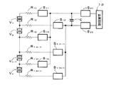
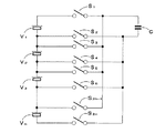
以下、第1実施例における本発明によるスイッチング回路及び電圧計測回路を、図面に基づいて説明する。図1は、本発明のスイッチング回路としてのフライングキャパシタ回路を組み込んだ電圧計測回路の一実施の形態を示す回路図である。同図に示すように、電圧計測回路は、2つのバッテリからなる単位セルV1〜Vnが複数直列に接続された組電池に対して、一つのコンデンサCを備えている。
First Embodiment Hereinafter, a switching circuit and a voltage measuring circuit according to the present invention in a first embodiment will be described with reference to the drawings. FIG. 1 is a circuit diagram showing an embodiment of a voltage measuring circuit incorporating a flying capacitor circuit as a switching circuit of the present invention. As shown in the figure, the voltage measuring circuit includes a single capacitor C for an assembled battery in which a plurality of unit cells V 1 to V n including two batteries are connected in series.
また、電圧計測回路は、上記単位セルV1〜Vnの各両端を上記コンデンサCの両端に順次接続するための複数の切替スイッチS11〜S1(n+1)と、この切替スイッチS11〜S1(n+1)と直列に接続された抵抗R11〜R1(n+1)とを備えている。切替スイッチS11〜S1(n+1)は、n個の単位セルV1〜Vnに対して、(n+1)個設けられている。上述した切替スイッチS11〜S1(n+1)及びコンデンサCがスイッチング回路を構成している。また、コンデンサCの両端は、計測スイッチS21及びS22を介して、コンデンサCの充電電圧を計測する計測回路10に接続されている。
Further, the voltage measuring circuit includes a plurality of changeover switches S 11 to
上述したフライングキャパシタ回路を組み込んだ電圧計測回路の動作について以下説明する。まず、図示しないロジック回路は、切替スイッチS11及びS12をオンして、単位セルV1の両端をコンデンサCの両端に接続する。これにより、コンデンサCの充電電圧は、単位セルV1の両端電圧に応じた値となる。次に、ロジック回路は、切替スイッチS11及びS12をオフにして、単位セルV1をコンデンサCから切り離すと共に、計測スイッチS21及びS22をオンして、計測回路10によりコンデンサCの充電電圧を計測させる。このコンデンサCの充電電圧を計測することにより、単位セルV1の両端電圧を計測することができる。
The operation of the voltage measuring circuit incorporating the above-described flying capacitor circuit will be described below. First, a logic circuit (not shown) turns on the changeover switches S 11 and S 12 to connect both ends of the unit cell V 1 to both ends of the capacitor C. Thereby, the charging voltage of the capacitor C becomes a value corresponding to the voltage across the unit cell V 1 . Next, the logic circuit turns off the switches S 11 and S 12 to disconnect the unit cell V 1 from the capacitor C, and turns on the measurement switches S 21 and S 22 to charge the capacitor C by the
さらにロジック回路は、切替スイッチS12及びS13をオンして、単位セルV2の両端をコンデンサCの両端に接続する。以下、ロジック回路は、上述したように切替スイッチS11〜S1(n+1)及び計測スイッチS21、S22のオンオフ制御する。そして、これにより単位セルV1〜Vnの両端を順次コンデンサCに接続させると共に、接続によって単位セルV1〜Vnの両端電圧に応じた値となったコンデンサCの充電電圧を計測回路10により計測させる。 Further, the logic circuit turns on the changeover switches S 12 and S 13 to connect both ends of the unit cell V 2 to both ends of the capacitor C. Hereinafter, the logic circuit performs on / off control of the changeover switches S 11 to S 1 (n + 1) and the measurement switches S 21 and S 22 as described above. As a result, both ends of the unit cells V 1 to V n are sequentially connected to the capacitor C, and the charging voltage of the capacitor C having a value corresponding to the voltage across the unit cells V 1 to V n by the connection is measured. Let me measure.
これらの動作から明らかなように、各単位セルV1〜Vn間に接続されている切替スイッチS12〜S1nは2つの単位セルV1〜Vnによって共用されている。具体的に述べると、例えば、単位セルV1のプラス側と、この単位セルV1のプラス側に接続されている単位セルV2のマイナス側とは、共通の切替スイッチS12を介してコンデンサCに接続されるようになっている。このため、各単位セルV1〜Vn間にある切替スイッチS12〜S1nには、双方向の電流が流れることとなる。 As apparent from these operations, the changeover switch S 12 to S 1n connected between the unit cells V 1 ~V n is shared by two unit cells V 1 ~V n. To be specific, for example, the plus side of the unit cell V 1, and the negative side of the unit cell V 2 which is connected to the positive side of the unit cell V 1 was, via a common changeover switch S 12 capacitor Connected to C. Therefore, the changeover switch S 12 to S 1n in between the unit cells V 1 ~V n, so that the bidirectional current flows.
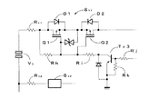
次に、上述した切替スイッチS11〜S1(n+1)の詳細な構成について図2及び図3を参照して説明する。図2は、切替スイッチS12〜S1(n+1)のうち任意の切替スイッチSmを示す回路図であり、図3は、最も高電圧となる単位セルV1のプラス側に接続されている切替スイッチS11を示す回路図である。 Next, the detailed configuration of the above-described changeover switches S 11 to S 1 (n + 1) will be described with reference to FIGS. Figure 2 is a circuit diagram showing an optional changeover switch S m of the changeover switch S 12 ~S 1 (n + 1 ), FIG. 3 is connected to the positive side of the unit cell V 1 to the highest voltage and a circuit diagram showing the changeover switch S 11 are.
まず、図2を参照して、切替スイッチS12〜S1(n+1)について説明する。同図に示すように、切替スイッチSmは、ソース−ドレイン方向が互いに逆向きになるように、直列に接続された2つの半導体スイッチとしてのNch.の電界効果トランジスタ(=FET)Q1及びQ2から構成されている。このため、各FETQ1及びQ2のソース−ドレイン間に発生する寄生ダイオードD1及びD2も、その順方向が互いに逆向きになる。 First, the changeover switches S 12 to S 1 (n + 1) will be described with reference to FIG. As shown in the figure, the changeover switch S m, the source - as drain direction is opposite to each other, Nch as two semiconductor switches connected in series. Field effect transistors (= FETs) Q1 and Q2. For this reason, the forward directions of the parasitic diodes D1 and D2 generated between the source and drain of the FETs Q1 and Q2 are opposite to each other.
上述したFETQ1及びQ2のゲートは、トランジスタTr1のコレクタ及び抵抗Rb間に接続されている。上記トランジスタTr1のエミッタは、抵抗Ra及びR1(m-1)を介して単位セルVm-1のプラス側に接続されると共に、抵抗Rcを介してベースと接続されている。一方、抵抗Rbは、単位セルVmのマイナス側に接続されている。 The gates of the FETs Q1 and Q2 described above are connected between the collector of the transistor Tr1 and the resistor Rb. The emitter of the transistor Tr1 is connected to the plus side of the unit cell V m−1 via resistors Ra and R 1 (m−1) , and is connected to the base via a resistor Rc. On the other hand, the resistance Rb is connected to the negative side of the unit cell V m.
また、トランジスタTr1のベースは、抵抗Rd及びReを介してトランジスタTr2のコレクタに接続される。このトランジスタTr2のエミッタはグランドに接続されている。一方、ベースは抵抗Rfを介して図示しないロジック回路に接続されるとともに、抵抗Rgを介してエミッタに接続されている。 The base of the transistor Tr1 is connected to the collector of the transistor Tr2 via the resistors Rd and Re. The emitter of this transistor Tr2 is connected to the ground. On the other hand, the base is connected to a logic circuit (not shown) via a resistor Rf, and is connected to an emitter via a resistor Rg.
これにより、5V系のロジック回路から5Vの制御信号がトランジスタTr2のベースに供給されると、トランジスタTr2がオンする。トランジスタTr2がオンすると抵抗R1(m-1)、Ra、Rc、Rd、Reの順に電流が流れる。このとき抵抗Rcに発生する電圧により、トランジスタTr1のエミッタ−ベース間にバイアスが与えられるため、トランジスタTr1もオンする。 Thus, when a 5V control signal is supplied from the 5V logic circuit to the base of the transistor Tr2, the transistor Tr2 is turned on. When the transistor Tr2 is turned on, a current flows in the order of the resistors R 1 (m−1) , Ra, Rc, Rd, and Re. At this time, the voltage generated in the resistor Rc applies a bias between the emitter and base of the transistor Tr1, so that the transistor Tr1 is also turned on.
トランジスタTr1がオンすると、FETQ1及びQ2のゲートには、単位セルVm及び単位セルVm-1の両端電圧の合計値を、抵抗R1(m-1)、Raと、抵抗Rbとで分圧した電圧が印加される。これにより、FETQ1及びQ2のゲートには、そのソースより高いバイアス電圧が印加され、FETQ1及びQ2はオンする。以上のことから明らかなように、抵抗Ra〜Rg及びトランジスタTr1、Tr2は5Vの制御信号をレベルシフトして、FETQ1及びQ2のゲートに印加するレベルシフト回路として働く。 When the transistor Tr1 is turned on, the total value of the voltage across the unit cell Vm and the unit cell Vm-1 is divided by the resistors R1 (m-1) , Ra and the resistor Rb at the gates of the FETs Q1 and Q2. A pressed voltage is applied. As a result, a bias voltage higher than that of the source is applied to the gates of the FETs Q1 and Q2, and the FETs Q1 and Q2 are turned on. As is apparent from the above, the resistors Ra to Rg and the transistors Tr1 and Tr2 function as a level shift circuit that shifts the level of the 5V control signal and applies it to the gates of the FETs Q1 and Q2.
次に、図3を参照して切替スイッチS11について説明する。同図に示すように、切替スイッチS11は、切替スイッチS12〜S1(n+1)と同様に、ソース−ドレイン方向が互いに逆向きになるように、直列接続された2つのPch.FETQ1及びQ2から構成されている。このため、各FETQ1及びQ2のソース−ドレイン間に発生する寄生ダイオードD1及びD2も、その順方向が逆向きになる。 Will now be described changeover switch S 11 with reference to FIG. As shown in the figure, the changeover switch S 11, like the changeover switch S 12 ~S 1 (n + 1 ), the source - as drain direction is opposite each other, two series-connected Pch. It consists of FETs Q1 and Q2. For this reason, the forward directions of the parasitic diodes D1 and D2 generated between the source and drain of the FETs Q1 and Q2 are reversed.
上述したFETQ1及びQ2のゲートは、抵抗Rhの一端と、抵抗Riの一端との間に接続されている。上記抵抗Rhの他端は、抵抗R11を介して単位セルV1に接続されている。一方、抵抗Riの他端は、トランジスタTr3のコレクタ−エミッタ間を介してグランドに接続されている。このトランジスタTr3のベースは抵抗Rjを介して図示しないロジック回路に接続されていると共に、抵抗Rkを介してエミッタに接続されている。 The gates of the FETs Q1 and Q2 described above are connected between one end of the resistor Rh and one end of the resistor Ri. The other end of the resistor Rh is connected to the unit cell V 1 through a resistor R 11 . On the other hand, the other end of the resistor Ri is connected to the ground via the collector-emitter of the transistor Tr3. The base of the transistor Tr3 is connected to a logic circuit (not shown) through a resistor Rj and is connected to the emitter through a resistor Rk.
これにより、5V系のロジック回路から5Vの制御信号がトランジスタTr3のベースに供給されると、トランジスタTr3がオンする。トランジスタTr3がオンすると、FETQ1及びQ2のゲートには、単位セルV1のプラス側の電圧を抵抗R11、抵抗Rhと、抵抗Riとで分圧した電圧が印加される。これにより、FETQ1及びQ2のゲートには、そのソースより低いバイアス電圧が印加され、FETQ1及びQ2がオンする。以上のことから明らかなように、抵抗Rh〜Rk及びトランジスタTr3は5Vの制御信号をレベルシフトして、FETQ1及びQ2のゲートに印加するレベルシフト回路として働く。 Thus, when a 5V control signal is supplied from the 5V logic circuit to the base of the transistor Tr3, the transistor Tr3 is turned on. When the transistor Tr3 is turned on, the gate of the FETQ1 and Q2, the positive side of the resistor voltage R 11 of the unit cell V 1, and the resistor Rh, divided voltage is applied by the resistance Ri. Thereby, a bias voltage lower than the source is applied to the gates of the FETs Q1 and Q2, and the FETs Q1 and Q2 are turned on. As is apparent from the above, the resistors Rh to Rk and the transistor Tr3 function as a level shift circuit that shifts the level of the 5V control signal and applies it to the gates of the FETs Q1 and Q2.
以上のフライングキャパシタ回路を組み込んだ電圧計測回路によれば、切替スイッチS11〜S1(n+1)は、ソース−ドレイン方向が互いに逆向きになるように、直列接続された2つのFETQ1及びQ2からそれぞれ構成されている。従って、切替スイッチS11〜S1(n+1)としてFETを用いれば双方向に電流を流すことができる。
According to the voltage measuring circuit incorporating the above flying capacitor circuit, the change-over switches S 11 to S 1 (n + 1) include two
しかも、ソース−ドレイン方向が互いに逆向きになるように、2つのFETQ1及びQ2を接続することにより、ソース−ドレイン方向に発生する寄生ダイオードD1及びD2の順方向が互いに逆向きとなる。これによりFETQ1及びQ2がオフのとき、寄生ダイオードD1及びD2を通じて、オン時における電流方向と逆方向に電流が流れてしまうことも防止することができ、切替スイッチとして、コスト、大きさ、耐久性、応答速度などが優れた半導体スイッチであるFETS11〜S1(n+1)を用いることができる。 Moreover, by connecting the two FETs Q1 and Q2 so that the source-drain directions are opposite to each other, the forward directions of the parasitic diodes D1 and D2 generated in the source-drain direction are opposite to each other. As a result, when the FETs Q1 and Q2 are off, it is possible to prevent the current from flowing in the direction opposite to the current direction when the FET is on through the parasitic diodes D1 and D2. FETS 11 to S 1 (n + 1) which are semiconductor switches having excellent response speed can be used.
また、上述した電圧計測回路によれば、レベルシフト回路により制御信号をレベルシフトしてFETQ1及びQ2のゲートに印加している。このレベルシフト回路により、5V系のロジック回路が出力する制御信号を用いて、高電圧にソースが接続されたFETQ1及びQ2のオンオフを制御することができ、高価なフォトMOSなどを用いる必要がなく、コストダウンを図ることができる。 Further, according to the voltage measurement circuit described above, the control signal is level-shifted by the level shift circuit and applied to the gates of the FETs Q1 and Q2. With this level shift circuit, it is possible to control on / off of FETs Q1 and Q2 whose sources are connected to a high voltage by using a control signal output from a 5V logic circuit, and there is no need to use an expensive photo MOS or the like. Cost reduction can be achieved.
ところで、切替スイッチS11のFETQ1及びQ2は最も高電圧である単位セルV1のプラス側に接続されているため、ゲートにソースより高い電圧を印加することができず、Nch.FETを用いることができない。そこで、上述した電圧計測回路のように、最も高電圧側にある単位セルV1のプラス側に接続されている切替スイッチS11が有するFETQ1及びQ2を高価なPch.FETとし、他の切替スイッチS12〜S1(n+1)はNch.FETとすれば、コストダウンを図ることができる。 Incidentally, since the FETQ1 and Q2 of the switch S 11 is connected to the positive side of the unit cell V 1 is the highest voltage, it is not possible to apply a higher source voltage to the gate, Nch. FET cannot be used. Therefore, as the voltage measuring circuit described above, the highest voltage side expensive Pch the FETQ1 and Q2 changeover switch S 11 has connected to the positive side of the unit cell V 1 in. The other change-over switches S 12 to S 1 (n + 1) are Nch. If the FET is used, the cost can be reduced.
さらに、上述したように、計測スイッチS21及びS22としてもFETQ1及びQ2を用いることにより、計測スイッチS21及びS22に双方向電流を流すことができる。しかも、切替スイッチS11〜S1(n+1)と同様に、ソース−ドレイン方向が互いに逆向きになるように、2つのFETQ1及びQ2を接続することにより、ソース−ドレイン方向に発生する寄生ダイオードD1及びD2の順方向が互いに逆向きとなる。これによりFETQ1及びQ2がオフであっても逆方向に電流が流れてしまうことも防止することができる。 Further, as described above, by using the FETQ1 and Q2 as measured switches S 21 and S 22, it is possible to flow a bidirectional current to the measurement switch S 21 and S 22. Moreover, as with the change-over switches S 11 to S 1 (n + 1) , parasitics generated in the source-drain direction by connecting the two FETs Q1 and Q2 so that the source-drain directions are opposite to each other. The forward directions of the diodes D1 and D2 are opposite to each other. As a result, even if the FETs Q1 and Q2 are off, it is possible to prevent current from flowing in the reverse direction.
なお、上述した実施の形態では、切替スイッチS11及びS1(n+1)についても、ソース−ドレイン方向が互いに逆向きとなるように直列接続した2つのFETQ1及びQ2を用いていた。しかしながら、切替スイッチS11及びS1(n+1)には、単方向の電流しか流れないため、トランジスタなどの単方向スイッチを用いることも考えられる。 In the embodiment described above, for the changeover switches S 11 and S 1 (n + 1), the source - drain direction were using two FETQ1 and Q2 connected in series so as to be opposite to each other. However, the changeover switch S 11 and S1 (n + 1), since only flow unidirectional current, it is considered to use a unidirectional switch such as a transistor.
第2実施例
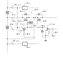
次に、第2実施例における本発明によるスイッチング回路及び電圧計測回路を、図面に基づいて説明する。図4は、本発明のスイッチング回路としてのフライングキャパシタ回路を組み込んだ電圧計測回路の一実施の形態を示す回路図である。なお、同図において、図1〜図3について上述した第1実施例と同等の部分には同一符号を付して詳細な説明を省略する。
Second Embodiment Next, a switching circuit and a voltage measuring circuit according to the present invention in a second embodiment will be described with reference to the drawings. FIG. 4 is a circuit diagram showing an embodiment of a voltage measuring circuit incorporating a flying capacitor circuit as a switching circuit of the present invention. In the figure, the same parts as those in the first embodiment described above with reference to FIGS.
第1実施例と異なる点は、切替スイッチS11〜S1(n+1)のドライブ回路である。第1実施例では、組電池の電圧を分圧して切替スイッチS11〜S1(n+1)を構成するFETQ1、Q2のゲート電圧を得ていたが、第2実施形態では以下のように構成している。図4に示すように、FETQ1、Q2のドライブ回路は、このFETQ1及びQ2のゲート−ソース間に設けられた抵抗Rdr(=抵抗素子)と、この抵抗Rdrの両端に設けられたコンデンサCr1及びCr2(=ドライブ用コンデンサ)と、コンデンサCr1及びCr2を介して抵抗Rdrの両端に交流電圧を印加する発振回路20とを備えている。
The difference from the first embodiment is the drive circuit of the changeover switches S 11 to S 1 (n + 1) . In the first embodiment, it had gained the gate voltage of FET Q1, Q2 constituting the selector switch S 11 ~S 1 (n + 1 ) the voltage of the assembled battery divides, in the second embodiment as follows It is composed. As shown in FIG. 4, the drive circuit of the FETs Q1 and Q2 includes a resistor Rdr (= resistive element) provided between the gate and source of the FETs Q1 and Q2, and capacitors Cr1 and Cr2 provided at both ends of the resistor Rdr. (= Capacitor for driving) and an
また、ドライブ回路は、発振回路20とコンデンサCr2との間に設けたドライブ用スイッチSWと、このドライブ用スイッチSWのオンオフを指示する制御信号を出力するロジック回路30とを備えている。
Further, the drive circuit includes a drive switch SW provided between the
上述した構成の電圧計測装置のドライブ回路の動作を以下説明する。上述した発振回路20は、常時発振して、交流電圧を出力している。今、ロジック回路30がドライブ用スイッチSWに制御信号を出力すると、ドライブ用スイッチSWがオンして、抵抗Rdrの両端に発振回路20からの交流電圧が印加される。これによりFETQ1及びQ2のソース−ゲート間にバイアスがかかり2つのFETQ1及びQ2をオンすることができる。一方、ロジック回路30がドライブ用スイッチSWに対する制御信号の出力を停止すると、ドライブ用スイッチSWがオフして、交流電圧の供給経路が断たれるため、FETQ1及びQ2がオフする。
The operation of the drive circuit of the voltage measuring apparatus having the above configuration will be described below. The
以上の構成によれば、コンデンサCr1及びCr2により発振回路20と組電池とは直流的に絶縁することができるため、発振回路20や、ロジック回路30は組電池とは異なる例えば5V系の低電圧源を電源とすることができる。このため、例えば、発振回路20とコンデンサCr2との間に設けたドライブ用スイッチSWも高耐圧が不要であり、安全な装置を安価に得ることができる。
According to the above configuration, since the
また、抵抗Rdrに印加する交流電圧をオンオフするドライブ用スイッチSWと、このドライブ用スイッチSWを制御するロジック回路30とを設けることにより、複数の切替スイッチS11〜S1(n+1)に対して発振回路20を一つにすることができ、各切替スイッチS11〜S1(n+1)に対して各々発振回路20を設ける必要がない。このため、構成が簡単となり、コストダウンを図ることができる。
Further, by providing a drive switch SW for turning on and off the AC voltage applied to the resistor Rdr and a
なお、第2実施例としては、さらに、抵抗Rdrと並列にコンデンサを設けることも考えられる。このような構成にすることにより、抵抗Rdrとコンデンサとがフィルタとして働き、ノイズなどによって不用意にFETQ1及びQ2がオンしてしまうことを防ぐことができる。 In the second embodiment, a capacitor may be provided in parallel with the resistor Rdr. With such a configuration, the resistor Rdr and the capacitor function as a filter, and it is possible to prevent the FETs Q1 and Q2 from being inadvertently turned on due to noise or the like.
C コンデンサ
Cr1、Cr2 ドライブ用コンデンサ
S11〜S1(n+1) 切替スイッチ
S21、S22 計測スイッチ
S211〜S21n 計測スイッチ
S221〜S22n 計測スイッチ
SW ドライブ用スイッチ
V1〜Vn 単位セル
Q1、Q2 電界効果トランジスタ(半導体スイッチ)
Rdr 抵抗素子
20 発振回路
30 ロジック回路
C capacitor Cr1, Cr2 drive capacitor S 11 ~S 1 (n + 1 ) change-over switch S 21, S 22 Measurement switch S 211 to S 21n measuring switch S 221 to S 22n measurement switch SW Drive switch V 1 ~V n Unit cell Q1, Q2 Field effect transistor (semiconductor switch)
Claims (7)
前記切替スイッチは、ソース−ドレイン方向が互いに逆向きになるように、直列接続された2つの半導体スイッチを有することを特徴とするスイッチング回路。 In a switching circuit comprising a capacitor and a plurality of changeover switches for sequentially connecting both ends of each unit cell of an assembled battery configured by connecting a plurality of unit cells made of a battery in series,
The switching switch includes two semiconductor switches connected in series so that the source-drain directions are opposite to each other.
一の前記単位セルのマイナス側と、当該単位セルのマイナス側に接続されている二の前記単位セルのプラス側とは、共通の前記切替スイッチを介して前記コンデンサに接続されていることを特徴とするスイッチング回路。 The switching circuit according to claim 1,
The negative side of one unit cell and the positive side of the second unit cell connected to the negative side of the unit cell are connected to the capacitor via the common changeover switch. Switching circuit.
前記半導体スイッチのオンオフを指示する制御信号を出力するロジック回路と、
前記制御信号をレベルシフトして、前記半導体スイッチのゲートに出力するレベルシフト回路とをさらに備えたことを特徴とするスイッチング回路。 The switching circuit according to claim 1 or 2,
A logic circuit that outputs a control signal instructing on / off of the semiconductor switch;
A switching circuit further comprising: a level shift circuit that shifts the level of the control signal and outputs the level to the gate of the semiconductor switch.
前記半導体スイッチのソース−ゲート間に設けた抵抗素子と、
該抵抗素子の両端に接続したドライブ用コンデンサと、
前記ドライブ用コンデンサを介して前記抵抗素子の両端に交流電圧を印加する発振回路とを備えたことを特徴とするスイッチング回路。 The switching circuit according to claim 1 or 2,
A resistance element provided between a source and a gate of the semiconductor switch;
A drive capacitor connected to both ends of the resistance element;
A switching circuit comprising: an oscillation circuit that applies an AC voltage to both ends of the resistance element via the drive capacitor.
前記発振回路と前記ドライブ用コンデンサとの間に設けたドライブ用スイッチと、
前記ドライブ用スイッチのオンオフを指示する制御信号を出力するロジック回路とを備えたことを特徴とするスイッチング回路。 A switching circuit according to claim 4, wherein
A drive switch provided between the oscillation circuit and the drive capacitor;
A switching circuit comprising: a logic circuit that outputs a control signal instructing on / off of the drive switch.
前記切替スイッチのうち、最も高圧側にある前記単位セルのプラス側に接続されている半導体スイッチはPch.であり、他の半導体スイッチはNch.であることを特徴とするスイッチング回路。 A switching circuit according to any one of claims 1 to 5,
Of the changeover switches, the semiconductor switch connected to the positive side of the unit cell on the highest voltage side is Pch. The other semiconductor switches are Nch. A switching circuit characterized by
前記コンデンサの両端電圧を計測する電圧計測手段と、
前記コンデンサの両端と前記電圧計測手段との間に設けられた計測スイッチとをさらに備え、
前記計測スイッチは、ソース−ドレイン方向が互いに逆向きになるように、直列接続された2つの半導体スイッチを有することを特徴とする電圧計測回路。 A switching circuit according to any one of claims 1 to 6,
Voltage measuring means for measuring the voltage across the capacitor;
A measuring switch provided between both ends of the capacitor and the voltage measuring means;
The voltage measurement circuit according to claim 1, wherein the measurement switch includes two semiconductor switches connected in series so that the source-drain directions are opposite to each other.
Priority Applications (3)
| Application Number | Priority Date | Filing Date | Title |
|---|---|---|---|
| JP2004167135A JP4351585B2 (en) | 2003-06-06 | 2004-06-04 | Switching circuit and voltage measurement circuit |
| US11/002,236 US7719283B2 (en) | 2004-06-04 | 2004-12-03 | Switching circuit and voltage measuring circuit |
| CNB2004100978307A CN1312842C (en) | 2004-06-04 | 2004-12-03 | Switching circuit and voltage measuring circuit |
Applications Claiming Priority (2)
| Application Number | Priority Date | Filing Date | Title |
|---|---|---|---|
| JP2003162126 | 2003-06-06 | ||
| JP2004167135A JP4351585B2 (en) | 2003-06-06 | 2004-06-04 | Switching circuit and voltage measurement circuit |
Publications (2)
| Publication Number | Publication Date |
|---|---|
| JP2005017289A true JP2005017289A (en) | 2005-01-20 |
| JP4351585B2 JP4351585B2 (en) | 2009-10-28 |
Family
ID=34196835
Family Applications (1)
| Application Number | Title | Priority Date | Filing Date |
|---|---|---|---|
| JP2004167135A Expired - Fee Related JP4351585B2 (en) | 2003-06-06 | 2004-06-04 | Switching circuit and voltage measurement circuit |
Country Status (1)
| Country | Link |
|---|---|
| JP (1) | JP4351585B2 (en) |
Cited By (10)
| Publication number | Priority date | Publication date | Assignee | Title |
|---|---|---|---|---|
| JP2010515883A (en) * | 2007-01-07 | 2010-05-13 | エナーデル、インク | Method and system for series connected cell voltage measurement using flying capacitors |
| WO2012144373A1 (en) | 2011-04-21 | 2012-10-26 | ルネサスエレクトロニクス株式会社 | Switch circuit, selection circuit, and voltage measurement device |
| JP2013066369A (en) * | 2011-08-31 | 2013-04-11 | Sony Corp | Switch, charge monitoring apparatus and rechargeable battery module |
| US9397266B2 (en) | 2007-11-14 | 2016-07-19 | Cree, Inc. | Lateral semiconductor light emitting diodes having large area contacts |
| US9484499B2 (en) | 2007-04-20 | 2016-11-01 | Cree, Inc. | Transparent ohmic contacts on light emitting diodes with carrier substrates |
| USD826871S1 (en) | 2014-12-11 | 2018-08-28 | Cree, Inc. | Light emitting diode device |
| CN112363037A (en) * | 2019-07-25 | 2021-02-12 | 华润微电子(重庆)有限公司 | Limit performance verification circuit, system and method for field effect transistor |
| EP3934099A1 (en) * | 2020-07-01 | 2022-01-05 | NXP USA, Inc. | A switch |
| US11342600B2 (en) | 2020-07-01 | 2022-05-24 | Nxp Usa, Inc. | Switch |
| CN115664378A (en) * | 2022-11-15 | 2023-01-31 | 青岛鼎信通讯股份有限公司 | Resonance switching circuit and medium-voltage power communication system |
-
2004
- 2004-06-04 JP JP2004167135A patent/JP4351585B2/en not_active Expired - Fee Related
Cited By (13)
| Publication number | Priority date | Publication date | Assignee | Title |
|---|---|---|---|---|
| JP2010515883A (en) * | 2007-01-07 | 2010-05-13 | エナーデル、インク | Method and system for series connected cell voltage measurement using flying capacitors |
| US9484499B2 (en) | 2007-04-20 | 2016-11-01 | Cree, Inc. | Transparent ohmic contacts on light emitting diodes with carrier substrates |
| US9397266B2 (en) | 2007-11-14 | 2016-07-19 | Cree, Inc. | Lateral semiconductor light emitting diodes having large area contacts |
| WO2012144373A1 (en) | 2011-04-21 | 2012-10-26 | ルネサスエレクトロニクス株式会社 | Switch circuit, selection circuit, and voltage measurement device |
| US9453886B2 (en) | 2011-04-21 | 2016-09-27 | Renesas Electronics Corporation | Switch circuit, selection circuit, and voltage measurement device |
| JP2013066369A (en) * | 2011-08-31 | 2013-04-11 | Sony Corp | Switch, charge monitoring apparatus and rechargeable battery module |
| USD826871S1 (en) | 2014-12-11 | 2018-08-28 | Cree, Inc. | Light emitting diode device |
| CN112363037A (en) * | 2019-07-25 | 2021-02-12 | 华润微电子(重庆)有限公司 | Limit performance verification circuit, system and method for field effect transistor |
| CN112363037B (en) * | 2019-07-25 | 2024-03-01 | 华润微电子(重庆)有限公司 | Field effect transistor limit performance verification circuit, system and method |
| EP3934099A1 (en) * | 2020-07-01 | 2022-01-05 | NXP USA, Inc. | A switch |
| US11342600B2 (en) | 2020-07-01 | 2022-05-24 | Nxp Usa, Inc. | Switch |
| US11394383B2 (en) | 2020-07-01 | 2022-07-19 | Nxp Usa, Inc. | Switch |
| CN115664378A (en) * | 2022-11-15 | 2023-01-31 | 青岛鼎信通讯股份有限公司 | Resonance switching circuit and medium-voltage power communication system |
Also Published As
| Publication number | Publication date |
|---|---|
| JP4351585B2 (en) | 2009-10-28 |
Similar Documents
| Publication | Publication Date | Title |
|---|---|---|
| JP4351585B2 (en) | Switching circuit and voltage measurement circuit | |
| JP4536108B2 (en) | Load drive circuit | |
| US9954519B2 (en) | Electronic switch, and corresponding device and method | |
| JP2011223309A (en) | Load drive circuit with bidirectional current detection function | |
| JP2000217262A (en) | Programmable battery power drop detector | |
| JP4983377B2 (en) | Voltage detector for storage element | |
| JP4256807B2 (en) | Switching circuit and individual voltage measuring device | |
| JP5710175B2 (en) | Power switching circuit | |
| JP4199578B2 (en) | Voltage detection circuit | |
| US7719283B2 (en) | Switching circuit and voltage measuring circuit | |
| JP5961944B2 (en) | Gate drive circuit | |
| JP4177216B2 (en) | Switching circuit and voltage measurement circuit | |
| JP5348115B2 (en) | Load drive device | |
| JP2560710B2 (en) | Integrated switching circuit | |
| JP6119413B2 (en) | Semiconductor circuit and voltage measurement system | |
| JP3632305B2 (en) | Motor drive device | |
| JP2002111463A (en) | Fet driving circuit and switching device | |
| US7495401B2 (en) | Control systems and switch devices thereof | |
| JP2006020414A (en) | Power supply device | |
| KR200198482Y1 (en) | A normal and reverse driving circuit of multi-motor which saves the switching element | |
| JP3566240B2 (en) | High voltage output control circuit | |
| JP4640680B2 (en) | Method and circuit for driving transistor bridge | |
| JP2549707B2 (en) | Switch driver | |
| JP2016184815A (en) | Gate driver | |
| JP2004248453A (en) | Charge pumping circuit |
Legal Events
| Date | Code | Title | Description |
|---|---|---|---|
| A621 | Written request for application examination |
Free format text: JAPANESE INTERMEDIATE CODE: A621 Effective date: 20061024 |
|
| A977 | Report on retrieval |
Free format text: JAPANESE INTERMEDIATE CODE: A971007 Effective date: 20090424 |
|
| A131 | Notification of reasons for refusal |
Free format text: JAPANESE INTERMEDIATE CODE: A131 Effective date: 20090428 |
|
| A521 | Request for written amendment filed |
Free format text: JAPANESE INTERMEDIATE CODE: A523 Effective date: 20090625 |
|
| TRDD | Decision of grant or rejection written | ||
| A01 | Written decision to grant a patent or to grant a registration (utility model) |
Free format text: JAPANESE INTERMEDIATE CODE: A01 Effective date: 20090714 |
|
| A01 | Written decision to grant a patent or to grant a registration (utility model) |
Free format text: JAPANESE INTERMEDIATE CODE: A01 |
|
| A61 | First payment of annual fees (during grant procedure) |
Free format text: JAPANESE INTERMEDIATE CODE: A61 Effective date: 20090724 |
|
| FPAY | Renewal fee payment (event date is renewal date of database) |
Free format text: PAYMENT UNTIL: 20120731 Year of fee payment: 3 |
|
| R150 | Certificate of patent or registration of utility model |
Ref document number: 4351585 Country of ref document: JP Free format text: JAPANESE INTERMEDIATE CODE: R150 Free format text: JAPANESE INTERMEDIATE CODE: R150 |
|
| FPAY | Renewal fee payment (event date is renewal date of database) |
Free format text: PAYMENT UNTIL: 20130731 Year of fee payment: 4 |
|
| R250 | Receipt of annual fees |
Free format text: JAPANESE INTERMEDIATE CODE: R250 |
|
| R250 | Receipt of annual fees |
Free format text: JAPANESE INTERMEDIATE CODE: R250 |
|
| R250 | Receipt of annual fees |
Free format text: JAPANESE INTERMEDIATE CODE: R250 |
|
| R250 | Receipt of annual fees |
Free format text: JAPANESE INTERMEDIATE CODE: R250 |
|
| R250 | Receipt of annual fees |
Free format text: JAPANESE INTERMEDIATE CODE: R250 |
|
| LAPS | Cancellation because of no payment of annual fees |