JP2004536543A - Isolated drive circuit used in switch mode power converter - Google Patents
Isolated drive circuit used in switch mode power converter Download PDFInfo
- Publication number
- JP2004536543A JP2004536543A JP2002561354A JP2002561354A JP2004536543A JP 2004536543 A JP2004536543 A JP 2004536543A JP 2002561354 A JP2002561354 A JP 2002561354A JP 2002561354 A JP2002561354 A JP 2002561354A JP 2004536543 A JP2004536543 A JP 2004536543A
- Authority
- JP
- Japan
- Prior art keywords
- primary
- switch
- power
- power converter
- input
- Prior art date
- Legal status (The legal status is an assumption and is not a legal conclusion. Google has not performed a legal analysis and makes no representation as to the accuracy of the status listed.)
- Pending
Links
Images


Classifications
-
- H—ELECTRICITY
- H02—GENERATION; CONVERSION OR DISTRIBUTION OF ELECTRIC POWER
- H02M—APPARATUS FOR CONVERSION BETWEEN AC AND AC, BETWEEN AC AND DC, OR BETWEEN DC AND DC, AND FOR USE WITH MAINS OR SIMILAR POWER SUPPLY SYSTEMS; CONVERSION OF DC OR AC INPUT POWER INTO SURGE OUTPUT POWER; CONTROL OR REGULATION THEREOF
- H02M1/00—Details of apparatus for conversion
- H02M1/08—Circuits specially adapted for the generation of control voltages for semiconductor devices incorporated in static converters
- H02M1/088—Circuits specially adapted for the generation of control voltages for semiconductor devices incorporated in static converters for the simultaneous control of series or parallel connected semiconductor devices
-
- H—ELECTRICITY
- H02—GENERATION; CONVERSION OR DISTRIBUTION OF ELECTRIC POWER
- H02M—APPARATUS FOR CONVERSION BETWEEN AC AND AC, BETWEEN AC AND DC, OR BETWEEN DC AND DC, AND FOR USE WITH MAINS OR SIMILAR POWER SUPPLY SYSTEMS; CONVERSION OF DC OR AC INPUT POWER INTO SURGE OUTPUT POWER; CONTROL OR REGULATION THEREOF
- H02M1/00—Details of apparatus for conversion
- H02M1/38—Means for preventing simultaneous conduction of switches
Landscapes
- Engineering & Computer Science (AREA)
- Power Engineering (AREA)
- Dc-Dc Converters (AREA)
- Power Conversion In General (AREA)
- Control Of Motors That Do Not Use Commutators (AREA)
- Cookers (AREA)
Abstract
Description
【技術分野】
【0001】
本発明は、一般に、スイッチモード電力コンバータに関するものであり、より具体的には、絶縁機能および同期整流を用いたフルブリッジ・トポロジで高い性能を示す単純な駆動回路とイネーブル機能を提供する。
【背景技術】
【0002】
スイッチモード電力コンバータは、インダクタ、トランス、またはキャパシタ、または何らかの組み合わせをエネルギー貯蔵要素として使用し、入力源から出力負荷へ離散パルスでエネルギーを伝達する回路である。回路の負荷限界内に定電圧を維持するため他の回路を追加する。入力電圧に関して出力電圧をステップアップ(ブースト)、ステップダウン(バック)、または反転するように基本回路を構成することができる。トランスを使用することで、出力電圧を入力電圧から電気的に絶縁することができる。
【0003】
スイッチモード・コンバータは過去15年の間にごくわずかしか変わっておらず、ほとんどショットキー・ダイオードを使用して出力を整流している。しかし、業界ではDC/DC電源設計者に対して、デジタル回路に必要な電圧をさらに引き下げ、周波数を高めるという新しい課題を突きつけている。整流にショットキー・ダイオードを使用したコンバータでは出力電圧に関して大きな順電圧降下が発生するため、その効率は一般に比較的低い。効率が低ければ、熱の散逸が大きくなるため、ヒート・シンクを使用してこれを除去する必要があるが、スペースを取る。このショットキー・ダイオードをMOSFETトランジスタで実際に実現されている「同期整流器」で置き換えることにより、コンバータの効率を劇的に向上させることができる。同期整流器は、新しいものではないが、以前には主に「オン」抵抗が高いせいで高価すぎ受け入れられることはなかった。しかし、コストが下がり、性能が向上するにつれ、同期整流器はたちまち、特に低電圧コンバータ用の有望なコンポーネントとなった。
【0004】
さまざまなコンバータ・トポロジで自己駆動同期整流器を使用することは非常に魅力的かつポピュラーであるが、それは駆動信号の間に絶縁を追加する必要がないからである。簡素化という利点がある。しかし、同期整流器と一次側スイッチの間に短絡が生じるだけでなく、同期整流に使用されるMOSFETの寄生アンチパラレル・ダイオードの逆回復電流も生じるという欠点がある。これらの貫通電流を最小限に抑えるために、通常、インダクタンス(または可飽和インダクタ)が同期整流器と直列に入れられる。これは、スイッチング周波数が例えば100kHz〜200kHzと低い場合の解決方法であるが、スイッチング周波数が高くなると(200kHz以上)ふさわしくない。特にスイッチング周波数が300〜400kHzだと、これは最適な解決方法とはいえない。これは、同期整流器と直列に入れられているインダクタンスが大きいと、二次電流のdi/dtが低速になることにより電源トランスの二次側の実効デューティ・サイクルが低下するためである。その結果、電源トランスに大きな電圧ヘッドルームが必要になるが、これは実効巻数比が小さくなり、効率が低下することを意味する。
【0005】
自己駆動同期整流が高いスイッチング周波数に適していないもう1つの理由は、同期整流器(MOSFET)のボディ・ダイオード内の逆回復電流の発生と、一次側スイッチ(通常はMOSFET)内のターンオン電流の増大による潜在的損失である。
【0006】
自己駆動同期整流器が好ましい解決方法でなかった3番目の理由は、電源トランスから引き出される駆動電圧が入力電圧に左右され、したがって著しく変動する可能性がある(200%〜300%)という点である。その結果、駆動回路の電力消費量が入力電圧に従い指数関数的に変化し、なおいっそう変動が大きくなり(400%〜900%)、コンバータ全体の効率が低下する可能性がある。
【0007】
さらに好ましい解決方法では、直接駆動を用いて同期整流器に電力を供給し、メイン・スイッチの駆動信号(一次側)と同期整流器(二次側)とのタイミングを適切に制御する。したがって、この解決方法では、スイッチング周波数が高い場合であっても同期整流器の動作を非常に効率的なものとすることができる。直接駆動同期整流器の他の利点として、さらに、駆動電圧(ゲート−ソース間)が一定であり、入力電圧に関係せず、このため広い入力電圧範囲にわたって効率を高められるという点が挙げられる。
【0008】
短絡(ショートを引き起こす同時導通)を避けるため一次側スイッチの駆動信号と二次側スイッチの駆動信号の間に遅延を設定する必要がある。電力コンバータが低いスイッチング周波数(例えば、100kHz)で動作している場合、スイッチング期間に関する短絡が発生する期間の割合が小さい(通常、40ns/10μs)ためスイッチの短絡は許容できる。また、低い周波数で動作する設計のトランスであれば、漏れインダクタンスが大きくなり、短絡電流が減少する。スイッチング周波数が高い場合(100kHz超)、短絡はさらに許容できないものとなる(500kHzスイッチング周波数に対して40ns/2μs)。また、スイッチング周波数が高い場合、効率を高めるためには、トランス内の漏れインダクタンスだけでなく電力段全体の漏れインダクタンスも最小限に抑えなければならない。したがって、短絡時間による電流が無視できないくらいの大きさになり、コンバータ全体の効率が低下し、電力コンポーネントの発熱が著しく増大する可能性がある。
【発明の開示】
【発明が解決しようとする課題】
【0009】
本発明は、フルブリッジ・トポロジによりスイッチモード電力コンバータ内の一次側スイッチおよび同期整流器に適切な遅延を生じさせるための駆動トランスおよび関連する回路を提供しようとするものである。
【課題を解決するための手段】
【0010】
本発明の一実施形態では、1つの駆動トランスを使用して、適切な遅延を与えるだけでなく、フルブリッジ・トポロジ内の一次側スイッチ、特に高電圧側スイッチを駆動するための電力を供給する。駆動トランスの漏れインダクタンスを使用して、ターンオフに著しい遅延がない間にメイン・スイッチ(一次側)のターンオンを遅延させる。駆動トランスの巻線の数は、制御回路がコンバータの出力を基準にしているときには最小4に、制御回路がコンバータの入力を基準にしているときには最小5にする。フルブリッジ・コンバータでは、制御回路はコンバータの出力を基準としており、4つの巻線は、(1)出力を基準とし、同期整流器を駆動するのに適切な波形を供給する制御および駆動回路(例えば、パルス幅変調(PWM)型)信号、(2)2つの底部一次側スイッチの駆動、(3)1つの上部一次側スイッチの駆動、(4)第2の上部一次側スイッチの駆動用である。制御回路がコンバータの入力を基準としている場合、5つの巻線があり、(1)コンバータの入力を基準とする制御および駆動回路信号、(2)同期整流器を駆動するための適切な波形の供給、(3)1つの上部一次側スイッチの駆動、(4)第2の上部一次側スイッチの駆動、および(5)2つの底部一次側スイッチの駆動用である。本発明の他の目的は、コンバータの入力または出力側のいずれかに配置されているコントローラまたは保護回路を介して入力または出力側のいずれかで感知された状態によりモジュールをイネーブル/ディセーブルする手段を提供することである。
【0011】
本発明の他の目的、利点、および特徴は、以下の詳細な説明を付属の図面とともに読むとより明確に理解できるであろう。
【発明を実施するための最良の形態】
【0012】
図1Aおよび1Bは、本発明の一実施形態による絶縁駆動回路を使用した同期整流器を採用するフルブリッジ・トポロジを示している。4つの一次側スイッチ(トランジスタ)Q10、Q20、Q30、およびQ40、電源トランスT2、同期整流器S1およびS2、出力インダクタL0、およびキャパシタC0は、フルブリッジ・コンバータの電力段を形成する。スイッチQ10およびQ20は、ブリッジの一方の脚を形成し、スイッチQ30およびQ40はブリッジの他方の脚を形成する。ブリッジの両方の脚は、入力電圧間に接続され、Q10とQ40は正側に接続され、Q20とQ30は負側に接続される。同じ脚(Q10とQ20、およびQ30とQ40)内のスイッチは常に、位相がずれた状態で導通し、対角線のスイッチは同時に導通する(Q10とQ30、およびQ20とQ40)。電源トランスT2の一次巻線Npは、2つの脚の間の中点に接続されている。2つの二次側巻線NS1およびNS2は同じであるのが好ましく、直列に接続されている。2つの巻線NS1およびNS2の間の共通点が出力インダクタL0の一端に接続されている。インダクタの第2の端は、出力キャパシタC0に接続されている。巻線NS1の第2の端は、同期整流器S1に接続され、巻線NS2の第2の端は、同期整流器S2に接続されている。基本的なフルブリッジ・コンバータでは、巻線の極性を選択する基準は(a)スイッチQ10およびQ30がオンになっているとき、S1はオン、S2はオフであり、(b)スイッチQ20およびQ40がオンのとき、同期整流器S2はオン、同期整流器S1はオフであり、(c)4つの一次側スイッチQ10、Q20、Q30、Q40がすべてオフのとき、S1とS2は両方ともオンで、電源トランスT2の3つすべての巻線が短絡しているという条件である。
【0013】
図1Bに示されているように、出力電圧VOUTをブロック100内の基準電圧VRと比較する(基準電圧VRおよび補償ネットワークがある誤差増幅器を備える)。ブロック100の出力が絶縁回路101(通常、オプトカプラまたは絶縁トランス)に供給され、誤差信号VEが例えば、PWMコントローラ、位相外れ出力OUTAおよびOUTBを発生する2つのドライバ段、およびON/OFFロジックを備えるがこれに限定されないコントローラ・ブロック102に供給される。ブロック102は、さらに、コンバータによくありがちな追加保護機能を備えることもできる。ただし、これらはこの説明の目的には関連がないため、省いている。ドライバ出力OUTAおよびOUTBは、2つの一次側スイッチを同時に駆動できる(Q10とQ30、およびQ20とQ40)だけでなく、磁化電流を駆動トランスT1に供給することもできる。図1Aでは、コントローラおよびドライバOUTAとOUTBは−VINを基準としており、したがってコンバータの入力を基準とすることに留意されたい。
【0014】
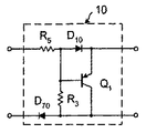
駆動トランスT1には5つの巻線N1〜N5がある(図1A)。その漏れインダクタンスが外部インダクタンスL1、L2、L3、L4、およびL5として図1Aに明示的に示されている。巻線N5は、信号OUTAおよびOUTBでブロック102から駆動される。キャパシタC1は、直流ブロッキング・キャパシタとして使用される。巻線N1は、一端がトランジスタQ10のソースに接続され、第2の端が直列ダイオードD10と抵抗器R5を介してトランジスタQ10のゲートに接続されている。抵抗器R5は、ダイオードD10と直列に接続されており、漏れインダクタンスL1とトランジスタQ10の入力容量の間の共振により生じるQ10のゲート上の発振を減衰させる。トランジスタQ1は、pチャネルMOSFETとして図に示されているが、Q10のゲートとソースの間に接続されており、そのゲートは抵抗器R3経由で、点極性でマークされている巻線N1の端に接続されている。抵抗器R10は、トランジスタQ10のゲートおよびソース間に接続されており、これを使用して、巻線N1間の電圧が0になったときのQ10の雑音排除性を高める。抵抗器R3は、トランジスタQ1のゲートと直列に接続されており、トランジスタQ1の入力容量と巻線N1の漏れインダクタンスL1との間に生じる望ましくない発振を減衰させる。
【0015】
同様に、巻線N2は、一端がトランジスタQ40のソースに接続され、第2の端が直列ダイオードD40と抵抗器R41を介してトランジスタQ40のゲートに接続されている。抵抗器R41は、ダイオードD40と直列に接続されており、漏れインダクタンスL2とトランジスタQ40の入力容量との間の共振で生じるトランジスタQ40のゲート上の発振を減衰させる。トランジスタQ4は、pチャネルMOSFETとして図に示されているが、トランジスタQ40のゲートとソースの間に接続されており、そのゲートは抵抗器R9経由で、点マークなしで巻線N2の端に接続されている。抵抗器R40は、トランジスタQ40のゲートおよびソース間に接続されており、これを使用して、巻線N2間の電圧が0になったときのQ40の雑音排除性を高める。抵抗器R9は、トランジスタQ4のゲートと直列に接続されており、トランジスタQ4の入力容量と巻線N2の漏れインダクタンスL2との間に生じる望ましくない発振を減衰させる。
【0016】
巻線N4を使用して、入力電圧(−VIN)の負側に接続されている2つの底部一次側スイッチQ20とQ30を駆動する。巻線N4の各端は、ダイオードD50およびダイオードD60とともに−VINに接続されている。点極性でマークされている(さらに図1Aで点「A」としてマークされてもいる)巻線N4の端が、ダイオードD30および抵抗器R8との直列接続により、トランジスタQ30のゲートに接続されている。トランジスタQ3は、pチャネルMOSFETとして図に示されているが、トランジスタQ30のゲートとソースの間に接続されており、そのゲートは抵抗器R7経由で、巻線N4の端「A」に接続されている。抵抗器R8は、ダイオードD30と直列に接続されており、漏れインダクタンスL4と一次側スイッチQ30の入力容量との間の共振で生じるトランジスタQ30のゲート上の発振を減衰させる。抵抗器R30は、トランジスタQ30のゲートおよびソース間に接続されており、これを使用して、巻線N4間の電圧が0になったときのQ30の雑音排除性を高める。抵抗器R7は、Q3のゲートと直列に接続されており、Q3の入力容量と巻線N4の漏れインダクタンスL4との間に生じる望ましくない発振を減衰させる。抵抗器R60は、巻線N4の電圧が0のときにゲートをドレインに接続することによりQ3をオフ状態に保持するために接続されている。
【0017】
点極性でマークされていない(さらに図1Aで点「B」としてマークされてもいる)巻線N4の端が、ダイオードD20および抵抗器R6との直列接続によりトランジスタQ20のゲートに接続されている。抵抗器R6は、ダイオードD20と直列に接続されており、漏れインダクタンスL4と一次側スイッチQ20の入力容量との間の共振で生じるトランジスタQ20のゲート上の発振を減衰させる。トランジスタQ2は、pチャネルMOSFETとして図に示されているが、トランジスタQ20のゲートとソースの間に接続されており、そのゲートは抵抗器R4経由で、巻線N4の端「B」に接続されている。抵抗器R20は、トランジスタQ20のゲートおよびソース間に接続されており、これを使用して、巻線N4間の電圧が0になったときのQ20の雑音排除性を高める。抵抗器R4は、トランジスタQ2のゲートと直列に接続されており、Q2の入力容量と巻線N4の漏れインダクタンスL4との間に生じる望ましくない発振を減衰させる。抵抗器R70は、巻線N4の電圧が0のときにゲートをドレインに接続することによりトランジスタQ2をオフ状態に保持するために使用されている。
【0018】
巻線N3が同期整流器S1およびS2用の駆動回路に接続されている。点極性でマークされている(さらに図1Aと1Bで点「D」としてマークされてもいる)巻線N3の端が、ロジックORゲートU3の一方の入力と抵抗器R22の他端に接続されている。抵抗器R22の第2の端は、U3のグラウンドに接続されている。点でマークされていない(さらに図1Aと1Bで点「C」としてマークされてもいる)巻線N3の他端が、ロジックORゲートU1の一方の入力と抵抗器R21の他端に接続されている。抵抗器R21の第2の端は、U1のグラウンドに接続されている。
【0019】
ロジック・ゲートU1およびU3のそれぞれの入力に対し、グラウンドから入力へ、入力から電源電圧VCCSへ、保護ダイオードが入っていると仮定している。キャパシタC4は、VCCS間のバイパス・キャパシタとして使用される。これらの保護ダイオードが入っていないロジック・ゲートを使用する場合、回路を正しく動作させるために外部ダイオード追加する必要がある(図1Bに、ダイオードD3〜D10が外部ダイオードとして示されている)。電源電圧VCCSは、通常、メイン・トランスT2の巻線から、または適切な絶縁がなされている一次側からの独立のバイアス回路から出力される。駆動トランスT1は、さらに、巻線N3およびダイオードD5、D6、D8、およびD11を介して必要な電源電圧VCCSを供給することもできる。ロジック・ゲートU1の第2の入力は、抵抗器R23を通して、同期整流器S1のドレインに接続されており、同様に、ロジック・ゲートU3の第2の入力は、抵抗器R24を通して、同期整流器S2のドレインに接続されている。これら2つの入力から、S1とS2の両方のBreak−Before−Makeターンオンが得られる。U1とU3の入力の電圧は、それぞれ、ダイオードD4およびD7でVCCSにクランプされている。U1の出力は、反転ドライバU2の入力に接続されており、S1が駆動され、U3の出力は反転ドライバU4の入力に接続されており、S2が駆動される。抵抗器R21およびR22は、漏れインダクタンスL3とロジック・ゲートU1およびU3の入力容量との間で生じる可能性のある発振を減衰させるために使用される。
【0020】
上述のように、L1、L2、およびL4は、それぞれ駆動トランスT1の巻線N1、N2、N4と関連する漏れインダクタンスである。これら3つのインダクタンスは、一次側スイッチQ10、Q20、Q30、およびQ40のターンオンを遅らせるために通常よりもわざと大きくとってある。これらは、漏れインダクタンスの値が非常に近く、回路の効率および単純さをさらに高めるように慎重に設計されている。これは、トランスの巻線が多層プリント回路基板(PCB)上に形成されている場合に、比較的容易である。さらに、製造における反復性と制御も優れている。これらのインダクタンスも標準値は、約100nH以上である。これらは、一次側スイッチQ10、Q20、Q30、およびQ40の入力容量と対応する巻線N1、N4、およびN2の漏れインダクタンス(L1、L4、およびL2)によって生じる発振期間の1/4が二次側同期整流スイッチS1およびS2のターンオフ時間よりも長くなるように設計されている。
【0021】
駆動トランスT1の巻線N3の漏れインダクタンスL3はクリティカルではないが、それは、巻線N3への負荷はハイインピーダンス負荷であり(抵抗器R21およびR22の標準値は少なくとも数kΩである)、ロジック・ゲートU1とU3の入力容量を考慮する(5pF〜10pFが標準)。したがって、インダクタンスL3は、巻線N3間の電圧波形の立ち上がりおよび立ち下がりに大きな影響を与えず、そのため、同期整流器S1およびS2をオフにする際の遅延がさらに加わることはない。巻線N5の漏れインダクタンスL5は、漏れインダクタンスL1、L2、およびL4とともに、一次側スイッチのターンオンに適切な遅延が加わるように設計されている。
【0022】
図1Aに示されている本発明の他の実施形態が図1Cに示されている。この回路では、駆動トランスT3に4つの巻線がある。巻線N4は直列dcブロッキング・キャパシタC1を介してコントローラ102のOUTAおよびOUTBに接続され、図1Aの巻線N5とN4の機能を組み合わせたものとなっている。2つの底部一次側スイッチQ30およびQ20は、それぞれ、直列インダクタL30およびL20を介してOUTAおよびOUTBから駆動される。外部インダクタL20およびL30は、漏れインダクタンスに関して図1AのL4と同じ値を取る。回路の残り部分は、図1Aと同じである。図1Cの実施形態の利点は、図1Aのと比べた場合、5つの巻線に対して4つの巻線と駆動トランスが単純になる点である。他方、2つの余分なコンポーネントであるインダクタンスL20とL30が必要になる。多層PCBが使用されるアプリケーションでは、図1Aの駆動トランスT1は、インダクタンスL20とL30が必要なくなり、またPCBの関連するコストおよびスペースも不要になるため、好ましいと考えられる。図1Aと1Cの回路の動作は非常によく似ている。
【0023】
図1Aと1Bの回路の動作を理解できるように目立つ波形を図2に示した。簡略のため、一次側スイッチQ10、Q20、Q30、およびQ40はすべて同じであり、同期整流器S1およびS2は同一であり、さらに漏れインダクタンスL1、L2、およびL4も同じであると仮定する。本発明はこれらの仮定に限定されないことに留意されたい。また、簡略のため、漏れインダクタンスL5≒0であると仮定する。これらの波形において、
td1− 同期整流器S2のターンオフからスイッチQ10およびQ30のターンオフまでの時間。これは、トランスT1の巻線N1およびN4の漏れインダクタンスL1およびL4とQ10とQ30の入力容量によって決定される。
td2− スイッチQ10およびQ30のターンオフから同期整流器S2のターンオンまでの時間遅延。S2間の電圧VS2がロジック・ゲートU3のしきい値以下のときにS2をオンにする駆動信号が印加される。抵抗器R24とU3の入力容量により、遅延の微調整を行うことができる。この時間の間、S2の出力容量が出力インダクタ電流とともに放電され、S2の電圧は0に近くなる。
tx− 一次側スイッチのすべてがオフ、S1とS2の両方がオン、T2のすべての巻線が短絡している時間。インダクタ電流がS1とS2に分かれる。
td3− 同期S1のターンオフからスイッチQ20およびQ40のターンオンまでの時間。これは、トランスT1の巻線N2およびN4の漏れインダクタンスL2およびL4とQ20とQ40の入力容量によって決定される。実際には、td1≒td3である。
td4− スイッチQ20およびQ40のターンオフから同期整流器S1のターンオンまでの時間遅延。S1間の電圧VS1がロジック・ゲートU1のしきい値以下のときにS1をオンにする駆動信号が印加される。抵抗器R23とロジック・ゲートU1の入力容量により、遅延の微調整を行うことができる。この時間の間、S1の出力容量が出力インダクタ電流により放電され、S2は電圧0近くでターンオンになる。実際には、td2≒td4である。
ty− 一次側スイッチのすべてがオフ、S1とS2の両方がオン、T2のすべての巻線が短絡している時間。インダクタ電流がS1とS2に分かれる。実際には、tx≒tyである。
【0024】
t=0のときに、OUTA(コントローラの、例えばPWMタイプ)は高レベルになり、OUTBは低レベルになる。T1のすべての巻線の電圧は正である。トランスの巻線の一端の隣にある点極性は基準として使用され、巻線の他の側に関して正となることに注意されたい。巻線N3の間の電圧は正であり、U1(図1Bで点「C」とマークされている)の入力に接続されている巻線N3の端は内部ダイオード(外部ダイオードD6として示されている)により、ダイオードの順電圧降下に等しい負の電圧にクランプされる。点「D」での電圧は正なので、U3の出力は高レベルになり、U4の出力は低レベルになり、同期整流器S2は最小限の遅延でターンオフになる。他方、点「C」の電圧は低いため、U1の出力は低く、U2の出力は高く、同期整流器S1はオンに保たれる。それと同時に、正の電圧が巻線N1とN4との間にかかる。巻線N1に正の電圧がかかっているため、ダイオードD10は順方向バイアスがかかり、巻線N1の漏れインダクタンスL1、抵抗器R5、およびダイオードD10により共振する形で一次側スイッチQ10の入力容量の充電が開始する。ゲートには正の電圧がかかっているため、トランジスタQ1はオフである。それと同時に、巻線N4に正の電圧がかかっているためダイオードD50に順方向バイアスがかかり、ダイオードD60には逆方向バイアスがかかる。巻線N4の端は点「B」でマークされており、ダイオードD50を介して−VINに接続されている。漏れインダクタンスL4、抵抗器R8、およびダイオードD50を介して共振する形で一次側スイッチQ30の入力容量の充電が開始する。ゲートに正の電圧がかかっているため、トランジスタQ3はオフである。t=td1のときに、電圧VG10およびVG30はすでにしきい値レベルに達しており、スイッチQ10およびQ30は完全にオンになっている。巻線N4とN2の間の正の電圧により、トランジスタQ2およびQ4はオンのままであり、そのため、Q20とQ40はオフに留まる。トランジスタQ2のボディ・ダイオードにより、時間DTS/2で一次側スイッチQ20にかかっている負の電圧が0付近までクランプされ、D20は逆バイアスがかかる。同様に、トランジスタQ4のボディ・ダイオードにより、時間DTS/2でQ40にかかっている負の電圧が0付近までクランプされ、D40は逆バイアスがかかる。ゲート駆動損失を低減するために、オフ時間にトランジスタQ20とQ40の負の電圧をクランプすることが好ましい。時間DTs/2−td1に、トランスT2の巻線間の電圧は正であり、出力インダクタ電流が巻線NS1を通じて入力から出力へ供給される。S2間の電圧もまた正である。
【0025】
t=DTs/2のときに、OUTAは低レベル(OUTBはまだ低)であり、巻線N5は短絡し、T1の他の4つの巻線間の電圧は0に近い。巻線N1間の0電圧により、トランジスタQ10のゲートは抵抗器R3を介してドレインに接続され、Q3のゲートは抵抗器R60を介してドレインに接続される。トランジスタQ1とQ3はターンオンになり、ダイオードD10とD30は逆バイアスがかかり、Q10およびQ30の入力容量がQ1およびQ3のON抵抗を通じて急速に放電され、電圧VG10およびVG30が急激に0まで低下し、Q10とQ30がターンオフする。出力インダクタンスL0の電流が同期整流器S1と同期整流器S2のボディ・ダイオードに分割され、その結果、トランスT2の巻線が短絡している。S2間の電圧がU3の論理0しきい値まで降下するとすぐに、U3の出力が低レベルになり(巻線N3に接続されている入力が0なので)、U4の出力が高レベルになり、同期整流器S2がターンオンになる(時間間隔td2)。スイッチング期間の半分の残りでS1とS2は両方ともオンになっており、T1とT2の巻線間の電圧は0である(時間間隔tx)。
【0026】
t=Ts/2のときに、OUTBは高レベルになり、OUTAはそのまま低レベルである。T1のすべての巻線の電圧は負である(点マーキングを基準とする)。巻線N3の間の電圧は負であり、U3(図1Bで点「D」とマークされている)の入力に接続されている巻線N3の端は内部ダイオード(外部ダイオードD11として示されている)により、ダイオードの順電圧降下に等しい負の電圧にクランプされる。点「C」での電圧は正なので、U1の出力は高レベルになり、U2の出力は低レベルになり、S1は最小限の遅延でターンオフになる。他方、点「D」の電圧は低いため、U3の出力は低く、U4の出力は高く、S2はオンに保たれる。それと同時に、負の電圧が巻線N2とN4の間にかかる。巻線N2に負の電圧がかかっているため、ダイオードD40は順方向バイアスがかかり、巻線N2の漏れインダクタンスL2、抵抗器R41、およびダイオードD40により共振する形でQ40の入力容量の充電が開始する。ゲートには正の電圧がかかっているため、トランジスタQ4はオフである。それと同時に、巻線N4に負の電圧がかかっているため(点「A」よりも点「B」のほうがより正である)ダイオードD20に順方向バイアスがかかり、ダイオードD50に逆方向バイアスがかかる。巻線N4の端は点「A」でマークされており、ダイオードD60を介して−VINに接続されている。巻線N4の漏れインダクタンスL4、抵抗器R6、およびダイオードD60を介して共振する形でQ20の入力容量の充電が開始する。ゲートには正の電圧がかかっているため、トランジスタQ2はオフである。t=td1のとき、電圧VG10およびVG30は正で、トランジスタQ10およびQ30は完全にオンになっている。巻線N1とN4の間の負の電圧により、トランジスタQ1およびQ3はオンのままであり、そのため、Q10とQ30はオフに留まる。トランジスタQ1のボディ・ダイオードにより、時間DTS/2でQ10にかかっている負の電圧が0付近までクランプされ、D10は逆バイアスがかかる。同様に、トランジスタQ3のボディ・ダイオードにより、時間DTS/2でQ30にかかっている負の電圧が0付近までクランプされ、D30は逆バイアスがかかる。ゲート駆動損失を低減するために、オフ時間にQ10とQ30の負の電圧をクランプすることが望ましい。時間DTs/2−td3に、トランスT2の巻線間の電圧は負であり、出力インダクタ電流が巻線NS2を通じて入力から供給される。同期整流器S1間の電圧は正である。
【0027】
t=Ts/2+DTs/2のときに、OUTBは低レベル(OUTAはまだ低)であり、巻線N5は短絡し、T1の他の4つの巻線間の電圧は0に近い。巻線N2間の0電圧により、トランジスタQ4のゲートは抵抗器R9を介してドレインに接続され、Q2のゲートは抵抗器R70を介してドレインに接続される。トランジスタQ2とQ4はターンオンになり、ダイオードD20とD40は逆バイアスがかかり、Q20およびQ40の入力容量がQ2およびQ4のON抵抗を通じて急速に放電され、電圧VG20およびVG40が急激に0まで低下し、Q20とQ40がターンオフする。スイッチQ10およびQ30がオフに保持される。出力インダクタンスL0の電流が同期整流器S2とS1のボディ・ダイオードに分割され、その結果、トランスT2の巻線が短絡している。同期整流器S1間の電圧がU1の論理0しきい値まで降下するとすぐに、U1の出力が低レベルになり(巻線N3に接続されている入力が0なので)、U2の出力が高レベルになり、同期整流器S1がターンオンになる(時間間隔td2)。スイッチング期間の半分の残りで同期整流器S1とS2は両方ともオンになっており、T1とT2の巻線間の電圧は0である(時間間隔ty)。図2に示されているように、一次側スイッチのゲート電圧波形のオーバーシュートは、これらのスイッチの入力容量の共振充電によるものである。オーバーシュートの振幅は、巻線の漏れインダクタンス、スイッチの入力容量、および駆動回路内の抵抗器とダイオードの直列接続により形成される共振回路のQ係数に依存する。
【0028】
巻線N1の漏れインダクタンスL1の電流の有限立ち上がり時間による一次側スイッチQ10のターンオン遅延を説明するために、漏れインダクタンスL1、L1(1)、およびL1(2)の2つの異なる値について一次側スイッチQ10のターンオン波形(例)が図3に詳細に示されている。ゲート電圧にオーバーシュートがないと仮定している。他の3つの一次側スイッチQ20、Q30、およびQ40は同じゲート駆動波形を持つことに留意されたい。L1(2)で示されている漏れインダクタンスL1の低い値により、Q10の入力容量を充電するピーク電流が高くなり、その結果、Q10のターンオンが高速になり、S2のターンオフとQ10のターンオンの間の遅延が短くなる。図3の波形(C)の電圧レベルVONは、Q10が完全にオンになるVG10の電圧レベルを表し、td1(td1(1)またはtd1(2))はいわゆる「不感時間」であり、同期整流器S2と一次側スイッチQ10がオフである間の時間を表す。この不感時間は、同期整流器S2および一次側スイッチQ10とQ30(およびS1およびQ20およびQ40)の短絡を避けるために必要である。不感時間td1(同等のものとして、td2)は、この時間にS2(同等のものとして、S1)のボディ・ダイオードには出力インダクタ電流の半分が流れ、コンバータの効率が低下するため、最小限に抑えなければならない。不感時間が短すぎる場合、つまりS2がターンオフになる前にQ10とQ30がターンオンになると、短絡が生じ、効率が低下する。したがって、効率を最高にするためには不感時間を適切に制御しておくことが重要である。漏れインダクタンスと製造における反復性を適切に設計することで、効率が最高になるように不感時間が最適化される。
【0029】
一次側スイッチQ10のターンオフ波形(Q20、Q30、およびQ40にも同じことが適用される)が図4に詳しく示されている。OUTAが低レベルになると、ダイオードD10は逆バイアスがかかるため、Q10の入力容量の放電電流がトランジスタQ1を流れ、第1近似では、ON抵抗とQ1のターンオン特性でのみ制限され、漏れインダクタンスL1の影響を受けない。漏れインダクタンスにより負のスパイクが発生し、Q1のターンオンが改善されるため、ターンオフ遷移時には漏れインダクタンスが存在することが望ましい。このようにして、Q10(だけでなくQ20、Q30、およびQ40)のターンオフが非常に高速になり、適切に制御されることになる。Q4を通じてスイッチQ1の抵抗を変化させることで、スイッチQ10、Q20、Q30、およびQ40のターンオフ性能を好ましい値に調整することができる。
【0030】
一次側スイッチQ10、Q20、Q30、およびQ40のターンオンは漏れインダクタンスL1、L2、およびL4によりそれぞれ遅延されるが、スイッチQ1〜Q4および低いオン抵抗によりターンオフは非常に高速なものとなる。スイッチQ1〜Q4を物理的に一次側スイッチQ10、Q20、Q30、およびQ40にそれぞれ近づけることにより、スイッチQ10、Q20、Q30、およびQ40をオフにする速度を最大にすることができる。スイッチQ10、Q20、Q30、およびQ40のターンオフ性能は漏れインダクタンスL1、L2、L4の影響をあまり受けず、ターンオンおよびターンオフの遷移を独立に制御することができる。また、EMI(電磁干渉)を目的としているのであれば、スイッチQ10、Q20、Q30、およびQ40のターンオンを遅くすることが望ましい。
【0031】
他の手段として、制御および駆動回路がコンバータの出力を基準としている場合、巻線N5(図1Aの実施形態の)は、図5Aおよび5Bに示されているように、必要ない。この場合、OUTAおよびOUTBは、コンバータの出力側を基準とするコントローラ104から出力され、ロジック・ゲートU3およびU1の一方の入力に直接接続される。巻線N3は、dc ブロッキング・キャパシタC3を介して、それぞれOUTAおよびOUTBにより制御される2つの反転ドライバDRIVER_AとDRIVER_Bの入力に接続される。図2に示されている目立つ波形は、それでも、図5Aおよび5Bの回路についてはまだ有効である。簡単のため、図1Bに示されているダイオードD3〜D10は省いてあり、ロジック・ゲートU1およびU3に組み込まれていると仮定する。さらに、コントローラ、駆動および保護回路、さらに定電圧回路が組み込まれているブロック104のみが図5Bに示されており、その具体的実現は説明するにあたって重要ではない。コントローラ104およびU1〜U4の電源電圧は、コンバータの出力を基準としており、駆動回路の動作について関連しておらず、したがって図5Bには示されていない、いろいろな方法で出力できる。図5Bおよび5Cについて以下で説明する。
【0032】
図6、7、および8には、ドライバU2およびU4の可能な実現に関する部分的回路実施形態が示されている。図6では、ドライバ段U2(U4)が非反転であるため、ロジック・ゲートU1(U3)はORゲートではなくNORゲートである。ドライバは同じようにして動作するので、U2のみ(U4ではなく)が示されている。図7および8では、ドライバ段U2(U4)が反転であり、ロジック・ゲートU1(U3)は図1Bおよび5BのようにORゲートである。図8では、ドライバ段U2(U4)により、同期整流器S1(S2)をロジック・ゲートU1(U3)の電源電圧よりも高い電圧で駆動することができる。図6、7、および8とは異なるドライバU2およびU4の実用的な実現も可能である。
【0033】
トランジスタQ1〜Q4はpチャネルMOSFETとして示されているとしても、nチャネルMOSFETを代わりに使用することも可能であり、またバイポーラ・トランジスタも使用できる。前者は、駆動が比較的簡単で、ボディ・ダイオードが集積化されるため実用的であるが、Q1〜Q4がバイポーラ・トランジスタであればボディ・ダイオードが外部コンポーネントとして必要になるであろう。図1A、1C、および5AのnチャネルMOSFETをQ1およびQ4として使用する可能な実現の1つも図9Aおよび9Bに示されている。p−n−pバイポーラ・トランジスタをQ1とQ4に使用する場合、図10Aおよび10Bに示されているように、2つの追加ダイオードD70およびD80をそれぞれ使用する。ダイオードD70およびD80を使用すると、それぞれQ1とQ4のコレクタ・エミッタ接合により巻線N1とN2の短絡を防止できる。Q2およびQ3にp−n−pトランジスタを使用する可能な実現の1つが図10Cと10Dに示されている。ダイオードD50およびD60はすでに存在しているので(図1Aおよび5A)、図10Aおよび10Bの場合のように余分なダイオードは必要ない。
【0034】
図1Aのコントローラ102のように制御回路がコンバータの入力を基準にしている場合、例えば、出力過電圧、不足電圧、または過電流条件が発生した場合に、出力側で感知した状態からコンバータをディセーブルする手段が必要である。同様に、図5Bのコントローラ104のように、フィードバックおよび制御回路がコンバータの出力を基準にしている場合、例えば、入力過電圧、不足電圧条件が発生した場合、またはコンバータをオフにするために、コンバータの入力側からコンバータをディセーブルする手段が必要である。すでに採用されている以前の解決方法ではオプトカプラが使用されている。この解決方法には次のようないくつかの欠点がある。
− オプトカプラは、85℃を超える温度では動作できず(100℃に制限されているものもある)、したがって、半導体デバイスと磁気デバイスを冷却する手段としても使用されるプリント回路基板(PCB)の温度制限が厳しい。
− 高速(デジタル)でない限り、オプトカプラは、特にコントローラが入力側にあり、コンバータが高いスイッチング周波数で動作するときに出力過電圧条件が発生する場合に制御回路を十分高速にディセーブルすることはできない。
− オプトカプラは、小さいロー・プロファイル・パッケージのものは市販されていない。したがって、最も高さのあるコンポーネントとなり、コンバータのロー・プロファイル設計に制限が生じる。
【0035】
他の従来技術の解決方法では、この機能にのみ使用される独立したパルス・トランスを用意していた。この代替手段の主な欠点は以下のとおりである。
− 追加コンポーネントはすべての安全要件を満たす必要がある。
− PCBに余分なスペースが必要であり、PCBのサイズ縮小の足かせとなる。
− このトランスに他の用途がなければ、実用的な解決方法とはいえない。
【0036】
本明細書で開示している他の解決法では、図11Aおよび11Bに示されているように、以下で詳述するが、コンバータの出力側で感知された条件から入力側の制御回路をディセーブルする手段を備える。主な考え方は、駆動トランスN3の巻線N3を短絡し、巻線N3の短絡により巻線N5に過剰な電流が流れたことを検出し、制御回路およびドライバOUTAとOUTBをディセーブルし(図11Aのコントローラ102)、コンバータをターンオフする。当業者であれば理解できるように、異なる回路実現が可能である。コンバータの出力を基準とする保護ロジック200(図11B)は、コンバータをディセーブルする必要がある場合に必ず信号DSSを発生する(例えば、出力上の過電圧、不足電圧、過電流、またはその他の通常でない動作状態)。アクティブ信号DSSで、スイッチQ5およびQ6がオンになり(図11BのnチャネルMOSFETを使用して可能な実現として示されている)、これにより駆動トランスT3の巻線N3が短絡する。巻線N5の電流は、コントローラ102の電源電圧の正のレールに接続され、コントローラ102への全電流を測定する抵抗器R12で間接的に測定される。抵抗器R12は、異なる場所、例えば巻線N3と直列に配置できることに留意されたい。抵抗器R12間の電圧は、通常動作では抵抗器R12間の電圧降下でU6はトリップしないが、巻線N3が短絡したときにコンパレータU6がトリップするように設定されたしきい値を持つコンパレータU6で感知され、コントローラ102をディセーブルする信号DSBを発生し、OUTAとOUTBは両方ともディセーブルされる(つまり、低レベル状態である)。
【0037】
本明細書で開示している他の実施形態では、図5A〜5Dに示されているように、以下で詳述するが、コンバータの入力側で感知された条件からコンバータの出力側を基準とする制御回路をディセーブルする手段を備える。最初、図5Cおよび5Dに示されているコンバータの入力側の保護ロジック201は、入力側のフォルト状態を感知し、アクティブ(高レベル)であるディセーブル信号DSPを発生する。図5Cの可能な実用的な実現の1つとしてスイッチQ100がnチャネルMOSFETとして示されているが、これは、巻線N4の一端(点「A」または「B」のいずれか)に接続されている(図5A)。Q100がN4の端「A」に接続されている場合、アクティブなディセーブル信号DSPへの応答として、トランジスタQ100はオンになり、Q100とダイオードD60を介して巻線N4が短絡する。同様に、Q100がN4の端「B」に接続されている場合、巻線N4はトランジスタQ100とダイオードD50を介して短絡する。巻線N4を短絡することにより、DSP信号がアクティブになる前にオンであった2つの一次側スイッチ(特にQ20とQ30)はオフになる。さらに、巻線N3の電流の増大が、電源電圧VCCSとコンバータの出力を基準とするドライバDRIVER_AおよびDRIVER_Bとの間に接続されている抵抗器R11により感知される。DIRVER_AとDRIVER_Bは、図5Bに明示的に示されており、pチャネルおよびnチャネルMOSFETの相補形ペアとして実現が可能である。抵抗器R11間の電圧は、通常動作では抵抗器R11間の電圧降下でU5はトリップしないが、巻線N4が短絡したときにコンパレータU5がアクティブになり、これによりコントローラ104がOUTAとOUTBをディセーブルし、その結果コンバータをディセーブルするように設定されたしきい値を持つコンパレータU5で感知される。スイッチQ100は一次側スイッチQ20またはQ30のいずれかと並列に接続することができ、その場合、トランジスタQ20またはQ30のゲートがアクティブなディセーブル信号への応答として短絡することに留意されたい。その結果、巻線N4はトランジスタQ100とダイオードD20およびD60またはダイオードD30およびD50を介して短絡し、これにより再び、巻線N4およびN3を通る電流が増大する。この解決方法の考えられる欠点として、トランジスタQ100の容量が一次側スイッチQ20またはQ30のターンオン性能に影響を及ぼす可能性があるという点である。Q20またはQ30がQ40およびQ10と類似のターンオン特性を持つためには、それぞれ、漏れインダクタンスL4がL1またはL2よりも小さくなければならず、その結果、駆動トランスの設計が複雑になる。巻線N4はトランジスタQ10とQ30またはトランジスタQ20とQ40のいずれかのオン時間にのみ短絡するので、図5Cのディセーブル回路にはスイッチ期間の固有の遅延があることに留意されたい。ほとんどのアプリケーションでは、これは問題にならないであろう。
【0038】
他の実施形態では、コンバータの入力側にフォルト条件が検出されると直ちにコントローラ104を停止し、OUTAとOUTBをディセーブルするために、図5DのnチャネルMOSFETとして示されている2つのスイッチQ5およびQ6を使用してDSP信号が高レベルのときに巻線N4を短絡する。Q5およびQ6のボディ・ダイオードで、それぞれダイオードD50およびD60を置き換えることができ、そのため回路がさらに簡素化される。さらに、この回路には、スイッチング期間の半分に相当する固有の遅延がある。
【0039】
本発明では、巻線N4と巻線N3のカップリングは最良であるが、巻線N2とN1はPCBの上と下に層で配置される。これは、N3とN1とN2の間に十分な漏れを実現し、またN4が短絡したときにN1およびN2をN3から減結合するため、好ましい構造である。本発明の駆動トランス内の巻線の他の配列も可能である。
【0040】
前記の実施形態は本発明の態様を教示することを目的とする例であり、付属の請求項でのみ範囲が定められ、本発明の範囲から逸脱するとみなされていないすべてのバリエーションを包含する。修正および改良は当業者であれば十分行えることであり、また修正および改良は請求項およびその同等の項目の範囲内に含まれることを意図している。
【図面の簡単な説明】
【0041】
【図1A】制御および駆動回路がコンバータの入力側を基準とするフルブリッジ・コンバータと5つの巻線を含む駆動トランスを使用する本発明の一実施形態の回路図である。
【図1B】制御および駆動回路がコンバータの入力側を基準とするフルブリッジ・コンバータと5つの巻線を含む駆動トランスを使用する本発明の一実施形態の回路図である。
【図1C】4つの巻線が駆動トランスにあり2つの底部スイッチを駆動するための2つの外部インダクタンスを備える図1Aと類似の本発明の一実施形態である。
【図2】図1Aおよび図1Bの回路内の複数の場所で測定した、本発明の一実施形態の目立った波形の図である。
【図3】1つの巻線の漏れインダクタンスが小さい、図1Aおよび図1Bの回路内の一次側スイッチのターンオン波形の図である。
【図4】図1Aおよび図1Bの一次側スイッチのターンオフ波形の図である。
【図5A】制御および駆動回路がコンバータの出力側を基準とするフルブリッジ・コンバータを使用する本発明の一実施形態の回路図である。
【図5B】制御および駆動回路がコンバータの出力側を基準とするフルブリッジ・コンバータを使用する本発明の一実施形態の回路図である。
【図5C】コンバータの入力側で感知された状態から、出力を基準とする制御回路のディセーブル操作を容易にする本発明の他の回路実施形態の図である。
【図5D】図5Cと類似の他の回路実施形態の図である。
【図6】バイポーラ・トランジスタを使用する本発明の一実施形態の同期整流器用のドライバを実現するための部分回路図である。
【図7】MOSFETを使用する本発明の一実施形態の同期整流器用のドライバを実現するための他の回路図である。
【図8】MOSFETを使用する本発明の一実施形態の同期整流器用のドライバを実現するためのさらに他の回路図である。
【図9A】nチャネルMOSFETを使用する上部一次側スイッチ用のドライバを実現するための他の部分回路図である。
【図9B】nチャネルMOSFETを使用する上部一次側スイッチ用のドライバを実現するための他の部分回路図である。
【図10A】p−n−pバイポーラ・トランジスタを使用する一次側スイッチ用のドライバを実現するための部分回路図である。
【図10B】p−n−pバイポーラ・トランジスタを使用する一次側スイッチ用のドライバを実現するための部分回路図である。
【図10C】p−n−pバイポーラ・トランジスタを使用する一次側スイッチ用のドライバを実現するための部分回路図である。
【図10D】p−n−pバイポーラ・トランジスタを使用する一次側スイッチ用のドライバを実現するための部分回路図である。
【図11A】コンバータの出力側で感知された状態から、入力側を基準とする制御回路のディセーブル操作を容易にする他の回路実施形態の図である。
【図11B】コンバータの出力側で感知された状態から、入力側を基準とする制御回路のディセーブル操作を容易にする他の回路実施形態の図である。【Technical field】
[0001]
The present invention relates generally to switch-mode power converters and, more particularly, to provide a simple drive circuit and enable function that provides high performance in a full-bridge topology with isolation and synchronous rectification.
[Background Art]
[0002]
A switch mode power converter is a circuit that uses an inductor, transformer, or capacitor, or some combination, as an energy storage element to transfer energy in discrete pulses from an input source to an output load. Add another circuit to maintain a constant voltage within the load limits of the circuit. The basic circuit can be configured to step up (boost), step down (buck), or invert the output voltage with respect to the input voltage. By using a transformer, the output voltage can be electrically isolated from the input voltage.
[0003]
Switch-mode converters have changed very little over the past 15 years and mostly use Schottky diodes to rectify the output. However, the industry is presenting DC / DC power supply designers with new challenges of further reducing the voltage required for digital circuits and increasing the frequency. Converters that use Schottky diodes for commutation generally have relatively low efficiency because of the large forward voltage drop associated with the output voltage. Lower efficiency results in greater heat dissipation, which must be removed using a heat sink, but takes up space. By replacing this Schottky diode with a "synchronous rectifier" actually implemented with MOSFET transistors, the efficiency of the converter can be dramatically improved. Synchronous rectifiers are not new, but were previously too expensive to be accepted, primarily due to their high "on" resistance. However, as costs decreased and performance improved, synchronous rectifiers quickly became a promising component, especially for low-voltage converters.
[0004]
The use of self-driving synchronous rectifiers in various converter topologies is very attractive and popular because no additional isolation is required between drive signals. There is an advantage of simplification. However, there is a disadvantage that not only a short circuit occurs between the synchronous rectifier and the primary side switch, but also a reverse recovery current of a parasitic anti-parallel diode of a MOSFET used for synchronous rectification. To minimize these shoot-through currents, an inductance (or saturable inductor) is usually placed in series with the synchronous rectifier. This is a solution in the case where the switching frequency is low, for example, 100 kHz to 200 kHz, but is not suitable when the switching frequency is high (200 kHz or more). This is not an optimal solution, especially if the switching frequency is between 300 and 400 kHz. This is because the large inductance placed in series with the synchronous rectifier slows down the secondary current di / dt, thereby reducing the effective duty cycle on the secondary side of the power transformer. As a result, a large voltage headroom is required for the power transformer, which means that the effective turns ratio decreases and the efficiency decreases.
[0005]
Another reason that self-driven synchronous rectification is not suitable for high switching frequencies is the occurrence of reverse recovery current in the body diode of the synchronous rectifier (MOSFET) and increased turn-on current in the primary switch (usually MOSFET). Potential loss.
[0006]
A third reason that self-driven synchronous rectifiers were not the preferred solution is that the drive voltage drawn from the power transformer is dependent on the input voltage and can therefore vary significantly (200% to 300%). . As a result, the power consumption of the drive circuit changes exponentially according to the input voltage, the fluctuation further increases (400% to 900%), and the efficiency of the entire converter may decrease.
[0007]
A further preferred solution is to use a direct drive to power the synchronous rectifier and to properly control the timing of the main switch drive signal (primary side) and the synchronous rectifier (secondary side). Thus, with this solution, the operation of the synchronous rectifier can be very efficient even at high switching frequencies. Another advantage of the direct drive synchronous rectifier is that the drive voltage (between the gate and the source) is constant and independent of the input voltage, thus increasing the efficiency over a wide input voltage range.
[0008]
In order to avoid a short circuit (simultaneous conduction causing a short circuit), it is necessary to set a delay between the drive signal of the primary switch and the drive signal of the secondary switch. When the power converter is operating at a low switching frequency (for example, 100 kHz), short-circuiting of the switch is acceptable because the ratio of the period in which the short-circuit occurs in the switching period is small (typically 40 ns / 10 μs). Further, if the transformer is designed to operate at a low frequency, the leakage inductance increases and the short-circuit current decreases. At high switching frequencies (above 100 kHz), short circuits are even more unacceptable (40 ns / 2 μs for a 500 kHz switching frequency). Also, when the switching frequency is high, not only the leakage inductance in the transformer but also the leakage inductance in the entire power stage must be minimized in order to increase the efficiency. Therefore, the current due to the short-circuit time is not negligible, the efficiency of the whole converter is reduced, and the heat generation of the power component may be significantly increased.
DISCLOSURE OF THE INVENTION
[Problems to be solved by the invention]
[0009]
The present invention seeks to provide a drive transformer and associated circuitry for providing an adequate delay to the primary side switch and synchronous rectifier in a switch mode power converter with a full bridge topology.
[Means for Solving the Problems]
[0010]
In one embodiment of the present invention, a single drive transformer is used to provide the power to drive the primary side switch, especially the high side switch, in a full bridge topology, as well as provide the appropriate delay. . The leakage inductance of the drive transformer is used to delay turn-on of the main switch (primary side) while there is no significant delay in turn-off. The number of windings of the drive transformer is at least four when the control circuit is based on the output of the converter, and is at least five when the control circuit is based on the input of the converter. In a full-bridge converter, the control circuit is referenced to the output of the converter, and the four windings are (1) referenced to the output and control and drive circuits (e.g., providing appropriate waveforms to drive the synchronous rectifier). (2) driving two bottom primary switches, (3) driving one upper primary switch, and (4) driving a second upper primary switch. . If the control circuit is referenced to the input of the converter, there are five windings, (1) the control and drive circuit signals referenced to the input of the converter, and (2) the provision of appropriate waveforms to drive the synchronous rectifier. (3) driving one upper primary switch, (4) driving a second upper primary switch, and (5) driving two bottom primary switches. It is another object of the present invention to provide a means for enabling / disabling a module according to a condition sensed on either the input or output side via a controller or protection circuit located on either the input or output side of the converter. It is to provide.
[0011]
Other objects, advantages and features of the present invention will be more clearly understood when the following detailed description is read in conjunction with the accompanying drawings.
BEST MODE FOR CARRYING OUT THE INVENTION
[0012]
1A and 1B show a full-bridge topology employing a synchronous rectifier using an insulated drive circuit according to one embodiment of the present invention. Four primary switches (transistors) Q 10 , Q 20 , Q 30 , And Q 40 , Power transformer T 2 , Synchronous rectifier S 1 And S 2 , Output inductor L 0 , And capacitor C 0 Form the power stage of a full-bridge converter. Switch Q 10 And Q 20 Form one leg of the bridge and the switch Q 30 And Q 40 Form the other leg of the bridge. Both legs of the bridge are connected between the input voltages and Q 10 And Q 40 Is connected to the positive side and Q 20 And Q 30 Is connected to the negative side. Same leg (Q 10 And Q 20 , And Q 30 And Q 40 The switches in parentheses are always conducting, out of phase, and the diagonal switches are conducting simultaneously (Q 10 And Q 30 , And Q 20 And Q 40 ). Power transformer T 2 Primary winding N p Is connected to the midpoint between the two legs. Two secondary windings N S1 And N S2 Are preferably the same and are connected in series. Two windings N S1 And N S2 Are common in the output inductor L 0 Is connected to one end. The second end of the inductor is connected to the output capacitor C 0 It is connected to the. Winding N S1 Of the synchronous rectifier S 1 And the winding N S2 Of the synchronous rectifier S 2 It is connected to the. In a basic full-bridge converter, the criteria for selecting the winding polarity are (a) switch Q 10 And Q 30 Is on, S 1 Is on, S 2 Is off, and (b) switch Q 20 And Q 40 Is on, the synchronous rectifier S 2 Is on, synchronous rectifier S 1 Is off, and (c) four primary switches Q 10 , Q 20 , Q 30 , Q 40 When all are off, S 1 And S 2 Are both on and the power transformer T 2 Are all short-circuited.
[0013]
As shown in FIG. 1B, the output voltage V OUT Is the reference voltage V in the block 100 R (Reference voltage V R And an error amplifier with a compensation network). The output of
[0014]
Drive transformer T 1 Has five windings N 1 ~ N 5 (FIG. 1A). The leakage inductance is the external inductance L 1 , L 2 , L 3 , L 4 , And L 5 1A is explicitly shown in FIG. Winding N 5 Are driven from
[0015]
Similarly, winding N 2 Is one end of a transistor Q 40 And the second end is connected to a series diode D 40 And resistor R 41 Through the transistor Q 40 Connected to the gate. Resistor R 41 Is the diode D 40 And the leakage inductance L 2 And transistor Q 40 Transistor Q generated by resonance with the input capacitance of 40 To attenuate the oscillations on the gates. Transistor Q 4 Is shown in the figure as a p-channel MOSFET, but the transistor Q 40 Connected between the gate and the source of the resistor R 9 Via, winding N without point mark 2 Connected to the end of Resistor R 40 Is the transistor Q 40 Of the winding N 2 Q when the voltage between becomes 0 40 To improve the noise exclusion. Resistor R 9 Is the transistor Q 4 And the transistor Q 4 Input capacitance and winding N 2 Leakage inductance L 2 To attenuate unwanted oscillations that occur between
[0016]
Winding N 4 And the input voltage (−V IN ) Are connected to the bottom of the two bottom primary switches Q 20 And Q 30 Drive. Winding N 4 Each end is a diode D 50 And diode D 60 With -V IN It is connected to the. Winding N marked with point polarity (also marked as point “A” in FIG. 1A) 4 Is the diode D 30 And resistor R 8 And the transistor Q 30 Connected to the gate. Transistor Q 3 Is shown in the figure as a p-channel MOSFET, but the transistor Q 30 Connected between the gate and the source of the resistor R 7 Via the winding N 4 Is connected to the end “A”. Resistor R 8 Is the diode D 30 And the leakage inductance L 4 And primary switch Q 30 Transistor Q generated by resonance with the input capacitance of 30 To attenuate the oscillations on the gates. Resistor R 30 Is the transistor Q 30 Of the winding N 4 Q when the voltage between becomes 0 30 To improve the noise exclusion. Resistor R 7 Is Q 3 Is connected in series with the gate of 3 Input capacitance and winding N 4 Leakage inductance L 4 To attenuate unwanted oscillations that occur between Resistor R 60 Is the winding N 4 By connecting the gate to the drain when the voltage of 3 Connected to keep the switch off.
[0017]
Winding N not marked with point polarity (also marked as point "B" in FIG. 1A) 4 Is the diode D 20 And resistor R 6 Connected in series with transistor Q 20 Connected to the gate. Resistor R 6 Is the diode D 20 And the leakage inductance L 4 And primary switch Q 20 Transistor Q generated by resonance with the input capacitance of 20 To attenuate the oscillations on the gates. Transistor Q 2 Is shown in the figure as a p-channel MOSFET, but the transistor Q 20 Connected between the gate and the source of the resistor R 4 Via the winding N 4 Is connected to the end “B”. Resistor R 20 Is the transistor Q 20 Of the winding N 4 Q when the voltage between becomes 0 20 To improve the noise exclusion. Resistor R 4 Is the transistor Q 2 Is connected in series with the gate of 2 Input capacitance and winding N 4 Leakage inductance L 4 To attenuate unwanted oscillations that occur between Resistor R 70 Is the winding N 4 When the gate voltage is connected to the drain when the voltage of the 2 Is used to keep the switch off.
[0018]
Winding N 3 Is a synchronous rectifier S 1 And S 2 Drive circuit. Winding N marked with point polarity (also marked as point “D” in FIGS. 1A and 1B) 3 Is the logic OR gate U 3 Of one input and resistor R 22 Is connected to the other end. Resistor R 22 Has a second end U 3 Connected to the ground. Winding N not marked with a point (also marked as point “C” in FIGS. 1A and 1B) 3 The other end is a logic OR gate U 1 Of one input and resistor R 21 Is connected to the other end. Resistor R 21 Has a second end U 1 Connected to the ground.
[0019]
Logic gate U 1 And U 3 For each input, from ground to input, from input to supply voltage V CCS It is assumed that a protection diode is included. Capacitor C 4 Is V CCS Used as a bypass capacitor between them. If a logic gate without these protection diodes is used, it is necessary to add an external diode for the circuit to operate properly (FIG. 3 ~ D 10 Are shown as external diodes). Power supply voltage V CCS Is usually the main transformer T 2 Or from an independent bias circuit from the primary side with appropriate insulation. Drive transformer T 1 Furthermore, the winding N 3 And diode D 5 , D 6 , D 8 , And D 11 Required power supply voltage V CCS Can also be supplied. Logic gate U 1 Is connected to a resistor R 23 Through the synchronous rectifier S 1 Of the logic gate U 3 Is connected to a resistor R 24 Through the synchronous rectifier S 2 Connected to the drain. From these two inputs, S 1 And S 2 Both Break-Before-Make turn-on are obtained. U 1 And U 3 Input voltage is a diode D 4 And D 7 And V CCS Is clamped to. U 1 Output is inverted driver U 2 Is connected to the input of 1 Is driven and U 3 Output is inverted driver U 4 Is connected to the input of 2 Is driven. Resistor R 21 And R 22 Is the leakage inductance L 3 And logic gate U 1 And U 3 Used to attenuate possible oscillations with the input capacitance of the
[0020]
As described above, L 1 , L 2 , And L 4 Is the drive transformer T 1 Winding N 1 , N 2 , N 4 And the associated leakage inductance. These three inductances are the primary switch Q 10 , Q 20 , Q 30 , And Q 40 It is intentionally larger than usual to delay turn-on. They have very close values of leakage inductance and are carefully designed to further increase the efficiency and simplicity of the circuit. This is relatively easy when the windings of the transformer are formed on a multilayer printed circuit board (PCB). In addition, the repeatability and control in manufacturing is excellent. These inductances also have a standard value of about 100 nH or more. These are the primary switches Q 10 , Q 20 , Q 30 , And Q 40 Winding N corresponding to the input capacitance of 1 , N 4 , And N 2 Leakage inductance (L 1 , L 4 , And L 2 ) Of the oscillation period caused by the secondary side synchronous rectifier switch S 1 And S 2 It is designed to be longer than the turn-off time.
[0021]
Drive transformer T 1 Winding N 3 Leakage inductance L 3 Is not critical, but it is 3 Is a high impedance load (resistor R 21 And R 22 Is at least a few kΩ), the logic gate U 1 And U 3 (5 pF to 10 pF is standard). Therefore, the inductance L 3 Is the winding N 3 Does not significantly affect the rise and fall of the voltage waveform between them, so that the synchronous rectifier S 1 And S 2 There is no additional delay in turning off the switch. Winding N 5 Leakage inductance L 5 Is the leakage inductance L 1 , L 2 , And L 4 At the same time, it is designed such that an appropriate delay is added to the turn-on of the primary switch.
[0022]
Another embodiment of the invention shown in FIG. 1A is shown in FIG. 1C. In this circuit, the driving transformer T 3 There are four windings. Winding N 4 Is the series dc blocking capacitor C 1 Is connected to OUTA and OUTB of the
[0023]
FIG. 2 shows waveforms that stand out so that the operation of the circuits of FIGS. 1A and 1B can be understood. For simplicity, the primary switch Q 10 , Q 20 , Q 30 , And Q 40 Are all the same and the synchronous rectifier S 1 And S 2 Are the same, and the leakage inductance L 1 , L 2 , And L 4 Is also the same. Note that the invention is not limited to these assumptions. Also, for simplicity, the leakage inductance L 5 Assume that ≒ 0. In these waveforms,
t d1 -Synchronous rectifier S 2 Switch Q from turn off 10 And Q 30 Time to turn off. This is the transformer T 1 Winding N 1 And N 4 Leakage inductance L 1 And L 4 And Q 10 And Q 30 Is determined by the input capacitance of
t d2 -Switch Q 10 And Q 30 From the turn-off of the synchronous rectifier S 2 Time delay before turn on. S 2 Voltage V between S2 Is the logic gate U 3 S 2 Is applied. Resistor R 24 And U 3 Fine adjustment of the delay can be performed by the input capacitance. During this time, S 2 Is discharged together with the output inductor current, and S 2 Becomes close to zero.
t x -All primary switches are off, S 1 And S 2 Are both on, T 2 The time during which all windings are shorted. Inductor current is S 1 And S 2 Divided into
t d3 − Synchronous S 1 Switch Q from turn off 20 And Q 40 Time to turn on. This is the transformer T 1 Winding N 2 And N 4 Leakage inductance L 2 And L 4 And Q 20 And Q 40 Is determined by the input capacitance of In practice, t d1 ≒ t d3 It is.
t d4 -Switch Q 20 And Q 40 From the turn-off of the synchronous rectifier S 1 Time delay before turn on. S 1 Voltage V between S1 Is the logic gate U 1 S 1 Is applied. Resistor R 23 And logic gate U 1 Fine adjustment of the delay can be performed by the input capacitance. During this time, S 1 Is discharged by the output inductor current, and S 2 Turns on near zero voltage. In practice, t d2 ≒ t d4 It is.
t y -All primary switches are off, S 1 And S 2 Are both on, T 2 The time during which all windings are shorted. Inductor current is S 1 And S 2 Divided into In practice, t x ≒ t y It is.
[0024]
At t = 0, OUTA (controller, eg, PWM type) goes high and OUTB goes low. T 1 Are positive. Note that the point polarity next to one end of the transformer winding is used as a reference and will be positive with respect to the other side of the winding. Winding N 3 Is positive and U 1 Winding N connected to the input (marked as point “C” in FIG. 1B) 3 Is an internal diode (external diode D 6 ) Is clamped to a negative voltage equal to the forward voltage drop of the diode. Since the voltage at point "D" is positive, U 3 Output goes high and U 4 Goes low, and the synchronous rectifier S 2 Turns off with minimal delay. On the other hand, since the voltage at point "C" is low, U 1 Output is low, U 2 Output is high and the synchronous rectifier S 1 Is kept on. At the same time, a positive voltage is applied to winding N 1 And N 4 Take between. Winding N 1 Is a positive voltage, the diode D 10 Is forward biased and winding N 1 Leakage inductance L 1 , Resistor R5 and diode D 10 The primary side switch Q 10 Charging of the input capacity starts. Since a positive voltage is applied to the gate, the transistor Q 1 Is off. At the same time, winding N 4 Because a positive voltage is applied to the 50 Is forward biased and the diode D 60 Has a reverse bias. Winding N 4 Is marked with a point "B" and the diode D 50 Through -V IN It is connected to the. Leakage inductance L 4 , Resistor R 8 , And diode D 50 Primary side switch Q that resonates via 30 Charging of the input capacity starts. Since a positive voltage is applied to the gate, the transistor Q 3 Is off. t = t d1 When the voltage V G10 And V G30 Has already reached the threshold level and switch Q 10 And Q 30 Is completely on. Winding N 4 And N 2 The positive voltage during 2 And Q 4 Remains on, so Q 20 And Q 40 Stays off. Transistor Q 2 Time DT S / 2 primary switch Q 20 Is clamped to near zero, and D 20 Is reverse biased. Similarly, transistor Q 4 Time DT S Q / 2 40 Is clamped to near zero, and D 40 Is reverse biased. In order to reduce gate drive loss, the transistor Q 20 And Q 40 Is preferably clamped. Time DT s / 2-t d1 And transformer T 2 Is positive, and the output inductor current is S1 Through the input to the output. S 2 The voltage between them is also positive.
[0025]
t = DT s / 2, OUTA is low (OUTB is still low) and winding N 5 Short-circuits and T 1 The voltage between the other four windings is close to zero. Winding N 1 The zero voltage between the transistors Q 10 Is a resistor R 3 Connected to the drain via 3 Is a resistor R 60 Is connected to the drain via Transistor Q 1 And Q 3 Turns on and the diode D 10 And D 30 Is reverse biased and Q 10 And Q 30 Input capacitance is Q 1 And Q 3 Is rapidly discharged through the ON resistance of G10 And V G30 Suddenly drops to 0 and Q 10 And Q 30 Turns off. Output inductance L 0 Current of the synchronous rectifier S 1 And synchronous rectifier S 2 Of the body diode, and as a result, the transformer T 2 Is short-circuited. S 2 Voltage between U 3 As soon as the
[0026]
t = T s At // 2, OUTB goes high and OUTA remains low. T 1 Are negative (relative to the dot markings). Winding N 3 Is negative and U 3 Winding N connected to the input (marked as point “D” in FIG. 1B) 3 Is an internal diode (external diode D 11 ) Is clamped to a negative voltage equal to the forward voltage drop of the diode. Since the voltage at point "C" is positive, U 1 Output goes high and U 2 Output goes low and S 1 Turns off with minimal delay. On the other hand, since the voltage at point "D" is low, U 3 Output is low, U 4 Output is high and S 2 Is kept on. At the same time, a negative voltage 2 And N 4 It takes between. Winding N 2 Has a negative voltage, the diode D 40 Is forward biased and winding N 2 Leakage inductance L 2 , Resistor R 41 , And diode D 40 Q that resonates with 40 Charging of the input capacity starts. Since a positive voltage is applied to the gate, the transistor Q 4 Is off. At the same time, winding N 4 Is negative (the point "B" is more positive than the point "A"). 20 Is forward biased and the diode D 50 Is reverse biased. Winding N 4 Is marked with a point "A" and the diode D 60 Through -V IN It is connected to the. Winding N 4 Leakage inductance L 4 , Resistor R 6 , And diode D 60 Q that resonates through 20 Charging of the input capacity starts. Since a positive voltage is applied to the gate, the transistor Q 2 Is off. t = t d1 When the voltage V G10 And V G30 Is positive and transistor Q 10 And Q 30 Is completely on. Winding N 1 And N 4 Between the transistors Q 1 And Q 3 Remains on, so Q 10 And Q 30 Stays off. Transistor Q 1 Time DT S Q / 2 10 Is clamped to near zero, and D 10 Is reverse biased. Similarly, transistor Q 3 Time DT S Q / 2 30 Is clamped to near zero, and D 30 Is reverse biased. In order to reduce gate drive loss, Q 10 And Q 30 It is desirable to clamp the negative voltage of. Time DT s / 2-t d3 And transformer T 2 Is negative and the output inductor current is S2 Supplied from the input through Synchronous rectifier S 1 The voltage between them is positive.
[0027]
t = T s / 2 + DT s / 2, OUTB is low (OUTA is still low) and winding N 5 Short-circuits and T 1 The voltage between the other four windings is close to zero. Winding N 2 The zero voltage between the transistors Q 4 Is a resistor R 9 Connected to the drain via 2 Is a resistor R 70 Is connected to the drain via Transistor Q 2 And Q 4 Turns on and the diode D 20 And D 40 Is reverse biased and Q 20 And Q 40 Input capacitance is Q 2 And Q 4 Is rapidly discharged through the ON resistance of G20 And V G40 Suddenly drops to 0 and Q 20 And Q 40 Turns off. Switch Q 10 And Q 30 Is kept off. Output inductance L 0 Current of the synchronous rectifier S 2 And S 1 Of the body diode, and as a result, the transformer T 2 Is short-circuited. Synchronous rectifier S 1 Voltage between U 1 As soon as the
[0028]
Winding N 1 Leakage inductance L 1 Switch Q due to the finite rise time of the current 10 In order to explain the turn-on delay of 1 , L 1 (1) , And L 1 (2) Primary switch Q for two different values of 10 3 is shown in detail in FIG. It is assumed that there is no overshoot in the gate voltage. The other three primary switches Q 20 , Q 30 , And Q 40 Have the same gate drive waveform. L 1 (2) The leakage inductance L indicated by 1 The low value of 10 The peak current charging the input capacitance of 10 Turns on faster and S 2 Turn off and Q 10 The delay during turn-on is shorter. Voltage level V of waveform (C) in FIG. ON Is Q 10 Is completely turned on G10 Represents the voltage level of d1 (T d1 (1) Or t d1 (2) ) Is the so-called “dead time”, and the synchronous rectifier S 2 And primary switch Q 10 Represents the time while is off. This dead time depends on the synchronous rectifier S 2 And primary switch Q 10 And Q 30 (And S 1 And Q 20 And Q 40 A) is necessary to avoid short circuits. Dead time t d1 (As an equivalent, t d2 ) Is S at this time 2 (As equivalent, S 1 One half of the output inductor current flows through the body diode, which reduces the efficiency of the converter and must be minimized. If the dead time is too short, ie S 2 Before the turn off 10 And Q 30 Is turned on, a short circuit occurs and efficiency is reduced. Therefore, it is important to properly control the dead time in order to maximize the efficiency. By properly designing leakage inductance and manufacturing repeatability, dead time is optimized for maximum efficiency.
[0029]
Primary switch Q 10 Turn-off waveform (Q 20 , Q 30 , And Q 40 The same applies to Fig. 4). When OUTA goes low, the diode D 10 Is reverse biased, so Q 10 Discharge current of the input capacitance of the transistor Q 1 And, to a first approximation, the ON resistance and Q 1 Is limited only by the turn-on characteristic of 1 Not affected by Negative spike occurs due to leakage inductance, and Q 1 Therefore, it is desirable that a leakage inductance exists at the time of the turn-off transition. Thus, Q 10 (Not only Q 20 , Q 30 , And Q 40 ) Turns off very quickly and is well controlled. Q 4 Through switch Q 1 By changing the resistance of the switch Q 10 , Q 20 , Q 30 , And Q 40 Can be adjusted to a preferable value.
[0030]
Primary switch Q 10 , Q 20 , Q 30 , And Q 40 Turn-on is the leakage inductance L 1 , L 2 , And L 4 Respectively, but the switch Q 1 ~ Q 4 Turn-off is very fast due to the low on-resistance. Switch Q 1 ~ Q 4 Is physically connected to the primary switch Q 10 , Q 20 , Q 30 , And Q 40 To the switch Q 10 , Q 20 , Q 30 , And Q 40 Turn off the speed can be maximized. Switch Q 10 , Q 20 , Q 30 , And Q 40 Turn-off performance is the leakage inductance L 1 , L 2 , L 4 And the transition between turn-on and turn-off can be controlled independently. If the purpose is EMI (electromagnetic interference), the switch Q 10 , Q 20 , Q 30 , And Q 40 It is desirable to slow down the turn-on.
[0031]
Alternatively, if the control and drive circuit is based on the output of the converter, the winding N 5 1A (of the embodiment of FIG. 1A) is not required, as shown in FIGS. 5A and 5B. In this case, OUTA and OUTB are output from the controller 104 with respect to the output side of the converter, and the logic gate U 3 And U 1 Is directly connected to one of the inputs. Winding N 3 Is the dc blocking capacitor C 3 Are connected to the inputs of two inverting drivers DRIVER_A and DRIVER_B controlled by OUTA and OUTB, respectively. The prominent waveform shown in FIG. 2 is still valid for the circuits of FIGS. 5A and 5B. For simplicity, the diode D shown in FIG. 3 ~ D 10 Is omitted, and logic gate U 1 And U 3 Assume that it is embedded in Further, only the block 104 incorporating the controller, drive and protection circuits, and further the constant voltage circuit is shown in FIG. 5B, the specific realization of which is not important for the description. Controller 104 and U 1 ~ U 4 Are referenced to the output of the converter and are not relevant for the operation of the drive circuit, and thus can be output in various ways, not shown in FIG. 5B. 5B and 5C are described below.
[0032]
6, 7 and 8 show the driver U 2 And U 4 A partial circuit embodiment is shown for a possible realization. In FIG. 6, the driver stage U 2 (U 4 ) Is non-inverting, so the logic gate U 1 (U 3 ) Is a NOR gate, not an OR gate. The driver works in the same way, so U 2 Only (U 4 Rather than). 7 and 8, the driver stage U 2 (U 4 ) Is inverted and the logic gate U 1 (U 3 ) Is an OR gate as in FIGS. 1B and 5B. In FIG. 8, the driver stage U 2 (U 4 ), The synchronous rectifier S 1 (S 2 ) To logic gate U 1 (U 3 ) Can be driven with a voltage higher than the power supply voltage. Driver U different from FIGS. 6, 7 and 8 2 And U 4 Practical realization of is also possible.
[0033]
Transistor Q 1 ~ Q 4 Although shown as a p-channel MOSFET, an n-channel MOSFET could alternatively be used, and a bipolar transistor could be used. The former is practical because the driving is relatively simple and the body diode is integrated. 1 ~ Q 4 If is a bipolar transistor, a body diode will be required as an external component. The n-channel MOSFETs of FIGS. 1 And Q 4 One possible implementation that can be used as is also shown in FIGS. 9A and 9B. The pnp bipolar transistor is Q 1 And Q 4 , Two additional diodes D, as shown in FIGS. 10A and 10B. 70 And D 80 Are used. Diode D 70 And D 80 When you use 1 And Q 4 Winding N by the collector-emitter junction of 1 And N 2 Short circuit can be prevented. Q 2 And Q 3 One possible implementation of using pnp transistors is shown in FIGS. 10C and 10D. Diode D 50 And D 60 Already exist (FIGS. 1A and 5A), no extra diode is needed as in FIGS. 10A and 10B.
[0034]
If the control circuit is referenced to the input of the converter, such as the
-Optocouplers cannot operate above 85 ° C (some are limited to 100 ° C) and therefore the temperature of the printed circuit board (PCB) which is also used as a means of cooling semiconductor and magnetic devices The restrictions are severe.
-Unless high speed (digital), optocouplers cannot disable the control circuit fast enough, especially if an output overvoltage condition occurs when the controller is on the input side and the converter operates at a high switching frequency.
-Optocouplers are not commercially available in small low profile packages. Therefore, it is the tallest component and places a limitation on the low profile design of the converter.
[0035]
Other prior art solutions provided a separate pulse transformer used exclusively for this function. The main disadvantages of this alternative are:
-Additional components need to fulfill all safety requirements.
-Requires extra space on the PCB, which is a drag on reducing the size of the PCB.
-If this transformer has no other use, it is not a practical solution.
[0036]
In another solution disclosed herein, as shown in FIGS. 11A and 11B, a control circuit on the input side is de-asserted from a condition sensed on the output side of the converter, as described in detail below. Means for disabling are provided. The main idea is that the drive transformer N 3 Winding N 3 And the winding N 3 Winding N 5 The control circuit and the drivers OUTA and OUTB are disabled (
[0037]
In other embodiments disclosed herein, as shown in FIGS. 5A-5D, described in more detail below, the condition sensed at the input of the converter refers to the output of the converter. Means for disabling the control circuit to be performed. Initially, the
[0038]
In another embodiment, two switches Q, shown as n-channel MOSFETs in FIG. 5D, shut down the controller 104 as soon as a fault condition is detected at the input of the converter and disable OUTA and OUTB. 5 And Q 6 And when the DSP signal is high, the winding N 4 Short circuit. Q 5 And Q 6 Body diodes, each with a diode D 50 And D 60 Can be replaced, which further simplifies the circuit. In addition, this circuit has an inherent delay equal to half the switching period.
[0039]
In the present invention, the winding N 4 And winding N 3 Is the best, but the winding N 2 And N 1 Are arranged in layers above and below the PCB. This is N 3 And N 1 And N 2 To achieve sufficient leakage during 4 When N is short-circuited 1 And N 2 To N 3 This is a preferable structure because it is decoupled from. Other arrangements of the windings in the drive transformer of the present invention are possible.
[0040]
The above embodiments are examples intended to teach aspects of the present invention, and are intended to cover all variations that are only defined in the appended claims and are not deemed to depart from the scope of the present invention. Modifications and improvements are well within the ability of those skilled in the art, and such modifications and improvements are intended to be included within the scope of the appended claims and their equivalents.
[Brief description of the drawings]
[0041]
FIG. 1A is a circuit diagram of one embodiment of the present invention in which a control and drive circuit uses a full-bridge converter referenced to the input side of the converter and a drive transformer including five windings.
FIG. 1B is a circuit diagram of one embodiment of the present invention in which the control and drive circuit uses a full bridge converter referenced to the input side of the converter and a drive transformer including five windings.
FIG. 1C is an embodiment of the present invention similar to FIG. 1A with four windings on the drive transformer and two external inductances for driving the two bottom switches.
FIG. 2 is a diagram of salient waveforms of one embodiment of the present invention, measured at multiple locations in the circuits of FIGS. 1A and 1B.
FIG. 3 is a diagram of the turn-on waveform of the primary switch in the circuits of FIGS. 1A and 1B, where the leakage inductance of one winding is small.
FIG. 4 is a diagram of a turn-off waveform of a primary switch of FIGS. 1A and 1B.
FIG. 5A is a circuit diagram of one embodiment of the present invention in which the control and drive circuit uses a full-bridge converter referenced to the output of the converter.
FIG. 5B is a circuit diagram of one embodiment of the present invention in which the control and drive circuit uses a full-bridge converter referenced to the output of the converter.
FIG. 5C illustrates another circuit embodiment of the present invention that facilitates disabling an output-based control circuit from a condition sensed at the input of the converter.
FIG. 5D is a diagram of another circuit embodiment similar to FIG. 5C.
FIG. 6 is a partial circuit diagram for implementing a driver for a synchronous rectifier of one embodiment of the present invention using bipolar transistors.
FIG. 7 is another circuit diagram for implementing a driver for a synchronous rectifier of one embodiment of the present invention using MOSFETs.
FIG. 8 is yet another circuit diagram for implementing a driver for a synchronous rectifier of one embodiment of the present invention using MOSFETs.
FIG. 9A is another partial circuit diagram for implementing a driver for an upper primary switch using an n-channel MOSFET.
FIG. 9B is another partial circuit diagram for implementing a driver for the upper primary side switch using an n-channel MOSFET.
FIG. 10A is a partial circuit diagram for implementing a driver for a primary side switch using pnp bipolar transistors.
FIG. 10B is a partial circuit diagram for implementing a driver for a primary side switch using pnp bipolar transistors.
FIG. 10C is a partial circuit diagram for implementing a driver for a primary side switch using pnp bipolar transistors.
FIG. 10D is a partial circuit diagram for implementing a driver for a primary side switch using pnp bipolar transistors.
FIG. 11A is a diagram of another circuit embodiment that facilitates disabling a control circuit relative to an input from a condition sensed at an output of the converter.
FIG. 11B is a diagram of another circuit embodiment that facilitates disabling a control circuit relative to an input from a condition sensed at an output of the converter.
Claims (34)
一次巻線と、分割された第1と第2の二次巻線を持つ電源絶縁トランスと、
フルブリッジ構成を採用する一次側コンバータ回路であって、前記フルブリッジの一方の脚を形成する第1と第2の一次側制御可能電源スイッチ、および前記フルブリッジの第2の脚を形成する第3と第4の一次側制御可能電源スイッチを備え、前記第1および前記第4の一次側制御可能電源スイッチは入力電圧の正の側に接続され、前記第2および前記第3の一次側制御可能電源スイッチは入力電圧の負の側に接続され、前記フルブリッジの各前記脚は入力電圧を前記電源絶縁トランスの前記一次巻線に交互に供給し前記一次巻線内に実質的に対称的な電流を発生するために前記電源トランスの前記一次巻線に接続されている一次側コンバータ回路と、
前記一次側コンバータ回路から完全に絶縁され、第1および第2の同期整流器を備え、前記同期整流器は個別にスイッチング可能であり、それぞれ前記第1および第2の二次巻線の各1つと負荷の間に接続されている全波二次側コンバータ回路と、
前記第1、第2、第3、および第4の一次側制御可能電源スイッチの導通を制御する第1、第2、第3、および第4の一次側スイッチ制御回路と、
前記それぞれの第1および第2の同期整流器の導通を制御する同期整流器制御回路と、
前記一次側制御可能電源スイッチと前記第1および第2の同期整流器の導通を制御するため2つの出力の実質的に対称的な波形が約180度ずれているスイッチ導通制御回路と、
前記一次側制御可能電源スイッチと前記第1および第2の同期整流器の導通間に必要な遅延を設定し、さらに前記一次側制御可能電源スイッチおよび前記第1および第2の同期整流器を制御するための電力を供給するために使用され、前記一次側スイッチ制御回路と前記同期整流器制御回路との絶縁を行う駆動トランスであって、
前記スイッチ導通制御回路に接続された第1の駆動トランス巻線と、
前記第1の一次側スイッチ制御回路に接続され、前記第1の一次側制御可能電源スイッチの導通を制御する第2の駆動トランス巻線と、
前記第4の一次側スイッチ制御回路に接続され、前記第4の一次側制御可能電源スイッチの導通を制御する第3の駆動トランス巻線を備える駆動トランスとを備えるスイッチモード電力コンバータ。A switch mode power converter for converting an input voltage from an input source to an output voltage for supplying to a load,
A power isolation transformer having a primary winding and a split first and second secondary winding;
A primary-side converter circuit employing a full-bridge configuration, comprising first and second primary-side controllable power switches forming one leg of the full bridge, and a second side forming a second leg of the full bridge. 3rd and 4th primary controllable power switches, wherein the first and fourth primary controllable power switches are connected to the positive side of the input voltage and the second and third primary control switches are provided. A possible power switch is connected to the negative side of the input voltage, and each of the legs of the full bridge alternately supplies an input voltage to the primary winding of the power isolation transformer and is substantially symmetrical within the primary winding. A primary-side converter circuit connected to the primary winding of the power transformer to generate a large current;
Completely insulated from the primary converter circuit, comprising first and second synchronous rectifiers, wherein the synchronous rectifiers are individually switchable, each one of the first and second secondary windings and a load. A full-wave secondary-side converter circuit connected between
A first, second, third, and fourth primary switch control circuit for controlling conduction of the first, second, third, and fourth primary controllable power switches;
A synchronous rectifier control circuit for controlling conduction of the respective first and second synchronous rectifiers;
A switch conduction control circuit wherein substantially symmetrical waveforms of two outputs are shifted by about 180 degrees to control conduction of the primary side controllable power switch and the first and second synchronous rectifiers;
Setting the required delay between conduction of the primary controllable power switch and the first and second synchronous rectifiers, and further controlling the primary controllable power switch and the first and second synchronous rectifiers; A drive transformer that is used to supply electric power, and performs insulation between the primary-side switch control circuit and the synchronous rectifier control circuit,
A first drive transformer winding connected to the switch conduction control circuit;
A second drive transformer winding connected to the first primary-side switch control circuit and controlling conduction of the first primary-side controllable power switch;
A drive transformer connected to the fourth primary side switch control circuit and including a third drive transformer winding for controlling conduction of the fourth primary side controllable power switch.
前記一次側制御可能電源スイッチの制御端子間に接続され、ほとんど等しい導通時間の場合に前記一次側制御可能電源スイッチの短絡を防止できる十分な速さで前記一次側制御可能電源スイッチを効果的に制御しターンオフを行うように構成されている少なくとも1つの制御可能スイッチと、
前記一次側制御可能電源スイッチの制御およびターンオンを行い、前記制御可能スイッチの制御およびターンオンを行うように構成されているダイオードとを備える請求項1に記載の電力コンバータ。The respective primary-side switch control circuits further include:
The primary-side controllable power switch is connected between the control terminals of the primary-side controllable power supply switch, and effectively switches the primary-side controllable power supply switch fast enough to prevent short-circuiting of the primary-side controllable power supply switch for almost the same conduction time. At least one controllable switch configured to control and turn off;
The power converter of claim 1, further comprising: a diode configured to control and turn on the primary controllable power switch, and to control and turn on the controllable switch.
前記第4のトランス巻線の漏れインダクタンスが前記同期整流器のターンオフの遅延に悪影響を及ぼさないような比較的小さな入力容量を持つそれぞれの前記同期整流器の導通を制御する少なくとも1つの2入力ロジック回路であって、その第1の入力が前記同期整流器制御回路に接続されている前記駆動トランス巻線の一端に接続され、その第2の入力が対応する同期整流器に接続され、前記同期整流器間の電圧が所定の値まで降下する前に前記同期整流器のターンオンの発生を防止する2入力ロジック回路と、
前記同期整流器の最適なターンオンを行い、最小の遅延で前記同期整流器の最適なターンオフを行う前記それぞれの同期整流器に接続されているドライバ回路とを備える請求項2に記載の電力コンバータ。Each said synchronous rectifier control circuit further comprises:
At least one two-input logic circuit for controlling conduction of each of the synchronous rectifiers having a relatively small input capacitance such that leakage inductance of the fourth transformer winding does not adversely affect the turn-off delay of the synchronous rectifier. Wherein a first input is connected to one end of the drive transformer winding connected to the synchronous rectifier control circuit, a second input is connected to a corresponding synchronous rectifier, and a voltage between the synchronous rectifiers. A two-input logic circuit to prevent the synchronous rectifier from turning on before it drops to a predetermined value;
3. The power converter according to claim 2, further comprising: a driver circuit connected to each of the synchronous rectifiers for performing an optimal turn-on of the synchronous rectifier and performing an optimal turn-off of the synchronous rectifier with a minimum delay.
一次巻線と、第2の二次巻線を持つ電源絶縁トランスと、
フルブリッジ構成を採用する一次側コンバータ回路であって、前記フルブリッジの一方の脚を形成する第1と第2の一次側制御可能電源スイッチおよび前記フルブリッジの第2の脚を形成する第3と第4の一次側制御可能電源スイッチを備え、前記第1および前記第4の一次側制御可能電源スイッチは入力電圧の正の側に接続され、前記第2および前記第3の一次側制御可能電源スイッチは入力電圧の負の側に接続され、前記フルブリッジの各前記脚は入力電圧を前記電源絶縁トランスの前記一次巻線に代わりに供給し前記一次巻線内に実質的に対称的な電流を発生するために前記電源トランスの前記一次巻線に接続されている一次側コンバータ回路と、
前記一次側コンバータ回路から完全に絶縁され、第1および第2の同期整流器を備え、前記同期整流器は個別にスイッチング可能であり、それぞれ前記第1および第2の二次巻線の各端と負荷の間に接続されている全波二次側コンバータ回路と、
前記第1、第2、第3、および第4の一次側制御可能電源スイッチの導通を制御する第1、第2、第3、および第4の一次側スイッチ制御回路と、
前記それぞれの第1および第2の同期整流器の導通を制御する同期整流器制御回路と、
前記一次側制御可能電源スイッチと前記第1および第2の同期整流器の導通を制御するため2つの出力の実質的に対称的な波形が約180度ずれているスイッチ導通制御回路と、
前記一次側制御可能電源スイッチと前記第1および第2の同期整流器の導通間に必要な遅延を設定し、さらに前記一次側制御可能電源スイッチおよび前記第1および第2の同期整流器を制御するための電力を供給するために使用され、前記一次側スイッチ制御回路と前記同期整流器制御回路との絶縁を行う駆動トランスであって、
前記スイッチ導通制御回路に接続された第1の駆動トランス巻線と、
前記第1の一次側スイッチ制御回路に接続され、前記第1の一次側制御可能電源スイッチの導通を制御する第2の駆動トランス巻線と、
前記第4の一次側スイッチ制御回路に接続され、前記第4の一次側制御可能電源スイッチの導通を制御する第3の駆動トランス巻線を備える駆動トランスとを備えるスイッチモード電力コンバータ。A switch mode power converter for converting an input voltage from an input source to an output voltage for supplying to a load,
A power isolation transformer having a primary winding and a second secondary winding;
A primary-side converter circuit employing a full-bridge configuration, wherein first and second primary-side controllable power switches forming one leg of the full-bridge and a third forming a second leg of the full-bridge. And a fourth primary-side controllable power switch, wherein the first and fourth primary-side controllable power switches are connected to the positive side of the input voltage, and the second and third primary-side controllable power switches are provided. A power switch is connected to the negative side of the input voltage, and each of the legs of the full bridge supplies an input voltage to the primary winding of the power isolation transformer instead and is substantially symmetrical within the primary winding. A primary-side converter circuit connected to the primary winding of the power transformer to generate a current;
Completely insulated from the primary converter circuit, comprising first and second synchronous rectifiers, wherein the synchronous rectifiers are individually switchable, and each end of the first and second secondary windings and a load, respectively. A full-wave secondary-side converter circuit connected between
A first, second, third, and fourth primary switch control circuit for controlling conduction of the first, second, third, and fourth primary controllable power switches;
A synchronous rectifier control circuit for controlling conduction of the respective first and second synchronous rectifiers;
A switch conduction control circuit wherein substantially symmetrical waveforms of two outputs are shifted by about 180 degrees to control conduction of the primary side controllable power switch and the first and second synchronous rectifiers;
Setting the required delay between conduction of the primary controllable power switch and the first and second synchronous rectifiers, and further controlling the primary controllable power switch and the first and second synchronous rectifiers; A drive transformer that is used to supply electric power, and performs insulation between the primary-side switch control circuit and the synchronous rectifier control circuit,
A first drive transformer winding connected to the switch conduction control circuit;
A second drive transformer winding connected to the first primary-side switch control circuit and controlling conduction of the first primary-side controllable power switch;
A drive transformer connected to the fourth primary side switch control circuit and including a third drive transformer winding for controlling conduction of the fourth primary side controllable power switch.
前記一次側制御可能電源スイッチの制御端子間に接続され、ほとんど等しい導通時間の場合に前記一次側制御可能電源スイッチの短絡を防止できる十分な速さで前記一次側制御可能電源スイッチを効果的に制御しターンオフを行うように構成されている少なくとも1つの制御可能スイッチと、
前記一次側制御可能電源スイッチの制御およびターンオンを行い、前記制御可能スイッチの制御およびターンオンを行うように構成されているダイオードとを備える請求項16に記載の電力コンバータ。The respective primary-side switch control circuits further include:
The primary-side controllable power switch is connected between the control terminals of the primary-side controllable power supply switch, and effectively switches the primary-side controllable power supply switch fast enough to prevent short-circuiting of the primary-side controllable power supply switch for almost the same conduction time. At least one controllable switch configured to control and turn off;
17. The power converter of claim 16, comprising a diode configured to control and turn on the primary controllable power switch and to control and turn on the controllable switch.
前記第4のトランス巻線の漏れインダクタンスが前記同期整流器のターンオフの遅延に悪影響を及ぼさないような比較的小さな入力容量を持つそれぞれの前記同期整流器の導通を制御する少なくとも1つの2入力ロジック回路であって、その第1の入力が前記同期整流器制御回路に接続されている前記駆動トランス巻線の一端に接続され、その第2の入力が対応する同期整流器に接続され、前記同期整流器間の電圧が所定の値まで降下する前に前記同期整流器のターンオンの発生を防止する2入力ロジック回路と、
前記同期整流器の最適なターンオンを行い、最小の遅延で前記同期整流器の最適なターンオフを行うそれぞれの前記同期整流器に接続されているドライバ回路とを備える請求項17に記載の電力コンバータ。Each said synchronous rectifier control circuit further comprises:
At least one two-input logic circuit for controlling conduction of each of the synchronous rectifiers having a relatively small input capacitance such that leakage inductance of the fourth transformer winding does not adversely affect the turn-off delay of the synchronous rectifier. Wherein a first input is connected to one end of the drive transformer winding connected to the synchronous rectifier control circuit, a second input is connected to a corresponding synchronous rectifier, and a voltage between the synchronous rectifiers. A two-input logic circuit to prevent the synchronous rectifier from turning on before it drops to a predetermined value;
18. The power converter of claim 17, comprising: a driver circuit connected to each of the synchronous rectifiers for optimally turning on the synchronous rectifier and optimally turning off the synchronous rectifier with minimal delay.
電源絶縁トランスを使用して電力を一方の形式から他方の形式に変換する工程と、
出力電圧から入力電力を絶縁する工程と、
一次側制御可能電源スイッチの導通を交互に切り換えて入力電圧を前記電源絶縁トランスの前記一次巻線に交互に供給し入力から出力にエネルギーを伝達する工程と、
同期整流器の導通を交互に切り換えてdc出力電圧を整流し供給する工程と、
電力を前記一次側制御可能電源スイッチと前記同期整流器に供給する工程と、
前記一次側制御可能スイッチのオン、オフを繰り返し行う工程と、
前記駆動トランスの巻線と関連する漏れインダクタンスおよび一次側制御可能電源スイッチの入力容量を使用して前記一次側制御可能電源スイッチのターンオンを遅延させる工程と、
前記同期整流器間で感知された電圧が所定の値に降下するまで前記同期整流器のターンオンを遅延させる工程と、
前記制御可能スイッチのスイッチング遅延が関連する駆動トランス巻線の漏れインダクタンスの影響を受けないように前記一次側制御可能電源スイッチのターンオフの遅延を最小にし、それにより駆動トランス巻線に接続されている前記一次側制御可能電源スイッチのターンオフを高速にする工程と、
スイッチング遅延が前記同期整流器制御回路に接続されている関連する駆動トランス巻線の漏れインダクタンスの影響を受けないように前記同期整流器のターンオフの遅延を最小にする工程とを含む方法。Method for converting an input voltage from an input power supply to an output voltage to supply to a load using a circuit including a power isolation transformer having a primary winding, a drive transformer, a primary-side controllable power switch, a synchronous rectifier, and a controllable switch And
Converting power from one format to the other using a power isolation transformer;
Isolating the input power from the output voltage;
Alternately switching the conduction of a primary-side controllable power switch to alternately supply an input voltage to the primary winding of the power isolation transformer and transfer energy from an input to an output;
Rectifying and supplying the dc output voltage by alternately switching the conduction of the synchronous rectifier;
Supplying power to the primary-side controllable power switch and the synchronous rectifier;
Repeatedly turning on and off the primary-side controllable switch;
Delaying turn-on of the primary-side controllable power switch using leakage inductance associated with the winding of the drive transformer and input capacitance of the primary-side controllable power switch;
Delaying the turn on of the synchronous rectifier until the voltage sensed between the synchronous rectifiers drops to a predetermined value;
Minimizing the turn-off delay of the primary-side controllable power switch so that the switching delay of the controllable switch is not affected by the leakage inductance of the associated drive transformer winding, thereby being connected to the drive transformer winding Speeding up the turn-off of the primary-side controllable power switch;
Minimizing the turn-off delay of the synchronous rectifier such that the switching delay is not affected by the leakage inductance of the associated drive transformer winding connected to the synchronous rectifier control circuit.
電力コンバータの出力で電力コンバータをディセーブルする必要がある状態を感知する工程と、
電力コンバータの出力側を基準とする回路に接続されている駆動トランス巻線を短絡する工程と、
電力コンバータの入力側に接続されている前記スイッチ導通制御回路に接続されている駆動トランス巻線間の過剰電流を検出する工程と、
スイッチ導通制御回路をディセーブルする信号を送信し、コンバータをディセーブルする工程とを含む方法。A method wherein a drive transformer winding is connected to a switch conduction control circuit, wherein the switch conduction control circuit disables a switch mode power converter referenced to an input of the power converter from a state sensed at an output of the power converter,
Sensing at the output of the power converter a condition that requires disabling the power converter;
Short-circuiting a drive transformer winding connected to a circuit referenced to the output side of the power converter;
Detecting excess current between the drive transformer windings connected to the switch conduction control circuit connected to the input side of the power converter;
Sending a signal to disable the switch conduction control circuit and disabling the converter.
電力コンバータの入力で電力コンバータをディセーブルする必要がある状態を感知する工程と、
電力コンバータの入力側を基準とする回路に接続されている駆動トランス巻線を短絡する工程と、
電力コンバータの出力側に接続されているスイッチ導通制御回路に接続されている駆動トランス巻線間の過剰電流を検出する工程と、
スイッチ導通制御回路をディセーブルする信号を送信し、コンバータをディセーブルする工程とを含む方法。A method for disabling a switch mode power converter comprising a drive transformer and a switch conduction control circuit that is referenced to an output of the power converter from a state sensed at an input of the power converter,
Sensing a condition at the input of the power converter where the power converter needs to be disabled;
Short-circuiting a drive transformer winding connected to a circuit referenced to the input side of the power converter;
Detecting an excess current between the drive transformer windings connected to the switch conduction control circuit connected to the output side of the power converter;
Sending a signal to disable the switch conduction control circuit and disabling the converter.
Applications Claiming Priority (3)
| Application Number | Priority Date | Filing Date | Title |
|---|---|---|---|
| US26571401P | 2001-02-01 | 2001-02-01 | |
| PCT/US2002/002779 WO2002061927A2 (en) | 2001-02-01 | 2002-02-01 | Isolated drive circuitry used in switch-mode power converters |
| US10/061,189 US6804125B2 (en) | 2001-02-01 | 2002-02-01 | Isolated drive circuitry used in switch-mode power converters |
Publications (2)
| Publication Number | Publication Date |
|---|---|
| JP2004536543A true JP2004536543A (en) | 2004-12-02 |
| JP2004536543A5 JP2004536543A5 (en) | 2005-09-02 |
Family
ID=31996451
Family Applications (2)
| Application Number | Title | Priority Date | Filing Date |
|---|---|---|---|
| JP2002561353A Pending JP2004521588A (en) | 2001-02-01 | 2002-02-01 | Isolated drive circuit used in switch mode power converter |
| JP2002561354A Pending JP2004536543A (en) | 2001-02-01 | 2002-02-01 | Isolated drive circuit used in switch mode power converter |
Family Applications Before (1)
| Application Number | Title | Priority Date | Filing Date |
|---|---|---|---|
| JP2002561353A Pending JP2004521588A (en) | 2001-02-01 | 2002-02-01 | Isolated drive circuit used in switch mode power converter |
Country Status (7)
| Country | Link |
|---|---|
| US (2) | US6804125B2 (en) |
| EP (2) | EP1405394B1 (en) |
| JP (2) | JP2004521588A (en) |
| AT (2) | ATE381141T1 (en) |
| AU (2) | AU2002243742A1 (en) |
| DE (2) | DE60224047D1 (en) |
| WO (2) | WO2002061927A2 (en) |
Families Citing this family (49)
| Publication number | Priority date | Publication date | Assignee | Title |
|---|---|---|---|---|
| US5999417A (en) * | 1997-01-24 | 1999-12-07 | Fische, Llc | High efficiency power converter |
| US7269034B2 (en) | 1997-01-24 | 2007-09-11 | Synqor, Inc. | High efficiency power converter |
| DE10161743B4 (en) * | 2001-12-15 | 2004-08-05 | Hüttinger Elektronik GmbH & Co. KG | High-frequency excitation system |
| US7280026B2 (en) | 2002-04-18 | 2007-10-09 | Coldwatt, Inc. | Extended E matrix integrated magnetics (MIM) core |
| TWI271023B (en) * | 2003-08-21 | 2007-01-11 | Sony Corp | Switching power-supply circuit |
| US6970023B2 (en) * | 2003-12-17 | 2005-11-29 | Texas Instruments Incorporated | Modulated transistor gate driver with planar pulse transformer |
| US6906931B1 (en) * | 2004-01-30 | 2005-06-14 | Astec International Limited | Zero-voltage switching half-bridge DC-DC converter topology by utilizing the transformer leakage inductance trapped energy |
| US7116563B2 (en) * | 2004-05-19 | 2006-10-03 | Semtech Corporation | Dual mode over-current protection for switching mode power converter |
| US7355867B2 (en) * | 2004-08-17 | 2008-04-08 | Elster Electricity, Llc | Power supply for an electric meter having a high-voltage regulator that limits the voltage applied to certain components below the normal operating input voltage |
| US20070211500A1 (en) * | 2006-03-02 | 2007-09-13 | Hipro Electronic Co., Ltd | DC-DC converter with direct driven synchronous rectifier |
| US7675759B2 (en) | 2006-12-01 | 2010-03-09 | Flextronics International Usa, Inc. | Power system with power converters having an adaptive controller |
| US9197132B2 (en) | 2006-12-01 | 2015-11-24 | Flextronics International Usa, Inc. | Power converter with an adaptive controller and method of operating the same |
| US7468649B2 (en) | 2007-03-14 | 2008-12-23 | Flextronics International Usa, Inc. | Isolated power converter |
| WO2009008739A1 (en) * | 2007-07-09 | 2009-01-15 | Power Concepts Nz Limited | Drive circuit |
| JP5606312B2 (en) * | 2007-07-23 | 2014-10-15 | トゥルンプフ ヒュッティンガー ゲゼルシャフト ミット ベシュレンクテル ハフツング ウント コンパニー コマンディートゲゼルシャフト | Plasma power supply device |
| US8488355B2 (en) | 2008-11-14 | 2013-07-16 | Power Systems Technologies, Ltd. | Driver for a synchronous rectifier and power converter employing the same |
| DE102008055157A1 (en) * | 2008-12-23 | 2010-06-24 | Infineon Technologies Ag | Control circuit for a power semiconductor device and power semiconductor device |
| CN102342007B (en) | 2009-01-19 | 2015-01-07 | 伟创力国际美国公司 | Controller for a power converter |
| WO2010083514A1 (en) * | 2009-01-19 | 2010-07-22 | Flextronics International Usa, Inc. | Controller for a power converter |
| US9019061B2 (en) | 2009-03-31 | 2015-04-28 | Power Systems Technologies, Ltd. | Magnetic device formed with U-shaped core pieces and power converter employing the same |
| US9077248B2 (en) | 2009-06-17 | 2015-07-07 | Power Systems Technologies Ltd | Start-up circuit for a power adapter |
| US8643222B2 (en) * | 2009-06-17 | 2014-02-04 | Power Systems Technologies Ltd | Power adapter employing a power reducer |
| US8514593B2 (en) | 2009-06-17 | 2013-08-20 | Power Systems Technologies, Ltd. | Power converter employing a variable switching frequency and a magnetic device with a non-uniform gap |
| US8638578B2 (en) | 2009-08-14 | 2014-01-28 | Power System Technologies, Ltd. | Power converter including a charge pump employable in a power adapter |
| US8976549B2 (en) | 2009-12-03 | 2015-03-10 | Power Systems Technologies, Ltd. | Startup circuit including first and second Schmitt triggers and power converter employing the same |
| US8520420B2 (en) | 2009-12-18 | 2013-08-27 | Power Systems Technologies, Ltd. | Controller for modifying dead time between switches in a power converter |
| US9246391B2 (en) | 2010-01-22 | 2016-01-26 | Power Systems Technologies Ltd. | Controller for providing a corrected signal to a sensed peak current through a circuit element of a power converter |
| US8787043B2 (en) | 2010-01-22 | 2014-07-22 | Power Systems Technologies, Ltd. | Controller for a power converter and method of operating the same |
| CN102870320B (en) | 2010-03-17 | 2016-11-02 | 电力系统技术有限公司 | The control system of power converter and operational approach thereof |
| US8687386B2 (en) * | 2010-12-06 | 2014-04-01 | The Boeing Company | Synchronous rectifier bi-directional current sensor |
| US8929103B2 (en) | 2011-03-23 | 2015-01-06 | Pai Capital Llc | Integrated magnetics with isolated drive circuit |
| US8792257B2 (en) | 2011-03-25 | 2014-07-29 | Power Systems Technologies, Ltd. | Power converter with reduced power dissipation |
| US8792256B2 (en) | 2012-01-27 | 2014-07-29 | Power Systems Technologies Ltd. | Controller for a switch and method of operating the same |
| US9190898B2 (en) | 2012-07-06 | 2015-11-17 | Power Systems Technologies, Ltd | Controller for a power converter and method of operating the same |
| US9099232B2 (en) | 2012-07-16 | 2015-08-04 | Power Systems Technologies Ltd. | Magnetic device and power converter employing the same |
| US9379629B2 (en) | 2012-07-16 | 2016-06-28 | Power Systems Technologies, Ltd. | Magnetic device and power converter employing the same |
| US9214264B2 (en) | 2012-07-16 | 2015-12-15 | Power Systems Technologies, Ltd. | Magnetic device and power converter employing the same |
| US9106130B2 (en) | 2012-07-16 | 2015-08-11 | Power Systems Technologies, Inc. | Magnetic device and power converter employing the same |
| CN102830740B (en) * | 2012-08-23 | 2014-04-30 | 矽力杰半导体技术(杭州)有限公司 | High-efficiency bias voltage generating circuit |
| US9240712B2 (en) | 2012-12-13 | 2016-01-19 | Power Systems Technologies Ltd. | Controller including a common current-sense device for power switches of a power converter |
| GB2511846B (en) * | 2013-03-15 | 2017-07-26 | Eisergy Ltd | A gate drive circuit for a semiconductor switch |
| US10199950B1 (en) | 2013-07-02 | 2019-02-05 | Vlt, Inc. | Power distribution architecture with series-connected bus converter |
| US9300206B2 (en) | 2013-11-15 | 2016-03-29 | Power Systems Technologies Ltd. | Method for estimating power of a power converter |
| EP2961049B1 (en) | 2014-06-25 | 2017-04-12 | Siemens Aktiengesellschaft | Control circuit of a resonant converter |
| TWI571055B (en) * | 2015-10-14 | 2017-02-11 | 茂達電子股份有限公司 | Switching driver capable of reducing emi effect and power ripple |
| US10447158B2 (en) * | 2016-07-01 | 2019-10-15 | Texas Instruments Incorporated | Reducing voltage rating of devices in a multilevel converter |
| WO2018049266A1 (en) * | 2016-09-09 | 2018-03-15 | Navitas Semiconductor Inc. | Flyback converter |
| CN108736698A (en) * | 2017-04-13 | 2018-11-02 | 台达电子工业股份有限公司 | Power supply unit and residual voltage charging method |
| CN113315355B (en) * | 2021-07-02 | 2022-12-13 | 上海空间电源研究所 | High-reliability delay isolation driving circuit for spacecraft |
Family Cites Families (26)
| Publication number | Priority date | Publication date | Assignee | Title |
|---|---|---|---|---|
| SE430196B (en) | 1982-02-05 | 1983-10-24 | Ericsson Telefon Ab L M | SET AND DEVICE TO CHANGE THE POWER OF ELECTRIC POWER FROM A LOW FREQUENCY OR AIR VOLTAGE CELL TO A LOAD |
| JPS58136137A (en) * | 1982-02-08 | 1983-08-13 | Hitachi Ltd | Control circuit for field effect transistor |
| US5999432A (en) * | 1985-06-04 | 1999-12-07 | Nilssen; Ole K. | High-efficiency bridge inverter |
| US4884186A (en) * | 1987-12-10 | 1989-11-28 | Boschert Incorporated | Power supply with reduced switching losses |
| JP2716221B2 (en) * | 1989-10-12 | 1998-02-18 | 甲府日本電気 株式会社 | DC-DC converter |
| DE4035969A1 (en) | 1990-01-26 | 1991-08-01 | Siemens Ag | Transformer coupled power MOSFET switching circuitry - has capacitance-discharge FET coupled via diode to power FET for turn off |
| US5198969A (en) | 1990-07-13 | 1993-03-30 | Design Automation, Inc. | Soft-switching full-bridge dc/dc converting |
| JP3030672B2 (en) * | 1991-06-18 | 2000-04-10 | 和光純薬工業株式会社 | New resist material and pattern forming method |
| AU667477B2 (en) | 1992-03-25 | 1996-03-28 | Raynet Corporation | DC/DC/AC power supply |
| US5353212A (en) * | 1992-04-20 | 1994-10-04 | At&T Bell Laboratories | Zero-voltage switching power converter with ripple current cancellation |
| US5274543A (en) | 1992-04-20 | 1993-12-28 | At&T Bell Laboratories | Zero-voltage switching power converter with lossless synchronous rectifier gate drive |
| DE4327073C1 (en) * | 1993-08-12 | 1994-10-13 | Knick Elektronische Mesgeraete | Chopper circuit for DC-isolated transmission of bipolar measurement currents |
| US5499184A (en) * | 1994-01-28 | 1996-03-12 | Compaq Computer Corp. | Power switch circuitry for electrically isolating the power switch from a power supply |
| US5590032A (en) | 1995-05-25 | 1996-12-31 | Lucent Technologies Inc. | Self-synchronized drive circuit for a synchronous rectifier in a clamped-mode power converter |
| JPH09103073A (en) | 1995-10-05 | 1997-04-15 | Fujitsu Denso Ltd | Dc-dc converter |
| JP3487114B2 (en) * | 1997-01-28 | 2004-01-13 | 松下電工株式会社 | Power supply |
| FR2753317B1 (en) * | 1996-09-06 | 1998-11-20 | Sinfor | STABILIZED SUPPLY DEVICE WITH HYPERRESONANT CUTTING AND SYNCHRONOUS RECTIFICATION |
| US5870299A (en) | 1997-05-28 | 1999-02-09 | Lucent Technologies Inc. | Method and apparatus for damping ringing in self-driven synchronous rectifiers |
| US5907481A (en) | 1997-10-31 | 1999-05-25 | Telefonaktiebolaget Lm Ericsson | Double ended isolated D.C.--D.C. converter |
| JPH11299232A (en) * | 1998-04-16 | 1999-10-29 | Sony Corp | Current resonant-type switching power supply unit |
| US6069802A (en) | 1998-07-31 | 2000-05-30 | Priegnitz; Robert A. | Transformer isolated driver and isolated forward converter |
| US6038148A (en) | 1998-12-11 | 2000-03-14 | Ericsson, Inc. | Self-driven synchronous rectification scheme |
| JP3339452B2 (en) | 1999-03-05 | 2002-10-28 | 株式会社村田製作所 | Isolated DC-DC converter |
| US6111769A (en) * | 1999-09-24 | 2000-08-29 | Ericsson, Inc. | External driving circuit for bridge type synchronous rectification |
| US6169683B1 (en) * | 1999-10-07 | 2001-01-02 | Ericsson Inc. | Resonant gate drive for synchronous rectifiers |
| US6504739B2 (en) * | 2001-05-18 | 2003-01-07 | Astec International Limited | Simple control circuit for synchronous rectifiers used in ZVS phase shifted full bridge converter |
-
2002
- 2002-02-01 EP EP02709247A patent/EP1405394B1/en not_active Expired - Lifetime
- 2002-02-01 AU AU2002243742A patent/AU2002243742A1/en not_active Abandoned
- 2002-02-01 DE DE60224047T patent/DE60224047D1/en not_active Expired - Lifetime
- 2002-02-01 AT AT02709247T patent/ATE381141T1/en not_active IP Right Cessation
- 2002-02-01 WO PCT/US2002/002779 patent/WO2002061927A2/en active IP Right Grant
- 2002-02-01 EP EP02714806A patent/EP1356575B1/en not_active Expired - Lifetime
- 2002-02-01 AT AT02714806T patent/ATE361579T1/en not_active IP Right Cessation
- 2002-02-01 DE DE60219886T patent/DE60219886D1/en not_active Expired - Lifetime
- 2002-02-01 AU AU2002247050A patent/AU2002247050A1/en not_active Abandoned
- 2002-02-01 WO PCT/US2002/002745 patent/WO2002061926A2/en active IP Right Grant
- 2002-02-01 US US10/061,189 patent/US6804125B2/en not_active Expired - Lifetime
- 2002-02-01 JP JP2002561353A patent/JP2004521588A/en active Pending
- 2002-02-01 JP JP2002561354A patent/JP2004536543A/en active Pending
-
2003
- 2003-08-26 US US10/648,659 patent/US6791851B2/en not_active Expired - Lifetime
Also Published As
| Publication number | Publication date |
|---|---|
| EP1405394B1 (en) | 2007-12-12 |
| EP1405394A2 (en) | 2004-04-07 |
| WO2002061926A2 (en) | 2002-08-08 |
| ATE381141T1 (en) | 2007-12-15 |
| AU2002247050A8 (en) | 2002-08-12 |
| AU2002247050A1 (en) | 2002-08-12 |
| US20040047164A1 (en) | 2004-03-11 |
| DE60219886D1 (en) | 2007-06-14 |
| ATE361579T1 (en) | 2007-05-15 |
| US6804125B2 (en) | 2004-10-12 |
| AU2002243742A1 (en) | 2002-08-12 |
| WO2002061926A3 (en) | 2003-08-14 |
| WO2002061927A3 (en) | 2004-02-12 |
| EP1356575A2 (en) | 2003-10-29 |
| US6791851B2 (en) | 2004-09-14 |
| WO2002061927A2 (en) | 2002-08-08 |
| JP2004521588A (en) | 2004-07-15 |
| DE60224047D1 (en) | 2008-01-24 |
| US20020101741A1 (en) | 2002-08-01 |
| EP1356575B1 (en) | 2007-05-02 |
Similar Documents
| Publication | Publication Date | Title |
|---|---|---|
| US6804125B2 (en) | Isolated drive circuitry used in switch-mode power converters | |
| US7102898B2 (en) | Isolated drive circuitry used in switch-mode power converters | |
| EP0614267B1 (en) | Lossless active snubber for half-bridge output rectifiers | |
| US6483724B1 (en) | DC/DC ZVS full bridge converter power supply method and apparatus | |
| KR100691929B1 (en) | General self-driven synchronous rectification scheme for synchronous rectifiers having a floating gate | |
| US5781419A (en) | Soft switching DC-to-DC converter with coupled inductors | |
| US6069803A (en) | Offset resonance zero volt switching flyback converter | |
| US5636114A (en) | Lossless snubber circuit for use in power converters | |
| US5132889A (en) | Resonant-transition DC-to-DC converter | |
| US8564984B2 (en) | Soft switching DC/DC converters and methods | |
| US6906930B2 (en) | Structure and method for an isolated boost converter | |
| US5822199A (en) | Controller for a power switch and method of operation thereof | |
| US9912241B2 (en) | System and method for a cascode switch | |
| EP1495531A1 (en) | High efficiency flyback converter | |
| JP4605532B2 (en) | Multi-output type switching power supply | |
| JP2000004584A (en) | Dc-to-dc power converter | |
| US6417629B1 (en) | Push-pull based voltage-clamping electronic ballast | |
| US6081435A (en) | Cross-conduction limiting circuit, method of operation thereof and DC/DC converter employing the same | |
| JPH10178777A (en) | Switching power source | |
| KR20040043934A (en) | Switching mode power supply with high efficiency | |
| JP2003092878A (en) | Switching power supply |
Legal Events
| Date | Code | Title | Description |
|---|---|---|---|
| A131 | Notification of reasons for refusal |
Free format text: JAPANESE INTERMEDIATE CODE: A131 Effective date: 20060517 |
|
| A601 | Written request for extension of time |
Free format text: JAPANESE INTERMEDIATE CODE: A601 Effective date: 20060817 |
|
| A602 | Written permission of extension of time |
Free format text: JAPANESE INTERMEDIATE CODE: A602 Effective date: 20060824 |
|
| A521 | Request for written amendment filed |
Free format text: JAPANESE INTERMEDIATE CODE: A523 Effective date: 20061117 |
|
| A131 | Notification of reasons for refusal |
Free format text: JAPANESE INTERMEDIATE CODE: A131 Effective date: 20070604 |
|
| A601 | Written request for extension of time |
Free format text: JAPANESE INTERMEDIATE CODE: A601 Effective date: 20070904 |
|
| A602 | Written permission of extension of time |
Free format text: JAPANESE INTERMEDIATE CODE: A602 Effective date: 20070911 |
|
| A521 | Request for written amendment filed |
Free format text: JAPANESE INTERMEDIATE CODE: A523 Effective date: 20071204 |
|
| A02 | Decision of refusal |
Free format text: JAPANESE INTERMEDIATE CODE: A02 Effective date: 20080702 |