JP2004526942A - Method and apparatus for processing an analog output signal of a capacitive sensor - Google Patents
Method and apparatus for processing an analog output signal of a capacitive sensor Download PDFInfo
- Publication number
- JP2004526942A JP2004526942A JP2002546232A JP2002546232A JP2004526942A JP 2004526942 A JP2004526942 A JP 2004526942A JP 2002546232 A JP2002546232 A JP 2002546232A JP 2002546232 A JP2002546232 A JP 2002546232A JP 2004526942 A JP2004526942 A JP 2004526942A
- Authority
- JP
- Japan
- Prior art keywords
- signal
- sensor
- frequency
- sampling
- output signal
- Prior art date
- Legal status (The legal status is an assumption and is not a legal conclusion. Google has not performed a legal analysis and makes no representation as to the accuracy of the status listed.)
- Pending
Links
Images


Classifications
-
- G—PHYSICS
- G01—MEASURING; TESTING
- G01C—MEASURING DISTANCES, LEVELS OR BEARINGS; SURVEYING; NAVIGATION; GYROSCOPIC INSTRUMENTS; PHOTOGRAMMETRY OR VIDEOGRAMMETRY
- G01C19/00—Gyroscopes; Turn-sensitive devices using vibrating masses; Turn-sensitive devices without moving masses; Measuring angular rate using gyroscopic effects
- G01C19/56—Turn-sensitive devices using vibrating masses, e.g. vibratory angular rate sensors based on Coriolis forces
- G01C19/5776—Signal processing not specific to any of the devices covered by groups G01C19/5607 - G01C19/5719
Landscapes
- Engineering & Computer Science (AREA)
- Signal Processing (AREA)
- Physics & Mathematics (AREA)
- General Physics & Mathematics (AREA)
- Radar, Positioning & Navigation (AREA)
- Remote Sensing (AREA)
- Transmission And Conversion Of Sensor Element Output (AREA)
- Gyroscopes (AREA)
- Measurement Of Length, Angles, Or The Like Using Electric Or Magnetic Means (AREA)
- Arrangements For Transmission Of Measured Signals (AREA)
Abstract
Description
【0001】
本発明はセンサの読み取りに関し、特に、ある測定値により変調された高周波搬送信号を備えたセンサ出力信号のデジタル処理に関する。以下に記述する本発明の明細書の中では、発明の概念を説明するために、容量性センサ、例えば回転速度を検出するためにコリオリ力を用いる微小機械的回転速度センサなどについて言及する。
【0002】
容量性センサ、例えば微小機械的回転速度センサなどは、種々の適用範囲を持つ。それは例えば、ロボットや実装システムの中、また医療技術において使用される。さらに、カメラの中では画像安定のために、ナビゲーションシステムにおいては車や航空機を安定させかつ遠隔制御するために、また、エアバッグや安全保護システムの中でも使用される。概して、このようなセンサは、周期的な振動が励起される可動機械的構造を備える。この励起により発生する周期的な振動は、一次振動と呼ぶこともできる。もし、センサがこの一次振動または一次運動に対して垂直な軸を中心とする回転を受けた場合は、一次振動の動きは、測定量すなわち角速度に比例するコリオリ力を発生させる。このコリオリ力により、一次振動に直交する第2の振動が励起される。この一次振動に直交する第2の振動は、二次振動と呼ばれる。この二次振動は検出振動とも呼ばれるが、例えば容量性測定方法により検出される。この容量的に検出された測定量は、回転速度センサに作用する回転速度のための尺度としての役割を果たす。
【0003】
そのため、微小技術的センサにおいては、全体的なセンサシステムの性能が、使用された読取及び電子評価装置によって決定される程度が高いので、電子的な信号評価が非常に重要な役割を果たす。例えばハーンシッカート社のマイクロアンドインフォメーションテクノロジー研究所により開発された回転速度センサDAVED(登録商標)のように、小さな微小機械的構造を持つ現存する回転速度センサでは、約10−18 F(コリオリパラメータ)の領域に達するまでの非常に小さな容量および容量変化がそれぞれ検出されなければならず、非常に小さな電圧しかセンサ出力信号として受信されないが、これらは直接的には評価されない可能性がある。
【0004】
微小機械的回転速度センサにおいては、このセンサ出力信号は、主として電子評価装置の電子部品のノイズにより制限される。なぜなら、回転速度センサのセンサ出力信号内に含まれる実際の情報は、一般的に、ある一定レベル未満のノイズから区別することが不可能であり、そのため検出不可能となるからである。
【0005】
図6は、容量性回転速度センサとしての典型的な従来の容量性センサ装置300と、それに接続された電子信号評価装置320のブロック図を示し、この評価装置320は、容量的に検出された測定量、すなわちセンサ装置300に働く回転速度を検出および評価するための評価装置である。
【0006】
図6に概略的に図示された容量性センサ素子300は、3対の入力電極を備え、駆動入力電極対302,302’ において、周波数ω+ drive,ω− drive を持つ駆動入力信号S1,S’ 1が導入される。電極対304,304’ においては、周波数ω+ cp, ω− cpを持つ一次搬送信号S2,S’ 2が導入され、さらに電極対306,306’ においては、周波数ω+ cs, ω− csを持つ二次搬送信号S3,S’ 3が導入される。指標(+/−)は、各信号の180°の位相シフトを示し、信号S1は180°位相シフトしてS’ 1となり、信号S2は180°位相シフトしてS’ 2となり、信号S3は180°位相シフトしてS’ 3となる。センサ素子の内部の変調処理により、センサ素子の出力308における実際のセンサ出力信号はアナログ信号であり、この信号は検出された測定量に関する情報、例えばその時点における回転速度などの情報を含んでいる。このアナログ信号は、測定量によって変調される搬送周波数ωc を持つ搬送信号を含む。
【0007】
高周波搬送信号を使用することで、センサ出力信号のS/N比は格段に向上する可能性がある。この場合、アナログ部品を用いた電子信号評価装置を実現させる上では、振幅変調(AM変調)されたセンサ出力信号からの有効信号の再生は、電子信号評価装置320における二重復調により実行される。
【0008】
振幅変調されたセンサ出力信号は、増幅のために、(アナログ)演算増幅器322に送られる。ここで増幅されたセンサ出力信号は、次にハイパスフィルタ324に送られ、例えば演算増幅器のDCオフセットなどの一定の成分や、アナログセンサ出力信号の例えばωdrive , 2×ωdrive などの低周波数部分を濾波して取り除く。増幅されたアナログセンサ出力信号の波形は、図6内の波形S4で示す。ハイパスフィルタ324の出力信号は、第1復調器(マルチプライヤI)326に送られ、ここで、高周波搬送信号S3を用いて信号S4の第1復調(乗算)が実行される。この乗算は、入力信号の半波の両方を使用する4象限(four−quadrant )差動増幅器により実行される。その結果、正弦波交流信号S5が得られ、この信号における振幅は、検出された測定量すなわち回転速度に対して直接的に比例する。
【0009】
次に、信号S5は第2復調器(マルチプライヤII)330に送られ、ここでは正弦波交流信号S5が直流電流信号または直流電圧S6にそれぞれ変換される。このS6は交流電流信号の振幅に対して直接的に比例するので、測定量に対しても比例する。この乗算は、駆動電圧(driver voltage)S1に位相シフトされる低周波DC電圧を用いて実行される。
【0010】
アナログセンサ出力信号を読み取り、評価する上述の公知の方法をさらに詳細に説明し、本発明における読取および評価方法との比較をさらに容易にするために、従来技術における読取および評価方法の原理についての要約を、図5を用いて再度説明する。
【0011】
搬送信号ωc (例えば500kHz)が、信号源310から中央の容量センサ300に対して供給される。信号源310は、搬送および参照信号を発生させる発振器である。センサ300の出力信号は、演算増幅器322の中で差動的に読み取られ増幅される。増幅された出力信号は次にマルチプライヤ326に送られ、このマルチプライヤは増幅されたアナログセンサ出力信号に対し、信号源310からの参照信号(500kHz)を掛けることで復調させる。これにより、波形S5(図6参照)はマルチプライヤ326の出力に相当する。
【0012】
この従来のセンサ装置に関する主な問題点は、センサ信号の第1復調が高周波搬送信号(例えば500kHz)により実行されなければならないという点である。そのため、搬送信号のオーバーサンプリング(oversampling)においては、デジタル信号プロセッサは、搬送周波数の2倍よりも高いクロック周波数を使って働く必要があった。これは、非常に大量の計算操作が発生するであろうという理由により、現在のデジタル信号プロセッサでは合理的に実現することは不可能かもしれない。
【0013】
上述の従来のセンサ装置に関するさらなる問題点は、第1(アナログ)演算増幅器322が本質的に持つノイズに加えて、電子評価装置により、さらなるノイズ部分と、さらに温度ドリフトとが有効信号内に導入されてしまい、その結果、分解能とセンサ装置の感度および測定精度とが重大な影響を受けてしまうという点である。これは、容量性センサ装置の出力信号を処理する上で、最適とは言えない操作性能に繋がることになる。
【0014】
上記先行技術を基にして、本発明の目的は、センサ装置の測定精度と感度とを向上させるために、センサの出力信号を処理するためのより発展した概念を提供することである。
【0015】
上記目的は、請求項1に記載のセンサのアナログ出力信号を処理するための方法と、請求項14に記載のセンサのアナログ出力信号を処理するための装置とで達成することができる。
【0016】
本発明は、以下の知見に基づくものである。すなわち、センサ素子、例えば容量性回転速度センサなどのセンサ出力信号の処理は、デジタル処理技術を用いることで格段に向上させることができるという知見である。
【0017】
本発明によれば、センサ素子の出力信号は、サンプルホールド手段を用いたアナログからデジタルへの変換器(A/D変換器)を使用してデジタル信号プロセッサ(DSP)に入力され、有効信号はここでデジタル処理され評価される。
【0018】
高周波搬送信号に載せられた振幅変調センサ信号をデジタル信号プロセッサに適切に送信し、デジタル信号プロセッサが比較的小さな計算労力によって検出すべき測定量を検出し、かつ出力できるように、本発明のセンサ出力信号処理においては、いわゆるアンダーサンプリングの原理が使用されている。
【0019】
本発明にかかる上述のアンダーサンプリングの原理は、センサの出力信号が典型的な高周波搬送信号を備え、その高周波搬送信号が測定量によって例えば振幅変調などのような変調を受ける全てのセンサ、すなわち特に容量性センサに関して使用することができる。この原理を使用すれば、はじめにセンサ装置内の高周波搬送信号が測定信号を基に変調される。その後、先行技術において知られるようにその高周波信号とともに復調されるのではなく、測定信号は、より低いサンプリング周波数を用いるサンプルホールド手段を備えたA/D変換器を使用し、デジタル信号プロセッサにとって処理しやすい有効信号に変換される。アンダーサンプリング処理のためのサンプリング周波数を「適切」に選択することで、サンプリングされたセンサ出力信号であってその振幅が測定量と比例するようなセンサ出力が、デジタル信号プロセッサにより直接的にデジタル方式で処理され、測定量が検出される。
【0020】
このことは、容量性回転速度センサの場合には、差動読取方法(differential read−out method)を用いた時に、有効信号の振幅は容量性センサ素子の容量および容量変化にそれぞれ比例するということである。
【0021】
上述のように、本発明を用いれば、センサのアナログ出力信号は好都合に処理されることになる。そこではアナログセンサ出力信号は、測定量により変調された(例えば振幅変調された)高周波搬送信号を備える。上述した、サンプリング信号のサンプリング周波数の「適切」な選択は、本発明に使用されるアンダーサンプリングの原理において、決定的に重要な要素となる。
【0022】
本発明においては、アナログセンサ出力信号は、サンプルホールド手段を備えたA/D変換器を用いてサンプリングされる。この時、サンプリング周波数は、センサ出力信号の搬送周波数がサンプリング周波数の整数倍となるように設定されている。
【0023】
容量性センサの搬送周波数ωc は通常、有効信号の周波数ωdrive よりも30〜500のファクタ(factor,倍率)だけ高いので、センサ出力信号もまた、有効信号を完全に、すなわち情報ロスなく再構築することができるように、搬送周波数よりも低い周波数でサンプリングされてもよい。同時に、サンプリング信号の位相は、センサ出力信号内の搬送信号と同期するように選択されなければならない。これは、例えば搬送信号の同期周波数分割により達成される。サンプリングされたセンサ出力信号から有効信号を得るために、サンプリングされたセンサ出力信号には、その中で周期的に反復する、より高周波数信号部分を取り除く目的で、濾波、すなわちバンドパスフィルタによる濾波が施されなければならない。この時、バンドパスフィルタにより濾波された信号、すなわち有効信号の振幅は、センサにより検出された測定量に比例する。このバンドパスフィルタによる濾波と、サンプリングされたセンサ出力信号のさらなる処理は、A/D変換器に続くデジタル信号プロセッサ(DSP)内においてデジタル方式で実行される。
【0024】
受信された有効信号から、検出されるべき測定量、例えば回転速度などは、デジタル信号プロセッサによって大きな計算労力なしに検出される。アンダーサンプリングにより広範囲な計算作業が不要となったので、全体的な(デジタル)信号処理および評価、すなわちセンサ出力信号のサンプリングと濾波および測定量の決定が、一個のデジタル信号プロセッサにより実行されることが可能である。
【0025】
基本的にデジタル方式の信号プロセッサを用いて、センサ素子のセンサ出力信号処理が可能になれば、複数の利点が生じる結果となる。
【0026】
変換処理を特別に設定した時間に開始させる可能性は、センサ出力信号のアンダーサンプリングの正確な維持を保証する目的において、センサ信号の評価のために非常に重要である。そのため、サンプルホールド手段を備えたこのA/D変換器の対応する帯域幅は、最高信号周波数に対応して選択されなければならない。この原理のさらなる利点は、アナログからデジタル部分への変換が、センサ信号の第1増幅の直後に実行されるという点であり、この場合では、有効信号が第1(アナログ)増幅器の固有ノイズによってのみ制限される。
【0027】
例えば容量性加速度センサのような容量性センサにおいては、A/D変換器が全体的な周波数領域に対してスペクトルをマップするので、有効信号はこのアンダーサンプリング法を用いて直接的に評価されてもよい。
【0028】
搬送評価周波数の直接除数としてのサンプリング周波数を適切に選択すれば、搬送周波数がゼロ点(f=0Hz)にシフトされ、この信号の振幅内の情報、すなわち加速度(容量)が直接的に測定信号の振幅に比例するようにスペクトルをシフトすることができる。
【0029】
差動的容量読取法においては、例えば回転速度センサDAVED(登録商標)においてそうであるように、第1復調段階は省略されてもよい。なぜなら、それは既に特別なA/D変換器によって実行済みであるからである。この場合、交流電圧が得られ、その振幅は回転速度に対応する。もしこの信号が再度復調されたなら(第2復調段階)、この復調は直接的に計算され、対応するアルゴリズムはデジタル信号プロセッサ(DSP)内において直接実行される。
【0030】
実際の情報(回転速度に比例したビット結合)は、デジタル信号プロセッサからデジタル方式で出力されるか、あるいは、有効信号の実現可能なD/A変換によってデータロスやノイズの追加をそれぞれ防止するように、PWM信号(PWM=パルス幅変調)としてさらなる処理が施される。この方法により、電子回路のノイズは減少し、センサの実際的な分解能は略達成されるであろう。
【0031】
異なる容量性センサ(ジャイロスコープ、加速度センサ、傾斜角センサ等)を備えた完全なセンサシステムを立ち上げるために、この読取方法は理想的である。デジタル信号プロセッサ(DSP)の中では、個々のセンサ信号は互いに比較され、あるいはそれぞれ計算され、最適な制御アルゴリズムを用いてシステム全体の性能が向上するであろう。
【0032】
例えば、複数の回転速度センサが同時に異なる角度の位置に使用されると、対象物の動きと速度が検出される。そのため、微小機械的製造プロセスにより、低コスト、低インターフェイス(すなわち非常に信頼性の高い)、かつ最も小型の回転速度センサを、特定の注文生産された工業製品に対して作ることが可能となる。本発明のデジタル読取評価法によれば、例えば容量性回転速度センサにとって毎秒約0.01°の範囲に至る回転運動までも検出することが可能となるであろう。
【0033】
本発明において、センサ信号評価のために使用されるデジタル信号プロセッサに対する信号処理の要求が減少したことで、これらデジタル信号プロセッサが、個々のセンサまたはセンサ全体のための追加的な役割や機能を担うことも可能になる。それらは例えば、PIレギュレータを用いた能動的温度補償、自己測定および自己診断機能などである。
【0034】
以下に、本発明の望ましい実施例を添付図を参照しながら説明する。
図1は本発明にかかるセンサ素子のためのデジタル信号電子評価装置のブロック図を示し、
図2A〜2Lは容量性センサの出力信号のデジタル評価を伴うアンダーサンプリングのプロセスを説明する図であり、
図3は一次および二次の制御回路を備えた容量性センサ素子のためのデジタル信号電子評価装置のブロック図であり、
図4は本発明のデジタル信号評価装置の主要部を示し、
図5は従来のアナログ信号評価装置の主要部を示し、
図6はセンサ装置のための従来のアナログ信号評価電子装置のブロック図である。
【0035】
図1は本発明にかかるセンサ装置100のためのデジタル読取および評価電子装置120のブロック図を示す。この容量性センサ素子100は、既に明細書の導入部で上述した図6内のセンサ素子300に対応する。以下に述べる本発明の説明の中では、発明の概念を説明する目的で、例えば微小機械的な回転速度センサのように、検出されるべき回転速度を測定する上でコリオリ力を用いるような回転速度容量性センサ素子について言及する。
【0036】
図1にその概略が示された容量性センサ素子100は、3個の入力電極対を備え、その中の駆動入力電極対102,102’に対し、周波数ω+ drive,ω− drive を持つ駆動入力信号S1,S’1が送られる。また、電極対104、104’に対し、周波数ω+ cp, ω− cpを持つ一次搬送信号S2,S’2が送られ、さらに電極対106,106’に対し、周波数ω+ cs, ω− csを持つ二次搬送信号S3,S’3が送られる。指標(+/−)は、各信号の180°の位相シフトを示す。すなわち、信号S1は180°位相シフトしてS’1となり、信号S2は180°位相シフトしてS’2となり、信号S3は180°位相シフトしてS’3となる。センサ素子内部の変調処理により、センサ素子の出力108における実際のセンサ出力信号は、測定量により変調された高周波搬送信号を持つアナログ信号となる。そのため、センサ出力信号は、例えばその時点での回転速度等の、検出された測定量に関する情報を含む。
【0037】
容量性回転速度センサのような場合、微量の容量または容量変化も、それぞれ10−18 Fの範囲まで検出されなければならず、直接的には評価することができないような少量の電圧しかセンサ出力信号として受信されない。検出された測定量によって変調された高周波搬送信号を使用することにより、センサ出力信号のS/N比は格段に向上する。
【0038】
先行技術として上述したセンサ装置の場合、高周波搬送信号を備えたセンサの振幅変調出力信号は、まず(アナログ)演算増幅器に送られ、そこで増幅される。
【0039】
センサ素子100の出力108は、デジタル読取および評価電子装置120の入力と連結している。デジタル評価電子装置120の入力部には演算増幅器122が配置され、その入力部には容量性センサ100の出力信号が送られる。演算増幅器122の出力は、アナログハイパスフィルタ124に連結される。このハイパスフィルタ124の出力は、サンプルホールド手段を持つ2個のアナログ/デジタル変換器126,128に連結されている。これらアナログ/デジタル変換器126,128の出力は、デジタル信号プロセッサ130に連結されている。
【0040】
増幅されたセンサ出力信号は、ハイパスフィルタ124に送られ、例えば演算増幅器のDCオフセットのようなDC成分や、センサ出力信号の低周波数部分を濾波して取り除く。この増幅されたセンサ出力信号のフィルタ後の波形は、図1中のグラフS4に示される。増幅されたセンサ信号S4は、高周波搬送信号を備え、振幅変調された信号であることがわかるであろう。
【0041】
デジタル信号プロセッサ130は、その出力部に対し、容量性センサによって検出された測定量を再生する出力信号を供給する。
【0042】
以下に、本発明にかかるセンサ100のアナログ出力信号S4を処理するための装置の機能および方法を説明する。
【0043】
本発明にかかるセンサ評価装置においては、アナログセンサ出力信号であって、測定量により変調された搬送周波数ωc を持つ搬送信号を備えた出力信号が、サンプルホールド手段を備えたA/D変換器126,128を使用して、サンプリング周波数ωA によりサンプリングされる。これによりサンプリングされたセンサ出力信号は、デジタル形式として得られる。サンプリング信号の周波数ωA は、搬送周波数ωC を整数nで除算した数となるように設定され、その結果、ωC =nωA となる。
【0044】
上述のように、高周波搬送信号を用いることにより、センサ出力信号のS/N比は大きく改善される可能性があり、容量性センサにおいては、搬送信号の搬送周波数ωc は通常、250kHzよりも高く設定され、約500〜750kHzであることが望ましい。
【0045】
容量性センサの搬送周波数ωc は通常、有効信号の周波数ωdrive よりも30〜500のファクタだけ高いので、有効信号を完全にすなわち情報ロスなしに再構築するために、センサ出力信号もまた搬送周波数よりも低い周波数でサンプリングされてもよい。その時、サンプリング信号の位相は、サンプリング信号が搬送信号と同期するように設定しなければならない。これは、搬送信号の同期周波数分割により略達成されるが、この場合、搬送信号の搬送周波数ωc は、サンプリング周波数ωA の整数倍数となる。すなわち、ωC =nωA となる。そのため、センサ出力信号は、サンプルホールド手段を用いたA/D変換器によるサンプリングの後で離散的にサンプリングされた値のシーケンスとしてデジタル形式で存在する。
【0046】
このデジタル形式のサンプリングされたセンサ出力信号に対し、デジタル信号プロセッサ130内で、さらにデジタル方式の処理が施される。すなわち、まずデジタル方式のバンドパスフィルタによる濾波が施され、これにより、周期的に反復する高周波数信号部分であってその周波数がωA /2よりも高い部分が取り除かれる。つまり、検索された有効信号を受信するために、バンドパスフィルタのカットオフ周波数は、サンプリング周波数の半分ωA /2に設定されるのが望ましい。この点に関する理解を深めるために、図2Lを参照されたい。ここでは、バンドパスフィルタによる濾波を用いて同期的にアンダーサンプリングされた振幅変調信号のスペクトルを示す。
【0047】
この時点で存在している有効信号の振幅は、センサ100によって検出された測定量、例えば回転速度に比例するので、有効信号は測定量を決定するために信号プロセッサ130によりデジタル方式で評価されてもよい。デジタル信号プロセッサ130は、最終的に測定量を表すアナログまたはデジタル信号を出力するであろう。
【0048】
要約すれば、センサ出力信号は、いわゆるアンダーサンプリングを使用し、サンプルホールド手段を備えたA/D変換器126,128を用いて、有効信号に変換される。その結果、正弦波信号S5が作られ、その振幅は、測定されるべき測定量、すなわち回転速度に対して直接的に比例する。この有効信号は、デジタル信号プロセッサ(DSP)130により読み取られ、この信号プロセッサ130は、その有効信号S5を過度な計算労力なしに処理して測定量を決定し、例えばその測定量をアナログまたはデジタル信号として出力する。
【0049】
注意すべきことは、センサのアナログ出力信号を処理するための本発明の概念は、測定量により変調された搬送信号を持つ全てのアナログセンサの出力信号、特に容量性センサの出力信号に対して利用可能であるという点である。
【0050】
以下に、アンダーサンプリングの実現の基礎となる本発明のシステム理論的な態様を、より詳細に説明する。
【0051】
理想サンプリング(ideal sampling) とは、時間t=nTA (但し、n=・・・−1,0, 1, ・・・)における等距離インパルスのシーケンスによって連続的な信号u(t)を表すことである。そのため、各値のインパルス領域(impulse areas )は、時間(nTA )において比例していなければならない(図2A:サンプリングプロセス参照)。
【0052】
サンプリング周期TA =1/fA は、サンプリング時間の間隔である。サンプリングされた関数値を図解する目的で、図2B(ディラックと矩形パルスを参照)に図解されているように、1に正規化されたパルスg(t)が使用される。
【0053】
サンプラーは、理論上のモデルを用いて説明する。サンプラーのパルス形状は、ディラックパルスを描き、関数ε(t)は跳躍関数を示す。そのため、サンプラーは、入力値ue1およびue2を持つマルチプライヤの単純なモデルとして表すことができる。その結果、出力値ua は再度マルチプライヤ定数UM と結合させられる。
【数1】

【数3】
このようにして、図2Cに示されたサンプラーのモデルが得られる。
【0054】
ここで本発明の主要な原理は、このマルチプライヤをミクサーとして、かつ第1復調段階として使用するということである。
【0055】
この主要原理をさらに詳細に説明するためには、特にスペクトル領域において、さらなる考察が必要となる。
【0056】
整形フィルタは上式内のδ(t−nTA )に置き換わる。現実のサンプラー(real sampler)のための式として、次の式が得られる。
【数4】
【数5】
【0057】
周波数ドメインでの計算のために、サンプリング信号のスペクトルは計算されなければならない。これは理想サンプラーのスペクトルと、整形フィルタの周波数レスポンスとを乗算することで実行される。周波数レスポンスとは、パルスレスポンス関数g(t)のフーリエ変換である。関数
【数6】
【数7】
【0058】
理想サンプラーのスペクトルはディラックパルスシーケンスδper (t)をフーリエシーケンスの中で展開すると、次式となる。
【数8】
【数9】
【数10】
【0059】
さらなる変換と単純化の結果、次の式が得られる。
【数11】
【0060】
復調段階としてサンプラーを使用することは、この周波数領域に関する知識と信号の図解的説明とを用いながら、時間ドメインの中でさらに詳細に説明する。
【0061】
信号をデジタル化し、その後完全に再生するために、さらなる条件が満たされる必要がある。この意味において、これはサンプリング法則として言及される。それは、アナログ信号はバンド制限されなければならないことを示す。すなわち、原信号が情報ロスなしに完全に再構築されるように、信号カットオフ周波数fgsを超えて、いかなるスペクトル成分も配置されてはならないのである。ゆえに、ある信号のスペクトルU(f)のために、|f|≧fgsについてU(f)=0という条件が満たされなければならない。
【0062】
よって、サンプリング周波数fA は、信号カットオフ周波数の2倍以上の高さでなければならない。
【数12】
u(t)のスペクトルの周期的な反復とのオーバーラップ、つまりいわゆるエイリアシング(aliasing)を防止するために、両方の条件が満たされなければならない。なぜなら、このエイリアシング効果によって、信号の完全な再構築が阻害される可能性があるからである。
【0064】
サンプリング法則に合致させるために、デジタル化のための周波数は、その信号に存在する最高周波数の少なくとも2倍の高さである必要がある。
【0065】
もしこの条件、すなわちサンプリング法則が、センサ、例えば容量性回転速度センサの本発明の電子評価装置に適用されれば、この周波数はそれぞれfA ≧2(fcs+fdrive )またはfA ≧2(fcp+fdrive )でなければならないだろう。S/N比、すなわち伝達された信号の振幅と雑音振幅との比はできるだけ高くしなければならないので、搬送周波数はできるだけ高く、例えば数百kHzとしなければならない。もし、搬送周波数が500kHzまたはそれ以上であれば、サンプリングレートは1MHz以上でなければならない。
【0066】
このクロックサイクルにおける処理の結果、膨大な量のデータが生まれる。すなわち、センサのカットオフ周波数を100Hzとして、回転速度変化は最高10msecの周期で検出される。駆動周波数(1〜10kHz)を完全にマップするための情報は、毎秒10000回の振動である。搬送周波数を例えば500kHzとして、サンプリング処理はサンプリング法則に従って1MHzの周波数で実行されなければならない。これは、帯域幅100Hzに関して10000のファクタを意味する。そのため、必要な情報と比較して高い搬送周波数のために、サンプリングは100×10000(=1×10⁶ )のファクタで実行されなければならない。
【0067】
図2C(サンプラーのモデル)に示されるように、サンプラーはマルチプライヤと整形フィルタとから成る。よって、所定の特性値および制限値をそれぞれ持ついわゆる中間ミキシング、同期サンプリングまたはアンダーサンプリングをそれぞれ目的として、上記マルチプライヤと整形フィルタの特性を使用することは明らかである。
【0068】
上記中間ミキシングにおいては、0〜fA とnfA 〜(n+1)fA のレンジにおいては理想サンプラーの出力信号はそれぞれ同一であり、DC成分を含む帯域制限信号は評価されないという特性が用いられる。そのため、必要な情報を含む信号幅を、データの総数が再処理されるレンジ内に「シフト」させることが可能になる。図2Fにおいて、いわゆる中間ミキシングがfA <fcs+fdrive で表される。
【0069】
サンプリング周波数を適切に選択すれば、有効周波数を直接的にゼロ点にシフトすることが可能になり、その結果、サンプリング手段あるいは集積されたアナログ/デジタル変換器による第1復調を実現することがそれぞれ可能になる。
【0070】
その時、周波数ω0 を持ち、同一周期の長さTA =1/ω0 を持つ振動がサンプリングされる。スタート点において理想サンプラーが使用され、ここでは、現実のサンプラーと、特徴的で追加的な周波数レスポンスsin(x)/xとの統合は、ここでの考慮に影響を与えるものではない。
【0071】
サンプリングされた振動を示す式として、式(11)を用い、
【数13】
【数14】
【数15】
【0072】
スペクトル内に現れる周波数成分を持つ等距離のサンプリング値が得られ、この値は係数nで表される。図2Gは、同期的にサンプリングされた余弦波振動のスペクトルを示す。同期的なサンプリングは、時間ドメインの中で、以下の信号イメージとともに図表的に表され、図2Hは、同期的にサンプリングされた余弦波振動の時間的経過を示す。
【0073】
この処理により、「可能信号(possible signals) 」の総数は、無数であるように見える。すなわち、サンプリング値は、サンプリング周波数のゼロ倍から始まって、いずれの倍数でもよい。もし、デジタル信号処理の中の信号が直流電圧部分からサンプリング周波数の半分までとすれば、上記処理は周波数軸のゼロ点への周波数シフトに対応し、復調に対応することになる。高周波数成分の分離は、理論上は、カットオフ周波数がサンプリング周波数の半分に相当する理想ローパスフィルタにより実行される。
【数16】
回路構造の中では、上記の高周波数成分の分離は、例えばソフトウエアを使用したできるだけ急峻な減衰特性を持つローパスフィルタであって、不要な高調波をできるだけ強力に減衰させるローパスフィルタにより実現される。
【0075】
前述のように、サンプリング処理が搬送信号と同期している時、サンプラーは振動の振幅および位相を決定するために、すなわち第1復調段階として使用されてもよい。
【0076】
30から500までの範囲の、検出されるべき波から情報が載った振動までの周波数距離のためのファクタ(すなわち有効信号の周波数に対する搬送信号の周波数の比)として、全ての同期的な値が用いられる必要はなく、信号のさらなるアンダーサンプリングが可能となる。
【0077】
アンダーサンプリングのファクタνuds は、サンプリング周波数ωA に対する振動周波数ωcsの比を示す。
【数17】
以下に示す例において、この処理をさらに詳細に説明する。例えば、このファクタνuds として4を選択する。振幅変調された信号
【数18】
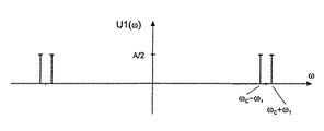
【0079】
このスペクトルは周波数ωc ±ω1 を持つ2個の重なった振動から構成される。これは理想サンプラーを用いて変換され、数学的に、かつスペクトルとして示されている(図2J参照)。
【0080】
その時、サンプリング周波数ωA は搬送周波数ωc の4分の1であり、ファクタνuds は4である。式(15)とさらに式(17)及び(18)を用いた同期的サンプリングにおける前提条件と同様の前提条件で、コンバータの出力信号U1(t)を得ることができる。
【数19】
図2Jは、同期的にアンダーサンプリングされた振幅変調信号のスペクトルを示す。
【0082】
図2Kの中で意味のある信号、すなわち0とサンプリング周波数の半分±ωA /2との間に位置する信号に注目し、
【数20】
【数21】
![]()
【0083】
図2Kは、0から±ωA /2までの、同期的にアンダーサンプリングされた、振幅変調信号のスペクトルを示す。
【0084】
この−ωA /2からωA /2までの領域のスペクトルは、n=〔−∞…−1,0,1…+∞〕として、nωA /2の後から(n+1)ωA /2まで周期的に反復される。
【0085】
さらなる計算領域は、理想ローパスフィルタによりωA /2までに制限されるか、あるいは、サンプリングされたセンサ出力信号の中で発生している高調波は、現実のローパスフィルタを用いて、それぞれ可能な限り減衰される。
【0086】
もしサンプリングの後で信号が直接的に出力されなければならず、もしωA /2とω1 とが互いに近い場合には、発生している高調波を可能な限り消すために、それに続くローパスフィルタは高いオーダー、すなわち非常に急峻な減衰特性を持つものでなければならない。
【0087】
考察と計算の結果、A/D変換器は基本的に第1復調段階で使用されるのがよいことがわかるであろう。A/D変換器あるいはサンプルホールド手段は、それぞれ、以下により詳細に説明する特別なフレーム条件を満たす必要がある
【0088】
センサと電子評価装置の間の最重要リンクは、特別な特性を備えたA/D変換器である。センサ信号のデジタル処理は、情報ロスなくサンプリングすることで数字のシーケンスに直接変換することを必要とする。いわゆるサンプルホールド手段は、この適用においては、ほぼ理想的なサンプリング手段としての役割を果たすことになる。すなわち、この手段はセンサ信号の非常に短い「サンプル」を取り出すだけでもよい。この場合、信号のいわゆる針で一刺するような抽出(pinprick−like taps)が実行されなければならず、そのため、取得時間すなわちサンプルが取られる時間が最も重要となる。
【0089】
本発明にかかる容量性センサ素子の出力信号をデジタル評価するための電子評価装置を用いれば、従来のアナログ電子評価装置に比べて多数の利点が得られる。
【0090】
本発明の理解を深めるために、また技術的な概念の利点を明確にするために、本発明の読取方法の原理を、図4を用いながら、図5に示される公知の読取方法と直接比較して説明する。
【0091】
図5に関して既に説明した通り、増幅されたアナログセンサ出力信号は、従来技術の読取方法により、信号を搬送周波数(例えば500kHz)で乗算することで復調される(図5参照)。
【0092】
本発明にかかる容量性センサのデジタル方式読取方法の概念では、図4に基本的に示されるように、センサ100の中央にある搬送周波数は信号源110から供給される。すなわち、搬送および駆動信号は、容量性センサ100の共通の中央電極から内部に向かって供給される。この容量性センサ100のセンサ出力信号は、センサ100の外部電極から外部に向かって抽出される。センサ信号は差動的に読み取られ、演算増幅器122を用いて増幅される。増幅されたアナログセンサ出力信号は、次にサンプルホールド手段を備えたアナログ/デジタル変換器を用いて復調され、このとき信号源110から供給されたサンプリング信号の周波数は搬送周波数を整数で割り算した数となる。これは通常、サンプリング信号が搬送信号と同期するような、信号発生器内での搬送信号の同期周波数分割により達成される。アナログ/デジタル変換器126の出力において、信号波形S5(図1参照)が離散的にサンプリングされた値のシーケンスとしてデジタル形式で存在する。このデジタル信号は、次にデジタル信号プロセッサ130により比較的小さな計算労力でさらに処理されてもよい。
【0093】
しかし、本発明の評価装置を用いて、搬送および駆動信号が容量性センサの外部電極102〜106、102’〜106’に対して外部から供給されるようにすることも、同様に可能である。この場合、例えば図1に示されるように、センサ出力信号はセンサ100の共通中央電極108から抽出されてもよい。
【0094】
図1に示された本発明の読取方法と、図5に示された従来技術の読取方法とを比較すると、次の点が明らかになる。すなわち、いわゆるアンダーサンプリング技術を用いると、それがセンサ出力信号の基本的には完全なデジタル処理であって、さらに比較的小さな計算労力でさらなるデジタル信号処理が可能であることから、複数の利点が得られる可能性があるという点である。
【0095】
特別に規定された時間を起点として変換処理を開始する可能性は、センサ出力信号のアンダーサンプリングの正確な持続を保証するために、センサ信号の評価にとって特に重要な意味を持つ。そのため、サンプルホールド手段を備えたこのA/D変換器の対応する帯域幅は、最高信号周波数に対応して選択されなければならない。本発明の原理のさらなる利点は、アナログからデジタル部分への変換が、センサ信号の第1増幅の直後に実行される点である。この場合、有効信号を制限するものは、第1(アナログ)増幅器の固有ノイズのみになる。その時、A/D変換器の量子化ノイズは、センサのノイズにより飲み込まれるという点に注目すべきである。
【0096】
そのため、容量性加速度センサにおいては、有効信号はこのアンダーサンプリング法を用いて直接的に評価されてもよい。なぜなら、A/D変換器は全体的な周波数領域に対してスペクトルをマップするからである。搬送評価周波数の直接除数としてのサンプリング周波数を適切に選択すれば、スペクトルはシフトされ、搬送信号がDC電圧のように現れ、この信号の振幅内の情報、すなわち加速度(静電容量)が測定信号の振幅に直接的に比例するようになる。
【0097】
例えば回転速度センサDAVED(登録商標)に使用されているように、容量性読取方法を用いれば、第1復調段階は省略されてもよい。なぜなら、これは既に特別なA/D変換器によって実行されているからである。この場合、交流信号が受信され、その振幅は測定された回転速度に対応する。もしこの信号が再度復調(第2復調)されれば、この復調はデジタル方式で計算され、かつ対応するアルゴリズムはデジタル信号プロセッサ(DSP)内で直接実行される。
【0098】
現実の情報(回転速度に比例したビットの組合せ)はデジタル信号プロセッサからデジタル方式で出力され、あるいはPWM(パルス幅変調)信号としてさらに処理される。これは有効信号のD/A変換におけるデータロスや追加的なノイズをそれぞれ阻止できるようにするためである。この方法により、電子回路のノイズは減衰され、センサの分解能は略達成されるであろう。
【0099】
異なる容量性センサ(ジャイロスコープ、加速度センサ、傾斜角センサ等)を備えた完全なセンサシステムの構築のために、この読取方法は理想的である。デジタル信号プロセッサ(DSP)内において、個々のセンサ信号は互いに比較され、それぞれ計算される。この時、最適化された規則アルゴリズムによってシステム全体の作業能力が向上する。
【0100】
もし、例えば異なる角度に位置する数個の回転速度センサが一緒に使用される場合には、対象物の動きや速度が決定されるであろう。微小機械的製造方法により、特定の注文生産された工業製品のために、低コスト、低インターフェイス(すなわち非常に信頼性が高い)、かつ最小型の回転速度センサを製造することも実現可能になるであろう。本発明のデジタル読取及び評価法を使用すれば、容量性回転速度センサにおいて、毎秒0.01°の領域に至る精度の回転運動が検出される可能性がある。
【0101】
本発明において、センサ信号評価のために使用されるデジタル信号プロセッサに対する要求や使用容量が減少したことで、これらデジタル信号プロセッサが、個々のセンサまたはセンサ全体のための追加的な仕事や機能を担うことも可能になる。それらは例えば、PIレギュレータを用いた能動的温度補償、自己測定および自己診断機能など、速度と柔軟性に起因する仕事や機能である。
【0102】
本発明にかかるデジタルセンサ信号読取装置の実際の構造を、図3を参照しながら説明する。図3は、一次及び二次制御回路を備えた容量性センサ素子のためのデジタル電子評価装置のブロック図である。図3内の要素で、図1内の要素に対応するものには、同じ参照符号を付して示す。
【0103】
ここで用いられるセンサは、図1の容量性センサ100に対応しており、駆動信号S1(ω+ drive )に対しては入力102が、180°位相シフトされた駆動信号S’1(ω− drive )に対しては入力102’が、搬送信号S2(ω+ cp)に対しては入力104が、180°位相シフトされた搬送信号S’2(ω− cp)に対しては入力104’が、搬送信号S3(ω+ cs)に対しては入力106が、180°位相シフトされた搬送信号S’3(ω− cs)に対しては入力106’が、それぞれ設けられている。一次および二次の搬送信号S2(ω+ cp),S’2(ω− cp),S3(ω+ cs),S’3(ω− cs)のための入力104,104’,106,106’に対しては、信号発生器110から送信され、センサ100の入力102,102’に対しては、+1または−1の増幅ファクタを使用する増幅器111からそれぞれ送信される。センサ100の出力信号はアナログ増幅器122により増幅される。増幅されたアナログセンサ出力信号はアナログハイパスフィルタ124により濾波される。
【0104】
フィルタ124の出力信号は、次にアナログ/デジタル変換器126,128の両方に対して供給され、これら変換器は、増幅され濾波されたアナログセンサ出力信号を、いわゆるアンダーサンプリング技術を用いてサンプリングする。このアンダーサンプリング技術においては、一方では搬送信号の周波数に同期性を持ち、他方では搬送信号の周波数の整数分の1である周波数が用いられる。このようなサンプリング周波数が、信号発生器110からアナログ/デジタル変換器126,128に対して供給される。
【0105】
サンプルホールド手段を用いたアナログ/デジタル変換器によりサンプリングされた後に、離散的にサンプリングされた値の結果としてデジタル形式で存在しているセンサ出力信号は、次にデジタル信号プロセッサ130に対して入力される。このデジタル信号プロセッサ130においては、アナログ/デジタル変換器126からの信号を一次回路で、アナログ/デジタル変換器128からの信号を二次回路で処理する。デジタル信号プロセッサは、デジタルバンドパスフィルタ132,134と、復調器136,138,140,142と、デジタルローパスフィルタ144,146,148,150と、コンパレータ152と、デジタルPIレギュレータ154,156,158,160と、クロック162と、一次正弦波発振器164と、二次正弦波発振器166とを備え、これらの部品はソフトウエアを内蔵し、図3に示されるように配置され、相互に接続されている。一次正弦波発振器164は、出力側でデジタル/アナログ変換器168に接続され、この変換器168は再び増幅器111へと接続されている。二次正弦波発振器166は、出力側でデジタル/アナログ変換器170とデジタル/アナログ変換器172とに接続され、これらの変換器170,172は再びセンサ100の入力106と入力106’とにそれぞれ接続されている。デジタルPIレギュレータ158の出力は、デジタル信号プロセッサ130の出力インターフェイス174に接続され、ここで出力信号すなわち検出されるべき回転速度が、デジタル形式またはアナログ形式で出力される。
【0106】
一次および二次制御回路を備えたデジタル信号評価装置を広範囲に活用することで、例えば温度ドリフトなど環境からの影響に対する補償作用を、従来の装置と比較して格段に発展させることができる。そのため、センサ出力信号の周波数と振幅の優れた安定性を達成することができる。
【図面の簡単な説明】
【図1】
本発明にかかるセンサ素子のためのデジタル信号電子評価装置のブロック図である。
【図2A】
サンプリングプロセスを示す図である。
【図2B】
ディラックと矩形パルスとを示す図である。
【図2C】
サンプラーのモデルを示す図である。
【図2D】
理想サンプリングの図である。
【図2E】
理想サンプリングプロセスをスペクトルで示した図である。
【図2F】
fA <fcs+fdrive での中間ミキシングを表した図である。
【図2G】
同期的にサンプリングされた余弦波振動のスペクトル図である。
【図2H】
同期的にサンプリングされた余弦波振動の時間的経過を示す図である。
【図2I】
振幅変調された信号のスペクトル図である。
【図2J】
同期的にアンダーサンプリングされた振幅変調信号のスペクトル図である。
【図2K】
0から±ωA /2までの同期的にアンダーサンプリングされた振幅変調信号のスペクトル図である。
【図2L】
バンドパスフィルタを用いて同期的にアンダーサンプリングされた振幅変調信号のスペクトル図である。
【図3】
一次および二次の制御回路を備えた容量性センサ素子のためのデジタル信号電子評価装置のブロック図である。
【図4】
本発明のデジタル信号評価装置の主要部を示す回路図である。
【図5】
従来のアナログ信号評価装置の主要部を示す回路図である。
【図6】
センサ装置のための従来のアナログ信号評価電子装置のブロック図である。
【符号の説明】
100 センサ
102,102’ 駆動信号入力電極
104,104’ 一次搬送信号入力電極
106,106’ 二次搬送信号入力電極
120 デジタル評価電子装置
122 演算増幅器
124 アナログハイパスフィルタ
126,128 アナログ/デジタル変換器
130 デジタル信号プロセッサ[0001]
The present invention relates to sensor reading, and more particularly, to digital processing of a sensor output signal with a high frequency carrier signal modulated by a measurement. In the following description of the present invention, reference will be made to capacitive sensors, such as micromechanical rotational speed sensors that use Coriolis forces to detect rotational speed, to explain the inventive concept.
[0002]
Capacitive sensors, such as micromechanical rotational speed sensors, have various applications. It is used, for example, in robots and packaging systems, and in medical technology. Further, they are used in cameras for image stabilization, in navigation systems for stabilizing and remotely controlling cars and aircraft, and in airbags and security systems. In general, such sensors comprise a movable mechanical structure in which periodic oscillations are excited. The periodic vibration generated by this excitation can also be called primary vibration. If the sensor is subject to rotation about this primary vibration or an axis perpendicular to the primary motion, the motion of the primary vibration will generate a Coriolis force proportional to the measured quantity or angular velocity. The Coriolis force excites a second vibration orthogonal to the primary vibration. The second vibration orthogonal to the primary vibration is called secondary vibration. The secondary vibration is also called a detected vibration, and is detected by, for example, a capacitive measurement method. This capacitively measured quantity serves as a measure for the rotational speed acting on the rotational speed sensor.
[0003]
Thus, in micro-technical sensors, electronic signal evaluation plays a very important role, as the performance of the overall sensor system is largely determined by the reading and electronic evaluation equipment used. Existing rotational speed sensors with small micro-mechanical structures, such as the rotational speed sensor DAVED® developed by Micron and Information Technology Laboratories of Hahn Sickert, have about 10-18 Very small capacitances and capacitance changes until reaching the region of F (Coriolis parameter) must be detected, and only very small voltages are received as sensor output signals, but these may not be directly evaluated. There is.
[0004]
In a micromechanical rotation speed sensor, the sensor output signal is limited mainly by noise of electronic components of the electronic evaluation device. This is because the actual information contained in the sensor output signal of the rotational speed sensor is generally indistinguishable from noise below a certain level and therefore undetectable.
[0005]
FIG. 6 shows a block diagram of a typical conventional
[0006]
The
[0007]
The use of a high-frequency carrier signal can significantly improve the S / N ratio of the sensor output signal. In this case, in realizing an electronic signal evaluation device using analog components, reproduction of a valid signal from an amplitude-modulated (AM-modulated) sensor output signal is performed by double demodulation in the electronic
[0008]
The amplitude modulated sensor output signal is sent to an (analog)
[0009]
Next, the signal S5 is sent to a second demodulator (multiplier II) 330, where the sinusoidal AC signal S5 is converted to a DC current signal or DC voltage S6, respectively. Since S6 is directly proportional to the amplitude of the alternating current signal, it is also proportional to the measured amount. This multiplication is performed using a low-frequency DC voltage that is phase-shifted to a drive voltage S1.
[0010]
In order to describe in more detail the above-mentioned known method of reading and evaluating the analog sensor output signal and to make it easier to compare with the reading and evaluating method of the present invention, the principle of the reading and evaluating method in the prior art is described. The summary will be described again with reference to FIG.
[0011]
Carrier signal ωc (For example, 500 kHz) is supplied from the
[0012]
The main problem with this conventional sensor device is that the first demodulation of the sensor signal must be performed with a high-frequency carrier signal (eg, 500 kHz). Therefore, in oversampling the carrier signal, the digital signal processor had to work with a clock frequency higher than twice the carrier frequency. This may not be reasonably achievable with current digital signal processors because a very large amount of computational operations will occur.
[0013]
A further problem with the conventional sensor device described above is that, in addition to the inherent noise of the first (analog)
[0014]
Based on the above prior art, it is an object of the present invention to provide a more developed concept for processing the output signal of a sensor in order to improve the measurement accuracy and sensitivity of the sensor device.
[0015]
The above object can be achieved by a method for processing an analog output signal of a sensor according to
[0016]
The present invention is based on the following findings. That is, it is a finding that processing of a sensor output signal of a sensor element, for example, a capacitive rotation speed sensor or the like can be significantly improved by using digital processing technology.
[0017]
According to the invention, the output signal of the sensor element is input to a digital signal processor (DSP) using an analog to digital converter (A / D converter) using a sample and hold means, and the valid signal is Here, it is digitally processed and evaluated.
[0018]
The sensor according to the invention so that the amplitude-modulated sensor signal carried on the high-frequency carrier signal is appropriately transmitted to the digital signal processor so that the digital signal processor can detect and output the measured quantity to be detected with relatively little computational effort. In output signal processing, the so-called undersampling principle is used.
[0019]
The principle of undersampling described above according to the invention is that all sensors whose output signal comprises a typical high-frequency carrier signal and whose high-frequency carrier signal is modulated by a measurand, such as, for example, amplitude modulation, in particular, It can be used for capacitive sensors. Using this principle, the high-frequency carrier signal in the sensor device is first modulated based on the measurement signal. Thereafter, rather than being demodulated with the high frequency signal as known in the prior art, the measurement signal is processed by a digital signal processor using an A / D converter with sample and hold means using a lower sampling frequency. It is converted into an effective signal that is easy to use. By selecting the "appropriate" sampling frequency for the undersampling process, the sensor output, which is a sampled sensor output signal and whose amplitude is proportional to the measurand, is directly converted to digital data by a digital signal processor. And the measured quantity is detected.
[0020]
This means that, in the case of a capacitive rotational speed sensor, when a differential read-out method is used, the amplitude of the effective signal is proportional to the capacitance of the capacitive sensor element and the change in capacitance, respectively. It is.
[0021]
As described above, with the present invention, the analog output signal of the sensor will be conveniently processed. There, the analog sensor output signal comprises a high-frequency carrier signal modulated (eg, amplitude modulated) by a measurand. The aforementioned "proper" selection of the sampling frequency of the sampling signal is a critical factor in the principle of undersampling used in the present invention.
[0022]
In the present invention, the analog sensor output signal is sampled using an A / D converter having a sample and hold unit. At this time, the sampling frequency is set so that the carrier frequency of the sensor output signal is an integral multiple of the sampling frequency.
[0023]
Carrier frequency ω of capacitive sensorc Is usually the frequency ω of the useful signaldrive The sensor output signal is also sampled at a lower frequency than the carrier frequency so that the useful signal can be completely reconstructed, ie without loss of information, since it is 30 to 500 higher than the factor. May be. At the same time, the phase of the sampling signal must be selected to synchronize with the carrier signal in the sensor output signal. This is achieved, for example, by synchronous frequency division of the carrier signal. In order to obtain a useful signal from the sampled sensor output signal, the sampled sensor output signal is filtered, i.e., filtered by a band-pass filter, in order to remove the higher frequency signal portions that repeat periodically therein. Must be applied. At this time, the amplitude of the signal filtered by the band-pass filter, that is, the effective signal, is proportional to the measured amount detected by the sensor. The filtering by this bandpass filter and the further processing of the sampled sensor output signal are performed digitally in a digital signal processor (DSP) following the A / D converter.
[0024]
From the received useful signal, the measured quantity to be detected, such as the rotational speed, is detected by the digital signal processor without significant computational effort. The overall (digital) signal processing and evaluation, i.e. sampling and filtering of the sensor output signal and determination of the measurand, are performed by a single digital signal processor, since undersampling eliminates extensive computational work. Is possible.
[0025]
The ability to process the sensor output signal of the sensor element using a basically digital signal processor has several advantages.
[0026]
The possibility of starting the conversion process at a specially set time is very important for the evaluation of the sensor signal in order to ensure that the undersampling of the sensor output signal is exactly maintained. Therefore, the corresponding bandwidth of this A / D converter with sample and hold means must be selected corresponding to the highest signal frequency. A further advantage of this principle is that the conversion from analog to digital part is performed immediately after the first amplification of the sensor signal, in which case the useful signal is reduced by the inherent noise of the first (analog) amplifier. Only restricted.
[0027]
In a capacitive sensor, such as a capacitive acceleration sensor, the effective signal is directly evaluated using this undersampling method because the A / D converter maps the spectrum over the entire frequency domain. Is also good.
[0028]
If the sampling frequency as a direct divisor of the carrier evaluation frequency is appropriately selected, the carrier frequency is shifted to the zero point (f = 0 Hz), and information within the amplitude of this signal, that is, acceleration (capacity) is directly measured signal. Can be shifted in proportion to the amplitude of
[0029]
In a differential capacitance reading method, the first demodulation stage may be omitted, as for example in a rotational speed sensor DAVED®. Because it has already been performed by a special A / D converter. In this case, an AC voltage is obtained, the amplitude of which corresponds to the rotation speed. If the signal is demodulated again (second demodulation stage), the demodulation is calculated directly and the corresponding algorithm is executed directly in a digital signal processor (DSP).
[0030]
The actual information (bit combination proportional to the rotation speed) is output digitally from a digital signal processor, or by means of a feasible D / A conversion of the useful signal, respectively, to prevent data loss and the addition of noise. Is further processed as a PWM signal (PWM = pulse width modulation). In this way, the noise of the electronic circuit is reduced and the practical resolution of the sensor will be substantially achieved.
[0031]
This reading method is ideal for setting up a complete sensor system with different capacitive sensors (gyroscope, acceleration sensor, tilt angle sensor, etc.). Within a digital signal processor (DSP), the individual sensor signals will be compared or otherwise calculated with each other, and the performance of the overall system will be improved using optimal control algorithms.
[0032]
For example, when a plurality of rotation speed sensors are used at different angles at the same time, the movement and speed of the object are detected. Thus, the micromechanical manufacturing process allows low cost, low interface (i.e., very reliable), and smallest rotational speed sensors to be made for a particular bespoke industrial product. . According to the digital reading evaluation method of the present invention, it will be possible for a capacitive rotational speed sensor, for example, to detect a rotational movement even in a range of about 0.01 ° per second.
[0033]
In the present invention, the reduced signal processing demands on digital signal processors used for sensor signal evaluation make these digital signal processors play an additional role or function for individual sensors or for the entire sensor. It becomes possible. These include, for example, active temperature compensation using PI regulators, self-measurement and self-diagnosis functions.
[0034]
Hereinafter, preferred embodiments of the present invention will be described with reference to the accompanying drawings.
FIG. 1 shows a block diagram of a digital signal electronic evaluation device for a sensor element according to the present invention,
2A-2L illustrate the process of undersampling with digital evaluation of the output signal of a capacitive sensor;
FIG. 3 is a block diagram of a digital signal electronic evaluation device for a capacitive sensor element with primary and secondary control circuits;
FIG. 4 shows a main part of the digital signal evaluation device of the present invention,
FIG. 5 shows a main part of a conventional analog signal evaluation device,
FIG. 6 is a block diagram of a conventional analog signal evaluation electronic device for a sensor device.
[0035]
FIG. 1 shows a block diagram of a digital reading and
[0036]
The
[0037]
In the case of a capacitive rotational speed sensor, a small amount of capacitance or a change in capacitance is also 10-18 Only a small amount of voltage which must be detected to the extent of F and cannot be directly evaluated is received as a sensor output signal. By using a high-frequency carrier signal modulated by the detected measurand, the S / N ratio of the sensor output signal is significantly improved.
[0038]
In the case of the sensor device described above as prior art, the amplitude-modulated output signal of the sensor with the high-frequency carrier signal is first sent to an (analog) operational amplifier, where it is amplified.
[0039]
An
[0040]
The amplified sensor output signal is sent to a high-
[0041]
[0042]
Hereinafter, the function and method of the apparatus for processing the analog output signal S4 of the
[0043]
In the sensor evaluation device according to the present invention, the carrier frequency ω is an analog sensor output signal and is modulated by the measured amount.c An output signal having a carrier signal having a sampling frequency ω is obtained by using A /
[0044]
As described above, the use of a high-frequency carrier signal can significantly improve the S / N ratio of the sensor output signal, and in a capacitive sensor, the carrier frequency ω of the carrier signalc Is typically set higher than 250 kHz, preferably around 500-750 kHz.
[0045]
Carrier frequency ω of capacitive sensorc Is usually the frequency ω of the useful signaldrive The sensor output signal may also be sampled at a lower frequency than the carrier frequency in order to reconstruct the useful signal completely, i.e. without information loss, by a factor of 30-500 above. At that time, the phase of the sampling signal must be set so that the sampling signal is synchronized with the carrier signal. This is substantially achieved by synchronous frequency division of the carrier signal, in which case the carrier frequency ω of the carrier signalc Is the sampling frequency ωA Is an integer multiple of. That is, ωC = NωA Becomes Therefore, the sensor output signal exists in digital form as a sequence of discretely sampled values after sampling by the A / D converter using the sample and hold means.
[0046]
The digital sampled sensor output signal is further subjected to digital processing in the
[0047]
Since the amplitude of the effective signal present at this point is proportional to the measurand, e.g., rotational speed, detected by
[0048]
In summary, the sensor output signal is converted into a valid signal using so-called undersampling and using A /
[0049]
It should be noted that the concept of the present invention for processing the analog output signal of the sensor applies to all analog sensor output signals with a carrier signal modulated by the measurand, in particular the output signal of a capacitive sensor. It is available.
[0050]
In the following, the system theoretical aspects of the present invention that underlie the implementation of undersampling will be described in more detail.
[0051]
Ideal sampling is time t = nTA (Where n =... -1, 0, 1,...) Represents a continuous signal u (t) by a sequence of equidistant impulses. Therefore, the impulse area of each value is represented by the time (nTA ) (See FIG. 2A: sampling process).
[0052]
Sampling period TA = 1 / fA Is the sampling time interval. For the purpose of illustrating the sampled function values, a pulse g (t) normalized to 1 is used, as illustrated in FIG. 2B (see Dirac and rectangular pulses).
[0053]
The sampler is described using a theoretical model. The pulse shape of the sampler describes a Dirac pulse, and the function ε (t) indicates a jump function. Therefore, the sampler calculates the input value ue1And ue2As a simple model of a multiplier with As a result, the output value ua Is again the multiplier constant UM Combined with
(Equation 1)
(Equation 3)
In this way, the sampler model shown in FIG. 2C is obtained.
[0054]
Here, the main principle of the invention is to use this multiplier as a mixer and as a first demodulation stage.
[0055]
To explain this key principle in more detail, further considerations are needed, especially in the spectral domain.
[0056]
The shaping filter is represented by δ (t−nTA ). As an equation for a real sampler, the following equation is obtained.
(Equation 4)
(Equation 5)
[0057]
For the calculation in the frequency domain, the spectrum of the sampling signal must be calculated. This is performed by multiplying the spectrum of the ideal sampler by the frequency response of the shaping filter. The frequency response is a Fourier transform of the pulse response function g (t). function
(Equation 6)
(Equation 7)
[0058]
The spectrum of the ideal sampler is the Dirac pulse sequence δper When (t) is expanded in the Fourier sequence, the following expression is obtained.
(Equation 8)
(Equation 9)
(Equation 10)
[0059]
Further transformation and simplification results in the following equation:
(Equation 11)
[0060]
The use of a sampler as the demodulation stage is described in more detail in the time domain, using this frequency domain knowledge and a graphical description of the signal.
[0061]
In order for the signal to be digitized and then fully reproduced, further conditions need to be met. In this sense, this is referred to as a sampling law. It indicates that analog signals must be band limited. That is, so that the original signal is completely reconstructed without any information loss, the signal cutoff frequency fgsBeyond, no spectral components should be located. Therefore, for some signal spectrum U (f), | f | ≧ fgsMust satisfy the condition U (f) = 0.
[0062]
Therefore, the sampling frequency fA Must be at least twice as high as the signal cutoff frequency.
(Equation 12)
In order to prevent overlap with the periodic repetition of the spectrum of u (t), so-called aliasing, both conditions must be met. This is because the aliasing effect may hinder the complete reconstruction of the signal.
[0064]
In order to meet the sampling law, the frequency for digitization needs to be at least twice as high as the highest frequency present in the signal.
[0065]
If this condition, that is to say the sampling law, is applied to the electronic evaluation device of the invention for a sensor, for example a capacitive rotational speed sensor, then this frequency is respectively fA ≧ 2 (fcs+ Fdrive ) Or fA ≧ 2 (fcp+ Fdrive ). Since the signal-to-noise ratio, ie the ratio of the amplitude of the transmitted signal to the noise amplitude, must be as high as possible, the carrier frequency must be as high as possible, for example several hundred kHz. If the carrier frequency is 500 kHz or higher, the sampling rate must be 1 MHz or higher.
[0066]
As a result of the processing in this clock cycle, an enormous amount of data is generated. That is, when the cutoff frequency of the sensor is set to 100 Hz, the change in rotation speed is detected at a cycle of 10 msec at the maximum. The information to completely map the drive frequency (1-10 kHz) is 10,000 vibrations per second. Assuming that the carrier frequency is, for example, 500 kHz, the sampling process must be performed at a frequency of 1 MHz according to the sampling rule. This means a factor of 10,000 for a bandwidth of 100 Hz. Therefore, for a higher carrier frequency compared to the required information, the sampling is 100 × 10000 (= 1 × 10⁶ ) Must be performed.
[0067]
As shown in FIG. 2C (model of the sampler), the sampler consists of a multiplier and a shaping filter. Therefore, it is clear that the characteristics of the multiplier and the shaping filter are used for the purpose of so-called intermediate mixing, synchronous sampling or undersampling having predetermined characteristic values and limit values, respectively.
[0068]
In the above-mentioned intermediate mixing, 0 to fA And nfA ~ (N + 1) fA In this range, the output signal of the ideal sampler is the same, and the characteristic that the band-limited signal including the DC component is not evaluated is used. This allows the signal width containing the necessary information to be "shifted" within the range in which the total number of data is reprocessed. In FIG. 2F, the so-called intermediate mixing is fA <Fcs+ Fdrive Is represented by
[0069]
With an appropriate choice of the sampling frequency, it is possible to shift the effective frequency directly to zero, so that the first demodulation by the sampling means or the integrated analog / digital converter can be realized respectively. Will be possible.
[0070]
At that time, the frequency ω0 And the length of the same period TA = 1 / ω0 The vibration with is sampled. At the starting point, an ideal sampler is used, where the integration of the real sampler with the characteristic additional frequency response sin (x) / x does not affect the considerations here.
[0071]
Expression (11) is used as an expression indicating the sampled vibration,
(Equation 13)
[Equation 14]
(Equation 15)
[0072]
An equidistant sampling value with frequency components appearing in the spectrum is obtained, which value is represented by a coefficient n. FIG. 2G shows the spectrum of a cosine wave oscillation sampled synchronously. Synchronous sampling is graphically represented in the time domain with the following signal image, and FIG. 2H shows the time course of the synchronously sampled cosine oscillation.
[0073]
With this process, the total number of "possible signals" appears to be infinite. That is, the sampling value may be any multiple starting from zero times the sampling frequency. If the signal in the digital signal processing is from the DC voltage portion to half the sampling frequency, the above processing corresponds to the frequency shift to the zero point on the frequency axis and corresponds to demodulation. The separation of high-frequency components is performed theoretically by an ideal low-pass filter whose cut-off frequency corresponds to half the sampling frequency.
(Equation 16)
In the circuit structure, the separation of the high-frequency component is realized by a low-pass filter having a steepest attenuation characteristic using software, for example, and attenuating unnecessary harmonics as strongly as possible. .
[0075]
As mentioned above, when the sampling process is synchronized with the carrier signal, the sampler may be used to determine the amplitude and phase of the oscillation, ie as a first demodulation stage.
[0076]
As a factor for the frequency distance from the wave to be detected to the vibration carrying the information in the range of 30 to 500 (ie the ratio of the frequency of the carrier signal to the frequency of the useful signal), all synchronous values are It does not need to be used and allows further undersampling of the signal.
[0077]
Undersampling factor νuds Is the sampling frequency ωA Vibration frequency ωcsShows the ratio of
[Equation 17]
This process will be described in further detail in the example shown below. For example, this factor νuds Is selected as 4. Amplitude modulated signal
(Equation 18)
[0079]
This spectrum has a frequency ωc ± ω1 It consists of two overlapping vibrations with This has been transformed using an ideal sampler and is shown mathematically and as a spectrum (see FIG. 2J).
[0080]
At that time, the sampling frequency ωA Is the carrier frequency ωc And a factor νuds Is 4. The output signal U1 (t) of the converter can be obtained under the same precondition as the precondition in the synchronous sampling using the equation (15) and the equations (17) and (18).
[Equation 19]
FIG. 2J shows the spectrum of an amplitude modulated signal that is synchronously undersampled.
[0082]
Significant signals in FIG. 2K, ie, 0 and half the sampling frequency ± ωA Note the signal located between
(Equation 20)
(Equation 21)
![]()
[0083]
FIG. 2K shows that from 0 to ±
[0084]
This -ωA / 2 to ωA The spectrum in the region up to / 2 is given by n = [− ∞... −1, 0, 1.A / N after (n + 1) ωA / 2 is repeated periodically.
[0085]
A further calculation area is ω by an ideal low-pass filter.A / 2, or harmonics occurring in the sampled sensor output signal are each attenuated as much as possible using real low-pass filters.
[0086]
If the signal must be output directly after sampling, if ωA / 2 and ω1 Is close to each other, the following low-pass filter must be of a high order, that is, have a very steep attenuation characteristic, in order to eliminate generated harmonics as much as possible.
[0087]
It will be understood from consideration and calculation that the A / D converter is basically preferably used in the first demodulation stage. The A / D converter or the sample-and-hold means must each meet special frame conditions, which will be described in more detail below.
[0088]
The most important link between the sensor and the electronic evaluation device is an A / D converter with special characteristics. Digital processing of sensor signals requires direct conversion to a sequence of numbers by sampling without loss of information. The so-called sample-and-hold means will serve as an almost ideal sampling means in this application. That is, the means may only take a very short "sample" of the sensor signal. In this case, a so-called pinprick-like tap of the signal must be performed, and therefore the acquisition time, ie the time when the sample is taken, is of utmost importance.
[0089]
The use of an electronic evaluation device for digitally evaluating the output signal of a capacitive sensor element according to the present invention provides a number of advantages over conventional analog electronic evaluation devices.
[0090]
For a better understanding of the invention and to clarify the advantages of the technical concept, the principle of the reading method of the present invention is compared directly with the known reading method shown in FIG. Will be explained.
[0091]
As previously described with respect to FIG. 5, the amplified analog sensor output signal is demodulated by multiplying the signal by a carrier frequency (eg, 500 kHz) according to prior art reading methods (see FIG. 5).
[0092]
In the concept of a digital reading method of a capacitive sensor according to the invention, the carrier frequency at the center of the
[0093]
However, it is equally possible for the transport and drive signals to be supplied externally to the external electrodes 102-106, 102'-106 'of the capacitive sensor using the evaluation device of the invention. . In this case, for example, as shown in FIG. 1, the sensor output signal may be extracted from the
[0094]
When the reading method of the present invention shown in FIG. 1 is compared with the conventional reading method shown in FIG. 5, the following points become clear. That is, the use of the so-called undersampling technique has several advantages because it is basically completely digital processing of the sensor output signal and further digital signal processing can be performed with relatively little computational effort. The point is that it can be obtained.
[0095]
The possibility of starting the conversion process from a specially defined time is particularly important for the evaluation of the sensor signal in order to ensure the correct duration of the undersampling of the sensor output signal. Therefore, the corresponding bandwidth of this A / D converter with sample and hold means must be selected corresponding to the highest signal frequency. A further advantage of the principles of the present invention is that the conversion from analog to digital portion is performed immediately after the first amplification of the sensor signal. In this case, what limits the effective signal is only the inherent noise of the first (analog) amplifier. At this time, it should be noted that the quantization noise of the A / D converter is swallowed by the noise of the sensor.
[0096]
Therefore, in a capacitive acceleration sensor, the effective signal may be directly evaluated using this undersampling method. This is because the A / D converter maps the spectrum to the entire frequency domain. With an appropriate choice of the sampling frequency as a direct divisor of the carrier evaluation frequency, the spectrum is shifted, the carrier signal appears like a DC voltage, and the information in the amplitude of this signal, ie the acceleration (capacitance), is the measurement signal Is directly proportional to the amplitude of
[0097]
For example, the first demodulation step may be omitted if a capacitive reading method is used, as used in a rotational speed sensor DAVED (registered trademark). This is because this has already been performed by a special A / D converter. In this case, an alternating signal is received, the amplitude of which corresponds to the measured rotational speed. If the signal is demodulated again (second demodulation), the demodulation is calculated digitally and the corresponding algorithm is executed directly in a digital signal processor (DSP).
[0098]
The actual information (combination of bits proportional to the rotational speed) is output digitally from a digital signal processor or further processed as a PWM (pulse width modulation) signal. This is to prevent data loss and additional noise in the D / A conversion of the effective signal. In this way, the noise of the electronics will be attenuated and the resolution of the sensor will be substantially achieved.
[0099]
This reading method is ideal for building a complete sensor system with different capacitive sensors (gyroscope, acceleration sensor, tilt angle sensor, etc.). Within a digital signal processor (DSP), the individual sensor signals are compared with one another and calculated respectively. At this time, the work efficiency of the entire system is improved by the optimized rule algorithm.
[0100]
If, for example, several rotational speed sensors located at different angles are used together, the movement or speed of the object will be determined. Micromechanical manufacturing methods also make it feasible to manufacture low cost, low interface (ie, very reliable), and minimal rotational speed sensors for specific tailor-made industrial products. Will. Using the digital reading and evaluation method of the present invention, a capacitive rotational speed sensor may detect rotational motion with an accuracy down to the 0.01 ° / sec range.
[0101]
In accordance with the present invention, the reduced demand and / or capacity of digital signal processors used for sensor signal evaluation has resulted in these digital signal processors taking on additional tasks and functions for individual sensors or for the entire sensor. It becomes possible. These are tasks and functions that result from speed and flexibility, such as active temperature compensation using PI regulators, self-measurement and self-diagnosis functions.
[0102]
The actual structure of the digital sensor signal reading device according to the present invention will be described with reference to FIG. FIG. 3 is a block diagram of a digital electronic evaluation device for a capacitive sensor element with primary and secondary control circuits. Elements in FIG. 3 that correspond to elements in FIG. 1 are given the same reference numerals.
[0103]
The sensor used here corresponds to the
[0104]
The output signal of the
[0105]
After being sampled by the analog / digital converter using the sample and hold means, the sensor output signal present in digital form as a result of the discretely sampled values is then input to a
[0106]
By making extensive use of a digital signal evaluation device having primary and secondary control circuits, the effect of compensating for environmental influences, such as, for example, temperature drift, can be significantly improved compared to conventional devices. Therefore, excellent stability of the frequency and amplitude of the sensor output signal can be achieved.
[Brief description of the drawings]
FIG.
1 is a block diagram of a digital signal electronic evaluation device for a sensor element according to the present invention.
FIG. 2A
FIG. 3 illustrates a sampling process.
FIG. 2B
It is a figure which shows Dirac and a rectangular pulse.
FIG. 2C
It is a figure showing a model of a sampler.
FIG. 2D
It is a figure of ideal sampling.
FIG. 2E
FIG. 3 is a diagram showing an ideal sampling process in a spectrum.
FIG. 2F
fA <Fcs+ Fdrive FIG. 7 is a diagram showing intermediate mixing in FIG.
FIG. 2G
FIG. 3 is a spectrum diagram of cosine wave oscillation sampled synchronously.
FIG. 2H
It is a figure which shows the time progress of the cosine wave oscillation sampled synchronously.
FIG. 2I
FIG. 3 is a spectrum diagram of an amplitude-modulated signal.
[FIG. 2J]
FIG. 4 is a spectrum diagram of an amplitude modulation signal that is synchronously undersampled.
FIG. 2K
0 to ± ωA FIG. 5 is a spectrum diagram of an amplitude modulation signal that is synchronously undersampled up to / 2.
FIG. 2L
FIG. 4 is a spectrum diagram of an amplitude modulation signal synchronously undersampled using a bandpass filter.
FIG. 3
FIG. 3 is a block diagram of a digital signal electronic evaluation device for a capacitive sensor element with primary and secondary control circuits.
FIG. 4
FIG. 2 is a circuit diagram showing a main part of the digital signal evaluation device of the present invention.
FIG. 5
FIG. 10 is a circuit diagram showing a main part of a conventional analog signal evaluation device.
FIG. 6
1 is a block diagram of a conventional analog signal evaluation electronics for a sensor device.
[Explanation of symbols]
100 sensors
102, 102 'drive signal input electrode
104, 104 'primary carrier signal input electrode
106,106 'Secondary carrier signal input electrode
120 Digital Evaluation Electronics
122 operational amplifier
124 Analog High Pass Filter
126,128 analog / digital converter
130 Digital Signal Processor
Claims (15)
サンプリング周波数ωA を用いて上記アナログセンサ出力信号(S4)をサンプリング(126,128)し、サンプリングされたセンサ出力信号を得る工程を備え、
上記サンプリング信号のサンプリング周波数ωA は搬送周波数ωc の整数n分の1に設定され、かつ上記サンプリング信号が上記搬送信号と同期するように上記サンプリング信号の位相が設定されていることを特徴とする方法。A method of processing an analog output signal (S4) of a sensor (100), said analog sensor output signal (S4) comprising a carrier signal having a carrier frequency ω c and modulated by a measurand.
Sampling the analog sensor output signal (S4) using the sampling frequency ω A (126, 128) to obtain a sampled sensor output signal;
The sampling frequency ω A of the sampling signal is set to an integer 1 / n of the carrier frequency ω c , and the phase of the sampling signal is set such that the sampling signal is synchronized with the carrier signal. how to.
上記サンプリング信号は搬送信号の同期周波数分割により得られ、上記搬送信号の搬送周波数ωc はサンプリング周波数ωA に整数倍数nを乗じたもの、すなわちωc =nωA であることを特徴とする方法。The method of claim 1, wherein
The sampling signal is obtained by synchronous frequency division of the carrier signal, and the carrier frequency ω c of the carrier signal is obtained by multiplying the sampling frequency ω A by an integer multiple n, that is, ω c = nω A. .
上記搬送信号の搬送周波数ωc は250kHz以上の周波数に設定されていることを特徴とする方法。The method according to claim 1 or 2,
The method according to claim 1, wherein the carrier frequency ω c of the carrier signal is set to a frequency of 250 kHz or more.
上記搬送信号の搬送周波数ωc は有効信号の周波数ωdrive よりも30〜500のファクタだけ高いことを特徴とする方法。The method according to any one of claims 1 to 3,
The method of claim 1 wherein the carrier frequency ω c of the carrier signal is higher than the frequency ω drive of the useful signal by a factor of 30 to 500.
上記アナログセンサ出力信号(S4)は上記サンプリング工程の前にアナログ方式で増幅されることを特徴とする方法。The method according to any one of claims 1 to 4,
The method according to claim 1, wherein the analog sensor output signal (S4) is amplified in an analog manner before the sampling step.
上記アナログセンサ出力信号(S4)の低周波数成分を本質的に取り除くために、上記増幅されたアナログセンサ出力信号は、上記サンプリング工程の前にハイパスフィルタにより濾波されることを特徴とする方法。The method according to any one of claims 1 to 5,
The method according to claim 1, characterized in that the amplified analog sensor output signal is filtered by a high-pass filter before the sampling step in order to essentially remove low frequency components of the analog sensor output signal (S4).
上記アナログセンサ出力信号(S4)は上記測定量により振幅変調されることを特徴とする方法。The method according to any one of claims 1 to 6,
The method according to claim 1, wherein the analog sensor output signal (S4) is amplitude-modulated by the measured quantity.
上記測定量は回転速度であることを特徴とする方法。The method according to any one of claims 1 to 7,
The method wherein the measured quantity is a rotational speed.
上記センサ(100)は容量性センサであることを特徴とする方法。The method according to any one of claims 1 to 8,
The method wherein the sensor (100) is a capacitive sensor.
上記容量性センサ(100)は容量性回転速度センサであることを特徴とする方法。The method of claim 9, wherein
The method of claim 1, wherein said capacitive sensor (100) is a capacitive rotational speed sensor.
上記搬送信号は上記センサ(100)に対して中央電極から入力され、上記センサ出力信号は上記センサ(100)の外部電極から出力されることを特徴とする方法。The method according to any one of claims 1 to 10,
The method of claim 1, wherein the transport signal is input to the sensor (100) from a central electrode, and the sensor output signal is output from an external electrode of the sensor (100).
上記搬送信号は上記センサ(100)に対して外部電極から入力され、上記センサ出力信号はセンサの共通電極(108)から出力されることを特徴とする方法。The method according to any one of claims 1 to 10,
A method according to claim 1, wherein said transport signal is input from an external electrode to said sensor (100) and said sensor output signal is output from a common electrode (108) of said sensor.
上記有効信号はデジタル信号プロセッサ(130)に対して入力され、上記デジタル信号プロセッサは測定量を表すアナログまたはデジタル信号を出力することを特徴とする方法。The method according to any one of claims 1 to 12,
The method of claim 1, wherein the valid signal is input to a digital signal processor (130), wherein the digital signal processor outputs an analog or digital signal representing the measured quantity.
上記装置は、サンプリングされたセンサ出力信号を得るために、サンプリング周波数ωA を用いて上記アナログセンサ出力信号(S4)をサンプリングするサンプリング装置(126,128)を備え、
サンプリング信号の上記サンプリング周波数ωA は搬送周波数ωc の整数n分の1に設定され、かつサンプリング信号が搬送信号と同期するようにサンプリング信号の位相が設定されていることを特徴とする装置。An apparatus for processing an analog output signal (S4) of a sensor (100), said analog sensor output signal (S4) comprising a carrier signal having a carrier frequency ω c and modulated by a measurand,
The apparatus, in order to obtain a sampled sensor output signal, comprising a sampling device (126, 128) for sampling the analog sensor output signal (S4) using a sampling frequency omega A,
The apparatus according to claim 1, wherein the sampling frequency ω A of the sampling signal is set to 1 / n of the integer of the carrier frequency ω c and the phase of the sampling signal is set so that the sampling signal is synchronized with the carrier signal.
Applications Claiming Priority (2)
| Application Number | Priority Date | Filing Date | Title |
|---|---|---|---|
| DE10059775A DE10059775C2 (en) | 2000-12-01 | 2000-12-01 | Method and device for processing analog output signals from capacitive sensors |
| PCT/EP2001/014022 WO2002044741A1 (en) | 2000-12-01 | 2001-11-30 | Method and device for processing analogue output signals from capacitive sensors |
Publications (2)
| Publication Number | Publication Date |
|---|---|
| JP2004526942A true JP2004526942A (en) | 2004-09-02 |
| JP2004526942A5 JP2004526942A5 (en) | 2005-04-28 |
Family
ID=7665445
Family Applications (1)
| Application Number | Title | Priority Date | Filing Date |
|---|---|---|---|
| JP2002546232A Pending JP2004526942A (en) | 2000-12-01 | 2001-11-30 | Method and apparatus for processing an analog output signal of a capacitive sensor |
Country Status (6)
| Country | Link |
|---|---|
| US (1) | US7054778B2 (en) |
| EP (1) | EP1337861B1 (en) |
| JP (1) | JP2004526942A (en) |
| AT (1) | ATE443872T1 (en) |
| DE (1) | DE10059775C2 (en) |
| WO (1) | WO2002044741A1 (en) |
Cited By (5)
| Publication number | Priority date | Publication date | Assignee | Title |
|---|---|---|---|---|
| JP2006170914A (en) * | 2004-12-17 | 2006-06-29 | Matsushita Electric Works Ltd | Angular speed detector |
| JP2008064528A (en) * | 2006-09-06 | 2008-03-21 | Toyota Motor Corp | Capacity change detection device and method therefor |
| JP2009210553A (en) * | 2008-02-07 | 2009-09-17 | Denso Corp | Periodic signal processing apparatus |
| WO2010064562A1 (en) * | 2008-12-03 | 2010-06-10 | 日立オートモティブシステムズ株式会社 | Angular velocity detection device |
| US8093926B2 (en) | 2008-04-18 | 2012-01-10 | Panasonic Corporation | Physical quantity detection circuit and physical quantity sensor device |
Families Citing this family (38)
| Publication number | Priority date | Publication date | Assignee | Title |
|---|---|---|---|---|
| DE10233604A1 (en) * | 2002-07-24 | 2004-02-19 | Alfred Brühn | Sensor signal acquisition method in which sensor measurements are captured as phase shifts or phase delay times by use of parametric amplification technology within sensor networks or bridge circuits |
| DE10307950B4 (en) * | 2003-02-25 | 2005-10-27 | Fraunhofer-Gesellschaft zur Förderung der angewandten Forschung e.V. | Device for monitoring a rotating shaft and / or elements attached thereto |
| DE10321962B4 (en) * | 2003-05-15 | 2005-08-18 | Hahn-Schickard-Gesellschaft für angewandte Forschung e.V. | Method and apparatus for simulating a yaw rate and using simulated yaw rates for initial calibration of yaw rate sensors or for in-service recalibration of yaw rate sensors |
| DE102004003181B3 (en) * | 2004-01-22 | 2005-08-11 | Robert Bosch Gmbh | Micromechanical sensor with an evaluation circuit |
| JP4411529B2 (en) * | 2004-08-05 | 2010-02-10 | 株式会社デンソー | Vibration type angular velocity sensor |
| KR100688527B1 (en) * | 2005-02-03 | 2007-03-02 | 삼성전자주식회사 | Digital test equipment for testing analog semiconductor device |
| US7477711B2 (en) * | 2005-05-19 | 2009-01-13 | Mks Instruments, Inc. | Synchronous undersampling for high-frequency voltage and current measurements |
| US8059102B2 (en) * | 2006-06-13 | 2011-11-15 | N-Trig Ltd. | Fingertip touch recognition for a digitizer |
| JP5324440B2 (en) | 2006-07-12 | 2013-10-23 | エヌ−トリグ リミテッド | Hovering and touch detection for digitizers |
| US8686964B2 (en) * | 2006-07-13 | 2014-04-01 | N-Trig Ltd. | User specific recognition of intended user interaction with a digitizer |
| DE102006055589B4 (en) | 2006-11-24 | 2012-07-19 | Infineon Technologies Ag | Measuring device and measured value sensor with coupled processing and excitation frequency |
| US20100079170A1 (en) * | 2008-09-29 | 2010-04-01 | Infineon Technologies Ag | Apparatus and method for the analysis of a periodic signal |
| IT1392553B1 (en) * | 2008-12-11 | 2012-03-09 | St Microelectronics Rousset | ELECTRONIC DEVICE WITH VARIABLE CAPACITY AND MICROELETTROMECHANICAL DEVICE INCORPORATING SUCH ELECTRONIC DEVICE |
| EP2616772B1 (en) | 2010-09-18 | 2016-06-22 | Fairchild Semiconductor Corporation | Micromachined monolithic 3-axis gyroscope with single drive |
| US8813564B2 (en) | 2010-09-18 | 2014-08-26 | Fairchild Semiconductor Corporation | MEMS multi-axis gyroscope with central suspension and gimbal structure |
| KR101871865B1 (en) | 2010-09-18 | 2018-08-02 | 페어차일드 세미컨덕터 코포레이션 | Multi-die mems package |
| CN103221331B (en) | 2010-09-18 | 2016-02-03 | 快捷半导体公司 | Hermetically sealed for MEMS |
| DE112011103124T5 (en) | 2010-09-18 | 2013-12-19 | Fairchild Semiconductor Corporation | Bearing for reducing quadrature for resonant micromechanical devices |
| KR101938609B1 (en) | 2010-09-18 | 2019-01-15 | 페어차일드 세미컨덕터 코포레이션 | Micromachined monolithic 6-axis inertial sensor |
| WO2012040211A2 (en) | 2010-09-20 | 2012-03-29 | Fairchild Semiconductor Corporation | Microelectromechanical pressure sensor including reference capacitor |
| WO2012040245A2 (en) | 2010-09-20 | 2012-03-29 | Fairchild Semiconductor Corporation | Through silicon via with reduced shunt capacitance |
| DE102010041967A1 (en) | 2010-10-05 | 2012-04-05 | Zf Friedrichshafen Ag | Method for determining a slope of a vehicle in the direction of travel |
| US9062972B2 (en) | 2012-01-31 | 2015-06-23 | Fairchild Semiconductor Corporation | MEMS multi-axis accelerometer electrode structure |
| US8978475B2 (en) | 2012-02-01 | 2015-03-17 | Fairchild Semiconductor Corporation | MEMS proof mass with split z-axis portions |
| US9488693B2 (en) | 2012-04-04 | 2016-11-08 | Fairchild Semiconductor Corporation | Self test of MEMS accelerometer with ASICS integrated capacitors |
| US9069006B2 (en) | 2012-04-05 | 2015-06-30 | Fairchild Semiconductor Corporation | Self test of MEMS gyroscope with ASICs integrated capacitors |
| EP2647952B1 (en) | 2012-04-05 | 2017-11-15 | Fairchild Semiconductor Corporation | Mems device automatic-gain control loop for mechanical amplitude drive |
| EP2647955B8 (en) * | 2012-04-05 | 2018-12-19 | Fairchild Semiconductor Corporation | MEMS device quadrature phase shift cancellation |
| KR102058489B1 (en) | 2012-04-05 | 2019-12-23 | 페어차일드 세미컨덕터 코포레이션 | Mems device front-end charge amplifier |
| US9625272B2 (en) | 2012-04-12 | 2017-04-18 | Fairchild Semiconductor Corporation | MEMS quadrature cancellation and signal demodulation |
| KR101999745B1 (en) | 2012-04-12 | 2019-10-01 | 페어차일드 세미컨덕터 코포레이션 | Micro-electro-mechanical-system(mems) driver |
| DE102013014881B4 (en) | 2012-09-12 | 2023-05-04 | Fairchild Semiconductor Corporation | Enhanced silicon via with multi-material fill |
| DE102013100045B4 (en) * | 2012-12-18 | 2022-07-14 | Endress + Hauser Wetzer Gmbh + Co Kg | Method and device for determining a process variable |
| US9644963B2 (en) | 2013-03-15 | 2017-05-09 | Fairchild Semiconductor Corporation | Apparatus and methods for PLL-based gyroscope gain control, quadrature cancellation and demodulation |
| US9668035B2 (en) * | 2014-04-18 | 2017-05-30 | Rosemount Aerospace, Inc. | Microelectromechanical rate sensor |
| DE102016207987A1 (en) * | 2016-05-10 | 2017-11-16 | Robert Bosch Gmbh | Sensor and / or actuator device and method for transferring a seismic mass into harmonic oscillations |
| US20180335458A1 (en) * | 2017-05-18 | 2018-11-22 | Cirrus Logic International Semiconductor Ltd. | Capacitance sensor |
| DE102020213286A1 (en) * | 2020-10-21 | 2022-04-21 | Robert Bosch Gesellschaft mit beschränkter Haftung | Method for determining a phase position of a yaw rate signal or a quadrature signal, method for adapting a demodulation phase and yaw rate sensor |
Family Cites Families (16)
| Publication number | Priority date | Publication date | Assignee | Title |
|---|---|---|---|---|
| US4253066A (en) * | 1980-05-13 | 1981-02-24 | Fisher Charles B | Synchronous detection with sampling |
| US4509017A (en) * | 1981-09-28 | 1985-04-02 | E-Systems, Inc. | Method and apparatus for pulse angle modulation |
| US4547737A (en) * | 1983-07-29 | 1985-10-15 | Rca Corporation | Demodulator of sampled data FM signals from sets of four successive samples |
| US5258720A (en) * | 1984-03-02 | 1993-11-02 | Itt Corporation | Digital sample and hold phase detector |
| US4613974A (en) * | 1984-03-16 | 1986-09-23 | Vokac Peter R | Method and system for modulating a carrier signal |
| US5142286A (en) * | 1990-10-01 | 1992-08-25 | General Electric Company | Read-out photodiodes using sigma-delta oversampled analog-to-digital converters |
| US5162723A (en) * | 1991-02-11 | 1992-11-10 | Hewlett-Packard Company | Sampling signal analyzer |
| US5461916A (en) * | 1992-08-21 | 1995-10-31 | Nippondenso Co., Ltd. | Mechanical force sensing semiconductor device |
| US5459432A (en) * | 1993-07-22 | 1995-10-17 | Rockwell International Corporation | Use of a chopper and a sigma-delta modulator for downconverting and digitizing an analog signal including information modulated by a carrier |
| US5512843A (en) * | 1993-11-15 | 1996-04-30 | Martin Marietta Energy Systems, Inc. | Monitoring method and apparatus using high-frequency carrier |
| US5495204A (en) * | 1994-12-19 | 1996-02-27 | Bei Electronics, Inc. | Digital FM demodulator and method with enhanced resolution |
| DE4447005A1 (en) * | 1994-12-29 | 1996-07-04 | Bosch Gmbh Robert | Device for determining a rotation rate |
| US5805583A (en) * | 1995-08-25 | 1998-09-08 | Terayon Communication Systems | Process for communicating multiple channels of digital data in distributed systems using synchronous code division multiple access |
| DE19653021A1 (en) * | 1996-12-19 | 1998-06-25 | Bosch Gmbh Robert | Device for determining a rotation rate |
| DE19653020A1 (en) * | 1996-12-19 | 1998-06-25 | Bosch Gmbh Robert | Device for determining a rotation rate |
| DE10107547A1 (en) * | 2001-02-17 | 2002-08-29 | Bosch Gmbh Robert | Method and device for synchronous modulation of multiply modulated signals |
-
2000
- 2000-12-01 DE DE10059775A patent/DE10059775C2/en not_active Expired - Lifetime
-
2001
- 2001-11-30 AT AT01998839T patent/ATE443872T1/en active
- 2001-11-30 EP EP01998839A patent/EP1337861B1/en not_active Expired - Lifetime
- 2001-11-30 JP JP2002546232A patent/JP2004526942A/en active Pending
- 2001-11-30 WO PCT/EP2001/014022 patent/WO2002044741A1/en active Application Filing
- 2001-11-30 US US10/433,177 patent/US7054778B2/en not_active Expired - Lifetime
Cited By (9)
| Publication number | Priority date | Publication date | Assignee | Title |
|---|---|---|---|---|
| JP2006170914A (en) * | 2004-12-17 | 2006-06-29 | Matsushita Electric Works Ltd | Angular speed detector |
| JP4600031B2 (en) * | 2004-12-17 | 2010-12-15 | パナソニック電工株式会社 | Angular velocity detector |
| JP2008064528A (en) * | 2006-09-06 | 2008-03-21 | Toyota Motor Corp | Capacity change detection device and method therefor |
| JP2009210553A (en) * | 2008-02-07 | 2009-09-17 | Denso Corp | Periodic signal processing apparatus |
| JP4591580B2 (en) * | 2008-02-07 | 2010-12-01 | 株式会社デンソー | Periodic signal processor |
| US8151098B2 (en) | 2008-02-07 | 2012-04-03 | Denso Corporation | Periodic signal processing apparatus |
| US8093926B2 (en) | 2008-04-18 | 2012-01-10 | Panasonic Corporation | Physical quantity detection circuit and physical quantity sensor device |
| WO2010064562A1 (en) * | 2008-12-03 | 2010-06-10 | 日立オートモティブシステムズ株式会社 | Angular velocity detection device |
| JP2010133804A (en) * | 2008-12-03 | 2010-06-17 | Hitachi Automotive Systems Ltd | Angular velocity detecting device |
Also Published As
| Publication number | Publication date |
|---|---|
| DE10059775C2 (en) | 2003-11-27 |
| EP1337861B1 (en) | 2009-09-23 |
| EP1337861A1 (en) | 2003-08-27 |
| ATE443872T1 (en) | 2009-10-15 |
| WO2002044741A1 (en) | 2002-06-06 |
| DE10059775A1 (en) | 2002-06-13 |
| US7054778B2 (en) | 2006-05-30 |
| US20040174832A1 (en) | 2004-09-09 |
Similar Documents
| Publication | Publication Date | Title |
|---|---|---|
| JP2004526942A (en) | Method and apparatus for processing an analog output signal of a capacitive sensor | |
| KR101437190B1 (en) | Arrangement for measuring a rate of rotation using a vibration sensor | |
| JP4411529B2 (en) | Vibration type angular velocity sensor | |
| JP4166256B2 (en) | Method of operating Coriolis angular velocity meter, electronic device for performing evaluation or control suitable for Coriolis angular velocity meter, and pulse modulator | |
| JPH07170152A (en) | Method for filtering input signal and tracking filter | |
| JP3816674B2 (en) | Signal processing system for inertial sensors | |
| US5379223A (en) | Inertial measurement and navigation system using digital signal processing techniques | |
| JP2008249729A (en) | Device for measuring frequency | |
| CN115479595A (en) | Hemispherical resonant gyroscope time-sharing multiplexing parameter identification system and method | |
| CN1206110A (en) | Signal processing system for inertial sensor | |
| US8327705B2 (en) | Frequency modulated micro-gyro signal processing method and device | |
| JP4177361B2 (en) | Sensing device | |
| CN102169127B (en) | Method for eliminating dithering of dithered ring laser gyro with adaptive ability in real time | |
| RU2363957C1 (en) | Compensation accelerometer | |
| US11680799B2 (en) | Bandwidth extension for continuous mode reversal gyroscope | |
| Gregory et al. | Characterization and control of a high-Q MEMS inertial sensor using low-cost hardware | |
| JP4694646B1 (en) | Signal processing method, signal processing apparatus, and Coriolis flow meter | |
| EP1173738B1 (en) | Digital phase sensitive rectification of ac driven transducer signals | |
| US6789029B2 (en) | Method and apparatus for signal extraction in an electronic sensor | |
| JPH0914973A (en) | Device and method for angular velocity measurement | |
| RU2411522C1 (en) | Compensation accelerometre | |
| RU2656119C2 (en) | Micromechanical gyroscope | |
| KR100846481B1 (en) | Signal processing apparatus for a vibratory gyroscope with high SNR and method thereof | |
| US20220185247A1 (en) | Measurement method with synchronous subsampling | |
| RU2154810C2 (en) | Gimballess attitude control system |
Legal Events
| Date | Code | Title | Description |
|---|---|---|---|
| A977 | Report on retrieval |
Free format text: JAPANESE INTERMEDIATE CODE: A971007 Effective date: 20060510 |
|
| A131 | Notification of reasons for refusal |
Free format text: JAPANESE INTERMEDIATE CODE: A131 Effective date: 20060905 |
|
| A601 | Written request for extension of time |
Free format text: JAPANESE INTERMEDIATE CODE: A601 Effective date: 20061128 |
|
| A602 | Written permission of extension of time |
Free format text: JAPANESE INTERMEDIATE CODE: A602 Effective date: 20061205 |
|
| A521 | Request for written amendment filed |
Free format text: JAPANESE INTERMEDIATE CODE: A523 Effective date: 20070115 |
|
| A131 | Notification of reasons for refusal |
Free format text: JAPANESE INTERMEDIATE CODE: A131 Effective date: 20071002 |
|
| A02 | Decision of refusal |
Free format text: JAPANESE INTERMEDIATE CODE: A02 Effective date: 20080304 |