JP2004363390A - Method of correcting photomask, and method of manufacturing of semiconductor device - Google Patents
Method of correcting photomask, and method of manufacturing of semiconductor device Download PDFInfo
- Publication number
- JP2004363390A JP2004363390A JP2003161038A JP2003161038A JP2004363390A JP 2004363390 A JP2004363390 A JP 2004363390A JP 2003161038 A JP2003161038 A JP 2003161038A JP 2003161038 A JP2003161038 A JP 2003161038A JP 2004363390 A JP2004363390 A JP 2004363390A
- Authority
- JP
- Japan
- Prior art keywords
- pattern
- mask
- film
- processing
- material film
- Prior art date
- Legal status (The legal status is an assumption and is not a legal conclusion. Google has not performed a legal analysis and makes no representation as to the accuracy of the status listed.)
- Pending
Links
Images


Classifications
-
- G—PHYSICS
- G03—PHOTOGRAPHY; CINEMATOGRAPHY; ANALOGOUS TECHNIQUES USING WAVES OTHER THAN OPTICAL WAVES; ELECTROGRAPHY; HOLOGRAPHY
- G03F—PHOTOMECHANICAL PRODUCTION OF TEXTURED OR PATTERNED SURFACES, e.g. FOR PRINTING, FOR PROCESSING OF SEMICONDUCTOR DEVICES; MATERIALS THEREFOR; ORIGINALS THEREFOR; APPARATUS SPECIALLY ADAPTED THEREFOR
- G03F1/00—Originals for photomechanical production of textured or patterned surfaces, e.g., masks, photo-masks, reticles; Mask blanks or pellicles therefor; Containers specially adapted therefor; Preparation thereof
- G03F1/26—Phase shift masks [PSM]; PSM blanks; Preparation thereof
- G03F1/30—Alternating PSM, e.g. Levenson-Shibuya PSM; Preparation thereof
-
- G—PHYSICS
- G03—PHOTOGRAPHY; CINEMATOGRAPHY; ANALOGOUS TECHNIQUES USING WAVES OTHER THAN OPTICAL WAVES; ELECTROGRAPHY; HOLOGRAPHY
- G03F—PHOTOMECHANICAL PRODUCTION OF TEXTURED OR PATTERNED SURFACES, e.g. FOR PRINTING, FOR PROCESSING OF SEMICONDUCTOR DEVICES; MATERIALS THEREFOR; ORIGINALS THEREFOR; APPARATUS SPECIALLY ADAPTED THEREFOR
- G03F1/00—Originals for photomechanical production of textured or patterned surfaces, e.g., masks, photo-masks, reticles; Mask blanks or pellicles therefor; Containers specially adapted therefor; Preparation thereof
- G03F1/68—Preparation processes not covered by groups G03F1/20 - G03F1/50
- G03F1/70—Adapting basic layout or design of masks to lithographic process requirements, e.g., second iteration correction of mask patterns for imaging
-
- G—PHYSICS
- G03—PHOTOGRAPHY; CINEMATOGRAPHY; ANALOGOUS TECHNIQUES USING WAVES OTHER THAN OPTICAL WAVES; ELECTROGRAPHY; HOLOGRAPHY
- G03F—PHOTOMECHANICAL PRODUCTION OF TEXTURED OR PATTERNED SURFACES, e.g. FOR PRINTING, FOR PROCESSING OF SEMICONDUCTOR DEVICES; MATERIALS THEREFOR; ORIGINALS THEREFOR; APPARATUS SPECIALLY ADAPTED THEREFOR
- G03F7/00—Photomechanical, e.g. photolithographic, production of textured or patterned surfaces, e.g. printing surfaces; Materials therefor, e.g. comprising photoresists; Apparatus specially adapted therefor
- G03F7/0035—Multiple processes, e.g. applying a further resist layer on an already in a previously step, processed pattern or textured surface
Abstract
Description
【0001】
【発明の属する技術分野】
本発明は、2重転写法を用いて半導体装置を形成する半導体装置の製造方法に用いられるフォトマスクの補正方法及び補正されたフォトマスクを用いた半導体装置の製造方法に関する。
【0002】
【従来の技術】
近年、半導体記憶装置の製造においては、回路を構成する素子や配線などの高集積化、またパターンの微細化が進められている。EWS(Engineering Work Station)やPC(Personal Computer)のCPUとして用いられるRISCプロセッサ等の製作においては、2002年にトランジスタのゲート幅として100nm以下のパターン形成が求められる。
【0003】
近年、より微細なゲートを形成するためにレジストパターンに対してゲートをより小さく形成する方法が提案されている(特許文献1)。特許文献1に記載されている方法をここでは2重転写法と呼ぶ。
【0004】
まずレベンソンマスクを用いて第1のレジストパターンを形成し、これをマスクに下地膜をスリミング加工する。ついで、第1のレジストパターンを剥離した後、再度レジストを塗布し、トリムマスクを露光して第2のレジストパターンを形成する。その後下地膜をスリミングしない、もしくはスリミング量を減らして加工し、最終的にゲートを形成する。
【0005】
特許文献1にはどのようにして所望の寸法幅の電極を精度良く形成するかは記載されていなかった。
【0006】
【特許文献1】
特開2002−359352([0032]〜[0049]段落、図1〜図8)
【0007】
【発明が解決しようとする課題】
2重転写法を用いて所望の寸法のパターンを得る方法が知られていなかった。
【0008】
本発明の目的は、2重転写法を用いて所望の寸法のパターンを得ることができるフォトマスクの補正方法、及び補正されたフォトマスクを用いた半導体装置の製造方法を提供することにある。
【0009】
【課題を解決するための手段】
本発明は、上記目的を達成するために以下のように構成されている。
【0010】
本発明の一例に係わるフォトマスクの補正方法は、被加工膜上にマスク材料膜を堆積させ、該マスク材料膜上に第1のフォトマスクに形成されたパターンが転写された第1のレジストパターンを形成する工程と、前記第1のレジストパターンをマスクに前記マスク材料膜を加工してマスクパターンを形成する工程と、前記第1のレジストパターンを剥離する工程と、前記マスクパターンを含む前記マスク材料膜上に第2のフォトマスクに形成されたパターンが転写された第2のレジストパターンを形成する工程と、前記第2のレジストパターンの開口内に露出した前記マスク材料膜を加工する工程と、前記マスク材料膜パターンをマスクに前記被加工膜を加工する工程とを含む半導体装置の製造方法に用いられるフォトマスクを補正するフォトマスクの補正方法であって、第1のフォトマスクのパターン寸法に対して、第1のレジストパターンをマスクに用いた加工時のパターンに依存する加工変換差に基づく補正を行い、前記第1のフォトマスクのパターン寸法に対して、前記マスクパターンをマスクに用いた前記被加工膜のエッチング加工時のパターンに依存する加工変換差に基づく補正を行うことを特徴とするフォトマスクの補正方法。
【0011】
本発明の一例に係わるフォトマスクの補正方法は、被加工膜上にマスク材料膜を堆積させ、該マスク材料膜上に第2のフォトマスクに形成されたパターンが転写された第2のレジストパターンを形成する工程と、前記第2のレジストパターンをマスクに前記マスク材料膜を加工してマスクパターンを形成する工程と、前記第2のレジストパターンを剥離する工程と、前記マスクパターンを含む前記マスク材料膜上に第1のフォトマスクに形成されたパターンが転写された第1のレジストパターンを形成する工程と、前記第1のレジストパターンの開口内に露出した前記マスク材料膜を加工する工程と、前記マスク材料膜パターンをマスクに前記被加工膜を加工する工程とを含む半導体装置の製造方法に用いられるフォトマスクの補正方法において、第1のフォトマスクのパターン寸法に対して、第1のレジストパターンをマスクに用いた加工時のパターンに依存する加工変換差に基づく補正を行い、第1のフォトマスクのパターン寸法に対して、前記マスクパターンをマスクに用いた前記被加工膜のエッチング加工時のパターンに依存する加工変換差に基づく補正を行うことを特徴とするフォトマスクの補正方法。本発明の一例に係わる半導体装置の製造方法は、被加工膜上にマスク材料膜を堆積させ、該マスク材料膜上に第1のフォト膜に形成されたパターンが転写された第1のレジストパターンを形成する工程と、前記第1のレジストパターンをマスクに前記マスク材料膜を加工してマスクパターンを形成する工程と、前記第1のレジストパターンを剥離する工程と、前記マスクパターンを含む前記マスク材料膜上に第2のフォトマスクに形成されたパターンが転写された第2のレジストパターンを形成する工程と、前記第2のレジストパターンの開口内に露出した前記マスク材料膜を加工する工程と、前記マスク材料膜パターンをマスクに前記被加工膜を加工する工程とを含む半導体装置の製造方法において、第1のフォトマスクのパターン寸法は、第1のレジストパターンをマスクに用いた加工時のパターンに依存する加工変換差に基づく補正と、前記マスクパターンをマスクに用いた第2の前記被加工膜のエッチング加工時のパターンに依存する加工変換差に基づく補正とが行われていることを特徴とする。
【0012】
本発明の一例に係わる半導体装置の製造方法は、被加工膜上にマスク材料膜を堆積させ、該マスク材料膜上に第1のフォト膜に形成されたパターンが転写された第1のレジストパターンを形成する工程と、前記第1のレジストパターンをマスクに前記マスク材料膜を加工してマスクパターンを形成する工程と、前記第1のレジストパターンを剥離する工程と、前記マスクパターンを含む前記マスク材料膜上に第2のフォトマスクに形成されたパターンが転写された第2のレジストパターンを形成する工程と、前記第2のレジストパターンの開口内に露出した前記マスク材料膜を加工する工程と、前記マスク材料膜パターンをマスクに前記被加工膜を加工する工程とを含む半導体装置の製造方法において、第2のフォトマスクのパターン寸法は、第2のレジストパターンをマスクに用いた加工時のパターンに依存する加工変換差に基づく補正と、前記マスクパターンをマスクに用いた前記被加工膜のエッチング加工時のパターンに依存する加工変換差に基づく補正とが行われていることを特徴とする。
【0013】
【発明の実施の形態】
本発明の実施の形態を以下に図面を参照して説明する。
【0014】
(第1の実施形態)
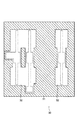
図1は本発明の第1の実施形態に係わるゲート配線パターンの構成を示す平面図である。図1において、符号11はゲート長30nmのゲート部、符号12は幅140nmの連結配線部、符号13はコンタクトパッド部である。
【0015】
図1に示したパターンを従来技術で述べた2重露光によりパターニングすることを考える。2重露光をするために図2に示すレベンソン位相シフト型フォトマスク(第1のフォトマスク)20と,図3に示すトリムマスク30との二つを用いる。なお、トリムマスク(第2のフォトマスク)30はハーフトーン位相シフト型フォトマスクを用いても良い。二つのマスクを用いてマスクを形成した後のエッチング工程において、ゲート電極の周辺のパターンが異なる。図2において、符号21は遮光部、22,23は開口部である。開口部23を透過した光の位相は、開口部22を透過した光の位相と180゜異なる。図3において、符号31は位相シフト部、符号32は開口部である。図1に示したパターンを図2,図3では破線で示している。
【0016】
図4〜図10を用いて、本発明の第1の実施形態に係わる半導体装置の製造方法を説明する。図4,図5は図1のA−A’部の断面図、図6,図7はB−B’部の断面図に相当する。図8,9,10は平面図である。
【0017】
まず、図4(a),図6(a)に示すように、素子領域101及び素子分離領域102を有するSi基板上に熱酸化法によりゲート絶縁膜103を形成した後、ゲート絶縁膜103上にCVD(Chemical Vapor Deposition)法等によりゲート電極材料膜としてのSiGe膜104を堆積する。次に、ゲート電極材料膜の上にCVD法によりTEOS膜(マスク材料膜,ハードマスク材料膜)105、スパッタリング法によりa−Si(アモルファスシリコン)膜(マスク材料膜,ハードマスク材料膜)106を堆積する。次に、a−Si膜106上に反射防止膜(マスク材料膜)107、第1のレジスト膜108を塗布・ベークする。
【0018】
次いで、図4(b),図6(b)に示すように、図2に示したレベンソン位相シフト型マスク20を用いた露光により、第1のレジスト膜108に潜像を形成した後、現像を行って、第1のレジストパターン109を形成する。このハードマスク材料膜としては、TEOS膜及びa−Si膜の他に、TEOS膜、a−Si膜、SiON、Si3N4を単独、若しくは組合わせて用いてもよい。また、下地からの光学的反射防止膜となるAl2O3、SiC、カーボン膜、有機膜を単独、若しくは組合わせて用いてもよい。
【0019】
次に、図4(c),図6(c)に示すように、第1のレジストパターン109をマスクに反射防止膜107をRIEする。
【0020】
図4(d),図6(d)に示すように、第1のレジストパターン109をマスクにa−Si膜106をRIEする。通常RIEはレジストパターンに対して被加工膜の加工後のパターンサイズに変換差がつかないようにするが、この工程においてはわざと小さく加工されるようにRIE条件を調整する。つまりスリミングを行う。これによりゲート部分のパターンをa−Si膜106aを形成する。
【0021】
ここで、a−Si膜106aの幅は、第1のレジストパターン109の幅より細くなり、加工変換差が生じる。通常、加工面積に応じて加工変換差(この場合はスリミングを含む加工変換差)が生じる。第1のレベンソンマスク露光後の加工時のパターン環境は、例えば図8に示すようなものである。図8の場合には、元々のレジスト開口パターンO11に対して開口パターンO12が形成される。開口パターンO12とレジスト開口パターンO11との加工変換差A1はレジスト開口パターンO11の幅D1に応じて変化すると考えて良い。正確には、加工変換差は幅D1だけでなく、図中のレジスト開口パターン縦方向の長さにも依存するが、本例では長さ方向に対する依存性は小さいものと考える。
【0022】
図4(e),図6(e)に示すように、反射防止膜107及び第1のレジストパターン109を剥離する。
図5(f),図7(f)に示すように、加工後のa−Si膜106上に第2の反射防止膜110を形成した後、レジスト剤を塗布・ベークして第2のレジスト膜を形成する。第2のマスク(トリムマスク)を用いた露光により第2のレジスト膜に、露光・現像を行って第2のレジストパターン111を形成する。
【0023】
次に、図5(g),図7(g)に示すように、第2のレジストパターン111をマスクに第2の反射防止膜110及びa−Si膜106をRIEする。RIE後の平面図を図9に示す。図9において、破線で囲まれた領域が第2のレジストパターンが合った領域、点が描画されている領域がRIE後にa−Si膜106が残存する部分である。元々のレジストのエッジE21に対して、a−Si膜106のエッジE22が形成される。エッジE21とエッジE22との加工変換差A2はエッジE21とエッジE23との距離D2に応じて変化すると考えて良い。
【0024】
ここで、第1の露光及び加工においてa−Si膜106は既に加工されており、第2の露光後の加工においては、TEOS膜105が露出している箇所がある。第2の加工は加工されたa−Si膜106をさらに加工し、露出したTEOS膜105は加工されないような条件で行う。さらに、この工程では配線部を形成するが、配線間スペースがレジストパターンに対して加工後a−Siパターンでできる限り大きくならないよう条件を調整する。
【0025】
次に、図5(h),図7(h)に示すように、第2の反射防止膜110及び第2のレジストパターン111を剥離する。
次に、残存するa−Si膜106をマスクにTEOS膜105をRIEし(図5(i),図7(i))、さらにSiGe膜104をRIEする(図5(j),7(j))。ここで、a−Si膜106に形成されたパターンをSiGe膜104に転写する際、加工変換差が生じる。通常、加工変換差は、加工面積に応じて生じる。RIE後の平面図を図10に示す。図10において、破線で囲まれた領域がa−Si膜106があった領域、実線で囲まれている領域がRIE後にSiGe膜104が残存する部分である。元々のレジストのエッジE3a1,E3a1に対して、SiGe膜104のエッジE3a2,E3b2が形成される。エッジE3a1,E3b1とエッジE3a2,E3b2との加工変換差A3a,A3bはエッジE3a1,E3a1とエッジE3a3,E3b3との距離D3a,D3bに応じて変化すると考えて良い。
【0026】
ここでTEOS膜を用いたのは、a−Si膜のRIE時にほとんどエッチングされない、つまり対a−Si膜との選択比を高くとることができエッチング停止膜として機能し、かつSiGe膜のRIE時には同じく対SiGeとの選択比を高くすることができマスク材として機能するためである。
【0027】
最後に、図5(k),7(k)にしめすように、a−Si膜及びTEOS膜を剥離する。
所望のゲート寸法、連結配線部寸法及びコンタクトパッド部の寸法を得るためには、以下に示す補正を行う。ここでいう補正とは、第1、第2のマスク寸法に補正を加えることである。
【0028】
図11を用いてマスクデータの補正方法を説明する。先ず、入力データを用意する(ステップS101)。ここで入力データとは所望のゲートパターンを形成するためのレベンソンマスクの開口部とトリムマスクのパターンを発生させたデータのことである(図12,図13)。図12に示すレベンソン位相シフトマスクデータにおいて、符号42,43が開口領域である。開口領域43の透過光の位相は、開口領域42の透過光の位相と180゜異なる。また、図13に示すトリムマスクデータにおいて、符号52は遮光領域である。この図12及び図13のマスクデータにおいて、開口領域と遮光領域の境界はゲートパターンに接している。
【0029】
ここで、レベンソン位相シフト型マスクを用いて形成されたレジストパターン形成後のエッチング工程時のパターンと、トリムマスクを用いて形成されたレジストパターン形成後のエッチング工程時のパターン環境とが異なる。よって、それぞれのパターン環境に応じて、レベンソン位相シフト型マスク及びトリムマスクに対して補正を加える。
【0030】
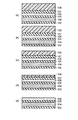
第1のレジストパターンをマスクにした加工時に生じる加工変換差、第2のレジストパターンをマスクにした加工時に生じる加工変換差、及びa−Si膜をマスクにしたSiGe膜の加工時に生じる加工変換差のパターン依存性を図14に示す。図14において、破線は第1のレジストパターンをマスクにして形成されるa−Si膜の加工変換差のパターン依存性を示している。一点鎖線は、a−Si膜をマスクにして形成されるSiGe膜の加工変換差のパターン依存性を示している。二点鎖線は、第2のレジストパターンをマスクにして形成されるa−Si膜の加工変換差のパターン依存性を示している。
【0031】
そこで、第1のレジストパターンをマスクとして用いた加工時に生じる加工変換差を図15に示すような、開口パターンの対向するエッジ間の距離に応じた階段状の補正値、を適用して補正する。a−Si膜をマスクに用いたSiGe膜の加工時に生じる加工変換差を図16に示すような、隣のパターンまでの距離に応じた階段状の補正値、を適用して補正する。第2のレジストパターンをマスクにして形成されるa−Si膜の加工時に生じる加工変換差を図17に示すような、隣のパターンまでの距離に応じた階段状の補正値、を適用して補正する。
【0032】
この補正値を表1、2,3にまとめる。表1は、開口パターンの対向するエッジ間の距離に応じた第1のレジストパターンを補正する階段状の補正値。表2は、a−Si膜をマスクに用いたSiGe膜の加工時に生じる加工変換差を補正する隣接するパターンの距離に応じた補正値。表3は、第2のレジストパターンをマスクにして形成されるa−Si膜の加工時に生じる加工変換差を補正する隣接するパターンの距離に応じた補正値である。
【0033】
【表1】

【表2】
【表3】
なお、表1〜3に示すバイアス量はエッチングを後退させる方向を+としている。
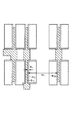
まず、レベンソン位相シフト型マスクを用いて加工された領域のa−Si膜をマスクに用いたSiGe膜の加工時に生じる加工変換差を補正する(ステップS102)。図16及び表2に示す補正テーブルを準備する。補正対象エッジEc1と隣接するゲートパターンのエッジEc3とのスペースDc1を測定する。測定値Dc1と表2のテーブルから補正値B1を決定する。図18に示すように、補正対象エッジEc1を補正値B1後退させ、補正対象エッジEc2を得る。
【0037】
次に、レベンソン位相シフト型マスクをマスクに用いたa−Si膜の加工時に生じる加工変換差を補正する(ステップS103)。図15及び表1に示す補正テーブルを準備し、補正対象エッジEc2と隣接するレベンソンマスクのスペースパターンのエッジEc4との距離(スペース)Dc2を測定する。測定値Dc2と表1のテーブルから補正値B2を決定する。図19に示すように、補正対象エッジEc2を補正値B2後退させ、補正対象エッジEc4を得る。
【0038】
トリムマスクを用いて加工された領域のa−Si膜をマスクに用いたSiGe膜の加工時に生じる加工変換差を補正する(ステップS104)。図16及び表2に示す補正テーブルを準備する。補正対象エッジEc6と隣接するパターンのエッジEc8とのスペースDc1を測定する。測定値Dc1と表2のテーブルから補正値B3を決定する。図20に示すように、補正対象エッジEc6を補正値B3後退させ、補正対象エッジEc7を得る。
【0039】
次に、トリムマスクを用いて形成される第2のレジストパターンをマスクに用いてa−Si膜を加工する時に生じる加工変換差を補正する(ステップS105)。図17及び表3に示す補正テーブルを準備する。補正対象エッジEc7と隣接するパターンのエッジEc10とのスペースDc4を測定する。測定値Dc4と表3のテーブルから補正値B4を決定する。図21に示すように、補正対象エッジEc7を補正値B4後退させ、補正対象エッジEc9を得る。
【0040】
次いで、光近接効果補正を行う(ステップS106)。これは、光近接効果を補正するためのもので、加工変換差の補正とは個別に行った。ここではモデルOPC、すなわち光学シミュレーションを行って、これに基づき各パターンエッジの補正を行った。
【0041】
ゲート寸法の精度を高めるために、光近接補正は個別に補正することが望ましい。但し、加工変換差が小さくゲート寸法の形成精度に許される値であれば同時に、つまりOPCの補正に組み込んで補正しても構わない。また、ここではモデルOPCとしたが、ルールベースOPC、すなわちマスク寸法とウェハ上のレジスト形成寸法との変換差を測定して上述の加工変換差と同様の補正テーブルを準備し、これに応じて補正する方法でも構わない。
【0042】
また、モデルOPC後にマスクとして作成困難なパターン寸法が存在する場合には、これを検出し、マスク値を作成可能なサイズに拡大する処理を加えても良い。
最後に、マスクを作製するための描画データに変換する(ステップS107)。
【0043】
上記の工程後、図示しないが、前記ゲートパターンをマスクに露出したSi基板表面に不純物注入を行い、トランジスタのソース・ドレイン拡散層を形成した後、周知の層間絶縁膜形成、メタル配線工程等を行うことによりMOSトランジスタが完成される。
【0044】
パターン環境が異なる加工変換差のパターン依存性を各々補正することにより、最終的に得られるパターンの寸法精度を向上することができる。
【0045】
本実施例はゲート電極材料パターンの形成に用いた例であるが、この限りではない。
レベンソンマスクを用いた露光工程とトリムマスクを用いたの露光工程の順序は上記と逆でもいい。また、一般にゲート電極はPMOSとNMOSに分類される。両者のゲート電極材料の加工特性が異なる場合には、各々に応じて個別の補正値を適用することが望ましい。つまりここではSiGe膜の加工変換差の補正値を各々個別の値を適用する。
【0046】
(第2の実施形態)
本実施形態では、例えば第1のレジストパターンに対するa−Si膜の加工変換差(以下、第1の加工変換差)のスペース依存性が小さい場合に、二つの補正を一括して行う例を示す。
【0047】
第1のレジストパターンに対するa−Si膜の加工変換差のスペース依存性を図22に示す。ここでスペース依存性が小さく、つまりスペースが小さい場合(密なパターン)と大きい場合(孤立パターン)で加工変換差はほとんど違いがない。
【0048】
この加工変換差の差がゲート寸法の精度(誤差)として許される値の場合には、a−Si膜に対するSiGe膜の加工変換差(以下、第2の加工変換差)のスペース依存性の補正に第1の加工変換差の補正値を加えて補正してもよい。
【0049】
つまり、第1の加工変換差の平均値を1nmとすると、その1nmを第2の加工変換差の補正値にそのまま加えて補正しても良い。
【0050】
例えば第1の加工工程の加工変換差のスペース依存性が小さい場合に、第1、第2の加工工程において生じる加工変換差のパターン依存性を一括して補正することにより、最終的に得られるパターンの寸法精度を向上することができ、かつ処理を短時間で終わらせることができる。
【0051】
なお、本発明は、上記実施形態に限定されるものではなく、実施段階ではその要旨を逸脱しない範囲で種々に変形することが可能である。更に、上記実施形態には種々の段階の発明が含まれており、開示される複数の構成要件における適宜な組み合わせにより種々の発明が抽出され得る。例えば、実施形態に示される全構成要件から幾つかの構成要件が削除されても、発明が解決しようとする課題の欄で述べた課題が解決でき、発明の効果の欄で述べられている効果が得られる場合には、この構成要件が削除された構成が発明として抽出され得る。
【0052】
【発明の効果】
以上説明したように本発明によれば、2重転写法を用いてパターンを形成する際に、所望の寸法のパターンを得ることが出来る。
【図面の簡単な説明】
【図1】第1の実施形態に係わるゲート配線パターンの構成を示す平面図。
【図2】第1の実施形態に係わるレベンソン位相シフト型フォトマスクの構成を示す平面図。
【図3】第1の実施形態に係わるトリムマスクの構成を示す平面図。
【図4】図1に示すゲート配線パターンの製造工程を示す断面図。
【図5】図1に示すゲート配線パターンの製造工程を示す断面図。
【図6】図1に示すゲート配線パターンの製造工程を示す断面図。
【図7】図1に示すゲート配線パターンの製造工程を示す断面図。
【図8】図1に示すゲート配線パターンの製造工程を示す平面図。
【図9】図1に示すゲート配線パターンの製造工程を示す平面図。
【図10】図1に示すゲート配線パターンの製造工程を示す平面図。
【図11】第1の実施形態に係わるマスクの補正方法を示すフローチャート。
【図12】レベンソン位相シフトマスクデータを示す図。
【図13】トリムマスクデータを示す図。
【図14】第1のレジストパターンをマスクにした加工時に生じる加工変換差、第2のレジストパターンをマスクにした加工時に生じる加工変換差、及びa−Si膜をマスクにしたSiGe膜の加工時に生じる加工変換差のパターン依存性をに示す図。
【図15】第1のレジストパターンの開口パターンの対向するエッジ間の距離に応じた階段状の補正値を示す図。
【図16】a−Si膜をマスクに用いたSiGe膜の加工時に生じる加工変換差を補正するための、隣のパターンまでの距離に応じた階段状の補正値を示す特性図。
【図17】第2のレジストパターンをマスクにして形成されるa−Si膜の加工時に生じる加工変換差を補正するための、隣のパターンまでの距離に応じた階段状の補正値を示す特性図。
【図18】a−Si膜をマスクに用いたSiGe膜の加工時に生じる加工変換差を補正するための、レベンソン位相シフト型マスクの補正を説明する図。
【図19】レベンソン位相シフト型マスクをマスクに用いたa−Si膜に生じる加工変換差を補正するための、レベンソン位相シフト型マスクの補正を説明する図。
【図20】a−Si膜をマスクに用いたSiGe膜の加工時に生じる加工変換差を補正するための、トリムマスクの補正を説明する図。
【図21】トリムマスクをマスクに用いたa−Si膜に生じる加工変換差を補正するための、レベンソン位相シフト型マスクの補正を説明する図。
【図22】第1のレジストパターンに対するa−Si膜の加工変換差のスペース依存性を示す図。
【符号の説明】
101…素子領域,102…素子分離領域,103…ゲート絶縁膜,104…膜,105…TEOS膜,106…a−Si膜,107…反射防止膜,108…第1のレジスト膜,109…第1のレジストパターン,110…第2の反射防止膜,111…第2のレジストパターン[0001]
TECHNICAL FIELD OF THE INVENTION
The present invention relates to a method for correcting a photomask used in a method for manufacturing a semiconductor device that forms a semiconductor device using a double transfer method, and a method for manufacturing a semiconductor device using the corrected photomask.
[0002]
[Prior art]
2. Description of the Related Art In recent years, in the manufacture of semiconductor memory devices, higher integration of elements and wirings constituting circuits and finer patterns have been promoted. In the manufacture of an EWS (Engineering Work Station), a RISC processor used as a CPU of a PC (Personal Computer), or the like, a pattern formation with a gate width of a transistor of 100 nm or less is required in 2002.
[0003]
In recent years, there has been proposed a method of forming a gate smaller than a resist pattern in order to form a finer gate (Patent Document 1). The method described in Patent Document 1 is referred to herein as a double transfer method.
[0004]
First, a first resist pattern is formed using a Levenson mask, and the base film is slimmed using the first resist pattern as a mask. Next, after the first resist pattern is peeled off, a resist is applied again, and the trim mask is exposed to form a second resist pattern. Thereafter, the base film is processed without slimming or with a reduced amount of slimming, and finally a gate is formed.
[0005]
Patent Document 1 does not describe how to accurately form an electrode having a desired width.
[0006]
[Patent Document 1]
JP-A-2002-359352 (paragraphs [0032] to [0049], FIGS. 1 to 8)
[0007]
[Problems to be solved by the invention]
There has been no known method for obtaining a pattern having a desired size using the double transfer method.
[0008]
An object of the present invention is to provide a method of correcting a photomask that can obtain a pattern having a desired size by using a double transfer method, and a method of manufacturing a semiconductor device using the corrected photomask.
[0009]
[Means for Solving the Problems]
The present invention is configured as described below to achieve the above object.
[0010]
According to one embodiment of the present invention, there is provided a method of correcting a photomask, comprising: depositing a mask material film on a film to be processed, and transferring a pattern formed on a first photomask onto the mask material film; Forming a mask pattern by processing the mask material film using the first resist pattern as a mask; removing the first resist pattern; and the mask including the mask pattern Forming a second resist pattern onto which a pattern formed on a second photomask is transferred on a material film; and processing the mask material film exposed in an opening of the second resist pattern. Processing the film to be processed using the mask material film pattern as a mask. A method of correcting a mask, comprising: performing a correction on a pattern dimension of a first photomask based on a processing conversion difference depending on a pattern at the time of processing using a first resist pattern as a mask; A method for correcting a photomask, comprising: correcting a pattern size of a photomask based on a processing conversion difference depending on a pattern at the time of etching the film to be processed using the mask pattern as a mask.
[0011]
According to one embodiment of the present invention, there is provided a method of correcting a photomask, comprising: depositing a mask material film on a film to be processed, and transferring a pattern formed on a second photomask onto the mask material film; Forming a mask pattern by processing the mask material film using the second resist pattern as a mask; removing the second resist pattern; and the mask including the mask pattern Forming a first resist pattern onto which a pattern formed on a first photomask is transferred on a material film, and processing the mask material film exposed in an opening of the first resist pattern; Processing the film to be processed using the mask material film pattern as a mask, the method for correcting a photomask used in the method of manufacturing a semiconductor device. Then, the pattern size of the first photomask is corrected based on the processing conversion difference depending on the pattern at the time of processing using the first resist pattern as a mask, and the pattern size of the first photomask is corrected. And performing a correction based on a processing conversion difference depending on a pattern at the time of etching the film to be processed using the mask pattern as a mask. According to one embodiment of the present invention, there is provided a method of manufacturing a semiconductor device, comprising: depositing a mask material film on a film to be processed; and transferring a pattern formed on a first photo film onto the mask material film. Forming a mask pattern by processing the mask material film using the first resist pattern as a mask; removing the first resist pattern; and the mask including the mask pattern Forming a second resist pattern onto which a pattern formed on a second photomask is transferred on a material film; and processing the mask material film exposed in an opening of the second resist pattern. Processing the film to be processed using the mask material film pattern as a mask, wherein the pattern size of the first photomask is Correction based on a processing conversion difference depending on a pattern at the time of processing using the first resist pattern as a mask, and processing dependent on a pattern at the time of etching processing of the second film to be processed using the mask pattern as a mask The correction based on the conversion difference is performed.
[0012]
According to one embodiment of the present invention, there is provided a method of manufacturing a semiconductor device, comprising: depositing a mask material film on a film to be processed; and transferring a pattern formed on a first photo film onto the mask material film. Forming a mask pattern by processing the mask material film using the first resist pattern as a mask; removing the first resist pattern; and the mask including the mask pattern Forming a second resist pattern onto which a pattern formed on a second photomask is transferred on a material film; and processing the mask material film exposed in an opening of the second resist pattern. Processing the film to be processed using the mask material film pattern as a mask, wherein the pattern size of the second photomask is The correction based on the processing conversion difference depending on the pattern at the time of processing using the second resist pattern as a mask, and the processing conversion difference depending on the pattern at the time of etching processing of the film to be processed using the mask pattern as a mask And correction based on the correction is performed.
[0013]
BEST MODE FOR CARRYING OUT THE INVENTION
Embodiments of the present invention will be described below with reference to the drawings.
[0014]
(1st Embodiment)
FIG. 1 is a plan view showing a configuration of a gate wiring pattern according to the first embodiment of the present invention. In FIG. 1,
[0015]
It is assumed that the pattern shown in FIG. 1 is patterned by the double exposure described in the related art. Two double exposures, a Levenson phase shift photomask (first photomask) 20 shown in FIG. 2 and a
[0016]
A method of manufacturing a semiconductor device according to the first embodiment of the present invention will be described with reference to FIGS. 4 and 5 are sectional views taken along the line AA 'of FIG. 1, and FIGS. 6 and 7 are sectional views taken along the line BB' of FIG. 8, 9, and 10 are plan views.
[0017]
First, as shown in FIGS. 4A and 6A, a
[0018]
Next, as shown in FIGS. 4B and 6B, a latent image is formed on the first resist
[0019]
Next, as shown in FIGS. 4C and 6C, the
[0020]
As shown in FIGS. 4D and 6D, the
[0021]
Here, the width of the
[0022]
As shown in FIGS. 4E and 6E, the
As shown in FIGS. 5F and 7F, after forming the
[0023]
Next, as shown in FIGS. 5G and 7G, the
[0024]
Here, the
[0025]
Next, as shown in FIGS. 5H and 7H, the
Next, RIE is performed on the
[0026]
The reason for using the TEOS film here is that the a-Si film is hardly etched at the time of RIE, that is, the selectivity with respect to the a-Si film can be made high, which functions as an etching stop film, and at the time of RIE of the SiGe film. Similarly, it is possible to increase the selectivity with respect to SiGe and to function as a mask material.
[0027]
Finally, as shown in FIGS. 5 (k) and 7 (k), the a-Si film and the TEOS film are peeled off.
In order to obtain desired gate dimensions, connection wiring dimensions, and contact pad dimensions, the following corrections are made. The correction here is to add correction to the first and second mask dimensions.
[0028]
A method of correcting mask data will be described with reference to FIG. First, input data is prepared (step S101). Here, the input data refers to data that generates an opening of a Levenson mask and a pattern of a trim mask for forming a desired gate pattern (FIGS. 12 and 13). In the Levenson phase shift mask data shown in FIG. 12,
[0029]
Here, the pattern environment during the etching step after the formation of the resist pattern formed using the Levenson phase shift mask is different from the pattern environment during the etching step after the formation of the resist pattern formed using the trim mask. Therefore, correction is applied to the Levenson phase shift mask and the trim mask according to each pattern environment.
[0030]
Processing conversion difference generated during processing using the first resist pattern as a mask, processing conversion difference generated during processing using the second resist pattern as a mask, and processing conversion difference generated during processing of a SiGe film using an a-Si film as a mask FIG. 14 shows the pattern dependence. In FIG. 14, the broken line indicates the pattern dependence of the processing conversion difference of the a-Si film formed using the first resist pattern as a mask. The alternate long and short dash line indicates the pattern dependence of the processing conversion difference of the SiGe film formed using the a-Si film as a mask. The two-dot chain line indicates the pattern dependence of the processing conversion difference of the a-Si film formed using the second resist pattern as a mask.
[0031]
Therefore, the processing conversion difference generated at the time of processing using the first resist pattern as a mask is corrected by applying a stepwise correction value according to the distance between opposing edges of the opening pattern as shown in FIG. . The processing conversion difference generated when processing the SiGe film using the a-Si film as a mask is corrected by applying a step-like correction value according to the distance to an adjacent pattern as shown in FIG. By applying a step-like correction value corresponding to the distance to an adjacent pattern as shown in FIG. 17, a processing conversion difference generated when processing an a-Si film formed using the second resist pattern as a mask is applied. to correct.
[0032]
The correction values are summarized in Tables 1, 2, and 3. Table 1 shows a stepwise correction value for correcting the first resist pattern according to the distance between opposing edges of the opening pattern. Table 2 shows correction values according to the distance between adjacent patterns for correcting a processing conversion difference generated when processing an SiGe film using an a-Si film as a mask. Table 3 shows correction values according to the distance between adjacent patterns for correcting a processing conversion difference generated when processing an a-Si film formed using the second resist pattern as a mask.
[0033]
[Table 1]
[Table 2]
[Table 3]
In the bias amounts shown in Tables 1 to 3, the direction in which the etching is retreated is indicated by +.
First, a processing conversion difference generated when processing an SiGe film using an a-Si film in a region processed using a Levenson phase shift mask as a mask is corrected (step S102). A correction table shown in FIG. 16 and Table 2 is prepared. Measuring the space Dc 1 between the correction target edge Ec 1 and edge Ec 3 adjacent gate patterns. Determining a correction value B 1 from the measured value Dc 1 and Table 2 Table. As shown in FIG. 18, the correction value B 1 is retracted the correction target edges Ec 1, to obtain a corrected edge Ec 2.
[0037]
Next, a processing conversion difference generated when processing the a-Si film using the Levenson phase shift mask as a mask is corrected (step S103). Prepare the correction table shown in FIG. 15 and Table 1, to measure the correct distance of the target edge Ec 2 and edge Ec 4 of space pattern of adjacent Levenson mask (space) Dc 2. Determining a correction value B 2 from the measured values Dc 2 and Table 1 table. As shown in FIG. 19, the correction value B 2 is retracted correction target edge Ec 2, to obtain a corrected edge Ec 4.
[0038]
The processing conversion difference generated when processing the SiGe film using the a-Si film in the region processed using the trim mask as a mask is corrected (step S104). A correction table shown in FIG. 16 and Table 2 is prepared. Measuring the space Dc 1 between the correction target edge Ec 6 and edge Ec 8 of adjacent patterns. Determining a correction value B 3 from the measured value Dc 1 and Table 2 Table. As shown in FIG. 20, the correction target edge Ec 6 is retracted by the correction value B 3 to obtain the correction target edge Ec 7 .
[0039]
Next, a processing conversion difference generated when processing the a-Si film using the second resist pattern formed using the trim mask as a mask is corrected (step S105). A correction table shown in FIG. 17 and Table 3 is prepared. Measuring the space Dc 4 between the correction target edge Ec 7 and edge Ec 10 of adjacent patterns. Determining a correction value B 4 from measurements Dc 4 and Table 3 Table. As shown in FIG. 21, the correction value B 4 retracts the correction target edge Ec 7, to obtain a corrected edge Ec 9.
[0040]
Next, optical proximity effect correction is performed (step S106). This is for correcting the optical proximity effect, and was performed separately from the correction for the processing conversion difference. Here, model OPC, that is, optical simulation was performed, and based on this, each pattern edge was corrected.
[0041]
It is desirable to individually correct the optical proximity correction in order to increase the accuracy of the gate dimension. However, as long as the processing conversion difference is small and the value is allowed for the formation accuracy of the gate dimension, the correction may be performed simultaneously, that is, incorporated into the OPC correction. Although the model OPC is used here, a rule-based OPC, that is, a conversion difference between a mask dimension and a resist formation dimension on a wafer is measured to prepare a correction table similar to the processing conversion difference described above. A correction method may be used.
[0042]
If there is a pattern dimension that is difficult to create as a mask after the model OPC, a process of detecting this and expanding the mask value to a size that can be created may be added.
Finally, the data is converted into drawing data for producing a mask (step S107).
[0043]
After the above process, although not shown, impurities are implanted into the surface of the Si substrate exposed using the gate pattern as a mask to form source / drain diffusion layers of the transistor. By doing so, the MOS transistor is completed.
[0044]
The dimensional accuracy of the finally obtained pattern can be improved by correcting the pattern dependence of the processing conversion difference having different pattern environments.
[0045]
The present embodiment is an example used for forming a gate electrode material pattern, but is not limited to this.
The order of the exposure step using the Levenson mask and the exposure step using the trim mask may be reversed. Generally, gate electrodes are classified into PMOS and NMOS. When the processing characteristics of the two gate electrode materials are different, it is desirable to apply individual correction values to each of them. That is, here, individual values are applied to the correction values of the processing conversion difference of the SiGe film.
[0046]
(Second embodiment)
In the present embodiment, for example, when the space dependence of the processing conversion difference of the a-Si film with respect to the first resist pattern (hereinafter, the first processing conversion difference) is small, two corrections are collectively performed. .
[0047]
FIG. 22 shows the space dependence of the processing conversion difference of the a-Si film with respect to the first resist pattern. Here, there is almost no difference between the processing conversions when the space dependency is small, that is, when the space is small (dense pattern) and when the space is large (isolated pattern).
[0048]
If the difference between the processing conversions is a value allowed as the accuracy (error) of the gate dimension, the correction of the space dependence of the processing conversion difference of the SiGe film with respect to the a-Si film (hereinafter, the second processing conversion difference). May be corrected by adding a correction value of the first processing conversion difference to the correction value.
[0049]
That is, assuming that the average value of the first processing conversion difference is 1 nm, the correction may be performed by adding the 1 nm as it is to the correction value of the second processing conversion difference.
[0050]
For example, when the space dependency of the processing conversion difference in the first processing step is small, the pattern dependency of the processing conversion difference generated in the first and second processing steps is collectively corrected, thereby finally being obtained. The dimensional accuracy of the pattern can be improved, and the processing can be completed in a short time.
[0051]
Note that the present invention is not limited to the above-described embodiment, and can be variously modified in an implementation stage without departing from the gist of the invention. Further, the above embodiments include inventions at various stages, and various inventions can be extracted by appropriately combining a plurality of disclosed constituent elements. For example, even if some components are deleted from all the components shown in the embodiment, the problem described in the column of the problem to be solved by the invention can be solved, and the effects described in the column of the effect of the invention can be solved. Is obtained, a configuration from which this configuration requirement is deleted can be extracted as an invention.
[0052]
【The invention's effect】
As described above, according to the present invention, a pattern having a desired size can be obtained when a pattern is formed using the double transfer method.
[Brief description of the drawings]
FIG. 1 is a plan view showing a configuration of a gate wiring pattern according to a first embodiment.
FIG. 2 is a plan view showing a configuration of a Levenson phase shift photomask according to the first embodiment.
FIG. 3 is a plan view showing a configuration of a trim mask according to the first embodiment.
FIG. 4 is a sectional view showing a manufacturing step of the gate wiring pattern shown in FIG. 1;
FIG. 5 is a sectional view showing a step of manufacturing the gate wiring pattern shown in FIG. 1;
FIG. 6 is a sectional view showing a manufacturing step of the gate wiring pattern shown in FIG. 1;
FIG. 7 is a sectional view showing the manufacturing process of the gate wiring pattern shown in FIG. 1;
FIG. 8 is a plan view showing a step of manufacturing the gate wiring pattern shown in FIG.
9 is a plan view showing a step of manufacturing the gate wiring pattern shown in FIG.
10 is a plan view showing a step of manufacturing the gate wiring pattern shown in FIG.
FIG. 11 is a flowchart illustrating a mask correction method according to the first embodiment.
FIG. 12 is a diagram showing Levenson phase shift mask data.
FIG. 13 is a view showing trim mask data.
FIG. 14 shows a processing conversion difference generated when processing using the first resist pattern as a mask, a processing conversion difference generated when processing using the second resist pattern as a mask, and a processing conversion difference generated when processing an SiGe film using an a-Si film as a mask. The figure which shows the pattern dependence of the processing conversion difference which arises.
FIG. 15 is a diagram showing a step-like correction value according to a distance between opposing edges of an opening pattern of a first resist pattern.
FIG. 16 is a characteristic diagram showing a stepwise correction value according to a distance to an adjacent pattern for correcting a processing conversion difference generated when processing an SiGe film using an a-Si film as a mask.
FIG. 17 is a characteristic showing a step-like correction value according to a distance to an adjacent pattern for correcting a processing conversion difference generated when processing an a-Si film formed using a second resist pattern as a mask. FIG.
FIG. 18 is a view for explaining correction of a Levenson phase shift mask for correcting a processing conversion difference generated when processing an SiGe film using an a-Si film as a mask.
FIG. 19 is a view for explaining correction of a Levenson phase shift mask for correcting a processing conversion difference generated in an a-Si film using a Levenson phase shift mask as a mask.
FIG. 20 is a diagram for explaining trim mask correction for correcting a processing conversion difference generated when processing an SiGe film using an a-Si film as a mask.
FIG. 21 is a view for explaining correction of a Levenson phase shift type mask for correcting a processing conversion difference generated in an a-Si film using a trim mask as a mask.
FIG. 22 is a diagram showing the space dependence of the processing conversion difference of the a-Si film with respect to the first resist pattern.
[Explanation of symbols]
101 element region, 102 element isolation region, 103 gate insulating film, 104 film, 105 TEOS film, 106 a-Si film, 107 antireflection film, 108 first resist film, 109 1 resist pattern, 110... Second antireflection film, 111... Second resist pattern
Claims (15)
前記第1のレジストパターンをマスクに前記マスク材料膜を加工してマスクパターンを形成する工程と、
前記第1のレジストパターンを剥離する工程と、
前記マスクパターンを含む前記マスク材料膜上に第2のフォトマスクに形成されたパターンが転写された第2のレジストパターンを形成する工程と、
前記第2のレジストパターンの開口内に露出した前記マスク材料膜を加工する工程と、
前記マスク材料膜パターンをマスクに前記被加工膜を加工する工程とを含む半導体装置の製造方法に用いられるフォトマスクを補正するフォトマスクの補正方法であって、
第1のフォトマスクのパターン寸法に対して、第1のレジストパターンをマスクに用いた加工時のパターンに依存する加工変換差に基づく補正を行い、
前記第1のフォトマスクのパターン寸法に対して、前記マスクパターンをマスクに用いた前記被加工膜のエッチング加工時のパターンに依存する加工変換差に基づく補正を行うことを特徴とするフォトマスクの補正方法。Depositing a mask material film on the film to be processed, and forming a first resist pattern on which the pattern formed on the first photomask is transferred, on the mask material film;
Processing the mask material film using the first resist pattern as a mask to form a mask pattern;
Stripping the first resist pattern;
Forming a second resist pattern on which the pattern formed on the second photomask is transferred on the mask material film including the mask pattern;
Processing the mask material film exposed in the opening of the second resist pattern;
Processing the film to be processed using the mask material film pattern as a mask, a method of correcting a photomask used in a method of manufacturing a semiconductor device, the method comprising:
A correction based on a processing conversion difference depending on a pattern at the time of processing using the first resist pattern as a mask is performed on a pattern dimension of the first photomask,
The correction of a pattern dimension of the first photomask is performed based on a processing conversion difference depending on a pattern at the time of etching processing of the film to be processed using the mask pattern as a mask. Correction method.
前記第2のレジストパターンをマスクに前記マスク材料膜を加工してマスクパターンを形成する工程と、
前記第2のレジストパターンを剥離する工程と、
前記マスクパターンを含む前記マスク材料膜上に第1のフォトマスクに形成されたパターンが転写された第1のレジストパターンを形成する工程と、
前記第1のレジストパターンの開口内に露出した前記マスク材料膜を加工する工程と、
前記マスク材料膜パターンをマスクに前記被加工膜を加工する工程とを含む半導体装置の製造方法に用いられるフォトマスクの補正方法において、
第1のフォトマスクのパターン寸法に対して、第1のレジストパターンをマスクに用いた加工時のパターンに依存する加工変換差に基づく補正を行い、
第1のフォトマスクのパターン寸法に対して、前記マスクパターンをマスクに用いた前記被加工膜のエッチング加工時のパターンに依存する加工変換差に基づく補正を行うことを特徴とするフォトマスクの補正方法。Depositing a mask material film on the film to be processed, and forming a second resist pattern on which the pattern formed on the second photomask is transferred, on the mask material film;
Processing the mask material film using the second resist pattern as a mask to form a mask pattern;
Removing the second resist pattern;
Forming a first resist pattern on which a pattern formed on a first photomask is transferred on the mask material film including the mask pattern;
Processing the mask material film exposed in the opening of the first resist pattern;
Processing the film to be processed using the mask material film pattern as a mask.
A correction based on a processing conversion difference depending on a pattern at the time of processing using the first resist pattern as a mask is performed on a pattern dimension of the first photomask,
Correcting the pattern dimension of the first photomask based on a processing conversion difference depending on a pattern at the time of etching the film to be processed using the mask pattern as a mask; Method.
前記第1のレジストパターンをマスクに用いた前記マスク材料膜の加工時、前記第1のレジストパターンの隣接する一対の開口に挟まれた前記マスク材料膜部分を細らせることを特徴とする請求項1又は2に記載のフォトマスクの補正方法。A first resist pattern having a pair of adjacent openings for exposing a selected region of the mask material film, and covering a non-selected region;
When the mask material film is processed using the first resist pattern as a mask, a portion of the mask material film sandwiched between a pair of adjacent openings of the first resist pattern is narrowed. Item 3. The method for correcting a photomask according to Item 1 or 2.
第2のフォトマスクのパターン寸法に対して、前記マスクパターンをマスクに用いた前記被加工膜のエッチング加工時のパターンに依存する加工変換差に基づく補正を行うことを特徴とする請求項1〜3の何れかに記載のフォトマスクの補正方法。A correction based on a processing conversion difference depending on a pattern at the time of processing using the second resist pattern as a mask is performed on a pattern dimension of the second photomask,
2. The method according to claim 1, wherein the pattern size of the second photomask is corrected based on a processing conversion difference depending on a pattern at the time of etching the film to be processed using the mask pattern as a mask. 3. The method for correcting a photomask according to any one of 3.
前記第1のレジストパターンをマスクに前記マスク材料膜を加工してマスクパターンを形成する工程と、
前記第1のレジストパターンを剥離する工程と、
前記マスクパターンを含む前記マスク材料膜上に第2のフォトマスクに形成されたパターンが転写された第2のレジストパターンを形成する工程と、
前記第2のレジストパターンの開口内に露出した前記マスク材料膜を加工する工程と、
前記マスク材料膜パターンをマスクに前記被加工膜を加工する工程とを含む半導体装置の製造方法において、
第1のフォトマスクのパターン寸法は、第1のレジストパターンをマスクに用いた加工時のパターンに依存する加工変換差に基づく補正と、前記マスクパターンをマスクに用いた前記被加工膜のエッチング加工時のパターンに依存する加工変換差に基づく補正とが行われていることを特徴とする半導体装置の製造方法。Depositing a mask material film on the film to be processed, and forming a first resist pattern on which the pattern formed on the first photomask is transferred, on the mask material film;
Processing the mask material film using the first resist pattern as a mask to form a mask pattern;
Stripping the first resist pattern;
Forming a second resist pattern on which the pattern formed on the second photomask is transferred on the mask material film including the mask pattern;
Processing the mask material film exposed in the opening of the second resist pattern;
Processing the film to be processed using the mask material film pattern as a mask.
The pattern size of the first photomask is corrected based on a processing conversion difference depending on a pattern at the time of processing using the first resist pattern as a mask, and etching processing of the film to be processed using the mask pattern as a mask A method of manufacturing a semiconductor device, wherein correction based on a processing conversion difference depending on a time pattern is performed.
前記第2のレジストパターンをマスクに前記マスク材料膜を加工してマスクパターンを形成する工程と、
前記第2のレジストパターンを剥離する工程と、
前記マスクパターンを含む前記マスク材料膜上に第1のフォトマスクに形成されたパターンが転写された第1のレジストパターンを形成する工程と、
前記第1のレジストパターンの開口内に露出した前記マスク材料膜を加工する工程と、
前記マスク材料膜パターンをマスクに前記被加工膜を加工する工程とを含む半導体装置の製造方法において、
第1のフォトマスクのパターン寸法は、第1のレジストパターンをマスクに用いた加工時のパターンに依存する加工変換差に基づく補正と、前記マスクパターンをマスクに用いた前記被加工膜のエッチング加工時のパターンに依存する加工変換差に基づく補正とが行われていることを特徴とする半導体装置の製造方法。Depositing a mask material film on the film to be processed, and forming a second resist pattern on which the pattern formed on the second photomask is transferred, on the mask material film;
Processing the mask material film using the second resist pattern as a mask to form a mask pattern;
Removing the second resist pattern;
Forming a first resist pattern on which a pattern formed on a first photomask is transferred on the mask material film including the mask pattern;
Processing the mask material film exposed in the opening of the first resist pattern;
Processing the film to be processed using the mask material film pattern as a mask.
The pattern size of the first photomask is corrected based on a processing conversion difference depending on a pattern at the time of processing using the first resist pattern as a mask, and etching processing of the film to be processed using the mask pattern as a mask A method of manufacturing a semiconductor device, wherein correction based on a processing conversion difference depending on a time pattern is performed.
前記第1のレジストパターンをマスクに用いた前記マスク材料膜の加工時、前記第1のレジストパターンの隣接する一対の開口に挟まれた前記マスク材料膜部分を細らせることを特徴とする請求項7又は8に記載の半導体装置の製造方法。A first resist pattern having a pair of adjacent openings for exposing a selected region of the mask material film, and covering a non-selected region;
When the mask material film is processed using the first resist pattern as a mask, a portion of the mask material film sandwiched between a pair of adjacent openings of the first resist pattern is narrowed. Item 9. The method for manufacturing a semiconductor device according to item 7 or 8.
Priority Applications (3)
| Application Number | Priority Date | Filing Date | Title |
|---|---|---|---|
| JP2003161038A JP2004363390A (en) | 2003-06-05 | 2003-06-05 | Method of correcting photomask, and method of manufacturing of semiconductor device |
| US10/860,138 US7399557B2 (en) | 2003-06-05 | 2004-06-04 | Photomask correcting method and manufacturing method of semiconductor device |
| US12/216,051 US7670755B2 (en) | 2003-06-05 | 2008-06-27 | Photomask correcting method and manufacturing method of semiconductor device |
Applications Claiming Priority (1)
| Application Number | Priority Date | Filing Date | Title |
|---|---|---|---|
| JP2003161038A JP2004363390A (en) | 2003-06-05 | 2003-06-05 | Method of correcting photomask, and method of manufacturing of semiconductor device |
Publications (1)
| Publication Number | Publication Date |
|---|---|
| JP2004363390A true JP2004363390A (en) | 2004-12-24 |
Family
ID=33508593
Family Applications (1)
| Application Number | Title | Priority Date | Filing Date |
|---|---|---|---|
| JP2003161038A Pending JP2004363390A (en) | 2003-06-05 | 2003-06-05 | Method of correcting photomask, and method of manufacturing of semiconductor device |
Country Status (2)
| Country | Link |
|---|---|
| US (2) | US7399557B2 (en) |
| JP (1) | JP2004363390A (en) |
Cited By (6)
| Publication number | Priority date | Publication date | Assignee | Title |
|---|---|---|---|---|
| JP2007149768A (en) * | 2005-11-24 | 2007-06-14 | Nec Electronics Corp | Method of manufacturing semiconductor device |
| JP2007165704A (en) * | 2005-12-15 | 2007-06-28 | Renesas Technology Corp | Pattern forming method, and manufacturing method for levenson type mask |
| JP2008500727A (en) * | 2004-05-25 | 2008-01-10 | フリースケール セミコンダクター インコーポレイテッド | Separate complementary mask pattern transfer method |
| JP2008083391A (en) * | 2006-09-27 | 2008-04-10 | Toshiba Microelectronics Corp | Multiple exposure photomask and its layout method, method of manufacturing semiconductor device using multiple exposure photomask |
| JP2009080349A (en) * | 2007-09-26 | 2009-04-16 | Toshiba Corp | Method of predicting dimensional conversion difference, method of manufacturing photomask, method of manufacturing electronic part, and program of predicting dimensional conversion difference |
| US7638244B2 (en) | 2004-02-16 | 2009-12-29 | Kabushiki Kaisha Toshiba | Method of correcting mask data, method of manufacturing a mask and method of manufacturing a semiconductor device |
Families Citing this family (7)
| Publication number | Priority date | Publication date | Assignee | Title |
|---|---|---|---|---|
| US20060257795A1 (en) * | 2005-05-16 | 2006-11-16 | Benjamin Szu-Min Lin | Method for forming composite pattern including different types of patterns |
| US7774739B2 (en) * | 2006-11-30 | 2010-08-10 | Texas Instruments Incorporated | Methods for adjusting shifter width of an alternating phase shifter having variable width |
| JP4384199B2 (en) * | 2007-04-04 | 2009-12-16 | 株式会社東芝 | Manufacturing method of semiconductor device |
| KR100983711B1 (en) * | 2008-08-29 | 2010-09-24 | 주식회사 하이닉스반도체 | Method for forming semiconductor device |
| KR101622586B1 (en) * | 2010-03-31 | 2016-05-19 | 후지필름 가부시키가이샤 | Conductive film |
| CN105565260B (en) * | 2016-01-29 | 2018-06-26 | 中国科学院微电子研究所 | The method that Self-Assembling of Block Copolymer manufactures nanostructured |
| CN113380701B (en) * | 2021-05-28 | 2023-03-21 | 惠科股份有限公司 | Manufacturing method of thin film transistor and mask |
Family Cites Families (7)
| Publication number | Priority date | Publication date | Assignee | Title |
|---|---|---|---|---|
| JP4131880B2 (en) | 1997-07-31 | 2008-08-13 | 株式会社東芝 | Mask data creation method and mask data creation apparatus |
| JP3895851B2 (en) | 1997-12-09 | 2007-03-22 | 株式会社東芝 | Mask pattern correction method |
| JP4580529B2 (en) * | 2000-09-26 | 2010-11-17 | 大日本印刷株式会社 | Semiconductor circuit design pattern data correction method, photomask using corrected design pattern data, photomask inspection method, and photomask inspection pattern data preparation method |
| JP4014891B2 (en) | 2001-03-29 | 2007-11-28 | 株式会社東芝 | Manufacturing method of semiconductor device |
| JP2002311563A (en) | 2001-04-17 | 2002-10-23 | Sony Corp | Device and method for generating correction table, device and method for generating mask pattern for correction table, device and method for generating mask pattern for fine working, and method for forming fine working pattern |
| JP4691840B2 (en) | 2001-07-05 | 2011-06-01 | ソニー株式会社 | Mask pattern generation method and photomask |
| JP2003168640A (en) * | 2001-12-03 | 2003-06-13 | Hitachi Ltd | Method of manufacturing semiconductor device |
-
2003
- 2003-06-05 JP JP2003161038A patent/JP2004363390A/en active Pending
-
2004
- 2004-06-04 US US10/860,138 patent/US7399557B2/en not_active Expired - Fee Related
-
2008
- 2008-06-27 US US12/216,051 patent/US7670755B2/en not_active Expired - Fee Related
Cited By (8)
| Publication number | Priority date | Publication date | Assignee | Title |
|---|---|---|---|---|
| US7638244B2 (en) | 2004-02-16 | 2009-12-29 | Kabushiki Kaisha Toshiba | Method of correcting mask data, method of manufacturing a mask and method of manufacturing a semiconductor device |
| JP2008500727A (en) * | 2004-05-25 | 2008-01-10 | フリースケール セミコンダクター インコーポレイテッド | Separate complementary mask pattern transfer method |
| JP2007149768A (en) * | 2005-11-24 | 2007-06-14 | Nec Electronics Corp | Method of manufacturing semiconductor device |
| JP2007165704A (en) * | 2005-12-15 | 2007-06-28 | Renesas Technology Corp | Pattern forming method, and manufacturing method for levenson type mask |
| JP2008083391A (en) * | 2006-09-27 | 2008-04-10 | Toshiba Microelectronics Corp | Multiple exposure photomask and its layout method, method of manufacturing semiconductor device using multiple exposure photomask |
| JP2009080349A (en) * | 2007-09-26 | 2009-04-16 | Toshiba Corp | Method of predicting dimensional conversion difference, method of manufacturing photomask, method of manufacturing electronic part, and program of predicting dimensional conversion difference |
| KR101046494B1 (en) | 2007-09-26 | 2011-07-04 | 가부시끼가이샤 도시바 | Dimensional conversion difference prediction method, photomask manufacturing method, electronic component manufacturing method, and recording medium |
| US8171434B2 (en) | 2007-09-26 | 2012-05-01 | Kabushiki Kaisha Toshiba | Method for dimension conversion difference prediction, method for manufacturing photomask, method for manufacturing electronic component, and program for dimension conversion difference prediction |
Also Published As
| Publication number | Publication date |
|---|---|
| US7399557B2 (en) | 2008-07-15 |
| US20040253525A1 (en) | 2004-12-16 |
| US20080292992A1 (en) | 2008-11-27 |
| US7670755B2 (en) | 2010-03-02 |
Similar Documents
| Publication | Publication Date | Title |
|---|---|---|
| US7569309B2 (en) | Gate critical dimension variation by use of ghost features | |
| US7670755B2 (en) | Photomask correcting method and manufacturing method of semiconductor device | |
| US7739651B2 (en) | Method and apparatus to determine if a pattern is robustly manufacturable | |
| US7638244B2 (en) | Method of correcting mask data, method of manufacturing a mask and method of manufacturing a semiconductor device | |
| US7737016B2 (en) | Two-print two-etch method for enhancement of CD control using ghost poly | |
| US9502306B2 (en) | Pattern formation method that includes partially removing line and space pattern | |
| US9274413B2 (en) | Method for forming layout pattern | |
| US7807343B2 (en) | EDA methodology for extending ghost feature beyond notched active to improve adjacent gate CD control using a two-print-two-etch approach | |
| US7910289B2 (en) | Use of dual mask processing of different composition such as inorganic/organic to enable a single poly etch using a two-print-two-etch approach | |
| JP3492526B2 (en) | Method for characterizing electrical characteristics of MOSFET | |
| JP4874149B2 (en) | Mask pattern correction method and semiconductor device manufacturing method | |
| US7818711B2 (en) | System and method for making photomasks | |
| JP3895851B2 (en) | Mask pattern correction method | |
| US9122835B2 (en) | Method for generating layout of photomask | |
| JP2010211046A (en) | Method and program for verifying pattern | |
| KR20090040614A (en) | Method for fabricating halftone phase shift mask | |
| JP5169575B2 (en) | Photomask pattern creation method | |
| US20080076047A1 (en) | Method of forming image contour for predicting semiconductor device pattern | |
| US9761460B1 (en) | Method of fabricating semiconductor structure | |
| JP2006189576A (en) | Photomask, method for manufacturing the same, and method for manufacturing electronic device | |
| KR0137737B1 (en) | Fabrication method of semiconductor device | |
| KR100815958B1 (en) | Bias Correction Method of Semiconductor Device | |
| JP2004341158A (en) | Mask for exposure, optical proximity effect correction apparatus, optical proximity effect correction method, method for manufacturing semiconductor device, and optical proximity effect correction program | |
| JP4372140B2 (en) | Mask pattern correction system for semiconductor device | |
| JP2009278055A (en) | Exposure time determining method, mask creating method, and semiconductor manufacturing method |
Legal Events
| Date | Code | Title | Description |
|---|---|---|---|
| A977 | Report on retrieval |
Free format text: JAPANESE INTERMEDIATE CODE: A971007 Effective date: 20060223 |
|
| A131 | Notification of reasons for refusal |
Free format text: JAPANESE INTERMEDIATE CODE: A131 Effective date: 20070227 |
|
| A521 | Written amendment |
Free format text: JAPANESE INTERMEDIATE CODE: A523 Effective date: 20070501 |
|
| A02 | Decision of refusal |
Free format text: JAPANESE INTERMEDIATE CODE: A02 Effective date: 20070626 |