【0001】
【発明の属する技術分野】
この発明は、車載電子装置の電源制御装置に係り、詳しくはエミッタフォロワ型の定電圧電源回路のバイアス電流を切り替えることで、待機時に定電圧電源回路で消費される電力を低減するようにした車載電子装置の電源制御回路に関する。
【0002】
【従来の技術】
ECU(マイコン)に定電圧電源を供給する定電圧回路(電圧変換器)の前段に電源スイッチ回路を設け、ECU(マイコン)が動作を停止しているときには電源スイッチ回路をオフ(非給電)状態にすることで、ECU(マイコン)への電源供給を遮断し、これにより暗電流をゼロにして省電力化を図ることは、従来から知られている(特許文献1および4参照)。
【0003】
定電圧回路の出力電圧を直接CPUに供給するとともに、定電圧回路の出力側とCPUの周辺回路との間に電源の供給を制御するスイッチ回路を介設し、CPUはイグニッションスイッチがオフされるとスイッチ回路を導通状態に保持した状態で所定の処理を行なった後に、スイッチ回路をオフ(非導通)状態に制御して、CPUの周辺回路への給電を遮断し、これにより待機時の消費電流を低減するようにした車両用表示装置は、従来から知られている(特許文献2参照。)
NPN型トランジスタのコレクタにバッテリ正極側電源(B+)を供給し、ベースとバッテリ負極側電源(B−)またはグランド(接地電位)との間に定電圧(ツェナー)ダイオードを接続し、コレクタとベースとの間にバイアス抵抗を接続した回路構成とし、定電圧(ツェナー)ダイオードの降伏電圧(ツェナー電圧)に基づいて設定される定電圧をエミッタ側から出力するようにしたエミッタフォロワ型の定電圧回路は、従来から知られている(例えば、特許文献3および5参照)。なお、このエミッタフォロワ型の定電圧回路の出力電圧VCCは、定電圧ダイオードの降伏電圧(ツェナー電圧)をVZDとし、NPN型トランジスタのベース・エミッタ間電圧をVBEとすると、VCC=VZD−VBEとなる。
【0004】
エミッタフォロワ型の定電圧回路を構成するNPN型トランジスタのコレクタとベースの間にスイッチ回路とバイアス抵抗との直列回路を接続し、CPUはイグニッションスイッチがオフにされたことを検出すると、所定の処理(例えばメータ指針の帰零処置等)を行なった後に、スイッチ回路をオフにすることで定電圧回路の出力を停止させてCPUへの給電を遮断し、これによりCPUの無駄な電力消費を無くすようにした車両用計器の駆動装置は、従来から知られている(特許文献4参照)。
【0005】
エミッタフォロワ型の定電圧回路を構成するNPN型トランジスタのコレクタとベースの間に第1のバイアス抵抗を接続するとともに、スイッチ回路と第2のバイアス抵抗との直列回路を第1のバイアス抵抗と並列に接続し、モータ駆動時(負荷電流が大の時)にはスイッチ回路をオン(導通状態)に制御することで、実質的にバイアス抵抗の抵抗値を減少させ、これにより定電圧回路の出力電流を大きくし、モータ非駆動時(負荷電流が小の時)にはスイッチ回路をオフ(非導通状態)に制御することで、実質的にバイアス抵抗の抵抗値を大きくして、バイアス電流を減少させ、これにより電源電池の消耗を少なくするようにした時計用定電圧回路は、従来から知られている(特許文献5参照)。
【0006】
【特許文献1】
特開2002−304240号公報
【特許文献2】
特開平11−255047号公報
【特許文献3】
特開平11−85293号公報(図16)
【特許文献4】
特開2002−90185号公報
【特許文献5】
実開平5−59386号公報(実用新案登録請求の範囲および図1)
【0007】
【発明が解決しようとする課題】
近年、車両(自動2輪車等を含む)には種々の電子装置が搭載されている。これらの電子装置は、CPU(マイコン)を備えたものが多い。車両に搭載される電子装置には、イグニッションスイッチがオフされた状態で、(1)動作する必要がないもの(すなわち、電源供給を遮断してよいもの)と、(2)所定の処理を行なった後に動作を停止するもの(すなわち、所定時間後に電源供給を遮断してよいもの)と、(3)動作を継続する必要があるもの(すなわち、電源供給が必要なもの)とがある。動作を継続する必要があるものとして、時計装置または時計装置内の計時部、車両の盗難を監視する装置等がある。
【0008】
単一の定電圧電源回路から電源供給を遮断してもよい電子装置と常時給電が必要な電子装置との双方に電源供給する場合には、定電圧電源回路の前段に電源スイッチ回路を設けることはできない。
【0009】
そこで、単一の定電圧電源回路から複数の電子装置に定電圧化された電源を供給する場合、(1)イグニッションスイッチがオフの状態では電源供給を遮断してよい電子装置に対しては、定電圧電源回路の出力側と電子装置との間にスイッチ回路を設け、このスイッチ回路をイグニッションスイッチがオフされた際に直ちに非導通状態に制御することで電子装置への給電を停止させることができ、(2)イグニッションスイッチがオフされた時点から所定時間経過後に電源供給を遮断してよい電子装置に対しては、定電圧電源回路の出力側と電子装置との間にスイッチ回路を設け、このスイッチ回路の導通状態を電子装置側の出力によって所定時間保持することで、イグニッションスイッチがオフされた時点から所定時間経過後に電子装置への給電を停止させることができ、(3)時計装置等の常時電源供給を必要とする電子装置に対して定電圧電源回路の出力を直接供給することで、電源を常時供給することができる。このように、電子装置毎に電源供給を遮断することで、不要な電力消費をなくすことができる。
【0010】
しかしながら、NPN型トランジスタのコレクタに正極側バッテリ電源(B+)を供給し、ベースとグランド(接地電位,負極側バッテリ電源(B−))との間に定電圧(ツェナー)ダイオードを接続し、コレクタとベースとの間にバイアス抵抗を接続する構成とし、エミッタ側から定電圧ダイオードの降伏電圧(ツェナー)に基づいて設定される定電圧を出力するようにしたエミッタフォロワ型の定電圧電源回路を用いた場合、以下の課題が生ずる。
【0011】
定電圧電源回路の最大出力電流(すなわち、イグニッションスイッチがオン状態で、この定電圧電源回路から給電を受ける全ての電子装置が動作している状態での電流の最大値)に基づいてバイアス抵抗の値が設定されているため、時計装置等の常時電源供給を必要とする電子装置に対してのみ電源を供給する状態では、バイアス抵抗を介して定電圧ダイオードに不要なバイアス電流が流れており、定電圧電源回路内で無駄な電力を消費している。
【0012】
この発明はこのような課題を解決するためなされたもので、定電圧電源回路から負荷(電子装置)へ供給する電流が少ない待機状態では、定電圧電源回路のバイアス電流を低減することで、定電圧電源回路内での不要な電力消費なくすようにした車載電子装置の電源制御回路を提供することを目的とする。
【0013】
【課題を解決するための手段】
前記課題を解決するためこの発明に係る車載電子装置の電源制御回路は、NPN型のトランジスタのコレクタ側をバッテリの正極側電源の入力端子とし、トランジスタのエミッタ側を定電圧出力端子とし、トランジスタのベースとバッテリの負極側(グランド)との間に定電圧回路を接続し、トランジスタのコレクタとベースとの間にトランジスタのベースおよび定電圧回路に供給するバイアス電流の値を少なくとも2段階に切り替えるバイアス電流切替回路を接続してなるエミッタフォロワ型の定電圧電源回路と、この定電圧電源回路の定電圧出力端子と電子装置の電源端子との間に介設されて電子装置への電源供給を制御する電源スイッチ回路と、イグニッションスイッチがオン状態であるとき及び電子装置から電源供給保持信号が供給されているときは、バイアス電流切替回路をバイアス電流が大の状態に切り替えるとともに電源スイッチ回路を導通状態に制御し、イグニッションスイッチがオフ状態であって且つ電子装置から電源供給保持信号が供給されていないときは、バイアス電流切替回路をバイアス電流が小の状態に切り替えるとともに電源スイッチ回路を非導通状態に制御する切替制御回路とを備えることを特徴とする。
【0014】
この発明に係る車載電子装置の電源制御回路は、イグニッションスイッチがオン状態であるとき及び電子装置から電源供給保持信号が供給されているときは、バイアス電流切替回路をバイアス電流が大の状態に切り替えるとともに電源スイッチ回路を導通状態に制御する。これにより、電源スイッチ回路を介して電子装置に大きな電流(例えば数ミリアンペア〜数100ミリアンペア)を供給することができる。
【0015】
そして、この車載電子装置の電源制御回路は、イグニッションスイッチがオフ状態であって且つ電子装置から電源供給保持信号が供給されていないときは、バイアス電流切替回路をバイアス電流が小の状態に切り替えるとともに電源スイッチ回路を非導通状態に制御する。これにより、電源スイッチ回路を介して給電を受ける電子装置への電源供給が完全に遮断される。
【0016】
イグニッションスイッチがオフ状態であっても電源を供給する必要のある常時給電型の電子装置(例えば時計装置や盗難監視装置等)に対しては、電源スイッチ回路を介することなく、定電圧電源回路の定電圧出力端子から直接電源供給を行なうことになるが、常時給電型の電子装置の消費電流は、電源スイッチ回路を介して給電を受ける電子装置の消費電流に対して極めて小さい。
【0017】
そこで、電源スイッチ回路を非導通状態に制御するとともに、バイアス電流切替回路をバイアス電流が小の状態に切り替えることで、定電圧電源回路内部で消費する電流を低減する。これにより、定電圧電源回路を介して例えば時計装置等へ電圧が安定化された電源(定電圧電源)を常時供給する場合であっても、イグニッションスイッチがオフ状態のときに車載バッテリから供給される電流(いわゆる暗電流)を大幅に低減することができる。
【0018】
なお、定電圧回路は定電圧ダイオード(ツェナーダイオード)を用いて構成することで、単一の素子で定電圧を発生させることができる。これにより、定電圧電源回路の構成を簡易なものとすることができる。
【0019】
【発明の実施の形態】
以下、この発明の好適な実施の形態を添付図面に基づいて説明する。
【0020】
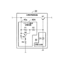
図1はこの発明に係る車載電子装置の電源制御回路の一実施の形態を示す回路図である。図1において、符号1は車載のバッテリであり、バッテリ1の正極側電源B+は電源制御回路10の正極側電源端子10aに供給され、バッテリ1の負極側電源B−は電源制御回路10の負極側電源入力端子10bに供給される。負極側電源入力端子10bは、電源制御回路10のグランドに接続されている。すなわち、バッテリ1の負極側電源B−は接地されている。
【0021】
符号2はイグニッションスイッチ(IGNSW)であり、このイグニッションスイッチ2がオン(導通)状態にされると、バッテリ1の正極側電源B+が電源制御回路10のイグニッション電源入力端子10cに供給される。
【0022】
符号100は第1の電子装置であり、この第1の電子装置100は電源制御回路10の第1の電源出力端子10dから定電圧電源VCの供給を受けて動作する。符号200は第2の電子装置であり、この第2の電子装置200は電源制御回路10の第2の電源出力端子10eから定電圧電源VDの供給を受けて動作する。
【0023】
符号10fは、イグニッションスイッチ2がオン(導通)状態にあることを示すイグニッションスイッチ検出信号ISの出力端子である。イグニッションスイッチオン検出信号ISは、第1の電子装置100のイグニッションスイッチオン検出信号入力端子IGKへ供給される。符号10gは、第1の電子装置100の電源供給保持信号出力端子DKHから出力される電源供給保持信号HSの入力端子である。なお、VCCは第1の電子装置100の正極側電源端子、GNDは第1の電子装置100の負極側電源端子(グランド端子)である。
【0024】
ここで、第1の電子装置100は、イグニッションスイッチ2がオフにされた状態では、基本的に電源の供給を受ける必要がない電子装置である。このような電子装置の例として、車両用メータ装置を挙げることができる。また、第2の電子装置200は、イグニッションスイッチ2の状態に拘らず常時給電を受ける必要がある電子装置で、このような電子装置の例として、時計装置や盗難防止装置等を挙げることができる。
【0025】
電源制御回路10は、バッテリ1から電力の供給を受けて、例えば出力電圧が5ボルトの定電圧電源VDを生成し、生成した定電圧電源VDを第2の電子装置200へ供給することができるとともに、電源スイッチ回路50を介して第1の電子装置100への電源供給/遮断を制御できるようにしたものである。
【0026】
この電源制御回路10は、エミッタフォロワ型の定電圧電源回路20と、第1の電子装置100に対する電源供給を制御する電源スイッチ回路50と、バイアス電流切替回路40のバイアス電流の切り替え及び電源スイッチ回路50のオン/オフ(給電/遮断)動作を切り替える切替制御回路60と、イグニッションスイッチ2の操作状態を検出して、イグニッションスイッチオン検出信号ISを第1の電子装置100へ供給するインタフェース回路70とからなる。
【0027】
定電圧電源回路20は、NPN型のトランジスタQ1と、この定電圧電源回路20の出力電圧を規定するための定電圧回路30と、この定電圧電源回路20内のバイアス電流を少なくとも2段階に切り替えるバイアス電流切替回路40とを備える。より具体的には、この定電圧電源回路20は、NPN型のトランジスタQ1と、定電圧回路30を構成する定電圧ダイオードD1と、バイアス電流切替回路40を構成する各抵抗R1〜R4及びPNP型のスイッチングトランジスタQ2とからなる。定電圧ダイオードD1は、そのカソードがNPN型のトランジスタQ1のベースに接続され、そのアノードがグランドに接続されている。
【0028】
NPN型のトランジスタQ1のエミッタとベースとの間に、第1のバイアス電流供給用抵抗R1が接続されている。PNP型のスイッチングトランジスタQ2と第2のバイアス電流供給用抵抗R2との直列接続回路が、第1のバイアス電流供給用抵抗R1に並列に接続されている。PNP型のスイッチングトランジスタQ2のエミッタとベースとの間に、エミッタ−ベース間抵抗R3が接続されている。PNP型のスイッチングトランジスタQ2のベースは、ベース抵抗R4を介して切替制御回路60の出力端子60aに接続されている。
【0029】
第1のバイアス電流供給用抵抗R1の抵抗値は大きな値(例えば、数100キロオーム程度)に設定されており、第2のバイアス電流供給用抵抗R2の抵抗値は第1のバイアス電流供給用抵抗R1よりも十分に小さい値(例えば数キロオーム〜10数キロオーム程度)に設定されている。したがって、PNP型のスイッチングトランジスタQ2がオフ状態(非導通状態)であるときには、第1のバイアス電流供給用抵抗R1を介して小さなバイアス電流が供給される。また、PNP型のスイッチングトランジスタQ2がオン状態(導通状態)に制御されると、第1のバイアス電流供給用抵抗R1を介して供給されるバイアス電流に第2のバイアス電流供給用抵抗R2を介して供給されるバイアス電流が加算されるので、大きな出力電流を供給するのに十分な比較的大きなバイアス電流がNPN型トランジスタQ1のベース及び定電圧回路30を構成する定電圧ダイオードD1に供給される。
【0030】
バッテリ1の正極側電源B+は、正極側電源入力端子10aからバッテリ逆接続保護用ダイオードD2と突入電流制限用抵抗R5との直列接続回路を介して、NPN型のトランジスタQ1のコレクタ及びバイアス電流切替回路40の入力端40aに供給される。
【0031】
なお、定電圧電源回路20の入力側(NPN型のトランジスタQ1のコレクタ側)とグランドとの間に、バッテリ電源に重畳されたサージ電圧を吸収するためのサージ電圧吸収用素子(例えば定電圧ダイオード)D3と電源平滑用コンデンサ(例えば電解コンデンサ)C1とがそれぞれ接続されている。
【0032】
定電圧電源回路20の出力側(NPN型のトランジスタQ1のエミッタ側)とグランドとの間に、定電圧電源VDの出力電圧を安定化するための電源平滑用コンデンサ(例えば電解コンデンサ)C2が接続されている。定電圧電源回路20から出力された定電圧電源VCは、第2の電源出力端子10eへ直接供給されるとともに、電源スイッチ回路50を介して第1の電源出力端子10dに供給される。
【0033】
電源スイッチ回路50は、PNP型のスイッチングトランジスタQ3と、エミッタ−ベース間抵抗R6と、ベース抵抗R7と、逆流防止用ダイオードD4とから構成されている。PNP型のスイッチングトランジスタQ3のエミッタは、定電圧電源回路20の出力側(NPN型のトランジスタQ1のエミッタ側)に接続され、PNP型のスイッチングトランジスタQ3のコレクタは、第1の電源出力端子10dに接続されている。PNP型のスイッチングトランジスタQ3のベースは、ベース抵抗R7及び逆流防止用ダイオードD4を介して切替制御回路60の出力端子60aに接続されている。
【0034】
電源スイッチ回路50の出力側(第1の電源出力端子10d)とグランドとの間には、定電圧電源VDの出力電圧を安定化するための電源平滑用コンデンサ(例えば電解コンデンサ)C3と、高周波雑音を吸収するためのノイズ吸収用コンデンサ(例えばセラミックコンデンサ)C4とがそれぞれ接続されている。
【0035】
切替制御回路60は、イグニッションスイッチ2がオン状態にされたときにオン(導通)状態となるNPN型のスイッチングトランジスタQ4と、そのトランジスタQ4のベース抵抗R8及びベース−エミッタ間抵抗R9と、電源供給保持信号HSが供給されたときにオン(導通状態)となるNPN型のスイッチングトランジスタQ5と、そのトランジスタQ5のベース抵抗R10及びベース−エミッタ間抵抗R11とからなる。各スイッチングトランジスタQ4,Q5のエミッタはそれぞれグランドに接続されている。各スイッチングトランジスタQ4,Q5のコレクタは、切替制御回路60の出力端子60aにそれぞれ接続されている。
【0036】
インタフェース回路70は、エミッタがグランドに接続されたNPN型のスイッチングトランジスタQ6と、ベース抵抗R12及びベース−エミッタ間抵抗R13とからなる。スイッチングトランジスタQ6のコレクタは、イグニッションスイッチオン検出信号出力端子10fに接続されている。
【0037】
イグニッションスイッチ2がオン(導通)状態にされると、バッテリ逆接続保護用ダイオードD5を介して切替制御回路60の入力端子60b及びインタフェース回路70の入力端子70aにイグニッション電源VIGN(バッテリ電源B+)が供給される。
【0038】
符号D6は、イグニッション電源VIGN側から定電圧電源回路20にイグニッション電源VIGN(バッテリ電源B+)を供給するためのダイオードであり、このダイオードD6のアノードはダイオードD5のカソード側に接続され、このダイオードD6のカソードはダイオードD2のカソード側に接続されている。なお、ダイオードD6のアノードをイグニッション電源入力端子10fに接続するようにしてもよい。
【0039】
図1に示す電源制御回路10は、イグニッションスイッチ2がオン状態にされると、切替制御回路60内のNPN型スイッチングトランジスタQ4がオン(導通)状態となる。これにより、電源スイッチ回路50内のPNP型スイッチングトランジスタQ3にベース電流が供給され、このトランジスタQ3がオン(導通)状態となって、第1の電子装置100へ定電圧電源VCを供給する。また、切替制御回路60内のNPN型スイッチングトランジスタQ4がオン(導通)状態となると、バイアス電流切替回路40内のPNP型スイッチングトランジスタQ2にベース電流が供給され、このトランジスタQ2がオン(導通)状態となるので、定電圧出力用のNPN型トランジスタQ1のベース電流が増加する。したがって、NPN型トランジスタQ1を介して負荷である各電子装置100,200へ供給可能な電流が増大される。
【0040】
また、イグニッションスイッチ2がオン状態にされると、インタフェース回路70内のNPN型スイッチングトランジスタQ6がオン(導通)状態となり、Lレベルのイグニッションスイッチオン検出信号ISが第1の電子装置100のイグニッションオン検出信号入力端子IGKに供給される。なお、本実施の形態では、イグニッションオン検出信号入力端子IGK側にプルアップ抵抗(図示しない)が設けられている。第1の電子装置100は、イグニッションスイッチオン検出信号ISに基づいてイグニッションスイッチ2がオン状態にあることを認識すると、Hレベルの電源供給保持信号HSを出力する。第1の電子装置100は、イグニッションスイッチ2がオフ(非導通)にされたことを認識すると、所定の処理が終了した時点で電源供給保持信号HSの出力を停止する。
【0041】
イグニッションスイッチ2がオフ(非導通)状態にされ、これに伴って切替制御回路60内の一方のNPN型スイッチングトランジスタQ4がオフ(非導通)となっても、他方のNPN型スイッチングトランジスタQ5は、第1の電子装置100から電源供給保持信号HSが供給されている期間は、オン(導通)状態となるので、電源スイッチ回路50の電源供給/遮断用のPNP型スイッチングトランジスタQ3はオン(導通)状態が継続され、第1の電子装置100に対する電源供給は継続される。また、バイアス電流切替回路40は、PNP型スイッチングトランジスタQ2のオン状態が継続されるので、定電圧電源回路20の負荷である第1の電子装置100に対して十分な電流を供給できる状態が継続される。
【0042】
そして、第1の電子装置100が所定の処理を終了した後に、電源供給保持信号HSの出力を停止すると、切替制御回路60内の他方のNPN型スイッチングトランジスタQ5がオフ(非導通)状態となり、電源スイッチ回路50内の電源供給/遮断用のPNP型スイッチングトランジスタQ3がオフ(非導通)状態となって、第1の電子装置100への定電圧電源VCの供給を遮断する。これと同時に、バイアス電流切替回路40内のPNP型スイッチングトランジスタQ2がオフ(非導通)状態となるので、定電圧出力用のNPN型トランジスタQ1のベース電流は、抵抗値の大きい第1のバイアス電流供給用抵抗R1によって規制されて小さな値に減少される。これにより、第1の電子装置100へ定電圧電源VCを供給していない状態における定電圧電源回路20内での消費電流が低減される。定電圧電源回路20内での消費電流が低減された状態であっても、例えば時計装置等の消費電流が小さいが常時電源供給を必要とする第2の電子装置200に対して定電圧電源VDを安定に供給することができるように、第1のバイアス電流供給用抵抗R1の抵抗値が設定されている。
【0043】
図2は定電圧回路の他の構成例を示す図である。定電圧電源回路20内の定電圧回路30は定電圧ダイオードD1を用いて構成する以外に、図2に示すようにトランジスタを用いた能動型の定電圧回路を用いて構成するようにしてもよい。
【0044】
ここで、図2(a)は、NPN型トランジスタQnとベース−エミッタ間抵抗Raとベース−コレクタ間抵抗Rbとからなる定電圧回路30Aを示しており、図2(b)はPNP型トランジスタQpとエミッタ−ベース間抵抗Rcとベース−コレクタ間抵抗Rdとからなる定電圧回路30Bを示している。図2(c)は、NPN型トランジスタQnのベースとエミッタ間に、ベース−エミッタ間抵抗RaとダイオードDaとの直列回路を接続することで、温度特性の改善を図った定電圧回路30Cを示しており、図2(d)は、PNP型トランジスタQpのエミッタとベース間にダイオードDbとエミッタ−ベース間抵抗Rcとの直列回路を接続することで、温度特性の改善を図った定電圧回路30Dを示している。
【0045】
図2(a)〜図2(d)に示したトランジスタを用いた能動型の定電圧回路30A〜30Dは、2つの抵抗の比によって定電圧回路30A〜30Dの電圧値が決定されるので、任意に電圧値を設定することができる。
【0046】
図3は第1の電子装置の一具体例として車両用メータ装置の構成を示すブロック図である。第1の電子装置100としての車両用メータ装置100Aは、CPU、ROM、RAM、入出力インタフェース回路、クロック発振回路、パワーオンリセット回路等を備えたCPU部110と、スピードメータ本体121を駆動するメータ駆動回路部120と、液晶表示装置131を用いて構成したオドメータ表示部131a及びトリップメータ表示部131bに該当する走行距離をそれぞれ表示させる表示装置駆動回路部130と、総走行距離のデータ及びユーザが任意にリセットできる走行距離のデータを格納する書き換え可能な不揮発性メモリ(例えばEEPROM)132とを備える。
【0047】
図4は車両用メータ装置の動作を示すフローチャートである。車両用メータ装置100Aは、電源端子VCCに定電圧電源VCが供給されると、先ずCPU部110の初期化処理がなされた後に(ステップS1)、ステップ2以降の動作が開始される。CPU部110は、イグニッションスイッチオン検出信号ISに基づいてイグニッションスイッチ2がオン状態であることを確認すると(ステップS2)、電源供給保持信号HSを出力し(ステップS3)、通常処理(メータ表示処理)を実行する(ステップS4)。
【0048】
ステップ4の通常処理(メータ表示処理)では、図3に示すようにCPU部110は、車速センサ140から供給されるパルス信号140aの周期を測定し、所定時間における複数の周期測定結果又は所定パルス数の周期測定結果の平均化処理を施して車速を求め、メータ駆動回路部120を介してスピードメータ本体121を駆動してメータの指針を回動させ、車速を指示させる。
【0049】
また、CPU部110は、車速センサ140から供給されるパルス信号をカウントし、所定のカウント数毎に所定の走行距離を積算して総走行距離及びユーザが任意にリセットできる走行距離を求め、表示装置駆動回路130を介して求めた各走行距離を表示装置駆動回路130のオドメータ表示部131a及びトリップメータ表示部131bにそれぞれ表示させる。この通常処理(メータ表示処理)は、イグニッションスイッチ2がオン状態である限り繰り返し継続される。
【0050】
図4に示すように、CPU部110は、イグニッションスイッチオン検出信号ISに基づいてイグニッションスイッチ2がオン状態からオフ状態になったことを検出すると(ステップS2)、ステップS5で終了処理を行なった後に、ステップS6で電源供給保持信号HSの出力を停止させる。これにより、車両用メータ装置100Aに対する定電圧電源VCの供給が遮断される。
【0051】
すなわち、イグニッションスイッチ2がオフ状態にされると、ステップS5でCPU部110は、スピードメータ本体121の指針をゼロ位置に戻すためのメータの帰零動作を行なうとともに、オドメータの積算値及びトリップメータの積算値を不揮発性メモリ(EEPROM)132にそれぞれ書き込んだ後に、ステップS6で電源供給保持信号HSの出力を停止させて、車両用メータ装置100Aに対する定電圧電源VCの供給が遮断させる。
【0052】
前述したように、図1に示した電源制御回路10は、第1の電子装置100である車両用メータ装置100Aからの電源供給保持信号HSの供給が停止されると、電源スイッチ回路50をオフ状態(非導通状態)にし、第1の電子装置100(車両用メータ装置100A)への定電圧電源VCの供給を停止する。さらに、電源制御回路10は、定電圧電源回路20のバイアス電流切替回路40内のPNP型スイッチングトランジスタQ2をオフ状態(非導通状態)にし、バイアス電流が小さい状態に切り替える。これにより、定電圧電源回路20内で不必要なバイアス電流が供給されるのを防止する。したがって、イグニッションスイッチ2がオフ状態でのいわゆる暗電流を低減するとともに、例えば時計装置等の常時給電を必要とする第2の電子装置200に対して定電圧電源VDを供給することができる。
【0053】
図5はバイアス電流切替回路の他の構成を示す回路部である。図5に示すバイアス電流切替回路40Aは、抵抗値が大きく(例えば、数100キロオーム程度)、その抵抗値に基づいて電源スイッチ回路50が非導通状態の時のバイアス電流を主として設定する第1のバイアス電流供給用抵抗R1と、第1のバイアス電流供給用抵抗R1よりも十分に小さい抵抗値(例えば数キロオーム〜10数キロオーム程度)で主として電源スイッチ回路50が導通状態の時のバイアス電流を設定する第2のバイアス電流供給用抵抗R2とを直列に接続し、PNP型のスイッチングトランジスタQ2を第1のバイアス電流供給用抵抗R1に並列に接続している。
【0054】
そして、図1に示した切替制御回路60内の各NPN型スイッチングトランジスタQ4,Q5のいずれかがオン状態となったときに、ベース抵抗R4を介してPNP型のスイッチングトランジスタQ2にベース電流が供給されて、PNP型のスイッチングトランジスタQ2のエミッタ−コレクタ間が導通状態になって、第1のバイアス電流供給用抵抗R1を短絡するようにしたものである。これにより、イグニッションスイッチ2がオン状態のとき、及び、電源供給保持信号HSが供給されている間は、定電圧出力用のNPN型トランジスタQ1のベースに大きな電流を供給することができるので、第1の電子装置100側に十分な電流を供給することができる。また、イグニッションスイッチ2がオフ状態であって、且つ、電源供給保持信号HSの出力が停止された状態では、PNP型のスイッチングトランジスタQ2がオフ状態になり、抵抗値が大きい第1のバイアス電流供給用抵抗R1と第2のバイアス電流供給用抵抗R2との直列接続回路によってバイアス電流を小さく抑える。これにより、第1の電子装置100への給電を遮断している状態で、定電圧電源回路20内部での消費電流を低減することができ、いわゆる暗電流を低減することができる。
【0055】
なお、本実施の形態では、バイアス電流切替回路40,40Aはバイアス電流を2段階に切り替える構成を示したが、電源スイッチ回路50を複数系統設け、複数の電子装置毎に、又は複数の電子装置グループ別に定電圧電源の供給/遮断を制御できる構成をとる場合には、定電圧電源を供給している電子装置の個数または電子装置グループのグループ数に応じて、定電圧電源回路20内のバイアス電流の値を多段階に切り替えるようにしてもよい。これにより、定電圧電源回路20内で不要に消費される電流を木目細かく低減することができる。
【0056】
【発明の効果】
以上説明したようにこの発明に係る車載電子装置の電源制御回路は、イグニッションスイッチがオン状態であるとき及び電子装置から電源供給保持信号が供給されているときは、バイアス電流切替回路をバイアス電流が大の状態に切り替えるとともに電源スイッチ回路を導通状態に制御するので、電源スイッチ回路を介して電子装置にその動作に必要な十分な電流(例えば数ミリアンペア〜数100ミリアンペア)を供給することができる。
【0057】
そして、この車載電子装置の電源制御回路は、イグニッションスイッチがオフ状態であって且つ電子装置から電源供給保持信号が供給されていないときは、バイアス電流切替回路をバイアス電流が小の状態に切り替えるとともに電源スイッチ回路を非導通状態に制御するので、電源スイッチ回路を介して給電を受ける電子装置への電源供給が完全に遮断されるとともに、定電圧電源回路内のバイアス電流を低減するので、イグニッションスイッチがオフにされた状態でのバッテリの消費電流(いわゆる暗電流)を低減することができる。
【図面の簡単な説明】
【図1】この発明に係る車載電子装置の電源制御回路の一実施の形態を示す回路図である。
【図2】この発明に係る車載電子装置の電源制御回路の定電圧回路の他の構成例を示す図である。
【図3】第1の電子装置の一具体例として車両用メータ装置の構成を示すブロック図である。
【図4】図3に示した車両用メータ装置の動作を示すフローチャートである。
【図5】この発明に係る車載電子装置の電源制御回路のバイアス電流切替回路の他の構成を示す回路部である。
【符号の説明】
1 バッテリ
2 イグニッションスイッチ
10 電源制御回路
20 定電圧電源回路
30 定電圧回路
40、40A バイアス電流切替回路
50 電源スイッチ回路
60 切替制御回路
70 インタフェース回路
100 第1の電子装置
200 第2の電子装置
D1 定電圧回路を構成する定電圧ダイオード
HS 電源供給保持信号
IS イグニッションスイッチオン検出信号
Q1 定電圧電源回路を構成するNPN型トランジスタ
Q2 バイアス電流切替回路を構成するPNP型スイッチングトランジスタ
Q3 電源スイッチ回路を構成するPNP型スイッチングトランジスタ
Q4 切替制御回路を構成するNPN型スイッチングトランジスタ
Q5 切替制御回路を構成するNPN型スイッチングトランジスタ
Q6 インタフェース回路を構成するNPN型スイッチングトランジスタ
R1 バイアス電流切替回路を構成する第1のバイアス電流供給用抵抗
R2 バイアス電流切替回路を構成する第2のバイアス電流供給用抵抗
VC 定電圧電源(電源スイッチ回路の前段)
VD 定電圧電源(電源スイッチ回路の後段)[0001]
TECHNICAL FIELD OF THE INVENTION
The present invention relates to a power supply control device for an in-vehicle electronic device, and more particularly, to a power supply control device that switches the bias current of an emitter follower type constant voltage power supply circuit to reduce power consumed by the constant voltage power supply circuit during standby. The present invention relates to a power supply control circuit of an electronic device.
[0002]
[Prior art]
A power switch circuit is provided before the constant voltage circuit (voltage converter) that supplies constant voltage power to the ECU (microcomputer). When the ECU (microcomputer) stops operating, the power switch circuit is turned off (no power supply) It is conventionally known that the power supply to an ECU (microcomputer) is cut off to thereby reduce the dark current and thereby save power (see Patent Documents 1 and 4).
[0003]
The output voltage of the constant voltage circuit is directly supplied to the CPU, and a switch circuit for controlling power supply is provided between the output side of the constant voltage circuit and a peripheral circuit of the CPU, and the ignition switch of the CPU is turned off. After performing a predetermined process with the switch circuit held in a conductive state, the switch circuit is controlled to an off (non-conductive) state to cut off the power supply to the peripheral circuits of the CPU, thereby reducing the consumption during standby. A display device for a vehicle in which the current is reduced is conventionally known (see Patent Document 2).
A battery positive power supply (B +) is supplied to the collector of the NPN transistor, and a constant voltage (Zener) diode is connected between the base and the battery negative power supply (B−) or ground (ground potential). And an emitter follower-type constant voltage circuit that outputs a constant voltage set based on the breakdown voltage (Zener voltage) of a constant voltage (Zener) diode from the emitter side. Is conventionally known (see, for example, Patent Documents 3 and 5). The output voltage VCC of the emitter follower-type constant voltage circuit is VCC = VZD-VBE, where the breakdown voltage (Zener voltage) of the constant voltage diode is VZD and the base-emitter voltage of the NPN transistor is VBE. Become.
[0004]
A series circuit of a switch circuit and a bias resistor is connected between the collector and the base of an NPN transistor that forms an emitter follower-type constant voltage circuit. When the CPU detects that the ignition switch has been turned off, a predetermined process is performed. After performing, for example, a zero return operation of the meter pointer, the switch circuit is turned off to stop the output of the constant voltage circuit and cut off the power supply to the CPU, thereby eliminating unnecessary power consumption of the CPU. Such a driving device for a vehicle instrument is conventionally known (see Patent Document 4).
[0005]
A first bias resistor is connected between a collector and a base of an NPN transistor constituting an emitter follower-type constant voltage circuit, and a series circuit of a switch circuit and a second bias resistor is connected in parallel with the first bias resistor. When the motor is driven (when the load current is large), the switch circuit is turned on (conducting state) to substantially reduce the resistance value of the bias resistor, thereby reducing the output of the constant voltage circuit. By increasing the current and turning off the switch circuit (non-conducting state) when the motor is not driven (when the load current is small), the resistance value of the bias resistor is substantially increased, and the bias current is increased. 2. Description of the Related Art A time constant voltage circuit for a watch in which the power supply battery is reduced by reducing the power consumption has been conventionally known (see Patent Document 5).
[0006]
[Patent Document 1]
JP-A-2002-304240
[Patent Document 2]
JP-A-11-255047
[Patent Document 3]
JP-A-11-85293 (FIG. 16)
[Patent Document 4]
JP-A-2002-90185
[Patent Document 5]
Japanese Utility Model Laid-Open No. 5-59386 (Claims for utility model registration and FIG. 1)
[0007]
[Problems to be solved by the invention]
2. Description of the Related Art In recent years, various electronic devices are mounted on vehicles (including motorcycles and the like). Many of these electronic devices include a CPU (microcomputer). When the ignition switch is turned off, the electronic device mounted on the vehicle includes (1) a device that does not need to operate (that is, a device that can cut off power supply) and (2) a device that performs a predetermined process. After that, there are those that stop the operation after that (that is, the power supply may be cut off after a predetermined time) and those that need to continue the operation (3) (that is, those that need the power supply). A device that needs to continue operation includes a clock device, a timer unit in the clock device, a device that monitors theft of a vehicle, and the like.
[0008]
When supplying power to both electronic devices that can be powered off from a single constant-voltage power supply circuit and electronic devices that require constant power supply, a power switch circuit should be provided before the constant-voltage power supply circuit. Can not.
[0009]
Therefore, when a constant voltage power supply is supplied from a single constant voltage power supply circuit to a plurality of electronic devices, (1) For an electronic device that can shut off power supply when the ignition switch is off, A switch circuit is provided between the output side of the constant voltage power supply circuit and the electronic device, and the power supply to the electronic device can be stopped by controlling the switch circuit to be in a non-conductive state immediately when the ignition switch is turned off. (2) For an electronic device whose power supply may be cut off after a predetermined time has elapsed from the time when the ignition switch is turned off, a switch circuit is provided between the output side of the constant voltage power supply circuit and the electronic device; By maintaining the conduction state of the switch circuit for a predetermined time by the output of the electronic device side, the electronic device is connected to the electronic device after a predetermined time has elapsed since the ignition switch was turned off. Supplying a can be stopped, (3) by supplying the output of the constant voltage power supply circuit directly to electronic devices requiring backup power supply of clock device or the like, can be always supplied power. Thus, unnecessary power consumption can be eliminated by cutting off the power supply for each electronic device.
[0010]
However, the positive-side battery power (B +) is supplied to the collector of the NPN transistor, and a constant voltage (Zener) diode is connected between the base and the ground (ground potential, negative-side battery power (B-)). An emitter-follower type constant voltage power supply circuit is configured so that a bias resistor is connected between the power supply and the base, and a constant voltage set based on the breakdown voltage (Zener) of the constant voltage diode is output from the emitter side. If so, the following problems arise.
[0011]
Based on the maximum output current of the constant voltage power supply circuit (that is, the maximum value of the current when all the electronic devices powered by the constant voltage power supply circuit are operating with the ignition switch turned on). Since the value is set, in a state where power is supplied only to an electronic device that requires constant power supply such as a clock device, an unnecessary bias current flows to the constant voltage diode via the bias resistor, Useless power is consumed in the constant voltage power supply circuit.
[0012]
The present invention has been made to solve such a problem, and in a standby state in which the current supplied from a constant voltage power supply circuit to a load (electronic device) is small, the bias current of the constant voltage power supply circuit is reduced to reduce the constant current. It is an object of the present invention to provide a power supply control circuit for an in-vehicle electronic device in which unnecessary power consumption in a voltage power supply circuit is eliminated.
[0013]
[Means for Solving the Problems]
In order to solve the above-mentioned problems, a power supply control circuit for an in-vehicle electronic device according to the present invention includes a collector side of an NPN transistor as an input terminal of a positive power supply of a battery, an emitter side of the transistor as a constant voltage output terminal, A bias that connects a constant voltage circuit between the base and the negative electrode side (ground) of the battery, and switches the value of the bias current supplied to the base of the transistor and the constant voltage circuit between the collector and the base of the transistor in at least two stages. An emitter-follower-type constant-voltage power supply circuit connected to a current switching circuit, and a power supply to the electronic device is controlled by being interposed between the constant-voltage output terminal of the constant-voltage power supply circuit and the power supply terminal of the electronic device. Power supply switch circuit and the power supply holding signal is supplied when the ignition switch is on and from the electronic device When the bias switch is in the ON state, the bias current switching circuit is switched to the state in which the bias current is large, and the power switch circuit is controlled to the conductive state, and the ignition switch is in the OFF state and the power supply holding signal is supplied from the electronic device. A switching control circuit that switches the bias current switching circuit to a state where the bias current is small and controls the power switch circuit to a non-conductive state when there is no bias current switching circuit.
[0014]
The power supply control circuit of the vehicle-mounted electronic device according to the present invention switches the bias current switching circuit to a state where the bias current is large when the ignition switch is on and when the power supply holding signal is supplied from the electronic device. At the same time, the power supply switch circuit is controlled to a conductive state. Thus, a large current (for example, several milliamps to several hundred milliamps) can be supplied to the electronic device via the power switch circuit.
[0015]
When the ignition switch is in the off state and the power supply holding signal is not supplied from the electronic device, the power supply control circuit of the vehicle-mounted electronic device switches the bias current switching circuit to a state in which the bias current is small and The power switch circuit is controlled to be non-conductive. As a result, power supply to the electronic device that receives power supply via the power switch circuit is completely cut off.
[0016]
For a constant power supply type electronic device (for example, a clock device or a theft monitoring device) that needs to supply power even when the ignition switch is off, the constant voltage power supply circuit does not pass through the power supply switch circuit. Although the power is supplied directly from the constant voltage output terminal, the current consumption of the constantly powered electronic device is extremely smaller than the consumed current of the electronic device supplied with power via the power switch circuit.
[0017]
Therefore, the power consumption in the constant voltage power supply circuit is reduced by controlling the power supply switch circuit to a non-conductive state and switching the bias current switching circuit to a state in which the bias current is small. Thus, even when a voltage-stabilized power supply (constant-voltage power supply) is constantly supplied to, for example, a timepiece device via a constant-voltage power supply circuit, the power is supplied from the vehicle-mounted battery when the ignition switch is turned off. Current (so-called dark current) can be greatly reduced.
[0018]
Note that the constant voltage circuit is configured using a constant voltage diode (Zener diode) so that a single element can generate a constant voltage. Thereby, the configuration of the constant voltage power supply circuit can be simplified.
[0019]
BEST MODE FOR CARRYING OUT THE INVENTION
Hereinafter, preferred embodiments of the present invention will be described with reference to the accompanying drawings.
[0020]
FIG. 1 is a circuit diagram showing one embodiment of a power supply control circuit of a vehicle-mounted electronic device according to the present invention. In FIG. 1, reference numeral 1 denotes a vehicle-mounted battery, a positive power supply B + of the battery 1 is supplied to a positive power terminal 10 a of a power control circuit 10, and a negative power supply B− of the battery 1 is a negative power supply of the power control circuit 10. It is supplied to the side power input terminal 10b. The negative power input terminal 10b is connected to the ground of the power control circuit 10. That is, the negative power supply B- of the battery 1 is grounded.
[0021]
Reference numeral 2 denotes an ignition switch (IGNSW). When the ignition switch 2 is turned on (conducting), the positive power supply B + of the battery 1 is supplied to an ignition power input terminal 10 c of the power control circuit 10.
[0022]
Reference numeral 100 denotes a first electronic device. The first electronic device 100 operates by receiving a constant voltage power supply VC from a first power supply output terminal 10d of the power supply control circuit 10. Reference numeral 200 denotes a second electronic device. The second electronic device 200 operates by receiving a constant voltage power supply VD from a second power supply output terminal 10e of the power supply control circuit 10.
[0023]
Reference numeral 10f is an output terminal of an ignition switch detection signal IS indicating that the ignition switch 2 is in an ON (conductive) state. The ignition switch on detection signal IS is supplied to an ignition switch on detection signal input terminal IGK of the first electronic device 100. Reference numeral 10g denotes an input terminal of the power supply holding signal HS output from the power supply holding signal output terminal DKH of the first electronic device 100. Note that VCC is a positive power supply terminal of the first electronic device 100, and GND is a negative power supply terminal (ground terminal) of the first electronic device 100.
[0024]
Here, the first electronic device 100 is basically an electronic device that does not need to be supplied with power when the ignition switch 2 is turned off. An example of such an electronic device is a vehicle meter device. The second electronic device 200 is an electronic device that needs to be constantly supplied with power irrespective of the state of the ignition switch 2, and examples of such an electronic device include a clock device and an anti-theft device. .
[0025]
The power supply control circuit 10 receives the supply of power from the battery 1, generates a constant voltage power supply VD having an output voltage of, for example, 5 volts, and can supply the generated constant voltage power supply VD to the second electronic device 200. At the same time, power supply / interruption to the first electronic device 100 can be controlled via the power switch circuit 50.
[0026]
The power supply control circuit 10 includes an emitter follower-type constant voltage power supply circuit 20, a power supply switch circuit 50 for controlling power supply to the first electronic device 100, a bias current switching circuit 40 for switching a bias current and a power supply switch circuit. A switching control circuit 60 for switching on / off (supply / cut off) operations of the switch 50; an interface circuit 70 for detecting an operation state of the ignition switch 2 and supplying an ignition switch on detection signal IS to the first electronic device 100; Consists of
[0027]
The constant voltage power circuit 20 switches an NPN transistor Q1, a constant voltage circuit 30 for defining the output voltage of the constant voltage power circuit 20, and a bias current in the constant voltage power circuit 20 in at least two stages. And a bias current switching circuit 40. More specifically, the constant voltage power supply circuit 20 includes an NPN type transistor Q1, a constant voltage diode D1 forming a constant voltage circuit 30, a resistor R1 to R4 forming a bias current switching circuit 40, and a PNP type transistor. Switching transistor Q2. The constant voltage diode D1 has a cathode connected to the base of the NPN transistor Q1 and an anode connected to the ground.
[0028]
A first bias current supply resistor R1 is connected between the emitter and the base of the NPN transistor Q1. A series connection circuit of a PNP-type switching transistor Q2 and a second bias current supply resistor R2 is connected in parallel to the first bias current supply resistor R1. An emitter-base resistor R3 is connected between the emitter and the base of the PNP switching transistor Q2. The base of the PNP type switching transistor Q2 is connected to the output terminal 60a of the switching control circuit 60 via the base resistor R4.
[0029]
The resistance value of the first bias current supply resistor R1 is set to a large value (for example, about several hundred kilohms), and the resistance value of the second bias current supply resistor R2 is set to the first bias current supply resistor. The value is set to a value sufficiently smaller than R1 (for example, about several kilo-ohms to about several tens of kilo-ohms). Therefore, when the PNP-type switching transistor Q2 is off (non-conductive), a small bias current is supplied via the first bias current supply resistor R1. When the PNP-type switching transistor Q2 is turned on (conducting state), the bias current supplied via the first bias current supply resistor R1 is supplied via the second bias current supply resistor R2. The bias current supplied is added, so that a relatively large bias current sufficient to supply a large output current is supplied to the base of the NPN transistor Q1 and the constant voltage diode D1 constituting the constant voltage circuit 30. .
[0030]
The positive power supply B + of the battery 1 is switched from the positive power input terminal 10a to the collector and bias current of the NPN transistor Q1 via a series connection circuit of a battery reverse connection protection diode D2 and an inrush current limiting resistor R5. The signal is supplied to the input terminal 40a of the circuit 40.
[0031]
A surge voltage absorbing element (for example, a constant voltage diode) for absorbing a surge voltage superimposed on the battery power supply is provided between the input side of the constant voltage power supply circuit 20 (collector side of the NPN transistor Q1) and the ground. ) D3 and a power supply smoothing capacitor (for example, an electrolytic capacitor) C1 are connected to each other.
[0032]
A power supply smoothing capacitor (for example, an electrolytic capacitor) C2 for stabilizing the output voltage of the constant voltage power supply VD is connected between the output side of the constant voltage power supply circuit 20 (the emitter side of the NPN transistor Q1) and the ground. Have been. The constant voltage power supply VC output from the constant voltage power supply circuit 20 is directly supplied to the second power supply output terminal 10e and is also supplied to the first power supply output terminal 10d via the power supply switch circuit 50.
[0033]
The power switch circuit 50 includes a PNP-type switching transistor Q3, an emitter-base resistor R6, a base resistor R7, and a backflow prevention diode D4. The emitter of the PNP type switching transistor Q3 is connected to the output side of the constant voltage power supply circuit 20 (the emitter side of the NPN type transistor Q1), and the collector of the PNP type switching transistor Q3 is connected to the first power supply output terminal 10d. It is connected. The base of the PNP type switching transistor Q3 is connected to the output terminal 60a of the switching control circuit 60 via the base resistor R7 and the backflow prevention diode D4.
[0034]
A power supply smoothing capacitor (for example, an electrolytic capacitor) C3 for stabilizing the output voltage of the constant voltage power supply VD is provided between the output side (first power supply output terminal 10d) of the power supply switch circuit 50 and the ground. A noise absorbing capacitor (for example, a ceramic capacitor) C4 for absorbing noise is connected to each.
[0035]
The switching control circuit 60 includes an NPN-type switching transistor Q4 that is turned on (conducting) when the ignition switch 2 is turned on, a base resistor R8 and a base-emitter resistor R9 of the transistor Q4, and power supply. The transistor Q5 includes an NPN-type switching transistor Q5 that is turned on (conducting state) when the holding signal HS is supplied, and a base resistor R10 and a base-emitter resistor R11 of the transistor Q5. The emitters of the switching transistors Q4 and Q5 are respectively connected to the ground. The collectors of the switching transistors Q4 and Q5 are connected to the output terminal 60a of the switching control circuit 60, respectively.
[0036]
The interface circuit 70 includes an NPN-type switching transistor Q6 having an emitter connected to the ground, a base resistor R12, and a base-emitter resistor R13. The collector of the switching transistor Q6 is connected to the ignition switch on detection signal output terminal 10f.
[0037]
When the ignition switch 2 is turned on (conducting), the ignition power supply VIGN (battery power supply B +) is applied to the input terminal 60b of the switching control circuit 60 and the input terminal 70a of the interface circuit 70 via the battery reverse connection protection diode D5. Supplied.
[0038]
Reference numeral D6 denotes a diode for supplying an ignition power supply VIGN (battery power supply B +) from the ignition power supply VIGN side to the constant voltage power supply circuit 20, and the anode of the diode D6 is connected to the cathode side of the diode D5. Is connected to the cathode side of the diode D2. Note that the anode of the diode D6 may be connected to the ignition power input terminal 10f.
[0039]
In the power supply control circuit 10 shown in FIG. 1, when the ignition switch 2 is turned on, the NPN switching transistor Q4 in the switching control circuit 60 is turned on (conducting). As a result, the base current is supplied to the PNP switching transistor Q3 in the power switch circuit 50, and the transistor Q3 is turned on (conductive) to supply the constant voltage power supply VC to the first electronic device 100. When the NPN switching transistor Q4 in the switching control circuit 60 is turned on (conducting), a base current is supplied to the PNP switching transistor Q2 in the bias current switching circuit 40, and the transistor Q2 is turned on (conducting). Therefore, the base current of the NPN transistor Q1 for outputting a constant voltage increases. Therefore, the current that can be supplied to each of the electronic devices 100 and 200 as loads via the NPN transistor Q1 is increased.
[0040]
When the ignition switch 2 is turned on, the NPN switching transistor Q6 in the interface circuit 70 is turned on (conducting), and the L-level ignition switch on detection signal IS turns on the ignition of the first electronic device 100. It is supplied to the detection signal input terminal IGK. In this embodiment, a pull-up resistor (not shown) is provided on the side of the ignition-on detection signal input terminal IGK. When the first electronic device 100 recognizes that the ignition switch 2 is on based on the ignition switch on detection signal IS, it outputs an H level power supply holding signal HS. When recognizing that the ignition switch 2 has been turned off (disconnected), the first electronic device 100 stops outputting the power supply holding signal HS when predetermined processing is completed.
[0041]
When the ignition switch 2 is turned off (non-conducting) and accordingly one of the NPN switching transistors Q4 in the switching control circuit 60 is turned off (non-conducting), the other NPN-type switching transistor Q5 Since the power supply holding signal HS is being supplied from the first electronic device 100, the PNP switching transistor Q3 for power supply / interruption of the power switch circuit 50 is on (conductive) because the power supply holding signal HS is supplied. The state is continued, and the power supply to the first electronic device 100 is continued. Further, the bias current switching circuit 40 keeps the ON state of the PNP type switching transistor Q2, so that the state where a sufficient current can be supplied to the first electronic device 100 which is the load of the constant voltage power supply circuit 20 continues. Is done.
[0042]
Then, when the output of the power supply holding signal HS is stopped after the first electronic device 100 completes the predetermined processing, the other NPN type switching transistor Q5 in the switching control circuit 60 is turned off (non-conductive), The PNP type switching transistor Q3 for power supply / interruption in the power switch circuit 50 is turned off (non-conductive), and the supply of the constant voltage power VC to the first electronic device 100 is interrupted. At the same time, the PNP switching transistor Q2 in the bias current switching circuit 40 is turned off (non-conductive), so that the base current of the constant voltage output NPN transistor Q1 is the first bias current having a large resistance value. It is regulated by the supply resistor R1 and reduced to a small value. As a result, the current consumption in the constant voltage power supply circuit 20 when the constant voltage power supply VC is not supplied to the first electronic device 100 is reduced. Even when the current consumption in the constant voltage power supply circuit 20 is reduced, the constant voltage power supply VD is supplied to the second electronic device 200 that consumes a small amount of current but requires a constant power supply, such as a clock device. Is set so that the first bias current supply resistor R1 can be supplied stably.
[0043]
FIG. 2 is a diagram showing another configuration example of the constant voltage circuit. The constant voltage circuit 30 in the constant voltage power supply circuit 20 may be configured using an active constant voltage circuit using a transistor as shown in FIG. 2 in addition to the configuration using the constant voltage diode D1. .
[0044]
Here, FIG. 2A shows a constant voltage circuit 30A including an NPN transistor Qn, a base-emitter resistor Ra, and a base-collector resistor Rb, and FIG. 2B shows a PNP transistor Qp. And a constant-voltage circuit 30B including an emitter-base resistance Rc and a base-collector resistance Rd. FIG. 2C shows a constant voltage circuit 30C in which a series circuit of a base-emitter resistor Ra and a diode Da is connected between the base and the emitter of the NPN transistor Qn to improve the temperature characteristics. FIG. 2D shows a constant voltage circuit 30D having an improved temperature characteristic by connecting a series circuit of a diode Db and an emitter-base resistor Rc between the emitter and the base of the PNP transistor Qp. Is shown.
[0045]
In the active type constant voltage circuits 30A to 30D using the transistors shown in FIGS. 2A to 2D, the voltage values of the constant voltage circuits 30A to 30D are determined by the ratio of two resistors. The voltage value can be set arbitrarily.
[0046]
FIG. 3 is a block diagram showing a configuration of a vehicle meter device as a specific example of the first electronic device. The vehicle meter device 100A as the first electronic device 100 drives a CPU unit 110 including a CPU, a ROM, a RAM, an input / output interface circuit, a clock oscillation circuit, a power-on reset circuit, and the like, and a speedometer main body 121. A meter driving circuit unit 120, a display device driving circuit unit 130 for displaying the mileage corresponding to the odometer display unit 131a and the trip meter display unit 131b configured using the liquid crystal display device 131, and data of the total mileage and the user Has a rewritable nonvolatile memory (for example, an EEPROM) 132 for storing data of the traveling distance which can be arbitrarily reset.
[0047]
FIG. 4 is a flowchart showing the operation of the vehicle meter device. When the constant voltage power supply VC is supplied to the power supply terminal VCC, the vehicle meter device 100A first performs an initialization process of the CPU unit 110 (step S1), and then starts the operation of step 2 and thereafter. When the CPU unit 110 confirms that the ignition switch 2 is on based on the ignition switch on detection signal IS (step S2), it outputs a power supply holding signal HS (step S3), and performs normal processing (meter display processing). ) (Step S4).
[0048]
In the normal processing (meter display processing) in step 4, as shown in FIG. 3, the CPU section 110 measures the cycle of the pulse signal 140a supplied from the vehicle speed sensor 140 and obtains a plurality of cycle measurement results for a predetermined time or a predetermined pulse. The vehicle speed is obtained by averaging the number of period measurement results, and the speedometer main body 121 is driven via the meter driving circuit unit 120 to rotate the pointer of the meter to indicate the vehicle speed.
[0049]
Further, the CPU unit 110 counts the pulse signal supplied from the vehicle speed sensor 140, integrates a predetermined traveling distance for each predetermined count, obtains a total traveling distance and a traveling distance that can be reset arbitrarily by the user, and displays the total traveling distance. Each travel distance obtained via the device drive circuit 130 is displayed on the odometer display section 131a and the trip meter display section 131b of the display device drive circuit 130, respectively. This normal processing (meter display processing) is repeated repeatedly as long as the ignition switch 2 is on.
[0050]
As shown in FIG. 4, when the CPU unit 110 detects that the ignition switch 2 has changed from the on state to the off state based on the ignition switch on detection signal IS (step S2), the CPU unit 110 performs termination processing in step S5. Later, in step S6, the output of the power supply holding signal HS is stopped. As a result, the supply of the constant voltage power supply VC to the vehicle meter device 100A is cut off.
[0051]
That is, when the ignition switch 2 is turned off, in step S5, the CPU unit 110 performs a zero return operation of the meter for returning the pointer of the speedometer main body 121 to the zero position, and simultaneously performs the integration of the odometer and the trip meter. Is written in the nonvolatile memory (EEPROM) 132, the output of the power supply holding signal HS is stopped in step S6, and the supply of the constant voltage power supply VC to the vehicle meter device 100A is cut off.
[0052]
As described above, the power supply control circuit 10 shown in FIG. 1 turns off the power supply switch circuit 50 when the supply of the power supply holding signal HS from the vehicle meter device 100A as the first electronic device 100 is stopped. State (non-conduction state), and the supply of the constant voltage power supply VC to the first electronic device 100 (vehicle meter device 100A) is stopped. Further, the power supply control circuit 10 turns off the PNP-type switching transistor Q2 in the bias current switching circuit 40 of the constant voltage power supply circuit 20 (non-conducting state), and switches the bias current to a small state. This prevents unnecessary bias current from being supplied in the constant voltage power supply circuit 20. Therefore, while reducing the so-called dark current when the ignition switch 2 is in the off state, the constant voltage power supply VD can be supplied to the second electronic device 200 that requires constant power supply, such as a clock device.
[0053]
FIG. 5 is a circuit diagram showing another configuration of the bias current switching circuit. The bias current switching circuit 40A shown in FIG. 5 has a large resistance value (for example, about several hundreds of kohms), and mainly sets a bias current when the power switch circuit 50 is in a non-conductive state based on the resistance value. The bias current is mainly set when the power supply switch circuit 50 is in the conductive state with the bias current supply resistor R1 and a resistance value sufficiently smaller than the first bias current supply resistor R1 (for example, about several kilohms to about several tens of kiloohms). The second bias current supply resistor R2 is connected in series, and a PNP-type switching transistor Q2 is connected in parallel to the first bias current supply resistor R1.
[0054]
When one of the NPN switching transistors Q4 and Q5 in the switching control circuit 60 shown in FIG. 1 is turned on, a base current is supplied to the PNP switching transistor Q2 via the base resistor R4. Then, the emitter-collector of the PNP-type switching transistor Q2 is brought into a conductive state, and the first bias current supply resistor R1 is short-circuited. Accordingly, a large current can be supplied to the base of the NPN transistor Q1 for outputting a constant voltage when the ignition switch 2 is turned on and while the power supply holding signal HS is being supplied. A sufficient current can be supplied to the one electronic device 100 side. Further, when the ignition switch 2 is off and the output of the power supply holding signal HS is stopped, the PNP-type switching transistor Q2 is turned off, and the first bias current supply having a large resistance value is performed. The bias current is suppressed to be small by a series connection circuit of the first resistor R1 and the second bias current supply resistor R2. Accordingly, in a state where power supply to the first electronic device 100 is cut off, current consumption inside the constant voltage power supply circuit 20 can be reduced, and so-called dark current can be reduced.
[0055]
In the present embodiment, the configuration in which the bias current switching circuits 40 and 40A switch the bias current in two stages has been described. However, a plurality of power supply switch circuits 50 are provided, and for each of a plurality of electronic devices or a plurality of electronic devices. In the case where the supply / cutoff of the constant voltage power supply can be controlled for each group, the bias in the constant voltage power supply circuit 20 can be controlled according to the number of electronic devices supplying the constant voltage power supply or the number of electronic device groups. The current value may be switched in multiple stages. This makes it possible to finely reduce unnecessary current consumed in the constant voltage power supply circuit 20.
[0056]
【The invention's effect】
As described above, the power supply control circuit of the in-vehicle electronic device according to the present invention provides the bias current switching circuit with the bias current when the ignition switch is on and when the power supply holding signal is supplied from the electronic device. Since the state is switched to the large state and the power switch circuit is controlled to the conductive state, a sufficient current (for example, several milliamps to several hundred milliamps) necessary for the operation can be supplied to the electronic device via the power switch circuit.
[0057]
When the ignition switch is off and the power supply holding signal is not supplied from the electronic device, the power supply control circuit of the on-vehicle electronic device switches the bias current switching circuit to a state in which the bias current is small and Since the power switch circuit is controlled to be in a non-conductive state, the power supply to the electronic device to which power is supplied via the power switch circuit is completely cut off, and the bias current in the constant voltage power circuit is reduced, so that the ignition switch is turned on. , The consumption current of the battery (so-called dark current) can be reduced.
[Brief description of the drawings]
FIG. 1 is a circuit diagram showing an embodiment of a power supply control circuit of a vehicle-mounted electronic device according to the present invention.
FIG. 2 is a diagram showing another configuration example of the constant voltage circuit of the power supply control circuit of the vehicle-mounted electronic device according to the present invention.
FIG. 3 is a block diagram illustrating a configuration of a vehicle meter device as a specific example of a first electronic device.
FIG. 4 is a flowchart showing an operation of the vehicle meter device shown in FIG. 3;
FIG. 5 is a circuit diagram showing another configuration of the bias current switching circuit of the power supply control circuit of the vehicle-mounted electronic device according to the present invention.
[Explanation of symbols]
1 Battery
2 Ignition switch
10. Power supply control circuit
20 constant voltage power supply circuit
30 constant voltage circuit
40, 40A bias current switching circuit
50 Power switch circuit
60 Switching control circuit
70 Interface Circuit
100 First electronic device
200 Second electronic device
D1 Constant voltage diode that composes constant voltage circuit
HS power supply hold signal
IS ignition switch on detection signal
Q1 NPN transistor that forms a constant voltage power supply circuit
Q2 PNP switching transistor forming bias current switching circuit
Q3 PNP type switching transistor that constitutes power switch circuit
Q4 NPN-type switching transistor constituting a switching control circuit
Q5 NPN-type switching transistor constituting a switching control circuit
Q6 NPN-type switching transistor constituting interface circuit
R1 A first bias current supply resistor constituting a bias current switching circuit
R2 A second bias current supply resistor constituting a bias current switching circuit
VC constant voltage power supply (before power switch circuit)
VD constant voltage power supply (after power switch circuit)