JP2004343733A - Temperature compensated oscillator - Google Patents
Temperature compensated oscillator Download PDFInfo
- Publication number
- JP2004343733A JP2004343733A JP2004126019A JP2004126019A JP2004343733A JP 2004343733 A JP2004343733 A JP 2004343733A JP 2004126019 A JP2004126019 A JP 2004126019A JP 2004126019 A JP2004126019 A JP 2004126019A JP 2004343733 A JP2004343733 A JP 2004343733A
- Authority
- JP
- Japan
- Prior art keywords
- capacitance element
- circuit
- mos
- voltage signal
- terminal
- Prior art date
- Legal status (The legal status is an assumption and is not a legal conclusion. Google has not performed a legal analysis and makes no representation as to the accuracy of the status listed.)
- Granted
Links
Images


Landscapes
- Oscillators With Electromechanical Resonators (AREA)
Abstract
Description
本発明は水晶等の圧電素子を使用した発振器に関し、特に簡単な回路構成によって周波数の温度補償が可能で、IC化に適した温度補償発振器に関する。 The present invention relates to an oscillator using a piezoelectric element such as a crystal, and more particularly to a temperature-compensated oscillator suitable for ICs, which can perform frequency temperature compensation with a simple circuit configuration.
近年、圧電素子、例えば水晶振動子を使用した発振器では周波数安定度は勿論のこと、小型化、低価格化等の要求が厳しく、更には、通信方式のデジタル化が進むにつれて、従来問題とならなかった雑音比特性(C/N特性)の向上が望まれている。発振器の出力周波数は種々の要因で変化するが、比較的周波数の安定度が高い水晶発振器においても、周囲温度、電源電圧及び出力負荷等の条件変化による周波数変動があり、これ等に対応する手段は種々のものが講じられている。例えば温度変化に関しては水晶発振器に温度補償回路を付加し、この温度補償水晶発振器(以下、TCXOと称す)の発振ループ中の負荷容量を変化させて、水晶振動子固有の温度−周波数特性を相殺するように前記負荷容量を温度変化に対して制御するものがある。 In recent years, in oscillators using piezoelectric elements, for example, crystal oscillators, not only frequency stability, but also demands for downsizing and price reduction are strict. It has been desired to improve the noise ratio characteristics (C / N characteristics) that did not exist. Although the output frequency of the oscillator changes due to various factors, even in a crystal oscillator having a relatively high frequency stability, there are frequency fluctuations due to changes in conditions such as ambient temperature, power supply voltage and output load. Various things are taken. For example, with respect to a temperature change, a temperature compensation circuit is added to the crystal oscillator, and the load capacitance in the oscillation loop of the temperature compensation crystal oscillator (hereinafter, referred to as TCXO) is changed to cancel the temperature-frequency characteristic inherent in the crystal resonator. In some cases, the load capacity is controlled in response to a temperature change.
そのひとつに直接型補償というものがあり、それは図12に示すように温度補償回路を水晶振動子と直列に接続することにより構成したもので、一般的に温度補償回路はチップサーミスタとチップ容量素子とを並列に接続したものを基本構成とする高温部補償回路と低温部補償回路とを直列に接続したものである。この方式は構成が単純で、小型化が容易であることから携帯電話等の分野で広く用いられている。しかしこの方式においては、サーミスタの抵抗値が発振ループに挿入されることになるので、本来水晶振動子が有する高いQは劣化し、また温度によってサーミスタの抵抗値が変化することから、発振出力レベルもこれに伴い大幅に変動してしまう。 One of them is a direct type compensation, which is configured by connecting a temperature compensation circuit in series with a crystal oscillator as shown in FIG. 12. Generally, the temperature compensation circuit is composed of a chip thermistor and a chip capacitance element. Are connected in series with a high-temperature section compensation circuit and a low-temperature section compensation circuit, each of which has a basic configuration in which are connected in parallel. This method is widely used in the field of mobile phones and the like because of its simple configuration and easy downsizing. However, in this method, since the resistance value of the thermistor is inserted into the oscillation loop, the high Q that the crystal unit originally has deteriorates, and the resistance value of the thermistor changes with temperature. Also fluctuate significantly with this.
これに対し図13に示す様な間接型補償というものもある。これは例えば図14に示す様に、温度に対して曲線的に変化する水晶振動子の周波数特性に対して、同様に変化する制御電圧信号を、発振ループ中に挿入したバリキャップダイオードやMOS容量素子等の高感度な可変容量回路に供給することにより温度補償するものである。そしてこの間接型補償で、携帯電話等の分野で利用する為に温度補償回路をIC化して小型化したものがある。これは供給すべき制御電圧信号をデジタルデータとしてROM等に記憶しておき、温度変化に応じてデータを読み出し制御電圧信号を生成している。
しかしこの方式において、デジタル信号特有の雑音等がこの制御電圧信号に重畳してしまうと、そのまま発振信号として出力されC/N特性が著しく劣化してしまう。
そこでこの供給すべき制御電圧信号をアナログ的に導出するといったものもある。これは複雑なロジック回路をIC化技術を駆使して実現している上に、基本的には高感度な可変容量回路を使用するので、制御電圧信号に混入する雑音信号の徹底した排除が必要であり、C/N特性の改善には問題を残していると言える。
On the other hand, there is an indirect compensation as shown in FIG. For example, as shown in FIG. 14, for a frequency characteristic of a crystal resonator that changes in a curve with respect to temperature, a control voltage signal that similarly changes is applied to a varicap diode or MOS capacitor inserted in an oscillation loop. The temperature is compensated by supplying to a sensitive variable capacitance circuit such as an element. In this indirect compensation, there is a type in which the temperature compensation circuit is formed into an IC and is downsized for use in the field of mobile phones and the like. In this method, a control voltage signal to be supplied is stored as digital data in a ROM or the like, and data is read out in accordance with a temperature change to generate a control voltage signal.
However, in this method, if noise peculiar to a digital signal or the like is superimposed on this control voltage signal, it is output as an oscillation signal as it is, and the C / N characteristic is significantly deteriorated.
Therefore, there is a method in which the control voltage signal to be supplied is derived in an analog manner. This is a complex logic circuit realized by making full use of IC technology, and basically uses a high-sensitivity variable capacitance circuit, so it is necessary to thoroughly eliminate noise signals mixed in the control voltage signal. It can be said that there is a problem in improving the C / N characteristics.
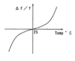
そこでこれらの問題を解決したものが、本出願人により出願された特開2001−60828に開示されている。これはMOS容量素子の本来有する曲線的な容量変化を利用した直接型TCXOである。以下に図を基にその原理を詳細に説明する。いま、図14に示す様な温度周波数特性をもった水晶発振器の温度補償を考える。これは、常温(基準温度:例えば25℃)以下の低温部においては周波数が曲線的に低下し、常温近傍において周波数の変位は小さく、常温以上の高温では周波数が曲線的に上昇するという3次関数曲線である。 A solution to these problems is disclosed in JP-A-2001-60828 filed by the present applicant. This is a direct TCXO utilizing a curved capacitance change inherent in a MOS capacitance element. The principle will be described below in detail with reference to the drawings. Now, consider temperature compensation of a crystal oscillator having a temperature frequency characteristic as shown in FIG. This is because the frequency decreases in a low-temperature part below normal temperature (reference temperature: 25 ° C.) in a curved manner, the frequency displacement is small near normal temperature, and the frequency increases in a curved manner in a high temperature above normal temperature. It is a function curve.
そこで図15に示すような容量変化を呈するMOS容量素子の特性に着目した。これはMOS容量素子のアノード電圧を基準としたゲート電圧(以下単にゲート電圧と称す)と、MOS容量素子の両端に現れる容量値との関係であり、ゲート電圧が低いVaにおいては容量値は高く、その変化は僅少でり、ゲート電圧が高くなるにつれ急減に減少し、Vbにおいて容量値は低く、その変化は僅少になる。ここで、MOS容量素子の容量特性は、変化傾斜がこれとは逆方向のものや、変化曲線が横軸方向に平行移動したもの等々種々のものが知られているので、これは一例である。今、同図の様にVa’からVaに向かってゲート電圧を変化させたとき、容量値は急激に増加し、ゲート電圧が低くなるに従って容量値は大きくその変化は僅少となる。この曲線部分を(A)とする。一方VbからVb’に向かってゲート電圧を変化させたとき、容量値は小さくその変化は僅少であったものが、ゲート電圧が低くなるに従って急激に大きくなる。この曲線部分を(B)とする。 Therefore, attention has been paid to the characteristics of the MOS capacitance element exhibiting a capacitance change as shown in FIG. This is a relationship between the gate voltage (hereinafter simply referred to as gate voltage) based on the anode voltage of the MOS capacitance element and the capacitance value appearing at both ends of the MOS capacitance element. , The change is small and decreases sharply as the gate voltage increases, and the capacitance value is low at Vb, and the change is small. Here, as the capacitance characteristics of the MOS capacitance element, various types are known, such as those having a change gradient in a direction opposite to this, and those having a change curve parallel-translated in the horizontal axis direction. This is an example. . Now, when the gate voltage is changed from Va 'to Va as shown in the figure, the capacitance value sharply increases, and the capacitance value increases as the gate voltage decreases, and the change becomes small. This curved portion is referred to as (A). On the other hand, when the gate voltage is changed from Vb to Vb ', the capacitance value is small and the change is small, but increases rapidly as the gate voltage decreases. This curved portion is referred to as (B).
ここで前記特性をもつMOS容量素子を二つ使用し、低温から高温になるにつれ一方はゲート電圧をVa’からVaへ、他方はVbからVb’へと、夫々直線的に変化するよう加えた場合において、その両者の温度/容量値特性を重ね書きすると図15の様になる。そしてこの一方の曲線部分(A)を低温部補償回路として、また他方の曲線部分(B)を高温部補償回路として、夫々発振回路の負荷容量の一部に組込めば、図14に示す3次関数曲線の温度特性をもつ水晶振動子の温度補償が可能となる。 Here, two MOS capacitors having the above characteristics were used, and one was added so that as the temperature increased from low to high, one changed the gate voltage from Va ′ to Va, and the other changed linearly from Vb to Vb ′, respectively. In this case, when the temperature / capacitance value characteristics of the two are overwritten, the result is as shown in FIG. If one of the curve portions (A) is incorporated as a low-temperature portion compensation circuit and the other curve portion (B) is incorporated as a high-temperature portion compensation circuit in a part of the load capacitance of the oscillation circuit, the circuit shown in FIG. The temperature compensation of the crystal unit having the temperature characteristic of the following function curve can be performed.
以下にこのMOS容量素子を利用した温度温度補償回路の例をもとにその動作について説明する。図17は増幅器に水晶振動子とMOS容量素子を用いた高温部補償回路と低温部補償回路とを直列に接続したものである。高温用MOS容量素子MHと低温用MOS容量素子MLとは共に同一極性の向きに直列接続され、また低温用MOS容量素子MLには感度調整用固定容量素子Cf1が直列に、高温用MOS容量素子MHには感度調整用固定容量素子Cf2が並列に接続されている。そして前記二つのMOS容量素子には入力抵抗Rを介して温度補償制御電圧信号VL、VHが温度センサと制御回路とから供給され、前記二つのMOS容量素子の接続点には入力抵抗Rを介して基準電圧信号Vrefが供給されるように構成されている。 The operation will be described below based on an example of a temperature / temperature compensation circuit using this MOS capacitance element. FIG. 17 shows a configuration in which a high-temperature part compensation circuit and a low-temperature part compensation circuit using a crystal unit and a MOS capacitor for an amplifier are connected in series. The high-temperature MOS capacitor MH and the low-temperature MOS capacitor ML are both connected in series in the same polarity direction, and the low-temperature MOS capacitor ML includes a sensitivity adjustment fixed capacitor Cf1 connected in series, and the high-temperature MOS capacitor A fixed capacitance element for sensitivity adjustment Cf2 is connected in parallel to MH. Then, temperature compensation control voltage signals VL and VH are supplied from the temperature sensor and the control circuit to the two MOS capacitors via an input resistor R, and a connection point between the two MOS capacitors is connected via an input resistor R. Thus, the reference voltage signal Vref is supplied.
この補償回路において、温度が低温から高温まで変化するのに対応して、低温用MOS容量素子MLのアノード電圧を基準としたゲート電圧をVa’からVaへ、また高温用MOS容量素子MHのアノード電圧を基準としたゲート電圧をVbからVb’へと直線的に変化させることを考える。するとここでは、低温用MOS容量素子MLのゲート端子にはVrefが供給されているので、アノード端子には(Vref−Va’)から(Vref−Va)へと直線的に増加する制御電圧信号VLを供給し、一方高温用MOS容量素子MHのアノード端子にはVrefが供給されているので、ゲート端子には(Vref+Vb)から(Vref+Vb’)へと直線的に減少する制御電圧信号VHを供給する。 すると、前記図15のに示す温度/容量特性曲線(A)及び(B)の直列合成容量が発振ループに挿入される事になり、図14に示すような3次関数曲線を有する水晶振動子の温度補償をすることが可能となる。 In this compensation circuit, in response to the temperature change from low to high, the gate voltage based on the anode voltage of the low-temperature MOS capacitor ML is changed from Va ′ to Va, and the anode of the high-temperature MOS capacitor MH is changed. Consider that the gate voltage based on the voltage is linearly changed from Vb to Vb '. Then, here, since Vref is supplied to the gate terminal of the low-temperature MOS capacitive element ML, the control voltage signal VL that linearly increases from (Vref−Va ′) to (Vref−Va) is supplied to the anode terminal. On the other hand, since Vref is supplied to the anode terminal of the high-temperature MOS capacitive element MH, a control voltage signal VH that linearly decreases from (Vref + Vb) to (Vref + Vb ′) is supplied to the gate terminal. . Then, the series combined capacitance of the temperature / capacitance characteristic curves (A) and (B) shown in FIG. 15 is inserted into the oscillation loop, and the crystal unit having a cubic function curve as shown in FIG. Can be compensated for.
ここで、感度調整用固定容量素子Cf1、Cf2は夫々の補償特性曲線形状を任意に設定出来る様に自由度を与えたものであり、これは直並列の合成容量値の性質を利用したものである。いま低温部補償回路において、例えば常温における固定容量素子Cf1と低温用MOS容量素子MLとの値がほぼ同じ場合を想定し、この直列合成容量値の振る舞いを検討する。MOS容量素子の値は、低温から常温にかけて小さい値から増加し、常温及び常温以上の温度において大きくなる。よってこの直列合成容量値は、低温においてMOS容量素子の値の変化が支配的となり、一方常温及び常温以上の温度においてはMOS容量素子の値は大きくなるので、この直列合成容量値は、固定容量素子の値に制限されてその変化は僅少となる。これとは逆に、高温部補償回路においては、常温における固定容量素子Cf2と高温用MOS容量素子MHとの値がほぼ同じ場合を想定すると、MOS容量素子の値が低温から常温にかけて小さい値のとき、固定容量素子の値が支配的でその変化は僅少となり、常温以上の温度においてMOS容量素子の値が大きくなるにつれ、MOS容量素子の変化が支配的となる。この様な性質を利用して夫々の感度調整用固定容量素子Cf1、Cf2の値を調整すれば、より水晶振動子の曲線に適合した温度補償容量曲線を得ることが可能となる。 Here, the sensitivity adjustment fixed capacitance elements Cf1 and Cf2 are provided with a degree of freedom so that the shape of each compensation characteristic curve can be set arbitrarily, and this utilizes the property of the series-parallel combined capacitance value. is there. Now, in the low-temperature part compensation circuit, for example, it is assumed that the value of the fixed capacitance element Cf1 at room temperature and the value of the low-temperature MOS capacitance element ML are almost the same, and the behavior of this series combined capacitance value will be examined. The value of the MOS capacitor increases from a small value from a low temperature to a normal temperature, and increases at a normal temperature and a temperature higher than the normal temperature. Therefore, in the series combined capacitance value, the change in the value of the MOS capacitor becomes dominant at a low temperature, and the value of the MOS capacitor becomes large at a normal temperature and a temperature higher than the normal temperature. The change is limited by the value of the element. Conversely, in the high temperature section compensation circuit, assuming that the value of the fixed capacitance element Cf2 and the value of the high temperature MOS capacitance element MH at room temperature are almost the same, the value of the MOS capacitance element becomes smaller from low temperature to room temperature. At this time, the value of the fixed capacitance element is dominant and its change is small. At a temperature higher than the normal temperature, the change of the MOS capacitance element becomes dominant as the value of the MOS capacitance element increases. By adjusting the values of the fixed capacitance elements Cf1 and Cf2 for sensitivity adjustment using such properties, it is possible to obtain a temperature compensation capacitance curve that is more suited to the curve of the crystal resonator.
以上説明したように、この原理を用いれば、従来の間接型補償と比較した場合、水晶振動子の3次曲線補償のためにこれに近似した制御電圧信号を生成すること無く、単に直線的な温度/電圧信号を発生すればよいので、補償回路が極めて簡単になる。またC/N特性においては、制御電圧信号にデジタル信号を含まないことと、最も使用頻度の高い常温近辺において発振ループ中に含まれるMOS容量素子の電圧感度をほとんどゼロに設定できるので、極めて良好な特性となる。また従来の直接型補償と比較した場合は、IC化が容易に可能となることによる小型化のメリットは勿論のこと、発振ループ中にサーミスタの抵抗成分を含まないので、水晶振動子の良好なQ値をそのまま維持できる為、更にC/N特性を良好に保つことが可能であり、また発振維持に必要な消費電力を少なくできる上、温度による出力レベルの変動もない。この様にMOS容量素子を利用した直接型温度補償方式は、従来の間接型補償、直接型補償方式に比較して何重もの利点を有する。
そこで、現在最も優れた温度補償方式と考えられる特開2001−60828に開示された補償原理を利用し、更なる小型化・ローコスト化を追求し、発振器としてもより多くの要求仕様に対応できる具体的な回路構成が望まれていた。 Therefore, by utilizing the compensation principle disclosed in Japanese Patent Application Laid-Open No. 2001-60828, which is considered to be the most excellent temperature compensation method at present, further miniaturization and cost reduction are pursued, and the oscillator can cope with more required specifications. There has been a demand for a specific circuit configuration.
上記課題を解決する為に請求項1に記載の発明は、圧電発振器の発振ループ中に挿入接続して周波数温度補償を行うための周波数温度補償回路であって、該周波数温度補償回路は、第1のMOS容量素子のアノード端子に固定容量素子の一方端子を接続した直列回路と第2のMOS容量素子とを該第2のMOS容量素子のアノード端子が前記第1のMOS容量素子のゲート端子と接続するように並列接続した並列回路であり、前記第1のMOS容量素子のゲート端子と前記第2のMOS容量素子のアノード端子との接続点に電圧値が一定である基準電圧信号を供給し、前記第1のMOS容量素子のアノード端子に第1の制御電圧信号を供給し、前記第2のMOS容量素子のゲート端子に第2の制御電圧信号を供給する構成を備えていることを特徴としている。
In order to solve the above-mentioned problem, the invention according to
請求項2に記載の発明は、発振回路と、直流阻止用固定容量素子と、周波数温度補償回路と、圧電振動子と、を直列に接続した構造の温度補償発振器であって、前記周波数温度補償回路が、第1のMOS容量素子のアノード端子に固定容量素子の一方端子を接続した直列回路と第2のMOS容量素子とを該第2のMOS容量素子のアノード端子が前記第1のMOS容量素子のゲート端子と接続するように並列接続した並列回路であり、前記第1のMOS容量素子のゲート端子と前記第2のMOS容量素子のアノード端子との接続点に電圧値が一定である基準電圧信号を供給し、前記第1のMOS容量素子のアノード端子に第1の制御電圧信号を供給し、前記第2のMOS容量素子のゲート端子に第2の制御電圧信号を供給する構成を備えていることを特徴としている。 According to a second aspect of the present invention, there is provided a temperature compensated oscillator having a structure in which an oscillation circuit, a DC blocking fixed capacitance element, a frequency temperature compensation circuit, and a piezoelectric vibrator are connected in series. A circuit includes a series circuit in which one terminal of a fixed capacitance element is connected to an anode terminal of a first MOS capacitance element, and a second MOS capacitance element. The anode terminal of the second MOS capacitance element has an anode terminal of the first MOS capacitance. A parallel circuit connected in parallel so as to be connected to a gate terminal of the element, wherein a reference voltage having a constant voltage value is provided at a connection point between the gate terminal of the first MOS capacitor and the anode terminal of the second MOS capacitor; A voltage signal is supplied, a first control voltage signal is supplied to an anode terminal of the first MOS capacitance element, and a second control voltage signal is supplied to a gate terminal of the second MOS capacitance element. And It is characterized in that.
請求項3に記載の発明は、コルピッツ発振回路と、周波数温度補償回路と、圧電振動子と、を直列に接続した構造の温度補償発振器であって、前記周波数温度補償回路が、第1のMOS容量素子のアノード端子に固定容量素子の一方端子を接続した直列回路と第2のMOS容量素子とを該第2のMOS容量素子のアノード端子が前記第1のMOS容量素子のゲート端子と接続するように並列接続した並列回路であり、前記第1のMOS容量素子のゲート端子と前記第2のMOS容量素子のアノード端子との接続点に電圧値が一定である基準電圧信号を供給し、前記第1のMOS容量素子のアノード端子に第1の制御電圧信号を供給し、前記第2のMOS容量素子のゲート端子に第2の制御電圧信号を供給する構成を備えたものであるか、或いは、前記周波数温度補償回路が、第1のMOS容量素子のアノード端子に固定容量素子の一方端子を接続した直列回路と、第2のMOS容量素子と固定容量素子との並列回路とを前記第1のMOS容量素子のゲート端子と前記第2のMOS容量素子のアノード端子とが接続するように直列接続した直列回路であり、前記第1のMOS容量素子のゲート端子と前記第2のMOS容量素子のアノード端子との接続点に電圧値が一定である基準電圧信号を供給し、前記第1のMOS容量素子のアノード端子に第1の制御電圧信号を供給し、前記第2のMOS容量素子のゲート端子に第2の制御電圧信号を供給する構成を備えたものであり、前記コルピッツ発振回路が、トランジスタと、該トランジスタのベースにバイアス電圧を供給する為のバイアス回路とを少なくとも備えており、前記トランジスタのベースとバイアス回路との接続点と、接地に一方端子が接続された2つの固定容量素子からなる直列回路の他方端子との間に直流阻止用固定容量素子を挿入接続した構成であって、前記2つの固定容量素子からなる直列回路と前記直流阻止用固定容量素子との接続点が、前記周波数温度補償回路と接続されていることを特徴としている。 According to a third aspect of the present invention, there is provided a temperature compensation oscillator having a structure in which a Colpitts oscillation circuit, a frequency temperature compensation circuit, and a piezoelectric vibrator are connected in series, wherein the frequency temperature compensation circuit comprises a first MOS transistor. A series circuit in which one terminal of a fixed capacitance element is connected to the anode terminal of the capacitance element and a second MOS capacitance element are connected with the anode terminal of the second MOS capacitance element being connected to the gate terminal of the first MOS capacitance element. And a reference voltage signal having a constant voltage value is supplied to a connection point between a gate terminal of the first MOS capacitance element and an anode terminal of the second MOS capacitance element. A first control voltage signal is supplied to an anode terminal of the first MOS capacitance element, and a second control voltage signal is supplied to a gate terminal of the second MOS capacitance element; or I The frequency temperature compensation circuit includes a series circuit in which one terminal of a fixed capacitance element is connected to an anode terminal of a first MOS capacitance element, and a parallel circuit of a second MOS capacitance element and a fixed capacitance element. A series circuit in which the gate terminal of the first MOS capacitor and the anode terminal of the second MOS capacitor are connected in series, wherein the gate terminal of the first MOS capacitor and the second MOS capacitor are connected. A reference voltage signal having a constant voltage value is supplied to a connection point with the anode terminal of the first MOS capacitor, a first control voltage signal is supplied to the anode terminal of the first MOS capacitor, The Colpitts oscillation circuit includes a transistor and a via for supplying a bias voltage to a base of the transistor. A fixed circuit for direct current blocking between a connection point between the base of the transistor and a bias circuit and the other terminal of a series circuit including two fixed capacitance elements each having one terminal connected to the ground. An element is inserted and connected, and a connection point between the series circuit composed of the two fixed capacitance elements and the DC blocking fixed capacitance element is connected to the frequency temperature compensation circuit.
請求項4に記載の発明は、発振回路と、周波数温度補償回路と、圧電振動子と、を直列に接続した構造の温度補償発振器であって、前記発振回路が、トランジスタと、該トランジスタのベースにバイアス電圧を供給する為のバイアス回路とを少なくとも備えており、前記周波数温度補償回路が、第1のMOS容量素子のアノード端子に固定容量素子の一方端子を接続した直列回路と第2のMOS容量素子とを該第2のMOS容量素子のアノード端子が前記第1のMOS容量素子のゲート端子と接続するように並列接続した並列回路であり、前記第1のMOS容量素子のアノード端子に第1の制御電圧信号を供給し、前記第2のMOS容量素子のゲート端子に第2の制御電圧信号を供給する構成を備えたものであり、前記第1のMOS容量素子のゲート端子と前記第2のMOS容量素子のアノード端子との接続点に前記発振回路を構成する前記バイアス回路のバイアス電圧信号を供給するように構成したことを特徴としている。 The invention according to claim 4 is a temperature-compensated oscillator having a structure in which an oscillation circuit, a frequency temperature compensation circuit, and a piezoelectric vibrator are connected in series, wherein the oscillation circuit comprises a transistor and a base of the transistor. And a bias circuit for supplying a bias voltage to the first MOS capacitor, wherein the frequency temperature compensation circuit includes a series circuit in which one terminal of the fixed capacitor is connected to the anode terminal of the first MOS capacitor, and a second MOS transistor. A capacitor connected in parallel so that an anode terminal of the second MOS capacitor is connected to a gate terminal of the first MOS capacitor; and a second circuit connected to the anode terminal of the first MOS capacitor. A first control voltage signal, and a second control voltage signal to a gate terminal of the second MOS capacitance element. It is characterized by being configured to provide a bias voltage signal of the bias circuit constituting the oscillator circuit to a connection point between the gate terminal and the anode terminal of the second MOS capacitance element.
請求項5に記載の発明は、発振回路と、周波数温度補償回路と、圧電振動子と、周波数外部電圧制御回路と、を直列に接続した構造の温度補償発振器であって、前記周波数温度補償回路が、第1のMOS容量素子のアノード端子に固定容量素子の一方端子を接続した直列回路と第2のMOS容量素子とを該第2のMOS容量素子のアノード端子が前記第1のMOS容量素子のゲート端子と接続するように並列接続した並列回路であり、前記第1のMOS容量素子のゲート端子と前記第2のMOS容量素子のアノード端子との接続点に電圧値が一定である基準電圧信号を供給し、前記第1のMOS容量素子のアノード端子に第1の制御電圧信号を供給し、前記第2のMOS容量素子のゲート端子に第2の制御電圧信号を供給する構成を備えたものであるか、或いは、前記周波数温度補償回路が、第1のMOS容量素子のアノード端子に第1の固定容量素子の一方端子を接続した直列回路と、第2のMOS容量素子と第2の固定容量素子との並列回路とを前記第1のMOS容量素子のゲート端子と前記第2のMOS容量素子のアノード端子とが接続するように直列接続した直列回路であり、前記第1のMOS容量素子のゲート端子と前記第2のMOS容量素子のアノード端子との接続点に電圧値が一定である基準電圧信号を供給し、前記第1のMOS容量素子のアノード端子に第1の制御電圧信号を供給し、前記第2のMOS容量素子のゲート端子に第2の制御電圧信号を供給する構成を備えたものであり、前記周波数外部電圧制御回路が、MOS容量素子のゲート端子に外部制御電圧信号を供給する構成、或いはMOS容量素子のゲート端子に外部制御電圧信号を供給すると共にアノード端子に電圧値が一定である基準電圧信号を供給する構成からなることを特徴としている。 The invention according to claim 5 is a temperature compensation oscillator having a structure in which an oscillation circuit, a frequency temperature compensation circuit, a piezoelectric vibrator, and a frequency external voltage control circuit are connected in series, wherein the frequency temperature compensation circuit Is a series circuit in which one terminal of a fixed capacitance element is connected to the anode terminal of a first MOS capacitance element and a second MOS capacitance element. The anode terminal of the second MOS capacitance element is connected to the first MOS capacitance element. And a reference voltage having a constant voltage value at a connection point between the gate terminal of the first MOS capacitance element and the anode terminal of the second MOS capacitance element. A first control voltage signal is supplied to an anode terminal of the first MOS capacitor, and a second control voltage signal is supplied to a gate terminal of the second MOS capacitor. Also Alternatively, the frequency temperature compensation circuit may include a series circuit in which one terminal of the first fixed capacitance element is connected to the anode terminal of the first MOS capacitance element, and a second fixed capacitance element connected to the second fixed capacitance element. A series circuit in which a parallel circuit with a capacitor is connected in series so that a gate terminal of the first MOS capacitor and an anode terminal of the second MOS capacitor are connected; A reference voltage signal having a constant voltage value is supplied to a connection point between the gate terminal of the first MOS capacitor and the anode terminal of the second MOS capacitor, and a first control voltage signal is supplied to the anode terminal of the first MOS capacitor. And a second control voltage signal is supplied to a gate terminal of the second MOS capacitance element. The frequency external voltage control circuit is configured to supply an external control voltage to a gate terminal of the MOS capacitance element. And supplied the item, or the voltage value to the anode terminal is supplied an external control voltage signal to the gate terminal of the MOS capacitor element is characterized by comprising a structure for supplying a reference voltage signal is constant.
請求項6に記載の発明は、発振回路と、周波数外部電圧制御回路と、固定容量素子と、周波数温度補償回路と、圧電振動子と、を直列に接続した構造の温度補償発振器であって、前記発振回路が、トランジスタと、該トランジスタのベースにバイアス電圧を供給する為のバイアス回路とを少なくとも備えており、前記周波数温度補償回路が、第1のMOS容量素子のアノード端子に固定容量素子の一方端子を接続した直列回路と第2のMOS容量素子とを該第2のMOS容量素子のアノード端子が前記第1のMOS容量素子のゲート端子と接続するように並列接続した並列回路であり、前記第1のMOS容量素子のゲート端子と前記第2のMOS容量素子のアノード端子との接続点に電圧値が一定である基準電圧信号を供給し、前記第1のMOS容量素子のアノード端子に第1の制御電圧信号を供給し、前記第2のMOS容量素子のゲート端子に第2の制御電圧信号を供給する構成を備えたものであるか、或いは、前記周波数温度補償回路が、第1のMOS容量素子のアノード端子に第1の固定容量素子の一方端子を接続した直列回路と、第2のMOS容量素子と第2の固定容量素子との並列回路とを前記第1のMOS容量素子のゲート端子と前記第2のMOS容量素子のアノード端子とが接続するように直列接続した直列回路であり、前記第1のMOS容量素子のゲート端子と前記第2のMOS容量素子のアノード端子との接続点に電圧値が一定である基準電圧信号を供給し、前記第1のMOS容量素子のアノード端子に第1の制御電圧信号を供給し、前記第2のMOS容量素子のゲート端子に第2の制御電圧信号を供給する構成を備えたものであり、前記周波数外部電圧制御回路が、MOS容量素子のゲート端子に外部制御電圧信号を供給し、アノード端子に前記発振回路に接続することにより前記トランジスタのバイアス電圧信号を供給したことを特徴としている。 The invention according to claim 6 is a temperature compensated oscillator having a structure in which an oscillation circuit, a frequency external voltage control circuit, a fixed capacitance element, a frequency temperature compensation circuit, and a piezoelectric vibrator are connected in series, The oscillation circuit includes at least a transistor and a bias circuit for supplying a bias voltage to a base of the transistor. The frequency temperature compensation circuit includes a fixed capacitance element connected to an anode terminal of the first MOS capacitance element. A parallel circuit in which a series circuit having one terminal connected thereto and a second MOS capacitor are connected in parallel such that an anode terminal of the second MOS capacitor is connected to a gate terminal of the first MOS capacitor; A reference voltage signal having a constant voltage value is supplied to a connection point between the gate terminal of the first MOS capacitor and the anode terminal of the second MOS capacitor, and the first M A configuration in which a first control voltage signal is supplied to an anode terminal of the S capacitance element and a second control voltage signal is supplied to a gate terminal of the second MOS capacitance element; The temperature compensation circuit includes a series circuit in which one terminal of the first fixed capacitance element is connected to an anode terminal of the first MOS capacitance element, and a parallel circuit of the second MOS capacitance element and the second fixed capacitance element. A series circuit in which the gate terminal of the first MOS capacitor and the anode terminal of the second MOS capacitor are connected in series so that the gate terminal of the first MOS capacitor is connected to the second terminal of the second MOS capacitor. A reference voltage signal having a constant voltage value is supplied to a connection point of the MOS capacitor with an anode terminal, a first control voltage signal is supplied to an anode terminal of the first MOS capacitor, and the second MOS Capacitive element A configuration for supplying a second control voltage signal to a gate terminal, wherein the frequency external voltage control circuit supplies an external control voltage signal to a gate terminal of a MOS capacitor, and an anode terminal to the oscillation circuit. The connection is characterized in that a bias voltage signal of the transistor is supplied.
請求項7に記載の発明は、発振回路と、固定容量素子と、周波数温度補償回路と周波数外部電圧制御回路とを並列接続した並列回路又は該周波数温度補償回路と該周波数外部電圧制御回路とを直列接続した直列回路と、圧電振動子と、を直列に接続した構造の温度補償発振器であって、前記周波数温度補償回路が、第1のMOS容量素子のアノード端子に固定容量素子の一方端子を接続した直列回路と第2のMOS容量素子とを該第2のMOS容量素子のアノード端子が前記第1のMOS容量素子のゲート端子と接続するように並列接続した並列回路であり、前記第1のMOS容量素子のゲート端子と前記第2のMOS容量素子のアノード端子との接続点に電圧値が一定である基準電圧信号を供給し、前記第1のMOS容量素子のアノード端子に第1の制御電圧信号を供給し、前記第2のMOS容量素子のゲート端子に第2の制御電圧信号を供給する構成を備えたものであり、前記周波数外部電圧制御回路が、MOS容量素子のゲート端子に外部制御電圧信号を供給し、アノード端子に前記周波数温度補償回路の前記第1のMOS容量素子のゲート端子と前記第2のMOS容量素子のアノード端子との接続点を接続することにより、前記周波数温度補償回路の前記基準電圧信号を供給したことを特徴としている。 According to a seventh aspect of the present invention, there is provided an oscillation circuit, a fixed capacitance element, a parallel circuit in which a frequency temperature compensation circuit and a frequency external voltage control circuit are connected in parallel, or a frequency temperature compensation circuit and the frequency external voltage control circuit. A temperature-compensated oscillator having a structure in which a series circuit connected in series and a piezoelectric vibrator are connected in series, wherein the frequency temperature compensation circuit connects one terminal of the fixed capacitance element to an anode terminal of the first MOS capacitance element. A parallel circuit in which the connected series circuit and the second MOS capacitor are connected in parallel such that the anode terminal of the second MOS capacitor is connected to the gate terminal of the first MOS capacitor; A reference voltage signal having a constant voltage value is supplied to a connection point between the gate terminal of the first MOS capacitor and the anode terminal of the second MOS capacitor. And a second control voltage signal is supplied to a gate terminal of the second MOS capacitance element, and the frequency external voltage control circuit comprises a MOS capacitance element. An external control voltage signal is supplied to the gate terminal of the frequency temperature compensation circuit, and a connection point between the gate terminal of the first MOS capacitance element and the anode terminal of the second MOS capacitance element is connected to the anode terminal. Wherein the reference voltage signal of the frequency temperature compensation circuit is supplied.
請求項8に記載の発明は、発振回路と、周波数温度補償回路と周波数外部電圧制御回路とを並列接続した並列回路と、圧電振動子と、を直列に接続した構造の温度補償発振器であって、前記発振回路が、トランジスタと、該トランジスタのベースにバイアス電圧を供給する為のバイアス回路とを少なくとも備えており、前記周波数温度補償回路が、第1のMOS容量素子のアノード端子に固定容量素子の一方端子を接続した直列回路と第2のMOS容量素子とを該第2のMOS容量素子のアノード端子が前記第1のMOS容量素子のゲート端子と接続するように並列接続した並列回路であり、前記第1のMOS容量素子のアノード端子に第1の制御電圧信号を供給し、前記第2のMOS容量素子のゲート端子に第2の制御電圧信号を供給する構成を備えたものであり、前記周波数外部電圧制御回路が、MOS容量素子のゲート端子に外部制御電圧信号を供給し、アノード端子に前記周波数温度補償回路の前記第1のMOS容量素子のゲート端子と前記第2のMOS容量素子のアノード端子との接続点を接続し、更に、該接続点を前記発振回路に接続することにより前記トランジスタのバイアス電圧信号を供給したことを特徴としている。 The invention according to claim 8 is a temperature compensated oscillator having a structure in which an oscillation circuit, a parallel circuit in which a frequency temperature compensation circuit and a frequency external voltage control circuit are connected in parallel, and a piezoelectric vibrator are connected in series. The oscillation circuit includes at least a transistor and a bias circuit for supplying a bias voltage to the base of the transistor, and the frequency temperature compensation circuit includes a fixed capacitance element connected to an anode terminal of the first MOS capacitance element. And a second MOS capacitor connected in parallel so that an anode terminal of the second MOS capacitor is connected to a gate terminal of the first MOS capacitor. Supplying a first control voltage signal to an anode terminal of the first MOS capacitance element and supplying a second control voltage signal to a gate terminal of the second MOS capacitance element The frequency external voltage control circuit supplies an external control voltage signal to a gate terminal of a MOS capacitance element, and an anode terminal of the gate terminal of the first MOS capacitance element of the frequency temperature compensation circuit. And a connection point between the transistor and the anode terminal of the second MOS capacitance element, and the connection point is connected to the oscillation circuit to supply a bias voltage signal for the transistor.
請求項9に記載の発明は、コルピッツ発振回路と、圧電振動子と、周波数温度補償回路と、固定容量素子と、を直列に接続した構造の温度補償発振器であって、前記周波数温度補償回路は、第1のMOS容量素子のアノード端子に固定容量素子の一方端子を接続した直列回路と第2のMOS容量素子とを該第2のMOS容量素子のアノード端子が前記第1のMOS容量素子のゲート端子と接続するように並列接続した並列回路であり、前記第1のMOS容量素子のゲート端子と前記第2のMOS容量素子のアノード端子との接続点に電圧値が一定である基準電圧信号を供給し、前記第1のMOS容量素子のアノード端子に第1の制御電圧信号を供給し、前記第2のMOS容量素子のゲート端子に第2の制御電圧信号を供給する構成を備えたものであるか、或いは、前記周波数温度補償回路が、第1のMOS容量素子のアノード端子に第1の固定容量素子の一方端子を接続した直列回路と、第2のMOS容量素子と第2の固定容量素子との並列回路とを前記第1のMOS容量素子のゲート端子と前記第2のMOS容量素子のアノード端子とが接続するように直列接続した直列回路であり、前記第1のMOS容量素子のゲート端子と前記第2のMOS容量素子のアノード端子との接続点に電圧値が一定である基準電圧信号を供給し、前記第1のMOS容量素子のアノード端子に第1の制御電圧信号を供給し、前記第2のMOS容量素子のゲート端子に第2の制御電圧信号を供給する構成を備えたものであり、前記コルピッツ発振回路が、トランジスタのベースとエミッタとの間に接続された第1の容量回路と、前記エミッタとアースとの間に接続された第2の容量回路とを少なくとも備えており、前記第1の容量回路がMOS容量素子を備え、該MOS容量素子のゲート端子に制御電圧信号を供給することによって、前記第1の容量回路の容量値が可変できることを特徴としている。 The invention according to claim 9 is a temperature compensation oscillator having a structure in which a Colpitts oscillation circuit, a piezoelectric vibrator, a frequency temperature compensation circuit, and a fixed capacitance element are connected in series, wherein the frequency temperature compensation circuit is A series circuit in which one terminal of a fixed capacitance element is connected to the anode terminal of the first MOS capacitance element and a second MOS capacitance element, the anode terminal of the second MOS capacitance element being connected to the anode terminal of the first MOS capacitance element A reference voltage signal having a constant voltage value at a connection point between a gate terminal of the first MOS capacitor and an anode terminal of the second MOS capacitor, which is a parallel circuit connected in parallel so as to be connected to a gate terminal. And a first control voltage signal is supplied to an anode terminal of the first MOS capacitance element, and a second control voltage signal is supplied to a gate terminal of the second MOS capacitance element. Alternatively, the frequency temperature compensation circuit may include a series circuit in which one terminal of the first fixed capacitance element is connected to the anode terminal of the first MOS capacitance element, and a second fixed capacitance element connected to the second fixed capacitance element. A series circuit in which a parallel circuit with a capacitor is connected in series so that a gate terminal of the first MOS capacitor and an anode terminal of the second MOS capacitor are connected; A reference voltage signal having a constant voltage value is supplied to a connection point between the gate terminal of the first MOS capacitor and the anode terminal of the second MOS capacitor, and a first control voltage signal is supplied to the anode terminal of the first MOS capacitor. And a second control voltage signal supplied to the gate terminal of the second MOS capacitance element, wherein the Colpitts oscillation circuit is connected between the base and the emitter of the transistor. A first capacitance circuit, and a second capacitance circuit connected between the emitter and the ground, the first capacitance circuit including a MOS capacitance element, and a gate of the MOS capacitance element. By supplying a control voltage signal to the terminal, the capacitance value of the first capacitance circuit can be varied.
請求項10に記載の発明は、コルピッツ発振回路と、周波数温度補償回路と、圧電振動子と、を直列に接続した構造の温度補償発振器であって、前記周波数温度補償回路は、第1のMOS容量素子のアノード端子に固定容量素子の一方端子を接続した直列回路と第2のMOS容量素子とを該第2のMOS容量素子のアノード端子が前記第1のMOS容量素子のゲート端子と接続するように並列接続した並列回路であり、前記第1のMOS容量素子のゲート端子と前記第2のMOS容量素子のアノード端子との接続点に電圧値が一定である基準電圧信号を供給し、前記第1のMOS容量素子のアノード端子に第1の制御電圧信号を供給し、前記第2のMOS容量素子のゲート端子に第2の制御電圧信号を供給する構成を備えたものであるか、或いは、前記周波数温度補償回路が、第1のMOS容量素子のアノード端子に第1の固定容量素子の一方端子を接続した直列回路と、第2のMOS容量素子と第2の固定容量素子との並列回路とを前記第1のMOS容量素子のゲート端子と前記第2のMOS容量素子のアノード端子とが接続するように直列接続した直列回路であり、前記第1のMOS容量素子のゲート端子と前記第2のMOS容量素子のアノード端子との接続点に電圧値が一定である基準電圧信号を供給し、前記第1のMOS容量素子のアノード端子に第1の制御電圧信号を供給し、前記第2のMOS容量素子のゲート端子に第2の制御電圧信号を供給する構成を備えたものであり、前記コルピッツ発振回路が、トランジスタのベースとエミッタとの間に接続された第1の容量回路と、前記エミッタとアースとの間に接続された第2の容量回路とを少なくとも備えており、前記第2の容量回路がMOS容量素子を備え、該MOS容量素子のゲート端子に制御電圧信号を供給することによって、前記第1の容量回路の容量値が可変できることを特徴としている。 An invention according to claim 10 is a temperature compensation oscillator having a structure in which a Colpitts oscillation circuit, a frequency temperature compensation circuit, and a piezoelectric vibrator are connected in series, wherein the frequency temperature compensation circuit comprises a first MOS transistor. A series circuit in which one terminal of a fixed capacitance element is connected to the anode terminal of the capacitance element and a second MOS capacitance element are connected with the anode terminal of the second MOS capacitance element being connected to the gate terminal of the first MOS capacitance element. And a reference voltage signal having a constant voltage value is supplied to a connection point between a gate terminal of the first MOS capacitance element and an anode terminal of the second MOS capacitance element. A first control voltage signal is supplied to an anode terminal of the first MOS capacitance element, and a second control voltage signal is supplied to a gate terminal of the second MOS capacitance element; or The frequency temperature compensation circuit comprises a series circuit in which one terminal of the first fixed capacitance element is connected to the anode terminal of the first MOS capacitance element, and a second MOS capacitance element and a second fixed capacitance element. A series circuit in which a parallel circuit is connected in series so that a gate terminal of the first MOS capacitor and an anode terminal of the second MOS capacitor are connected; Supplying a reference voltage signal having a constant voltage value to a connection point of the second MOS capacitance element with the anode terminal, supplying a first control voltage signal to the anode terminal of the first MOS capacitance element, A second control voltage signal is supplied to a gate terminal of a second MOS capacitance element, and the Colpitts oscillation circuit includes a first capacitance connected between a base and an emitter of the transistor. And a second capacitor circuit connected between the emitter and the ground, the second capacitor circuit including a MOS capacitor, and a control voltage signal connected to a gate terminal of the MOS capacitor. Is supplied, the capacitance value of the first capacitance circuit can be varied.
請求項11に記載の発明は、請求項1乃至10のいずれかに記載の温度補償発振器であって、前記MOS容量素子のゲート端子とアノード端子とをすべて逆の極性に接続したことを特徴としている。 According to an eleventh aspect of the present invention, in the temperature compensated oscillator according to any one of the first to tenth aspects, the gate terminal and the anode terminal of the MOS capacitor are all connected to opposite polarities. I have.
請求項12に記載の発明は、コルピッツ発振回路と、圧電振動子と、周波数温度補償回路と、固定容量素子と、を直列に接続した構造の温度補償発振器であって、前記周波数温度補償回路が、第1のMOS容量素子のアノード端子に固定容量素子を接続し、該第1のMOS容量素子のゲート端子には第2のMOS容量素子のアノード端子を接続した直列回路であり、前記第1のMOS容量素子のゲート端子と前記第2のMOS容量素子のアノード端子との接続点に電圧値が一定である基準電圧信号を供給し、前記第1のMOS容量素子のアノード端子に第1の制御電圧信号を供給し、前記第2のMOS容量素子のゲート端子に第2の制御電圧信号を供給する構成を備えたものであり、
前記コルピッツ発振回路が、トランジスタのベースとエミッタとの間に接続された第1の容量回路と、前記エミッタとアースとの間に接続された第2の容量回路とを少なくとも備えており、
前記第1の容量回路がMOS容量素子を利用した外部電圧制御回路を備え、該MOS容量素子のゲート端子に制御電圧信号を供給することによって、前記第1の容量回路の容量値が可変できることを特徴としている。
The invention according to claim 12 is a temperature-compensated oscillator having a structure in which a Colpitts oscillation circuit, a piezoelectric vibrator, a frequency temperature compensation circuit, and a fixed capacitance element are connected in series, wherein the frequency temperature compensation circuit is A fixed capacitance element is connected to an anode terminal of the first MOS capacitance element, and a gate terminal of the first MOS capacitance element is connected to an anode terminal of a second MOS capacitance element. A reference voltage signal having a constant voltage value is supplied to a connection point between the gate terminal of the MOS capacitance element and the anode terminal of the second MOS capacitance element, and the first voltage is supplied to the anode terminal of the first MOS capacitance element. A control voltage signal is supplied, and a second control voltage signal is supplied to a gate terminal of the second MOS capacitance element.
The Colpitts oscillation circuit includes at least a first capacitance circuit connected between the base and the emitter of the transistor, and a second capacitance circuit connected between the emitter and the ground,
The first capacitance circuit includes an external voltage control circuit using a MOS capacitance element, and a capacitance value of the first capacitance circuit can be varied by supplying a control voltage signal to a gate terminal of the MOS capacitance element. Features.
請求項13に記載の発明は、コルピッツ発振回路と、周波数温度補償回路と、圧電振動子と、を直列に接続した構造の温度補償発振器であって、
前記周波数温度補償回路は、第1のMOS容量素子のアノード端子に固定容量素子の一方端子を接続した直列回路と第2のMOS容量素子とを該第2のMOS容量素子のアノード端子が前記第1のMOS容量素子のゲート端子と接続するように並列接続した並列回路であり、前記第1のMOS容量素子のゲート端子と前記第2のMOS容量素子のアノード端子との接続点に電圧値が一定である基準電圧信号を供給し、前記第1のMOS容量素子のアノード端子に第1の制御電圧信号を供給し、前記第2のMOS容量素子のゲート端子に第2の制御電圧信号を供給する構成を備えたものであり、
前記コルピッツ発振回路が、トランジスタのベースとエミッタとの間に接続された第1の容量回路と、前記エミッタとアースとの間に接続された第2の容量回路とを少なくとも備えており、
前記第2の容量回路がMOS容量素子を利用した外部電圧制御回路を備え、該MOS容量素子のゲート端子に制御電圧信号を供給することによって、前記第1の容量回路の容量値が可変できることを特徴としている。
The invention according to claim 13 is a temperature-compensated oscillator having a structure in which a Colpitts oscillation circuit, a frequency temperature compensation circuit, and a piezoelectric vibrator are connected in series,
The frequency temperature compensation circuit includes a series circuit in which one terminal of a fixed capacitance element is connected to an anode terminal of a first MOS capacitance element, and a second MOS capacitance element. A parallel circuit is connected in parallel so as to be connected to the gate terminal of the first MOS capacitor, and a voltage value is applied to a connection point between the gate terminal of the first MOS capacitor and the anode terminal of the second MOS capacitor. A constant reference voltage signal is supplied, a first control voltage signal is supplied to an anode terminal of the first MOS capacitance element, and a second control voltage signal is supplied to a gate terminal of the second MOS capacitance element. It has a configuration to
The Colpitts oscillation circuit includes at least a first capacitance circuit connected between the base and the emitter of the transistor, and a second capacitance circuit connected between the emitter and the ground,
The second capacitance circuit may include an external voltage control circuit using a MOS capacitance element, and a capacitance value of the first capacitance circuit may be varied by supplying a control voltage signal to a gate terminal of the MOS capacitance element. Features.
請求項14に記載の発明は、コルピッツ発振回路と、周波数温度補償回路と、圧電振動子と、を直列に接続した構造の温度補償発振器であって、前記周波数温度補償回路が、第1のMOS容量素子のアノード端子に固定容量素子を接続し、該第1のMOS容量素子のゲート端子には第2のMOS容量素子のアノード端子を接続した直列回路であり、前記第1のMOS容量素子のゲート端子と前記第2のMOS容量素子のアノード端子との接続点に電圧値が一定である基準電圧信号を供給し、前記第1のMOS容量素子のアノード端子に第1の制御電圧信号を供給し、前記第2のMOS容量素子のゲート端子に第2の制御電圧信号を供給する構成を備えたものであり、
前記コルピッツ発振回路が、トランジスタのベースとエミッタとの間に接続された第1の容量回路と、前記エミッタとアースとの間に接続された第2の容量回路とを少なくとも備えており、
前記第2の容量回路がMOS容量素子を利用した外部電圧制御回路を備え、該MOS容量素子のゲート端子に制御電圧信号を供給することによって、前記第1の容量回路の容量値が可変できることを特徴としている。
An invention according to claim 14 is a temperature compensated oscillator having a structure in which a Colpitts oscillation circuit, a frequency temperature compensation circuit, and a piezoelectric vibrator are connected in series, wherein the frequency temperature compensation circuit comprises a first MOS transistor. A series circuit in which a fixed capacitance element is connected to an anode terminal of the capacitance element, and a gate terminal of the first MOS capacitance element is connected to an anode terminal of a second MOS capacitance element. A reference voltage signal having a constant voltage value is supplied to a connection point between a gate terminal and an anode terminal of the second MOS capacitance element, and a first control voltage signal is supplied to an anode terminal of the first MOS capacitance element. And providing a second control voltage signal to a gate terminal of the second MOS capacitance element.
The Colpitts oscillation circuit includes at least a first capacitance circuit connected between the base and the emitter of the transistor, and a second capacitance circuit connected between the emitter and the ground,
The second capacitance circuit may include an external voltage control circuit using a MOS capacitance element, and a capacitance value of the first capacitance circuit may be varied by supplying a control voltage signal to a gate terminal of the MOS capacitance element. Features.
請求項15に記載の発明は、前記周波数温度補償回路を構成する各MOS容量素子のうち第1のMOS容量素子には直列に固定容量素子を、また第2のMOS容量素子には並列に固定容量素子を接続したことを特徴としている。 According to a fifteenth aspect of the present invention, of the MOS capacitors constituting the frequency temperature compensation circuit, a fixed capacitor is fixed in series to the first MOS capacitor, and fixed in parallel to the second MOS capacitor. It is characterized in that a capacitance element is connected.
請求項16に記載の発明は、前記周波数温度補償回路を構成する各MOS容量素子の極性をいずれも逆としたことを特徴としている。 The invention according to claim 16 is characterized in that the polarity of each of the MOS capacitors constituting the frequency temperature compensation circuit is reversed.
請求項17に記載の発明は、前記周波数外部電圧制御回路又は、外部電圧制御回路を構成するMOS容量素子の極性を逆としたことを特徴とする請求項5乃至14のいずれかに記載の温度補償発振器。 According to a seventeenth aspect of the present invention, the polarity of the frequency external voltage control circuit or the MOS capacitor constituting the external voltage control circuit is reversed. Compensated oscillator.
請求項18に記載の発明は、圧電発振器の発振ループ中に挿入接続して周波数温度補償を行うための周波数温度補償回路であって、該周波数温度補償回路は、第1のMOS容量素子のアノード端子に固定容量素子の一方端子を接続した直列回路と第2のMOS容量素子とを該第2のMOS容量素子のアノード端子が前記第1のMOS容量素子のゲート端子と接続するように並列接続した並列回路であり、前記第1のMOS容量素子のゲート端子と前記第2のMOS容量素子のアノード端子との接続点に電圧値が一定である基準電圧信号を供給し、前記第1のMOS容量素子のアノード端子に第1の制御電圧信号を供給し、前記第2のMOS容量素子のゲート端子に第2の制御電圧信号を供給する構成を備えていることを特徴としている。 An invention according to claim 18 is a frequency temperature compensation circuit for performing frequency temperature compensation by being inserted into an oscillation loop of a piezoelectric oscillator, wherein the frequency temperature compensation circuit comprises an anode of a first MOS capacitive element. A series circuit in which one terminal of a fixed capacitance element is connected to a terminal and a second MOS capacitance element are connected in parallel such that the anode terminal of the second MOS capacitance element is connected to the gate terminal of the first MOS capacitance element. And supplying a reference voltage signal having a constant voltage value to a connection point between a gate terminal of the first MOS capacitance element and an anode terminal of the second MOS capacitance element. The first control voltage signal is supplied to the anode terminal of the capacitor and the second control voltage signal is supplied to the gate terminal of the second MOS capacitor.
請求項19に記載の発明は、前記周波数温度補償回路を構成する各MOS容量素子の極性をいずれも逆としたことを特徴としている。 The invention according to claim 19 is characterized in that the polarity of each of the MOS capacitors constituting the frequency temperature compensation circuit is reversed.
請求項20に記載の発明は、前記周波数温度補償回路と直列に1次温度補償用可変容量素子を接続し、温度に対して直線的に電圧が変化する1次温度補償電圧源からの電圧を前記1次温度補償用可変容量素子に対して印加したことを特徴している。 According to a twentieth aspect of the present invention, a primary temperature compensating variable capacitance element is connected in series with the frequency temperature compensating circuit, and a voltage from a primary temperature compensating voltage source whose voltage changes linearly with temperature is supplied. The voltage is applied to the primary temperature compensating variable capacitance element.
以上説明したように、特開2001−60828に開示された補償原理を利用した温度補償発振器において、更なる小型化・ローコスト化を追求しつつ、MOS容量素子利用した様々な回路構成を提案することにより、より多くの要求仕様に対応できる温度補償発振器の実現を可能とした。 As described above, in the temperature compensated oscillator using the compensation principle disclosed in Japanese Patent Application Laid-Open No. 2001-60828, various circuit configurations using MOS capacitance elements are proposed while pursuing further miniaturization and lower cost. As a result, it has become possible to realize a temperature-compensated oscillator that can meet more required specifications.
以下、図示した実施例に基づいて本発明を詳細に説明する。
図1は、本発明の第一の実施例を示す回路図である。この例に示すTCXOは、コルピッツ発振回路Os1に、直流阻止用固定容量素子C3と、温度補償回路Co1と、水晶振動子Xとを直列に接続したもので、典型的なコルピッツ型水晶発振器に本発明を適用したものである。
Hereinafter, the present invention will be described in detail with reference to the illustrated embodiments.
FIG. 1 is a circuit diagram showing a first embodiment of the present invention. The TCXO shown in this example has a Colpitts oscillation circuit Os1, a DC blocking fixed capacitance element C3, a temperature compensation circuit Co1, and a crystal unit X connected in series. It is an application of the invention.
このコルピッツ発振回路Os1は、発振増幅用トランジスタTR1のコレクタは電源に接続され、バイパスコンデンサCcを介して高周波的に接地され、ベースには抵抗R1、R2によって適宜バイアスされており、ベースとエミッタ間に第一の固定容量素子C1が接続されると共に、エミッタと接地間にはエミッタ抵抗Reと第二の固定容量素子C2とが並列接続され、発振出力は前記エミッタから直流阻止用固定容量素子Coを介して取り出すように構成されている。更に、前記トランジスタTR1のベースには直流阻止用固定容量素子C3を介して温度補償回路Co1と水晶振動子Xが接続されている。
この温度補償回路Co1は、低温部補償用MOS容量素子MLと感度調整用固定容量素子C4との直列接続回路と、高温部補償用MOS容量素子MHとの並列接続からなっており、低温用MOS容量素子MLと高温用MOS容量素子MHが互いに異なる極性の向きとなっている。
In the Colpitts oscillation circuit Os1, the collector of the oscillation amplification transistor TR1 is connected to a power supply, grounded at a high frequency via a bypass capacitor Cc, and the base is appropriately biased by resistors R1 and R2. , A first fixed capacitor C1 is connected, an emitter resistor Re and a second fixed capacitor C2 are connected in parallel between the emitter and the ground, and the oscillation output is supplied from the emitter to the DC blocking fixed capacitor Co. Is configured to be taken out through the device. Further, a temperature compensating circuit Co1 and a crystal resonator X are connected to the base of the transistor TR1 via a DC blocking fixed capacitance element C3.
The temperature compensation circuit Co1 is composed of a series connection circuit of a low-temperature part compensation MOS capacitance element ML and a sensitivity adjustment fixed capacitance element C4, and a parallel connection of a high-temperature part compensation MOS capacitance element MH. The capacitance element ML and the high-temperature MOS capacitance element MH have different polarities.
また、低温用MOS容量素子MLのアノード端子側と固定容量素子C4との接続中点には、低温部制御電圧信号VLが入力抵抗R4を介して供給されていて、高温用MOS容量素子MHのゲート端子側には入力抵抗R5を介して高温部制御電圧信号VHが供給されている。そして、この低温用MOS容量素子MLのゲート端子側と高温用MOS容量素子MHのアノード端子側には基準電圧信号Vrefが入力抵抗R6を介して供給されている。 Further, a low-temperature section control voltage signal VL is supplied via an input resistor R4 to a connection point between the anode terminal side of the low-temperature MOS capacitance element ML and the fixed capacitance element C4. The high-temperature section control voltage signal VH is supplied to the gate terminal via the input resistor R5. A reference voltage signal Vref is supplied to the gate terminal of the low-temperature MOS capacitor ML and the anode terminal of the high-temperature MOS capacitor MH via the input resistor R6.
このコルピッツ発振回路Os1の動作については既に周知であるから説明を省略し、本発明の特徴である温度補償回路Co1について詳細に説明する。MOS容量素子の特性を温度補償回路に利用する原理は、前述の従来技術でべた通りであり、この実施例は従来例にくらべて、各補償回路を並列にした点と、感度調整用固定容量素子C4を低温部補償用と高温部補償用とを共通にしたことにより1つ削除した点が異なる。 Since the operation of the Colpitts oscillation circuit Os1 is already well known, a description thereof will be omitted, and the temperature compensation circuit Co1, which is a feature of the present invention, will be described in detail. The principle of using the characteristics of the MOS capacitance element for the temperature compensation circuit is as described in the above-mentioned conventional technology. This embodiment is different from the conventional example in that the compensation circuits are arranged in parallel and the sensitivity adjustment fixed capacitor is used. The element C4 is different in that the element C4 is commonly used for the low-temperature part compensation and the high-temperature part compensation.
まず、各補償回路を直列に接続した場合と並列に接続した場合との違いについて説明する。直並列の合成容量値の性質を考えると、複数の容量素子を直列接続した場合には小さい容量値の変化が支配的となり、並列接続した場合には大きい容量値の変化が支配的となることは周知の通りである。よって、前記従来技術で説明した図15の様な容量特性をもつMOS容量素子を使用した場合、ほとんどの温度範囲において低温部補償回路の容量値が高温部補償回路の容量値より大きいので、これらを直列に接続した場合は高温部補償回路の容量変化が大きく影響し、よって補償回路全体として高温部の補償感度が大きくなる傾向を示す。また逆にこれらを並列に接続した場合は、低温部補償回路の容量変化が大きく影響し、低温部の補償感度が大きくなる傾向を示す。
しかしここで、補償回路全体の負荷容量を一定とした場合は、低温部補償回路と高温部補償回路とを並列に接続すると、各補償回路の容量値を小さく設計できることになる。よって直列に接続した場合に比べ、夫々のMOS容量素子の容量値、及び感度調整用固定容量素子の値を小さく設計できるのでICの小型化が可能となる。また感度調整用固定容量素子C4は、低温部補償用MOS容量素子MLに対しては直列に、また高温部補償用MOS容量素子MHに対しては並列に接続されているので、前述の従来技術で説明した低温部と高温部における感度調整を1つの容量素子で同時に行うことができる。この為IC化する際に最も占有面積の大きい固定容量素子を1つ削除することができ、更なるICの小型化が可能となる。
更に又、MOS容量素子は制御電圧信号に重畳される交流成分の振幅に比例して電圧可変感度が劣化してしまうという特性をもつ。ここで各補償回路を並列に接続し交流成分を分流した場合、夫々のMOS容量素子の各制御電圧信号に重畳される交流成分の振幅は下がることになる為、夫々のMOS容量素子の電圧可変感度の劣化を緩和することが可能となる。
First, the difference between the case where each compensation circuit is connected in series and the case where they are connected in parallel will be described. Considering the nature of the series-parallel combined capacitance value, a small change in capacitance value is dominant when multiple capacitive elements are connected in series, and a large change in capacitance value is dominant when connected in parallel. Is well known. Therefore, when the MOS capacitance element having the capacitance characteristic as shown in FIG. 15 described in the prior art is used, the capacitance value of the low-temperature part compensation circuit is larger than that of the high-temperature part compensation circuit in most of the temperature range. Are connected in series, the change in capacitance of the high-temperature portion compensation circuit has a large effect, and therefore, the compensation sensitivity of the high-temperature portion tends to increase as the whole compensation circuit. Conversely, when these are connected in parallel, the change in capacitance of the low-temperature section compensation circuit has a large effect, and the low-temperature section compensation sensitivity tends to increase.
However, if the load capacitance of the entire compensation circuit is constant, connecting the low-temperature part compensation circuit and the high-temperature part compensation circuit in parallel makes it possible to design the capacitance value of each compensation circuit to be small. Accordingly, the capacitance value of each MOS capacitance element and the value of the sensitivity adjustment fixed capacitance element can be designed to be smaller than the case where they are connected in series, so that the size of the IC can be reduced. The fixed capacitance element C4 for sensitivity adjustment is connected in series to the low-temperature part compensation MOS capacitance element ML and connected in parallel to the high-temperature part compensation MOS capacitance element MH. The sensitivity adjustment in the low-temperature part and the high-temperature part described in (1) can be performed simultaneously by one capacitance element. For this reason, it is possible to eliminate one fixed capacitance element having the largest occupied area when forming an IC, and it is possible to further reduce the size of the IC.
Further, the MOS capacitance element has a characteristic that the voltage variable sensitivity deteriorates in proportion to the amplitude of the AC component superimposed on the control voltage signal. Here, when the compensating circuits are connected in parallel to shunt the AC component, the amplitude of the AC component superimposed on each control voltage signal of each MOS capacitor decreases, so that the voltage of each MOS capacitor changes. Deterioration of sensitivity can be alleviated.
ここで増幅器のバイアス回路は、ここでは電流帰還型の固定バイアス回路を例に説明したが、これに限らず自己バイアス回路や単なる固定バイアス回路を用いても、そしてカスコード型としても良く、またインバーター発振回路を使用しても良い。また前述の様に、各MOS容量素子ML、MHはその特性が逆のもの存在するので、これらの極性の向きは共に逆であっても良い。またここで、水晶振動子Xと固定容量素子C3の配置を入換えても、また温度補償回路Co1の向きを逆にしてもこの温度補償回路の効果は変らない。 Here, the bias circuit of the amplifier has been described by taking a current feedback type fixed bias circuit as an example, but the present invention is not limited to this, and a self-bias circuit or a simple fixed bias circuit may be used, and a cascode type may be used. An oscillation circuit may be used. As described above, since the MOS capacitors ML and MH have the opposite characteristics, the polarities thereof may be reversed. Here, even if the arrangement of the crystal unit X and the fixed capacitance element C3 is exchanged, or the direction of the temperature compensation circuit Co1 is reversed, the effect of this temperature compensation circuit does not change.
図2(A)は本発明の第二の実施例を示す回路図であり、コルピッツ発振回路Os2に、温度補償回路Co1と、水晶振動子Xとを直列に接続したものである。この温度補償回路Co1は第一の実施例で説明したものと同様の、並列接続の温度補償回路である。またこの回路図は第一の実施例に比べて、直流阻止用固定容量素子C3の位置が異なる。すなわち、前記コルピッツ発振回路Os1を構成するトランジスタTR1のベースに接続されたバイアス抵抗R1とR2との接続点1と、この接続点1より温度補償回路Co1側に設けた、固定容量素子C1と前記ベースとの接続点2との間に、前記直流阻止用、すなわちベースバイアスと前記温度補償回路Coに供給された各制御電圧信号の直流成分とを阻止する為の固定容量素子C3を挿入したものである。(簡単のため、以下この直流阻止用固定容量素子C3を含めてコルピッツ発振回路Os2と称す。)
この様に固定容量素子C3を発振ループの中の負荷容量から外すことで、温度補償回路Co1の補償感度は増加し、全体の負荷容量を小さく設計できるのでICの小型化が可能となる。
この固定容量素子C3は、前述の様にトランジスタTR1のベースとバイアス抵抗との接続点1とベースと固定容量素子C1との接続点2との間に挿入するので、前記トランジスタTR1のベースとエミッタ間の容量Cbcに直列に接続されることになる。ここで、固定容量素子C3は発振信号を増幅器に入力する為に出来るだけ大きい値が好ましいが、ICの小型化を考慮して現在数十pF程度を想定している。一方このCbcは通常数pFと小さい値であるので、C3とCbcとの直列合成容量値も小さな値となる。よってこれらと並列に接続されている固定容量素子C1への影響は非常に小さい。
またこの効果はこの例に限らず、図2(A)中の温度補償回路Co1を、図2(B)に示すような、従来技術で説明した直列温度補償回路とした場合においても同様の効果があり、また後述する外部制御回路等を付加した場合において、各制御電圧信号等の直流信号分を阻止するための固定容量素子を接続する必要性がある回路構成において有効である。
FIG. 2A is a circuit diagram showing a second embodiment of the present invention, in which a temperature compensation circuit Co1 and a crystal resonator X are connected in series to a Colpitts oscillation circuit Os2. This temperature compensation circuit Co1 is a parallel connection temperature compensation circuit similar to that described in the first embodiment. In this circuit diagram, the position of the DC blocking fixed capacitance element C3 is different from that of the first embodiment. That is, a
By thus removing the fixed capacitance element C3 from the load capacitance in the oscillation loop, the compensation sensitivity of the temperature compensation circuit Co1 increases, and the overall load capacitance can be designed to be small, so that the IC can be downsized.
Since the fixed capacitance element C3 is inserted between the
This effect is not limited to this example, and the same effect can be obtained when the temperature compensation circuit Co1 in FIG. 2A is replaced with the series temperature compensation circuit described in the related art as shown in FIG. 2B. In addition, when an external control circuit or the like to be described later is added, it is effective in a circuit configuration in which it is necessary to connect a fixed capacitance element for blocking a DC signal component such as each control voltage signal.
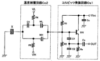
図3は本発明の第三の実施例を示す回路図であり、コルピッツ発振回路Os1に、温度補償回路Co2と、水晶振動子Xとを直列に接続したものである。
この温度補償回路Co1は、低温部補償用MOS容量素子MLと感度調整用固定容量素子C4との直列接続回路と、高温部補償用MOS容量素子MHとの並列接続からなっており、低温用MOS容量素子MLと高温用MOS容量素子MHが互いに異なる極性の向きとなっている。
また、低温用MOS容量素子MLのアノード端子側と固定容量素子C4との接続中点には、低温部制御電圧信号VLが入力抵抗R4を介して供給されていて、高温用MOS容量素子MHのゲート端子側には入力抵抗R5を介して高温部制御電圧信号VHが供給されている。ここでこの温度補償回路Co2の低温用MOS容量素子MLのゲート端子と高温用MOS容量素子MHのアノード端子との接続点を、コルピッツ発振回路Os1の入力となるトランジスタTR1のベースに接続することにより、基準電圧信号を供給している。これは第一の実施例に比べて、電圧値が一定である基準電圧信号Vrefの値を前記トランジスタTR1のベースバイアスに設定することにより、基準電圧信号Vrefと直流阻止用固定容量素子C3とを削除した点が異なる。(以下簡単の為に、基準電圧信号Vrefを削除し、直流阻止用固定容量素子C3を必要としないこの温度補償回路を、温度補償回路Co2と称す。)これにより補償電圧信号発生回路の簡素化及び省電力化、そしてICの小型化が可能となり、また固定容量素子C3をなくしたことによるICの小型化の効果も大きい。
FIG. 3 is a circuit diagram showing a third embodiment of the present invention, in which a temperature compensation circuit Co2 and a crystal resonator X are connected in series to a Colpitts oscillation circuit Os1.
The temperature compensation circuit Co1 is composed of a series connection circuit of a low-temperature part compensation MOS capacitance element ML and a sensitivity adjustment fixed capacitance element C4, and a parallel connection of a high-temperature part compensation MOS capacitance element MH. The capacitance element ML and the high-temperature MOS capacitance element MH have different polarities.
Further, a low-temperature section control voltage signal VL is supplied via an input resistor R4 to a connection point between the anode terminal side of the low-temperature MOS capacitance element ML and the fixed capacitance element C4. The high-temperature section control voltage signal VH is supplied to the gate terminal via the input resistor R5. Here, the connection point between the gate terminal of the low-temperature MOS capacitance element ML and the anode terminal of the high-temperature MOS capacitance element MH of the temperature compensation circuit Co2 is connected to the base of the transistor TR1 which is the input of the Colpitts oscillation circuit Os1. , And a reference voltage signal. This is different from the first embodiment in that the value of the reference voltage signal Vref having a constant voltage value is set as the base bias of the transistor TR1, thereby allowing the reference voltage signal Vref and the DC blocking fixed capacitance element C3 to be connected to each other. The difference is that they have been deleted. (Hereinafter, for simplicity, the reference voltage signal Vref is deleted, and this temperature compensation circuit that does not require the DC blocking fixed capacitance element C3 is referred to as a temperature compensation circuit Co2.) This simplifies the compensation voltage signal generation circuit. In addition, power saving and downsizing of the IC become possible, and the effect of downsizing the IC due to the elimination of the fixed capacitance element C3 is great.
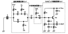
図4は本発明の第四の実施例を示す回路図であり、コルピッツ発振回路Os1に、直流阻止用固定容量素子C3と、温度補償回路Co1と、水晶振動子Xと、外部制御回路Vc1とを直列に接続したものである。この外部制御回路Vc1はMOS容量素子MAのゲート端子側に入力抵抗R7を介して外部制御電圧信号Vafcを供給すると共に、水晶振動子Xと接続し、一方のアノード端子側は接地している。これは第一の実施例に比べて、外部制御回路Vc1を付加した点が異なり、MOS容量素子MAの高可変感度で直線性の優れた電圧/容量特性を利用すれば、直線性の優れた周波数外部可変が可能となる。(又は直線性の優れたAFC:Automatic Frequency Control機能を付加したともいえる。)またこの外部制御回路Vc1は図5(A)に示す外部制御回路Vc2ように、前記MOS容量素子のアノード電極に入力抵抗R8を介して基準電圧信号Varefを供給し調整することにより、このMOS容量素子MAの容量特性の任意の曲線部分を周波数制御に利用することが可能となり、各MOS容量素子MAの曲線の製造誤差を補正することも可能となる。更にまた、この外部制御回路Vc1及びVc2の構成を並列に接続したものを利用すれば、より精度よく周波数調整を行うことができるので、中心周波数の微調整なども可能となる。ここで、ICの製作工程においては固定容量素子の製作よりもMOS容量素子の製作の方が容易であるので、外部制御回路Vc1及びVc2の両端子に供給する制御電圧信号を夫々一定電圧とするか、又は一方端子を一定電圧とし他方端子を接地することにより、MOS容量素子MAを固定容量素子として利用することも出来る。また、図4中の温度補償回路Co1を、図2(B)に示すような従来技術で説明した直列温度補償回路とした場合においても前述と同様の効果がある。 FIG. 4 is a circuit diagram showing a fourth embodiment of the present invention. The Colpitts oscillation circuit Os1 includes a DC blocking fixed capacitance element C3, a temperature compensation circuit Co1, a crystal oscillator X, an external control circuit Vc1, Are connected in series. The external control circuit Vc1 supplies an external control voltage signal Vafc to the gate terminal side of the MOS capacitive element MA via the input resistor R7, is connected to the crystal oscillator X, and has one anode terminal side grounded. This is different from the first embodiment in that an external control circuit Vc1 is added. If the voltage / capacity characteristics of the MOS variable element MA with high variable sensitivity and excellent linearity are used, excellent linearity can be obtained. Frequency external variable becomes possible. (Or it can be said that an AFC: Automatic Frequency Control function with excellent linearity is added.) Further, this external control circuit Vc1 is connected to the anode electrode of the MOS capacitor element like the external control circuit Vc2 shown in FIG. By supplying and adjusting the reference voltage signal Varef via the resistor R8, it is possible to use an arbitrary curve portion of the capacitance characteristic of the MOS capacitance element MA for frequency control, and to manufacture the curve of each MOS capacitance element MA. It is also possible to correct the error. Furthermore, if the configuration in which the external control circuits Vc1 and Vc2 are connected in parallel is used, the frequency can be adjusted more accurately, so that the center frequency can be finely adjusted. Here, in the manufacturing process of the IC, it is easier to manufacture the MOS capacitance element than to manufacture the fixed capacitance element. Therefore, the control voltage signals supplied to both terminals of the external control circuits Vc1 and Vc2 are each set to a constant voltage. Alternatively, by setting one terminal to a constant voltage and grounding the other terminal, the MOS capacitance element MA can be used as a fixed capacitance element. Further, even when the temperature compensation circuit Co1 in FIG. 4 is the series temperature compensation circuit described in the related art as shown in FIG.
図6は本発明の第五の実施例を示す回路図であり、コルピッツ発振回路Os1に、外部制御回路Vc1と、直流阻止用固定容量素子C5と、温度補償回路Co1と、水晶振動子Xとを直列に接続したものである。これはMOS容量素子MAのアノード端子に基準電圧信号としてトランジスタTR1のベースバイアスを供給したもので、外部制御回路Vc2の様な調整機能を有したうえで、基準電圧信号Varefと直流阻止用固定容量素子C3を削除する効果がある。また、図5中の温度補償回路Co1を、図2(B)に示すような従来技術で説明した直列温度補償回路とした場合においても前述と同様の効果がある。更にここで、この構成の水晶振動子Xの両端に印可される電圧に注目すると、前記第4の実施例の図4においては、この水晶振動子Xの両端に温度補償回路の基準電圧信号Vrefと外部制御電圧信号Vafcとが印可されている。この外部制御電圧信号Vafcの電圧は客先での使用時に個別に設定される為に、水晶振動子Xの両端に印加される電圧は設計時には決定されない。一方この第五の実施例の図6(及び前述の図1、図2)の場合、温度補償回路の基準電圧信号Vrefと接地との間に水晶振動子Xが挿入されている。ここで前記基準電圧信号数Vrefが数Vに設定されていると仮定すると、このTCXOの電源投入時には水晶振動子Xの両端には数Vの電圧がかかることになり、これは初期振動子電流を増加させ、しいては発振回路の起動特性を早くする効果、及び外部制御電圧信号Vafcの値によらず常に安定させるという効果がある。この効果はこの例に限らず、発振回路と、温度補償回路と、水晶振動子と、外部制御回路とを、直流信号が互いに干渉しない範囲において、水晶振動子の両端にかかる電圧が電源投入時に高く、そして安定した値となるように並べて構成すれば良い。例えば、この温度補償回路の高温部制御電圧信号VHと低温部制御電圧信号VLとは、常温近辺の温度範囲においてほぼ0Vとなる様に設定したとする。一方図5(A)に示す外部制御回路Vc2の基準電圧信号Varefは数Vとなる様に設計した場合においては、この高温部制御電圧信号VH又は低温部制御電圧信号VLと外部制御回路Vc2の基準電圧信号Varefとの間に水晶振動子Xが挿入される様な回路配置にすれば、常温近辺の温度範囲において前述と同様の効果が期待できる。 FIG. 6 is a circuit diagram showing a fifth embodiment of the present invention. In the Colpitts oscillation circuit Os1, an external control circuit Vc1, a DC blocking fixed capacitance element C5, a temperature compensation circuit Co1, a quartz oscillator X Are connected in series. This supplies the base bias of the transistor TR1 as a reference voltage signal to the anode terminal of the MOS capacitance element MA, and has an adjustment function like the external control circuit Vc2. There is an effect of eliminating the element C3. Further, even when the temperature compensation circuit Co1 in FIG. 5 is the series temperature compensation circuit described in the related art as shown in FIG. Attention is now paid to the voltage applied to both ends of the crystal unit X having this configuration. In FIG. 4 of the fourth embodiment, the reference voltage signal Vref of the temperature compensation circuit is applied to both ends of the crystal unit X. And an external control voltage signal Vafc are applied. Since the voltage of the external control voltage signal Vafc is individually set at the time of use at the customer, the voltage applied to both ends of the crystal unit X is not determined at the time of design. On the other hand, in the case of FIG. 6 of the fifth embodiment (and FIGS. 1 and 2 described above), the crystal resonator X is inserted between the reference voltage signal Vref of the temperature compensation circuit and the ground. Here, assuming that the reference voltage signal number Vref is set to several volts, a voltage of several volts is applied to both ends of the crystal oscillator X when the power supply of the TCXO is turned on. Has the effect of increasing the start-up characteristics of the oscillation circuit, and has the effect of always being stabilized irrespective of the value of the external control voltage signal Vafc. This effect is not limited to this example, and the oscillation circuit, the temperature compensation circuit, the crystal unit, and the external control circuit are connected to each other when the voltage applied to both ends of the crystal unit is turned on within a range where the DC signals do not interfere with each other. What is necessary is just to arrange so that it may become a high and stable value. For example, it is assumed that the high-temperature part control voltage signal VH and the low-temperature part control voltage signal VL of this temperature compensation circuit are set to be almost 0 V in a temperature range near room temperature. On the other hand, when the reference voltage signal Varef of the external control circuit Vc2 shown in FIG. 5A is designed to be several volts, the high-temperature section control voltage signal VH or the low-temperature section control voltage signal VL and the external control circuit Vc2 If the circuit arrangement is such that the crystal resonator X is inserted between the reference voltage signal Varef and the reference voltage signal Varef, the same effect as described above can be expected in a temperature range near room temperature.
図7は本発明の第六の実施例を示す回路図であり、コルピッツ発振回路Os1に、直流阻止用固定容量素子C3と、温度補償回路Co1と、外部制御回路Vc2と、水晶振動子Xとを直列に接続したものである。このコルピッツ発振回路Os1と、外部制御回路Vc2と、温度補償回路Co1の構成は前述の通りであるが、外部制御回路Vc2のMOS容量素子MAのアノード電極は、温度補償回路Co1のMOS容量素子MLのゲート電極とMHのアノード電極との接続点に接続することにより、温度補償回路Co1の基準電圧信号Vrefを供給していて、一方のMOS容量素子MAのゲート端子には入力抵抗R7を介して制御電圧信号Vafcが供給され、水晶振動子Xに接続されている。これは第四の実施例に比べて、外部制御回路Vc2の基準電圧信号Varefを、温度補償回路Co1の基準電圧信号Vrefに調整し、共通化したことが異なる。これにより、外部制御回路又は温度補償回路に供給する基準電圧信号を一つ削除することが可能となる。 FIG. 7 is a circuit diagram showing a sixth embodiment of the present invention. In the Colpitts oscillation circuit Os1, a DC blocking fixed capacitance element C3, a temperature compensation circuit Co1, an external control circuit Vc2, a quartz oscillator X Are connected in series. The configurations of the Colpitts oscillation circuit Os1, the external control circuit Vc2, and the temperature compensation circuit Co1 are as described above. The anode electrode of the MOS capacitance element MA of the external control circuit Vc2 is connected to the MOS capacitance element ML of the temperature compensation circuit Co1. The reference voltage signal Vref of the temperature compensation circuit Co1 is supplied by connecting to the connection point between the gate electrode of the MH and the anode electrode of the MH. The control voltage signal Vafc is supplied and connected to the crystal unit X. This is different from the fourth embodiment in that the reference voltage signal Varef of the external control circuit Vc2 is adjusted to the reference voltage signal Vref of the temperature compensation circuit Co1 and shared. This makes it possible to delete one reference voltage signal supplied to the external control circuit or the temperature compensation circuit.
図8は本発明の第七の実施例を示す回路図であり、コルピッツ発振回路Os1に、外部制御回路Vc1と直流阻止用固定容量素子C5との直列接続回路と、温度補償回路Co2との並列接続した回路を接続し、更に水晶振動子Xとを直列に接続したものである。この外部制御回路Vc1と温度補償回路Co2の構成は前述の通りであり、外部制御回路Vc1のMOS容量素子MAのアノード電極は、温度補償回路Co2のMOS容量素子MLのゲート電極とMHのアノード電極との接続点に接続し、更にコルピッツ発振回路Os1の入力となるトランジスタTR1のベースと接続している。これは、前記温度補償回路Co2の基準電圧信号Vrefと、外部制御回路Vc1の基準電圧信号Varefとを、共にトランジスタTR1のベースバイアスに等しく調整することにより可能となる。この構成により、温度補償回路Co2と外部制御回路Vc1の二つの基準電圧信号と、二つの直流阻止用固定容量素子を削除することが可能となる。またこの構成は、前記第四、第五の実施例の様に外部制御回路Vc1を温度補償回路Co2と直列に接続する場合と比較して、発振ループ全体の負荷容量値を下げる効果があり、結果としてこの温度補償回路Co2と外部制御回路Vc1の各MOS容量素子と固定容量素子の値を下げることができ、ICの小型化が可能となる。更に又、第一の実施例で説明したように、夫々の回路を並列接続することで、夫々のMOS容量素子に流れる交流成分が分流される結果、夫々の制御電圧信号に重畳される交流成分の振幅は下がることになる為、夫々のMOS容量素子の電圧可変感度の劣化を緩和することが可能となる。またここでは、前記温度補償回路Co2と前記外部制御回路Vc1との並列回路で説明したが、前記温度補償回路Co2は図2(B)に示す直列補償回路としても、また前記外部制御回路Vc1を前記外部制御回路Vc2としても、前述の並列接続による効果、すなわち発振ループ全体の負荷容量値を下げる効果と、夫々のMOS容量素子の電圧可変感度の劣化を緩和する効果がある。 FIG. 8 is a circuit diagram showing a seventh embodiment of the present invention. In the Colpitts oscillation circuit Os1, a series connection circuit of an external control circuit Vc1 and a DC blocking fixed capacitance element C5, and a temperature compensation circuit Co2 are connected in parallel. The connected circuits are connected, and a crystal resonator X is further connected in series. The configurations of the external control circuit Vc1 and the temperature compensation circuit Co2 are as described above. The anode electrode of the MOS capacitance element MA of the external control circuit Vc1 is connected to the gate electrode of the MOS capacitance element ML of the temperature compensation circuit Co2 and the anode electrode of the MH. , And further connected to the base of a transistor TR1 which is an input of the Colpitts oscillation circuit Os1. This is made possible by adjusting both the reference voltage signal Vref of the temperature compensation circuit Co2 and the reference voltage signal Varef of the external control circuit Vc1 to be equal to the base bias of the transistor TR1. With this configuration, it is possible to eliminate the two reference voltage signals of the temperature compensation circuit Co2 and the external control circuit Vc1, and the two DC blocking fixed capacitance elements. This configuration has the effect of lowering the load capacitance value of the entire oscillation loop as compared with the case where the external control circuit Vc1 is connected in series with the temperature compensation circuit Co2 as in the fourth and fifth embodiments. As a result, the values of the MOS capacitors and fixed capacitors of the temperature compensation circuit Co2 and the external control circuit Vc1 can be reduced, and the size of the IC can be reduced. Further, as described in the first embodiment, by connecting the respective circuits in parallel, the AC components flowing through the respective MOS capacitance elements are shunted, so that the AC components superimposed on the respective control voltage signals are obtained. Is reduced, it is possible to alleviate the deterioration of the voltage variable sensitivity of each MOS capacitor. Also, here, the parallel circuit of the temperature compensation circuit Co2 and the external control circuit Vc1 has been described. However, the temperature compensation circuit Co2 may be a series compensation circuit shown in FIG. The external control circuit Vc2 also has the effect of the above-described parallel connection, that is, the effect of reducing the load capacitance value of the entire oscillation loop, and the effect of alleviating the deterioration of the voltage variable sensitivity of each MOS capacitor.
図9(A)は本発明の第八の実施例を示す回路図であり、コルピッツ発振回路Os3、すなわち前記コルピッツ発振回路Os2の固定容量素子C1に代えて外部制御回路Vc1を構成するMOS容量素子MAを配置すると共に、水晶振動子Xと、温度補償回路Co1と、直流阻止用固定容量素子C5とを直列に接続したものである。コルピッツ発振回路Os3は前記第二の実施例で説明したコルピッツ発振回路Os2と同様に、直流阻止用固定容量素子C3が内部に組込まれている。またこの実施例では、第二の実施例で説明したコルピッツ発振回路の固定容量素子C1の代わりに、MOS容量素子MAをそのゲート電極が振動子Xと直流阻止用固定容量素子C3との接続中点に接続する向きに挿入されている。そしてこのゲート電極には入力抵抗R7を介して、外部制御電圧信号Vafcが供給されており、周波数の調整を可能とするとともに、このコルピッツ発振回路Os3の負性抵抗の調整を可能としている。これは異なる周波数帯の水晶振動子を同一のICで使用する際に有効な手段となる。一方このMOS容量素子MAのアノード電極はトランジスタTR1のエミッタに接続されているので、エミッタ電圧を調整することが可能な範囲において、このMOS容量素子MAの基準電圧を調整することができ、任意の容量特性曲線を利用することも可能である。また図9(B)は、同図(A)に示す温度補償回路Co1のVrefを0Vに設定し、低温部制御電圧信号VLと高温部制御電圧信号VHの接続点を接地した場合の図である。これにより固定容量素子C5、入力抵抗R6、そして基準電圧信号Vrefを削除することが可能となる。 FIG. 9A is a circuit diagram showing an eighth embodiment of the present invention, in which a Colpitts oscillation circuit Os3, that is, a MOS capacitance element forming an external control circuit Vc1 in place of the fixed capacitance element C1 of the Colpitts oscillation circuit Os2. The MA is arranged, and the crystal unit X, the temperature compensation circuit Co1, and the DC blocking fixed capacitance element C5 are connected in series. As in the Colpitts oscillation circuit Os2 described in the second embodiment, the Colpitts oscillation circuit Os3 has a DC blocking fixed capacitance element C3 incorporated therein. Further, in this embodiment, instead of the fixed capacitance element C1 of the Colpitts oscillation circuit described in the second embodiment, the MOS capacitance element MA is connected to the gate electrode between the resonator X and the DC blocking fixed capacitance element C3. Inserted in the direction to connect to the point. An external control voltage signal Vafc is supplied to the gate electrode via an input resistor R7, and the frequency can be adjusted and the negative resistance of the Colpitts oscillation circuit Os3 can be adjusted. This is an effective means when using quartz oscillators of different frequency bands in the same IC. On the other hand, since the anode electrode of this MOS capacitance element MA is connected to the emitter of transistor TR1, the reference voltage of this MOS capacitance element MA can be adjusted within the range in which the emitter voltage can be adjusted. It is also possible to use a capacitance characteristic curve. FIG. 9B is a diagram when Vref of the temperature compensation circuit Co1 shown in FIG. 9A is set to 0 V, and a connection point between the low-temperature section control voltage signal VL and the high-temperature section control voltage signal VH is grounded. is there. This makes it possible to eliminate the fixed capacitance element C5, the input resistance R6, and the reference voltage signal Vref.
図10は本発明の第九の実施例を示す回路図であり、コルピッツ発振回路Os4、すなわち前記コルピッツ発振回路Os2の固定容量素子C2に代えて外部制御回路Vc1を構成するMOS容量素子MAを配置すると共に、温度補償回路Co1と、水晶振動子Xとを直列に接続したものである。コルピッツ発振回路Os4は前記第二の実施例で説明したものと同様に、直流阻止用固定容量素子C3が内部に組込まれている。またこの実施例では、前記第二の実施例で説明したコルピッツ発振回路の固定容量素子C2の代わりに、MOS容量素子MAをそのアノード電極がトランジスタTR1のエミッタに接続する向きに挿入されている。そしてこのゲート電極には入力抵抗R7を介して、外部制御電圧信号Vafcが供給さるとともに、直流阻止用固定容量素子C5を介して接地されている。これは前記第八の実施例と同様の効果をもち、すなわち、周波数の調整を可能とするとともに、このコルピッツ発振回路Os2の負性抵抗の調整を可能としていて、異なる周波数帯の水晶振動子を同一のICで使用する際に有効な手段となる。またこの場合もMOS容量素子MAのアノード電極はトランジスタTR1のエミッタに接続されているので、エミッタ電圧を調整できる範囲において、MOS容量素子MAの基準電圧を調整すれば、任意の容量特性曲線を利用することも可能である。 FIG. 10 is a circuit diagram showing a ninth embodiment of the present invention, in which a Colpitts oscillation circuit Os4, that is, a MOS capacitance element MA constituting an external control circuit Vc1 is arranged in place of the fixed capacitance element C2 of the Colpitts oscillation circuit Os2. In addition, the temperature compensation circuit Co1 and the crystal resonator X are connected in series. As in the second embodiment, the Colpitts oscillation circuit Os4 has a DC blocking fixed capacitance element C3 incorporated therein. Further, in this embodiment, instead of the fixed capacitance element C2 of the Colpitts oscillation circuit described in the second embodiment, a MOS capacitance element MA is inserted so that its anode electrode is connected to the emitter of the transistor TR1. The gate electrode is supplied with an external control voltage signal Vafc via an input resistor R7 and is grounded via a DC blocking fixed capacitance element C5. This has the same effect as that of the eighth embodiment, that is, the frequency can be adjusted, and the negative resistance of the Colpitts oscillation circuit Os2 can be adjusted. This is an effective means when used with the same IC. Also in this case, since the anode electrode of the MOS capacitor MA is connected to the emitter of the transistor TR1, if the reference voltage of the MOS capacitor MA is adjusted within a range where the emitter voltage can be adjusted, an arbitrary capacitance characteristic curve can be used. It is also possible.
図11は本発明の第十の実施例を示す回路図であり、コルピッツ発振回路Os5、すなわち前記コルピッツ発振回路Os2の固定容量素子C2に代えて外部制御回路Vc1を構成するMOS容量素子MAを配置すると共に、温度補償回路Co1と、水晶振動子Xとを直列に接続したものである。コルピッツ発振回路Os5は前記第二の実施例で説明したものと同様に、直流阻止用固定容量素子C3が内部に組込まれている。またこの実施例では、前記第九の実施例と同様に、コルピッツ発振回路の固定容量素子C2の代わりに、MOS容量素子MAをそのアノード電極がトランジスタTR1のエミッタに接続する向きに挿入されている。そしてこのゲート電極には入力抵抗R7を介して、外部制御電圧信号Vafcが供給さるとともに、直流阻止用固定容量素子C5を介して接地されていて、更に水晶振動子Xの温度補償回路Co1と接続された端子と逆側の端子と接続されている。これは前記第八の実施例と同様の効果をもち、すなわち、周波数の調整を可能とするとともに、このコルピッツ発振回路Os5の負性抵抗の調整を可能としていて、異なる周波数帯の水晶振動子Xを同一のICで使用する際に有効な手段となる。またこの場合もMOS容量素子MAのアノード電極はトランジスタTR1のエミッタに接続されているので、エミッタ電圧が調整可能な範囲においてMOS容量素子MAの基準電圧を調整すれば、任意の容量特性曲線を利用することも可能である。この実施例は前記第八の実施例と比較して、直流阻止用固定容量素子C5を発振ループから外した点が異なり、その結果全体の負荷容量を下げることが可能となり、よって全体の夫々のMOS容量素子、固定容量素子の値を下げることによるICの小型化が可能となる。 FIG. 11 is a circuit diagram showing a tenth embodiment of the present invention, in which a Colpitts oscillation circuit Os5, that is, a MOS capacitance element MA forming an external control circuit Vc1 is arranged in place of the fixed capacitance element C2 of the Colpitts oscillation circuit Os2. In addition, the temperature compensation circuit Co1 and the crystal resonator X are connected in series. The Colpitts oscillation circuit Os5 has a DC blocking fixed capacitance element C3 incorporated therein similarly to the one described in the second embodiment. In this embodiment, similarly to the ninth embodiment, a MOS capacitance element MA is inserted instead of the fixed capacitance element C2 of the Colpitts oscillation circuit in such a direction that its anode electrode is connected to the emitter of the transistor TR1. . The gate electrode is supplied with an external control voltage signal Vafc via an input resistor R7, and is grounded via a DC blocking fixed capacitance element C5, and further connected to a temperature compensation circuit Co1 of the crystal unit X. Connected to the terminal on the opposite side of the terminal. This has the same effect as that of the eighth embodiment, that is, the frequency can be adjusted and the negative resistance of the Colpitts oscillation circuit Os5 can be adjusted. Is an effective means when using the same IC. Also in this case, since the anode electrode of the MOS capacitor MA is connected to the emitter of the transistor TR1, if the reference voltage of the MOS capacitor MA is adjusted within a range where the emitter voltage can be adjusted, an arbitrary capacitance characteristic curve can be used. It is also possible. This embodiment differs from the eighth embodiment in that the DC blocking fixed capacitance element C5 is removed from the oscillation loop, and as a result, the overall load capacitance can be reduced. It is possible to reduce the size of the IC by reducing the values of the MOS capacitor and the fixed capacitor.
また、前記第八、第九、第十の実施例においては発振ループ中の容量回路としては前述のようなコルピッツ発振回路Os3、Os4、Os5に含む容量回路を除いて並列温度補償回路Co1のみを記したが、これは図2(B)に示す直列温度補償回路に入れ替えてもよく、また前述の外部制御回路Vc1又はVc2を、これらの温度補償回路に任意に直列又は並列に接続した容量回路としても、前述のようなコルピッツ発振回路Os3、Os4、Os5による効果に変わりはない。また前記第1乃至第十の実施例において、夫々のMOS容量素子の極性の向きは一例であり、MOS容量素子の容量/電圧特性によっては逆向きにした場合であっても同様の効果が得られる。 In the eighth, ninth and tenth embodiments, only the parallel temperature compensation circuit Co1 is used as the capacitance circuit in the oscillation loop, except for the capacitance circuits included in the Colpitts oscillation circuits Os3, Os4 and Os5 as described above. As described above, this may be replaced with the series temperature compensation circuit shown in FIG. 2B, or a capacitance circuit in which the above-mentioned external control circuit Vc1 or Vc2 is arbitrarily connected in series or parallel to these temperature compensation circuits. However, the effect of the Colpitts oscillation circuits Os3, Os4, and Os5 as described above does not change. In the first to tenth embodiments, the direction of the polarity of each MOS capacitance element is an example, and the same effect can be obtained even when the direction is reversed depending on the capacitance / voltage characteristics of the MOS capacitance element. Can be
ところで、これまでは図14に示すように常温近傍に於いて温度周波数特性の傾きが比較的緩やかなものを対象として説明してきたが、図18に示すように常温近傍に於いて温度周波数特性が急峻に変化する水晶振動子を使用せざるを得ない場合がある。
このとき、上述した温度補償回路だけでは常温近傍の温度周波数特性の傾き、即ち1次成分を補償しきれないという事態も起こり得る。
そこで、図19(a)に示すように温度補償回路Co1と水晶振動子Xとの間に1次温度補償用可変容量素子M1(この例ではMOS容量素子を用いている)を直列に接続し、温度に対して直線的に電圧が変化する1次温度補償電圧源(図示しない)からの電圧Vfを供給することによって、常温近傍に於いて温度周波数特性が急峻に変化する場合でもこれを補償することを可能とした。
このとき電圧Vfは図19(b)示すように温度に対して直線的に変化し、図19(b)に示す電圧Vfと発振周波数との関係から温度周波数特性の1次成分を補償することができる。
図19(a)の回路は図1の回路の変形例であるが、他の実施形態例にもこの1次温度補償用可変容量素子M1を用いた補償を適用しても同様の効果が得られる。
また、この1次温度補償用可変容量素子M1を、図4乃至図11に記載された周波数調整用のMOS容量素子MAと共用してもよく、このときは周波数調整用の電圧と1次成分を補償するための電圧とを加算して印加すればよいのである。
更に、1次温度補償電圧源にAFC回路を組み合わせて、発振器の外部から周波数制御用の電圧を供給するようにしても良い。
尚、1次成分の傾きが±0.2ppm/゜C程度までであれば、1次成分を補償するための電圧Vfの傾きを小さく抑えることができるので、1次温度補償電圧源のゲインを大きくする必要はなくノイズの発生を少なくできるので位相雑音が劣化しにくい。
By the way, the description has been made so far on the case where the temperature-frequency characteristic has a relatively gentle gradient near normal temperature as shown in FIG. 14, but the temperature-frequency characteristic near normal temperature as shown in FIG. In some cases, a steeply changing crystal oscillator must be used.
At this time, a situation may occur in which the above-described temperature compensation circuit alone cannot completely compensate for the gradient of the temperature-frequency characteristic near room temperature, that is, the primary component.
Therefore, as shown in FIG. 19A, a primary temperature compensating variable capacitance element M1 (in this example, a MOS capacitance element is used) is connected in series between the temperature compensation circuit Co1 and the crystal unit X. By supplying a voltage Vf from a primary temperature compensation voltage source (not shown) whose voltage changes linearly with temperature, even if the temperature-frequency characteristic changes sharply near normal temperature, this is compensated. It was possible to do.
At this time, the voltage Vf changes linearly with respect to the temperature as shown in FIG. 19B, and the primary component of the temperature-frequency characteristic is compensated based on the relationship between the voltage Vf and the oscillation frequency shown in FIG. Can be.
The circuit of FIG. 19A is a modification of the circuit of FIG. 1, but the same effect can be obtained by applying the compensation using the primary temperature compensating variable capacitance element M1 to other embodiments. Can be
Further, the variable capacitor M1 for primary temperature compensation may be shared with the MOS capacitor MA for frequency adjustment shown in FIGS. 4 to 11, and in this case, the voltage for frequency adjustment and the primary component are used. May be added and applied.
Further, an AFC circuit may be combined with the primary temperature compensation voltage source to supply a frequency control voltage from outside the oscillator.
If the slope of the primary component is up to about ± 0.2 ppm / ° C., the slope of the voltage Vf for compensating the primary component can be suppressed to a small value. It is not necessary to increase the noise, and the generation of noise can be reduced, so that the phase noise hardly deteriorates.
C1、C2、C3、C4、C5、Co、Cc、C・・・固定容量素子、R1、R2、R3、R4、R5、R6、R7、R8、Re、R・・・固定抵抗素子、ML、MH、MA、M1・・・MOS容量素子、VL、VH、Vref、Varef・・・制御電圧信号、Vcc・・・電源、OUT・・・出力端子、TR1・・・トランジスタ、X・・・水晶振動子。
C1, C2, C3, C4, C5, Co, Cc, C: fixed capacitance element, R1, R2, R3, R4, R5, R6, R7, R8, Re, R: fixed resistance element, ML, MH, MA, M1: MOS capacitance element, VL, VH, Vref, Varef: control voltage signal, Vcc: power supply, OUT: output terminal, TR1: transistor, X: crystal Vibrator.
Claims (20)
前記周波数温度補償回路が、第1のMOS容量素子のアノード端子に固定容量素子の一方端子を接続した直列回路と第2のMOS容量素子とを該第2のMOS容量素子のアノード端子が前記第1のMOS容量素子のゲート端子と接続するように並列接続した並列回路であり、前記第1のMOS容量素子のゲート端子と前記第2のMOS容量素子のアノード端子との接続点に電圧値が一定である基準電圧信号を供給し、前記第1のMOS容量素子のアノード端子に第1の制御電圧信号を供給し、前記第2のMOS容量素子のゲート端子に第2の制御電圧信号を供給する構成を備えたものであり、
前記コルピッツ発振回路が、トランジスタと、該トランジスタのベースにバイアス電圧を供給する為のバイアス回路とを少なくとも備えており、前記トランジスタのベースとバイアス回路との接続点と、接地に一方端子が接続された2つの固定容量素子からなる直列回路の他方端子との間に直流阻止用固定容量素子を挿入接続した構成であって、
前記2つの固定容量素子からなる直列回路と前記直流阻止用固定容量素子との接続点が、前記周波数温度補償回路と接続されていることを特徴とする温度補償発振器。 A temperature-compensated oscillator having a structure in which a Colpitts oscillation circuit, a frequency temperature compensation circuit, and a piezoelectric vibrator are connected in series,
The frequency temperature compensation circuit includes a series circuit in which one terminal of a fixed capacitance element is connected to an anode terminal of a first MOS capacitance element, and a second MOS capacitance element. A parallel circuit is connected in parallel so as to be connected to the gate terminal of the first MOS capacitor, and a voltage value is applied to a connection point between the gate terminal of the first MOS capacitor and the anode terminal of the second MOS capacitor. A constant reference voltage signal is supplied, a first control voltage signal is supplied to an anode terminal of the first MOS capacitance element, and a second control voltage signal is supplied to a gate terminal of the second MOS capacitance element. It has a configuration to
The Colpitts oscillation circuit includes at least a transistor and a bias circuit for supplying a bias voltage to a base of the transistor. One terminal is connected to a connection point between the base of the transistor and the bias circuit, and ground. A DC blocking fixed capacitance element is inserted and connected between the other terminal of the series circuit including the two fixed capacitance elements,
A temperature-compensated oscillator, wherein a connection point between the series circuit composed of the two fixed capacitance elements and the DC blocking fixed capacitance element is connected to the frequency temperature compensation circuit.
前記コルピッツ発振回路が、トランジスタと、該トランジスタのベースにバイアス電圧を供給する為のバイアス回路とを少なくとも備えており、前記トランジスタのベースとバイアス回路との接続点と、接地に一方端子が接続された2つの固定容量素子からなる直列回路の他方端子との間に直流阻止用固定容量素子を挿入接続した構成であって、
前記2つの固定容量素子からなる直列回路と前記直流阻止用固定容量素子との接続点が、前記周波数温度補償回路と接続されていることを特徴とする温度補償発振器。 A temperature compensated oscillator having a structure in which a Colpitts oscillation circuit, a frequency temperature compensation circuit, and a piezoelectric vibrator are connected in series, wherein the frequency temperature compensation circuit has a fixed capacitance element connected to an anode terminal of a first MOS capacitance element. And a series circuit in which the gate terminal of the first MOS capacitor is connected to the anode terminal of the second MOS capacitor. The gate terminal of the first MOS capacitor is connected to the second MOS capacitor. A reference voltage signal having a constant voltage value is supplied to a connection point of the element with the anode terminal, a first control voltage signal is supplied to the anode terminal of the first MOS capacitance element, and the second MOS capacitance element is supplied. And a configuration for supplying a second control voltage signal to the gate terminal of
The Colpitts oscillation circuit includes at least a transistor and a bias circuit for supplying a bias voltage to a base of the transistor. One terminal is connected to a connection point between the base of the transistor and the bias circuit, and ground. A DC blocking fixed capacitance element is inserted and connected between the other terminal of the series circuit including the two fixed capacitance elements,
A temperature-compensated oscillator, wherein a connection point between the series circuit composed of the two fixed capacitance elements and the DC blocking fixed capacitance element is connected to the frequency temperature compensation circuit.
前記周波数温度補償回路が、第1のMOS容量素子のアノード端子に固定容量素子の一方端子を接続した直列回路と第2のMOS容量素子とを該第2のMOS容量素子のアノード端子が前記第1のMOS容量素子のゲート端子と接続するように並列接続した並列回路であり、前記第1のMOS容量素子のゲート端子と前記第2のMOS容量素子のアノード端子との接続点に電圧値が一定である基準電圧信号を供給し、前記第1のMOS容量素子のアノード端子に第1の制御電圧信号を供給し、前記第2のMOS容量素子のゲート端子に第2の制御電圧信号を供給する構成を備えたものであり、
前記周波数外部電圧制御回路が、MOS容量素子のゲート端子に外部制御電圧信号を供給する構成、或いはMOS容量素子のゲート端子に外部制御電圧信号を供給すると共にアノード端子に電圧値が一定である基準電圧信号を供給する構成からなることを特徴とする温度補償発振器。 An oscillation circuit, a frequency temperature compensation circuit, a piezoelectric vibrator, and a frequency external voltage control circuit, a temperature-compensated oscillator having a structure connected in series,
The frequency temperature compensation circuit includes a series circuit in which one terminal of a fixed capacitance element is connected to an anode terminal of a first MOS capacitance element, and a second MOS capacitance element. A parallel circuit is connected in parallel so as to be connected to the gate terminal of the first MOS capacitor, and a voltage value is applied to a connection point between the gate terminal of the first MOS capacitor and the anode terminal of the second MOS capacitor. A constant reference voltage signal is supplied, a first control voltage signal is supplied to an anode terminal of the first MOS capacitance element, and a second control voltage signal is supplied to a gate terminal of the second MOS capacitance element. It has a configuration to
A configuration in which the frequency external voltage control circuit supplies an external control voltage signal to the gate terminal of the MOS capacitor, or a reference that supplies an external control voltage signal to the gate terminal of the MOS capacitor and has a constant voltage value to the anode terminal. A temperature-compensated oscillator having a configuration for supplying a voltage signal.
前記周波数外部電圧制御回路が、MOS容量素子のゲート端子に外部制御電圧信号を供給する構成、或いはMOS容量素子のゲート端子に外部制御電圧信号を供給すると共にアノード端子に電圧値が一定である基準電圧信号を供給する構成からなることを特徴とする温度補償発振器。 An oscillator having a structure in which an oscillation circuit, a frequency temperature compensation circuit, a piezoelectric vibrator, and a frequency external voltage control circuit are connected in series, wherein the frequency temperature compensation circuit includes a first MOS capacitance element. A series circuit in which a fixed capacitance element is connected to an anode terminal, and a gate terminal of the first MOS capacitance element is connected to an anode terminal of a second MOS capacitance element. Supplying a reference voltage signal having a constant voltage value to a connection point of the second MOS capacitance element with the anode terminal, supplying a first control voltage signal to the anode terminal of the first MOS capacitance element, A configuration for supplying a second control voltage signal to the gate terminal of the second MOS capacitance element;
A configuration in which the frequency external voltage control circuit supplies an external control voltage signal to the gate terminal of the MOS capacitor, or a reference that supplies an external control voltage signal to the gate terminal of the MOS capacitor and has a constant voltage value to the anode terminal. A temperature-compensated oscillator having a configuration for supplying a voltage signal.
前記周波数温度補償回路が、第1のMOS容量素子のアノード端子に固定容量素子の一方端子を接続した直列回路と第2のMOS容量素子とを該第2のMOS容量素子のアノード端子が前記第1のMOS容量素子のゲート端子と接続するように並列接続した並列回路であり、前記第1のMOS容量素子のゲート端子と前記第2のMOS容量素子のアノード端子との接続点に電圧値が一定である基準電圧信号を供給し、前記第1のMOS容量素子のアノード端子に第1の制御電圧信号を供給し、前記第2のMOS容量素子のゲート端子に第2の制御電圧信号を供給する構成を備えたものであり、前記周波数外部電圧制御回路が、MOS容量素子のゲート端子に外部制御電圧信号を供給し、アノード端子に前記発振回路に接続することにより前記トランジスタのバイアス電圧信号を供給したことを特徴とする温度補償発振器。 An oscillation circuit, a frequency external voltage control circuit, a fixed capacitance element, a frequency temperature compensation circuit, and a temperature-compensated oscillator having a structure in which a piezoelectric vibrator is connected in series, wherein the oscillation circuit includes a transistor, At least a bias circuit for supplying a bias voltage to the base of the transistor,
The frequency temperature compensation circuit includes a series circuit in which one terminal of a fixed capacitance element is connected to an anode terminal of a first MOS capacitance element, and a second MOS capacitance element. A parallel circuit is connected in parallel so as to be connected to the gate terminal of the first MOS capacitor, and a voltage value is applied to a connection point between the gate terminal of the first MOS capacitor and the anode terminal of the second MOS capacitor. A constant reference voltage signal is supplied, a first control voltage signal is supplied to an anode terminal of the first MOS capacitance element, and a second control voltage signal is supplied to a gate terminal of the second MOS capacitance element. The frequency external voltage control circuit supplies an external control voltage signal to a gate terminal of a MOS capacitive element and connects the anode terminal to the oscillation circuit. Temperature compensation oscillator, characterized in that it has supplied a bias voltage signal transistor.
前記周波数温度補償回路が、第1のMOS容量素子のアノード端子に固定容量素子の一方端子を接続した直列回路と第2のMOS容量素子とを該第2のMOS容量素子のアノード端子が前記第1のMOS容量素子のゲート端子と接続するように並列接続した並列回路であり、前記第1のMOS容量素子のゲート端子と前記第2のMOS容量素子のアノード端子との接続点に電圧値が一定である基準電圧信号を供給し、前記第1のMOS容量素子のアノード端子に第1の制御電圧信号を供給し、前記第2のMOS容量素子のゲート端子に第2の制御電圧信号を供給する構成を備えたものであり、前記周波数外部電圧制御回路が、MOS容量素子のゲート端子に外部制御電圧信号を供給し、アノード端子に前記周波数温度補償回路の前記第1のMOS容量素子のゲート端子と前記第2のMOS容量素子のアノード端子との接続点を接続することにより、前記周波数温度補償回路の前記基準電圧信号を供給したことを特徴とする温度補償発振器。 An oscillation circuit, a fixed capacitance element, a parallel circuit in which a frequency temperature compensation circuit and a frequency external voltage control circuit are connected in parallel, or a series circuit in which the frequency temperature compensation circuit and the frequency external voltage control circuit are connected in series; And a temperature-compensated oscillator having a structure in which
The frequency temperature compensation circuit includes a series circuit in which one terminal of a fixed capacitance element is connected to an anode terminal of a first MOS capacitance element, and a second MOS capacitance element. A parallel circuit is connected in parallel so as to be connected to the gate terminal of the first MOS capacitor, and a voltage value is applied to a connection point between the gate terminal of the first MOS capacitor and the anode terminal of the second MOS capacitor. A constant reference voltage signal is supplied, a first control voltage signal is supplied to an anode terminal of the first MOS capacitance element, and a second control voltage signal is supplied to a gate terminal of the second MOS capacitance element. The frequency external voltage control circuit supplies an external control voltage signal to a gate terminal of a MOS capacitance element, and the first M of the frequency temperature compensation circuit to an anode terminal. By connecting the connection point between the anode terminal of the gate terminal and the second MOS capacitance element of S capacitance element, the temperature compensation oscillator is characterized in that supplies the reference voltage signal of the frequency temperature compensation circuit.
前記周波数温度補償回路が、第1のMOS容量素子のアノード端子に固定容量素子の一方端子を接続した直列回路と第2のMOS容量素子とを該第2のMOS容量素子のアノード端子が前記第1のMOS容量素子のゲート端子と接続するように並列接続した並列回路であり、前記第1のMOS容量素子のアノード端子に第1の制御電圧信号を供給し、前記第2のMOS容量素子のゲート端子に第2の制御電圧信号を供給する構成を備えたものであり、前記周波数外部電圧制御回路が、MOS容量素子のゲート端子に外部制御電圧信号を供給し、アノード端子に前記周波数温度補償回路の前記第1のMOS容量素子のゲート端子と前記第2のMOS容量素子のアノード端子との接続点を接続し、更に、該接続点を前記発振回路に接続することにより前記トランジスタのバイアス電圧信号を供給したことを特徴とする温度補償発振器。 An oscillation circuit, a parallel circuit in which a frequency temperature compensation circuit and a frequency external voltage control circuit are connected in parallel, and a piezoelectric vibrator, a temperature-compensated oscillator having a structure in which the oscillation circuit is connected in series, wherein the oscillation circuit includes a transistor, A bias circuit for supplying a bias voltage to the base of the transistor,
The frequency temperature compensation circuit includes a series circuit in which one terminal of a fixed capacitance element is connected to an anode terminal of a first MOS capacitance element, and a second MOS capacitance element. A parallel circuit connected in parallel so as to be connected to a gate terminal of the first MOS capacitor, supplying a first control voltage signal to an anode terminal of the first MOS capacitor, A second control voltage signal supplied to a gate terminal, wherein the frequency external voltage control circuit supplies an external control voltage signal to a gate terminal of a MOS capacitor, and the frequency temperature compensation circuit supplies an anode terminal to the anode terminal. Connecting a connection point between a gate terminal of the first MOS capacitance element and an anode terminal of the second MOS capacitance element of the circuit, and further connecting the connection point to the oscillation circuit; Temperature compensation oscillator, characterized in that it has supplied a bias voltage signal of the transistor Ri.
前記周波数温度補償回路は、第1のMOS容量素子のアノード端子に固定容量素子の一方端子を接続した直列回路と第2のMOS容量素子とを該第2のMOS容量素子のアノード端子が前記第1のMOS容量素子のゲート端子と接続するように並列接続した並列回路であり、前記第1のMOS容量素子のゲート端子と前記第2のMOS容量素子のアノード端子との接続点に電圧値が一定である基準電圧信号を供給し、前記第1のMOS容量素子のアノード端子に第1の制御電圧信号を供給し、前記第2のMOS容量素子のゲート端子に第2の制御電圧信号を供給する構成を備えたものであり、
前記コルピッツ発振回路が、トランジスタのベースとエミッタとの間に接続された第1の容量回路と、前記エミッタとアースとの間に接続された第2の容量回路とを少なくとも備えており、
前記第1の容量回路がMOS容量素子を利用した外部電圧制御回路を備え、該MOS容量素子のゲート端子に制御電圧信号を供給することによって、前記第1の容量回路の容量値が可変できることを特徴とする温度補償発振器。 A Colpitts oscillation circuit, a piezoelectric vibrator, a frequency temperature compensation circuit, and a fixed capacitance element, a temperature-compensated oscillator having a structure connected in series,
The frequency temperature compensation circuit includes a series circuit in which one terminal of a fixed capacitance element is connected to an anode terminal of a first MOS capacitance element, and a second MOS capacitance element. A parallel circuit is connected in parallel so as to be connected to the gate terminal of the first MOS capacitor, and a voltage value is applied to a connection point between the gate terminal of the first MOS capacitor and the anode terminal of the second MOS capacitor. A constant reference voltage signal is supplied, a first control voltage signal is supplied to an anode terminal of the first MOS capacitance element, and a second control voltage signal is supplied to a gate terminal of the second MOS capacitance element. It has a configuration to
The Colpitts oscillation circuit includes at least a first capacitance circuit connected between the base and the emitter of the transistor, and a second capacitance circuit connected between the emitter and the ground,
The first capacitance circuit includes an external voltage control circuit using a MOS capacitance element, and a capacitance value of the first capacitance circuit can be varied by supplying a control voltage signal to a gate terminal of the MOS capacitance element. Characteristic temperature compensated oscillator.
前記コルピッツ発振回路が、トランジスタのベースとエミッタとの間に接続された第1の容量回路と、前記エミッタとアースとの間に接続された第2の容量回路とを少なくとも備えており、
前記第1の容量回路がMOS容量素子を利用した外部電圧制御回路を備え、該MOS容量素子のゲート端子に制御電圧信号を供給することによって、前記第1の容量回路の容量値が可変できることを特徴とする温度補償発振器。 A temperature-compensated oscillator having a structure in which a Colpitts oscillation circuit, a piezoelectric vibrator, a frequency temperature compensation circuit, and a fixed capacitance element are connected in series, wherein the frequency temperature compensation circuit comprises an anode of a first MOS capacitance element. A fixed capacitance element is connected to a terminal, and a gate terminal of the first MOS capacitance element is a series circuit connected to an anode terminal of a second MOS capacitance element, wherein the gate terminal of the first MOS capacitance element is connected to the gate terminal of the first MOS capacitance element. A reference voltage signal having a constant voltage value is supplied to a connection point with the anode terminal of the second MOS capacitance element, and a first control voltage signal is supplied to an anode terminal of the first MOS capacitance element. A second control voltage signal is supplied to the gate terminal of the second MOS capacitor.
The Colpitts oscillation circuit includes at least a first capacitance circuit connected between the base and the emitter of the transistor, and a second capacitance circuit connected between the emitter and the ground,
The first capacitance circuit includes an external voltage control circuit using a MOS capacitance element, and a capacitance value of the first capacitance circuit can be varied by supplying a control voltage signal to a gate terminal of the MOS capacitance element. Characteristic temperature compensated oscillator.
前記周波数温度補償回路は、第1のMOS容量素子のアノード端子に固定容量素子の一方端子を接続した直列回路と第2のMOS容量素子とを該第2のMOS容量素子のアノード端子が前記第1のMOS容量素子のゲート端子と接続するように並列接続した並列回路であり、前記第1のMOS容量素子のゲート端子と前記第2のMOS容量素子のアノード端子との接続点に電圧値が一定である基準電圧信号を供給し、前記第1のMOS容量素子のアノード端子に第1の制御電圧信号を供給し、前記第2のMOS容量素子のゲート端子に第2の制御電圧信号を供給する構成を備えたものであり、
前記コルピッツ発振回路が、トランジスタのベースとエミッタとの間に接続された第1の容量回路と、前記エミッタとアースとの間に接続された第2の容量回路とを少なくとも備えており、
前記第2の容量回路がMOS容量素子を利用した外部電圧制御回路を備え、該MOS容量素子のゲート端子に制御電圧信号を供給することによって、前記第1の容量回路の容量値が可変できることを特徴とする温度補償発振器。 A temperature-compensated oscillator having a structure in which a Colpitts oscillation circuit, a frequency temperature compensation circuit, and a piezoelectric vibrator are connected in series,
The frequency temperature compensation circuit includes a series circuit in which one terminal of a fixed capacitance element is connected to an anode terminal of a first MOS capacitance element, and a second MOS capacitance element. A parallel circuit is connected in parallel so as to be connected to the gate terminal of the first MOS capacitor, and a voltage value is applied to a connection point between the gate terminal of the first MOS capacitor and the anode terminal of the second MOS capacitor. A constant reference voltage signal is supplied, a first control voltage signal is supplied to an anode terminal of the first MOS capacitance element, and a second control voltage signal is supplied to a gate terminal of the second MOS capacitance element. It has a configuration to
The Colpitts oscillation circuit includes at least a first capacitance circuit connected between the base and the emitter of the transistor, and a second capacitance circuit connected between the emitter and the ground,
The second capacitance circuit may include an external voltage control circuit using a MOS capacitance element, and a capacitance value of the first capacitance circuit may be varied by supplying a control voltage signal to a gate terminal of the MOS capacitance element. Characteristic temperature compensated oscillator.
前記コルピッツ発振回路が、トランジスタのベースとエミッタとの間に接続された第1の容量回路と、前記エミッタとアースとの間に接続された第2の容量回路とを少なくとも備えており、
前記第2の容量回路がMOS容量素子を利用した外部電圧制御回路を備え、該MOS容量素子のゲート端子に制御電圧信号を供給することによって、前記第1の容量回路の容量値が可変できることを特徴とする温度補償発振器。 A temperature compensated oscillator having a structure in which a Colpitts oscillation circuit, a frequency temperature compensation circuit, and a piezoelectric vibrator are connected in series, wherein the frequency temperature compensation circuit has a fixed capacitance element connected to an anode terminal of a first MOS capacitance element. And a series circuit in which the gate terminal of the first MOS capacitor is connected to the anode terminal of the second MOS capacitor. The gate terminal of the first MOS capacitor is connected to the second MOS capacitor. A reference voltage signal having a constant voltage value is supplied to a connection point of the element with the anode terminal, a first control voltage signal is supplied to the anode terminal of the first MOS capacitance element, and the second MOS capacitance element is supplied. And a configuration for supplying a second control voltage signal to the gate terminal of
The Colpitts oscillation circuit includes at least a first capacitance circuit connected between the base and the emitter of the transistor, and a second capacitance circuit connected between the emitter and the ground,
The second capacitance circuit may include an external voltage control circuit using a MOS capacitance element, and a capacitance value of the first capacitance circuit may be varied by supplying a control voltage signal to a gate terminal of the MOS capacitance element. Characteristic temperature compensated oscillator.
A primary temperature compensating variable capacitance element is connected in series with the frequency temperature compensating circuit, and a voltage from a primary temperature compensating voltage source whose voltage changes linearly with temperature is applied to the primary temperature compensating variable capacitance element. 18. The temperature-compensated oscillator according to claim 1, wherein the temperature-compensated oscillator is applied.
Priority Applications (1)
| Application Number | Priority Date | Filing Date | Title |
|---|---|---|---|
| JP2004126019A JP4428124B2 (en) | 2003-04-25 | 2004-04-21 | Temperature compensated oscillator |
Applications Claiming Priority (2)
| Application Number | Priority Date | Filing Date | Title |
|---|---|---|---|
| JP2003122420 | 2003-04-25 | ||
| JP2004126019A JP4428124B2 (en) | 2003-04-25 | 2004-04-21 | Temperature compensated oscillator |
Publications (2)
| Publication Number | Publication Date |
|---|---|
| JP2004343733A true JP2004343733A (en) | 2004-12-02 |
| JP4428124B2 JP4428124B2 (en) | 2010-03-10 |
Family
ID=33543296
Family Applications (1)
| Application Number | Title | Priority Date | Filing Date |
|---|---|---|---|
| JP2004126019A Expired - Fee Related JP4428124B2 (en) | 2003-04-25 | 2004-04-21 | Temperature compensated oscillator |
Country Status (1)
| Country | Link |
|---|---|
| JP (1) | JP4428124B2 (en) |
Cited By (3)
| Publication number | Priority date | Publication date | Assignee | Title |
|---|---|---|---|---|
| JP2006253974A (en) * | 2005-03-09 | 2006-09-21 | Epson Toyocom Corp | Temperature compensation type piezoelectric oscillator |
| JP2008211757A (en) * | 2007-01-29 | 2008-09-11 | Epson Toyocom Corp | Temperature compensated piezoelectric oscillator |
| US7986194B2 (en) | 2007-01-30 | 2011-07-26 | Epson Toyocom Corporation | Oscillator |
-
2004
- 2004-04-21 JP JP2004126019A patent/JP4428124B2/en not_active Expired - Fee Related
Cited By (5)
| Publication number | Priority date | Publication date | Assignee | Title |
|---|---|---|---|---|
| JP2006253974A (en) * | 2005-03-09 | 2006-09-21 | Epson Toyocom Corp | Temperature compensation type piezoelectric oscillator |
| US7292117B2 (en) | 2005-03-09 | 2007-11-06 | Epson Toyocom Corporation | Temperature-compensated piezoelectric oscillator |
| JP4670406B2 (en) * | 2005-03-09 | 2011-04-13 | エプソントヨコム株式会社 | Temperature compensated piezoelectric oscillator |
| JP2008211757A (en) * | 2007-01-29 | 2008-09-11 | Epson Toyocom Corp | Temperature compensated piezoelectric oscillator |
| US7986194B2 (en) | 2007-01-30 | 2011-07-26 | Epson Toyocom Corporation | Oscillator |
Also Published As
| Publication number | Publication date |
|---|---|
| JP4428124B2 (en) | 2010-03-10 |
Similar Documents
| Publication | Publication Date | Title |
|---|---|---|
| US6788159B2 (en) | Temperature compensated oscillator, adjusting method thereof, and integrated circuit for temperature compensated oscillator | |
| US7348859B2 (en) | Crystal oscillator | |
| US6882835B2 (en) | Oscillator and communication apparatus | |
| US6737928B2 (en) | Temperature-compensated crystal oscillator | |
| US8659361B2 (en) | Function generator circuit | |
| JP5034772B2 (en) | Temperature compensated piezoelectric oscillator | |
| JP2004343733A (en) | Temperature compensated oscillator | |
| JP2012222575A (en) | Oscillation circuit | |
| JP2005217773A (en) | Voltage-controlled piezoelectric oscillator | |
| JP2001060828A (en) | Temperature compensation oscillator | |
| JPH0846427A (en) | Voltage controlled crystal oscillator | |
| JP2002135051A (en) | Piezoelectric oscillator | |
| JP2007019565A (en) | Crystal oscillator | |
| JPH04249409A (en) | Voltage controlled oscillator | |
| JP2009065419A (en) | Temperature compensation piezoelectric oscillator | |
| JP4360389B2 (en) | Temperature compensated oscillator | |
| JP2008211768A (en) | Oscillator | |
| JP4314988B2 (en) | Temperature compensated piezoelectric oscillator | |
| JPH11251838A (en) | Temperature compensating-type quartz oscillator | |
| JP4311313B2 (en) | Piezoelectric oscillator | |
| JP2004266820A (en) | Piezoelectric oscillation circuit | |
| JP3638543B2 (en) | Temperature compensated crystal oscillator | |
| JPH03252206A (en) | Variable frequency oscillator | |
| JP2009141459A (en) | Piezoelectric oscillator | |
| JP2009124215A (en) | Voltage-controlled oscillator |
Legal Events
| Date | Code | Title | Description |
|---|---|---|---|
| RD04 | Notification of resignation of power of attorney |
Free format text: JAPANESE INTERMEDIATE CODE: A7424 Effective date: 20070402 |
|
| A621 | Written request for application examination |
Free format text: JAPANESE INTERMEDIATE CODE: A621 Effective date: 20070412 |
|
| RD03 | Notification of appointment of power of attorney |
Free format text: JAPANESE INTERMEDIATE CODE: A7423 Effective date: 20070412 |
|
| A977 | Report on retrieval |
Free format text: JAPANESE INTERMEDIATE CODE: A971007 Effective date: 20090603 |
|
| A131 | Notification of reasons for refusal |
Free format text: JAPANESE INTERMEDIATE CODE: A131 Effective date: 20090616 |
|
| A521 | Written amendment |
Free format text: JAPANESE INTERMEDIATE CODE: A523 Effective date: 20090811 |
|
| TRDD | Decision of grant or rejection written | ||
| A01 | Written decision to grant a patent or to grant a registration (utility model) |
Free format text: JAPANESE INTERMEDIATE CODE: A01 Effective date: 20091124 |
|
| A01 | Written decision to grant a patent or to grant a registration (utility model) |
Free format text: JAPANESE INTERMEDIATE CODE: A01 |
|
| FPAY | Renewal fee payment (event date is renewal date of database) |
Free format text: PAYMENT UNTIL: 20121225 Year of fee payment: 3 |
|
| R150 | Certificate of patent or registration of utility model |
Ref document number: 4428124 Country of ref document: JP Free format text: JAPANESE INTERMEDIATE CODE: R150 Free format text: JAPANESE INTERMEDIATE CODE: R150 |
|
| A61 | First payment of annual fees (during grant procedure) |
Free format text: JAPANESE INTERMEDIATE CODE: A61 Effective date: 20091207 |
|
| FPAY | Renewal fee payment (event date is renewal date of database) |
Free format text: PAYMENT UNTIL: 20121225 Year of fee payment: 3 |
|
| S111 | Request for change of ownership or part of ownership |
Free format text: JAPANESE INTERMEDIATE CODE: R313111 |
|
| FPAY | Renewal fee payment (event date is renewal date of database) |
Free format text: PAYMENT UNTIL: 20121225 Year of fee payment: 3 |
|
| R371 | Transfer withdrawn |
Free format text: JAPANESE INTERMEDIATE CODE: R371 |
|
| FPAY | Renewal fee payment (event date is renewal date of database) |
Free format text: PAYMENT UNTIL: 20121225 Year of fee payment: 3 |
|
| S111 | Request for change of ownership or part of ownership |
Free format text: JAPANESE INTERMEDIATE CODE: R313111 |
|
| FPAY | Renewal fee payment (event date is renewal date of database) |
Free format text: PAYMENT UNTIL: 20121225 Year of fee payment: 3 |
|
| R350 | Written notification of registration of transfer |
Free format text: JAPANESE INTERMEDIATE CODE: R350 |
|
| FPAY | Renewal fee payment (event date is renewal date of database) |
Free format text: PAYMENT UNTIL: 20121225 Year of fee payment: 3 |
|
| FPAY | Renewal fee payment (event date is renewal date of database) |
Free format text: PAYMENT UNTIL: 20131225 Year of fee payment: 4 |
|
| S531 | Written request for registration of change of domicile |
Free format text: JAPANESE INTERMEDIATE CODE: R313531 |
|
| R350 | Written notification of registration of transfer |
Free format text: JAPANESE INTERMEDIATE CODE: R350 |
|
| LAPS | Cancellation because of no payment of annual fees |