JP2004342943A - Compressed powder core incorporating coils, its manufacturing method, transformer and reactor for power sources using the core, and their manufacturing method - Google Patents
Compressed powder core incorporating coils, its manufacturing method, transformer and reactor for power sources using the core, and their manufacturing method Download PDFInfo
- Publication number
- JP2004342943A JP2004342943A JP2003139599A JP2003139599A JP2004342943A JP 2004342943 A JP2004342943 A JP 2004342943A JP 2003139599 A JP2003139599 A JP 2003139599A JP 2003139599 A JP2003139599 A JP 2003139599A JP 2004342943 A JP2004342943 A JP 2004342943A
- Authority
- JP
- Japan
- Prior art keywords
- coil
- built
- coated
- dust core
- magnetic
- Prior art date
- Legal status (The legal status is an assumption and is not a legal conclusion. Google has not performed a legal analysis and makes no representation as to the accuracy of the status listed.)
- Pending
Links
Images


Abstract
Description
【0001】
【発明の属する技術分野】
本発明は、電磁部品に用いられるコイル内蔵圧粉コアおよびその製造方法、並びにそのコアを用いた電源用トランス、リアクトルおよびその製造方法に関する。
【0002】
【従来の技術】
近年、各種電子機器は小型・軽量化されてきており、なおかつ低消費電力化が求められている。これに伴い電子機器に搭載される電源として小型のスイッチング電源に対する要求が高まっている。特に、ノート型パソコンや携帯電話等の小型携帯機器、薄型CRT、テレビのフラットパネルディスプレイに用いられるスイッチング電源では、小型・薄型化が強く求められている。しかしながら、従来のスイッチング電源は、その主要な構成部品であるトランス、リアクトル等の磁気部品が大きな体積を占め、小型・薄型化することに限界があった。これら磁気部品の体積を縮小しない限り、スイッチング電源を小型・薄型化することは困難となっていた。
【0003】
従来、このようなスイッチング電源に使用されているトランス、リアクトルなどの磁気部品の磁性体コアには、高透磁率磁性材料であるセンダスト(登録商標)やパーマロイ等の金属磁性材料や、フェライトなどの酸化物磁性材料が使用されていた。金属磁性材料は、一般に高い飽和磁束密度と透磁率を有するが、電気抵抗率が低いため、特に高周波数領域では渦電流損失が大きくなってしまう。そのため、近年の傾向である高速動作や、高周波駆動により必要なインダクタンス値を下げて磁気部品を小型化することができなかった。一方、酸化物磁性材料は、金属磁性材料に比べ電気抵抗率が高いため、高周波数領域でも発生する渦電流損失が小さい。しかしながら、酸化物磁性材料は、飽和磁束密度が小さいため、その体積を小さくすることができなかった。
【0004】
つまり、上記のいずれ磁性材料の場合でも磁性体コアの体積がインダクタンス値を決定付ける一番大きな要因となっていて、磁性材料自体の磁気特性を.向上させない限り、トランス、リアクトルなどの磁気部品の小型・薄型化が困難となっていた。
【0005】
このような課題に対し、近年、金属磁性材料および酸化物磁性材料の両者の長所を有する磁性材料として、飽和磁束密度と透磁率が高い金属磁性材料の表面に、電気抵抗率の高い絶縁材料の皮膜を形成した磁性材料が使用されている。また、特に、その皮膜の絶縁材料として、酸化物磁性材料であるフェライトを形成することが提案されている。例えば、特許文献1のように、金属磁性材料の表面に高透磁率金属酸化物の皮膜を形成した高透磁率材料が提案されている。また、特許文献2のように、1〜10μmの粒子からなる金属磁性材の表面をM−Fex04(ただしM=Ni,Mn,Zn,Fe,x≦2)で表されるスピネル組成の金属酸化物磁性材で被覆してなる高密度焼結磁性体が提案されている。
【0006】
さらに、表面がフェライト層で被覆された金属または金属間化合物の強磁性体微粒子粉末が圧縮成形され、そのフェライト層を介してその強誘電体粒子粉末の粒子間に磁路を形成したことを特徴とする複合磁性材料も提案されている。このようなフェライト被覆金属微粒子粉末の圧縮形成体は、フェライトの絶縁性能をある程度保ちつつ、金属強磁性体微粒子同士を磁気的に結合することが可能であって、かつ渦電流を抑制でき、高周波数領域においても高い透磁率と飽和磁化強度を保つことができる利点がある。よって、そのフェライト被覆金属微粒子粉末の圧縮形成体をトランスのコア材に用いる場合には、従来のフェライトコア材と比較して、同じインダクタンス値を得るのに、体積が小さくて済み、トランス、リアクトルなどの磁気部品の小型化、薄型化が可能になることが期待できる。
【0007】
このような絶縁被覆金属磁性粒子を用いた場合のコアの成形は、一般にプレスによる圧縮成形で行われている。そして、例えば、このように圧縮成形により得たリング状のコアに絶縁被覆された導線を巻きつけてトランスまたはリアクトルを作製している。あるいは、圧縮成形により得たEI型コア(EIコアともいう)に、あらかじめ絶縁性のボビンに導線を巻きつけたコイルや、スパイラル形のコイルをはめ込んでトランスまたはリアクトルを作製している。
【0008】
圧縮成形により得たコアを備えるトランスまたはリアクトルをさらに小型・薄型にするために、磁性粉末中に、導体からなるコイルを埋め込み、圧縮成形して得たコイル内蔵圧粉コアを備えたトランスまたはリアクトルも提案されている。例えば、特許文献3、特許文献4、特許文献5にそのようなトランスまたはリアクトルが提案されている。
【0009】
特許文献3では、有機絶縁結合材を付加した強磁件粉末を、電磁コイルと組み合わせて同一金型中で圧縮成型することで圧粉磁心を得る、絶縁に信頼性のある製造方法が提案されている。
【0010】
特許文献4では、コイルをその上下から圧粉体で挟んだ状態で圧縮成型して、コイルを磁性体内に封じ込んだインダクタを得る、インダクション係数の高いインダクタが提案されている。
【0011】
特許文献5では、2段階の圧縮工程により、内蔵されたコイルの位置のばらつきが小さいコイル封入型の圧粉コアが提案されている。
【0012】
【特許文献1】
特開昭53−91397号公報
【0013】
【特許文献2】
特開昭56−38402号公報
【0014】
【特許文献3】
特公昭54−28577号公報
【0015】
【特許文献4】
特許第3108931号明細書
【0016】
【特許文献5】
特開2001−267160号公報
【0017】
【発明が解決しようとする課題】
上述した特許文献4、特許文献5に記載のような絶縁被覆金属微粒子粉末を圧縮した圧縮成型体は、個々の磁性金属粒子の絶縁被覆によって、コイルとコア間の絶縁性を確保している。その結果、低い電圧の場合は、各磁性金属粒子の絶縁被覆の絶縁性によって、コイルとコア間の絶縁性、あるいはトランスとして使用する場合には一次コイルと二次コイル間の絶縁性を確保することは可能である。
【0018】
しかしながら、コイルにかかる電圧が高い場合には、特に電源用トランスとして使用する場合は、上記の個々の磁性金属粒子の絶縁被覆では、コイルとコア間の絶縁性が不十分であり、コイル電圧によりコアの電位が変化してしまう。また、トランスとして使用する場合は、コアを通して一次コイルと二次コイル間の縁性が確保できない。
【0019】
そこで、絶縁性を確保するために、個々の磁性金属粒子の絶縁被覆を厚くしてしまうと、磁性粒子同士の磁気的結合が阻害され、透磁率特性などの磁気特性が低下してしまう。このように、絶縁皮膜の厚さは、粒子間の絶縁が取れればよく、皮膜が厚くなると透磁率、飽和磁束密度などの低下があり、安定した皮膜を均一に薄く皮膜させることが重要である。
【0020】
一方、特許文献3に記載の製造方法では、成形圧力を上げると、コイルをコーティングしている樹脂層の変形が起きてしまう。特に、成形圧力分布の偏りにより、実質的に大きな圧力のかかる角部などでは、亀裂だけでなく、樹脂層の膜圧が極端に薄くなり、必要な絶縁距離を確保できないこととなる。
【0021】
そして、コアの成形に加熱加圧成形の製造方法を採用した場合では、樹脂の変形が顕著となる。フェライトにより絶縁被覆された金属粒子からなる磁性粉末を用いたコアの場合には、加熱により、粒子同士のフェライト皮膜部分が反応し、ネッキング(焼成反応により、元々点接触である粒子間接触部にネック(頸部)というくびれた部分ができること、ネック(頸部)形成ともいう)することで粒子同士の磁気的結合が著しく大きくなる。そのため、ホットプレス成形、ホットアイソスタティックプレス成形、放電プラズマ焼結による成形などの加熱を伴う成形により圧縮成形することで、透磁率の大きなコアを得ることができる。また、圧縮成形後に、熱処理を行うことでも同様の効果が得られる。しかしながら、特許文献3に記載のように、コイルをコーティングするものが樹脂層の場合は、樹脂層の劣化、変形、炭化などにより必要な絶縁特性を確保できない。
【0022】
さらに言及すると、上記のフェライト被覆金属微粒子粉末の圧縮形成体は、前述のように、フェライト被覆の絶縁性によって渦電流を抑制し高周波特性を保っている。その圧縮形成体は、圧縮形成によって金属強磁性体微粒子同士を磁気的に結合させ、高い透磁率と飽和磁化強度を保っている。ここで、より高いインダクタンス値または透磁率を得るためには、圧縮形成の圧力を上げて、金属強磁性体微粒子同士をなるべく近づけ、金属強磁性体微粒子同士の磁気的結合をより強くすることが望ましいと考えられる。しかし、実際には、圧縮形成の圧力を上げて行くと、フェライトの被覆まで潰れることがあり、金属強磁性体微粒子同士が電気的に導通し、渦電流を生じて、周波数特性が低下することがある。この絶縁性の低下は、電源電圧が高いほど顕著である。
【0023】
従来の絶縁被覆金属微粒子粉末の圧縮形成体には、上述したような課題があり、この課題のため、その絶縁被覆金属微粒子粉末の圧縮形成体をコアに用いたトランス、リアクトルなどの磁気部品のさらなる小型化を阻んでいた。
【0024】
本発明の目的は、フェライト被覆金属微粒子粉末の圧縮形成体の圧縮形成における上述したようなフェライトの被覆の絶縁破壊の課題を解決し、絶縁被覆は、渦電流を抑制し高周波特性を保つのに最低限必要な厚さとすることで、透磁率特性などの磁気特性の低下を防ぐ一方、高電圧においてコイルとコア間の絶縁性を確保することができるようにして、より高いインダクタンス値が得られるつコイル内蔵圧粉コアとその製造方法を提供し、ひいては各種電子機器に用いられる電源用トランスやリアクトルを、より小型・軽量化することにある。
【0025】
【課題を解決するための手段】
上記目的を達成するため、電源用トランス、リアクトル等の電磁部品に用いられる本発明のコイル内蔵圧粉コアは、酸化物絶縁材料をコーティングした導体からなるコイルが、フェライトにより絶縁被覆された金属粒子からなる磁性粉末中に埋め込まれ、圧縮成形して得られたことを特徴とする。
【0026】
また、本発明のコイル内蔵圧粉コアの別の形態は、絶縁基板上にパターニングして形成され、酸化物絶縁材料をコーティングした導体からなるコイルパターンが、フェライトにより絶縁被覆された金属粒子からなる磁性粉末中に埋め込まれ、圧縮成形して得られたことを特徴とする。
【0027】
ここで、前記導体にコーティングする前記酸化物絶縁材料として、ガラス、アルミナ、シリカ、ジルコニアまたはそれらの化合物を採用することができる。
【0028】
また、前記コイル内蔵圧粉コアの表面に絶縁性材料によりコーティングが施されていることは好ましい。その絶縁性材料にガラス、アルミナ、シリカ、ジルコニアのいずれか、もしくはその化合物を採用することができる。フェライト被覆金属微粒子粉末の圧縮形成体の圧縮形成におけるフェライトの被覆の絶縁破壊の様子をSEM等で観察すると、フェライトの被覆の潰れによる破壊は、成形体の表面に多いことがわかる。これは、フェライト被覆金属微粒子が圧縮前は粉体であり、圧縮成形を金型で行った場合に、金型の近傍ほど圧力が直に伝わり高い圧力がかかるためと考えられる。よって、フェライトの被覆の絶縁破壊の多い、コアの表面部分を絶縁性のコーティングすることによって簡便に、絶縁性の低下を防ぐことができる。
【0029】
上記目的を達成するため、本発明の電源用トランスは、前記コイル内蔵圧粉コアを有することを特徴とする。
【0030】
上記目的を達成するため、本発明リアクトルは、前記コイル内蔵圧粉コアを有することを特徴とする。
【0031】
上記目的を達成するため、本発明の製造方法は、前記コイル内蔵圧粉コアの製造方法であって、 前記圧縮成形が、ホットプレス成形、ホットアイソスタティックプレス(HIP)成形、および放電プラズマ焼結等の加熱を伴う圧縮成形であることを特徴とする。
【0032】
また、本発明の製造方法の別の形態は、前記圧縮成形後に、熱処理を行うことを特徴とする。
【0033】
また、本発明の製造方法において、前記コイル内蔵圧粉コアの表面に絶縁性材料によりコーティングを施す工程を有することは好ましい。
【0034】
更に、本発明の製造方法の別の形態は、電源用トランス/リアクトルの製造方法であって、フェライト被覆金属微粒子粉末を圧縮形成することでコア材である上磁性板と下磁性板を形成する第1の工程と、前記上磁性板と前記下磁性板の表面に絶縁性材料でコーティングを施す第2の工程と、絶縁基板上にパターニングして形成され、酸化物絶縁材料によりコーティングされた導体からなるコイルパターンを形成する第3の工程と、前記第3の工程で得られた前記絶縁基板上の上面に前記第2の工程を経た前記上磁性板を装着し、同絶縁基板上の下面に前記第2の工程を経た前記下磁性板を装着する第4の工程とを有することを特徴とする。
【0035】
【発明の実施の形態】
以下、図面を参照して本発明の実施の形態を詳細に説明する。
(第1の実施形態)
図1は本発明の第1の実施形態におけるトランスの構成例を示す断面図である。図1に示すように、所定形状に加工された一次巻き線(コイル)を構成する一次導体12が配置される。また、一次導体12と対向する位置に、所定形状に加工された二次巻き線を構成する二次導体13が配置される。一次導体12と二次導体13のそれぞれの表面には、酸化物絶縁材料により絶縁コーティング14が施される。絶縁コーティング14が施された一次導体12と二次導体13は、フェライトにより絶縁被覆された金属粒子からなる磁性粉末の中に埋め込まれる。
【0036】
この磁性粉末は、図2に示すような構造のものである。磁性粉末の個々の粒子は、水アトマイズなどで作製されたパーマロイなどの金属磁性粒子を金属コア15として、その金属コア15の全面にフェライト皮膜16をメッキ法などで形成したものである。このような粒子を圧縮成形することで、磁性圧粉体11に成形する。
【0037】
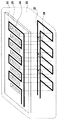
図1のトランスのコイルパターンの具体例を図3の模式図に示す。図3では、一次巻き線の8本の導体が全て直列接続されていて、巻き数としては4回である状態を示している。ただし、並列接続を組み合わせることにより種々の巻き数を構成することは可能である。所定形状に加工されたリードフレーム状の一次導体12の対向する位置に、同様な形状に加工されたリードフレーム状の二次巻き線を構成する二次導体13が配置される。ただし、分かりやすく描画する便宜上、図3では一次導体12と二次導体13とがかなり離れて図示されているが、図1に断面図で示すように、実際にはより接近して、一定距離の間隔で配線されているものとする。
【0038】
並列接続の場合には、図3の下方に示すように、二次導体13が交差する部分(ジャンパ部17)が出てくる。
【0039】
一次導体12および二次導体13の周囲空間に、フェライトにより絶縁被覆された金属粒子からなる磁性圧粉体11が密に充填されてコイル内蔵圧粉コア10が形成され、このコイル内蔵圧粉コア10により閉磁路を構成している。
【0040】
次に、図1、図3に示すコイル内蔵圧粉コア10である、電源用トランスの製造方法の具体例について説明する。
【0041】
0.5mm厚さのCu板を準備し、この板を図3の一次導線12の形状にプレスにより打ち抜くことでリードフレームを作製する。同様に、Cu板を二次導線13の形状に打ち抜くことでリードフレームを作製する。並列接続の場合、二次導体13が交差する部分が出てくる。この場合、並列の1ターン、1ターン毎に個別に打ち抜き、交差する部分については、打抜き時にプレスの金型で凸加工を行うことでジャンパ部17を作製する。こうして、個別に打ち抜いたリードフレーム状の導線をまとめて二次導線13とする。
【0042】
リードフレーム状の一次導線12と二次導線13の面に低融点ガラスペーストをディッピングにより塗工する。その後、これらを500℃で焼き付けることで、リードフレーム導体をガラス膜でコーティングする。
【0043】
本実施形態では、ガラス膜のコーティングをディッピングにより行ったが、はけ塗りでもかまわない。または、焼付けでなく、溶射、スパッタ、CVD(化学気相堆積)、ジェットプリンティングなどにより、リードフレーム導体上にガラス膜を直接形成で行ってもかまわない。さらに、ガラス膜でなくても、酸化物絶縁材料であればよく、アルミナ、ムライト、ジルコニアまたはその化合物でもかまわない。
【0044】
箱型の超鋼製の金型(図示しない)中に、フェライトにより絶縁被覆された金属粒子からなる磁性粉末を必要量だけ投入し、磁性粉末全体をよくならして平らにした後、磁性粉末上に上記のように作製したガラス膜付きのリードフレーム二次導体13を設置する。その上からその同じ磁性粉末を必要量だけ投入し、磁性粉末全体をよくならして平らにする。さらに、同じ手順で、磁性粉末上にガラス膜付きのリードフレームー次導体12を設置し、磁性粉末を投入し、磁性粉末全体をよくならして平らにする。最後に、上パンチ(型押し板:図示しない)をはめ込み、プレスにより1〜10ton/cm2で圧縮成形する。
【0045】
このようにして、フェライトにより絶縁被覆された金属粒子からなる磁性粉末1中に、酸化物絶縁材料をコーティングしたリードフレーム形状の一次導体12と二次導体13とが埋め込まれたコイル内蔵圧粉コア10である、電源用トランスを作製した。
【0046】
次に、図1を参照して、上記のようにして作製した薄型の電源用トランスの動作を説明する。
【0047】
図1の断面において一対の導体について見ると、互いに対向した位置に一次側導体12と二次側導体13とが置かれ、両導体を囲んだ磁性圧粉体(フェライトコア)11により閉磁路を構成している。すなわち、隣接する導体12、13は図3に示すように互いに逆向きの接続であるので、両導体12、13に流れる電流が作る磁束は、図1に矢印で示すように、一区画の閉磁路のみを通ることになる。これにより、一次側導体12に印加され電圧はそのまま二次側導体13に現われ、この区画では変圧比1:1のトランスを構成する。
【0048】
図3に示すように、一次側導体12は全て直列接続、二次側導体13は全て並列接続とすると、その構成では、変圧比4:1のトランスが構成されることになる。
【0049】
電源用トランスのコイル構成は、パターン巻き数とパターン幅、奥行き長さによって決まる。例えば、50Wクラスのスイッチング電源用途としては、奥行き50mm,24巻きのミヤンダ巻き(図3のようなジクザク形状)のコイルを用いる。ただし、このパターン形状は一般的なもので、本発明を限定するものではない。
【0050】
コイルを形成する導体12、13として、本実施形態では銅を用いていているが、例えば、金、銀、アルミニウムなどの単金属、あるいはそれらを基とする合金などの導電率が高い金属材料を採用することも、勿論可能である。
【0051】
本実施形態のトランスでは、一次のコイル(12)と二次のコイル(13)間、および、コイルとコア(11)の間において、試験電圧1kVでの絶縁性を確保することができた。また、10MHzの高周波領域においても渦電流損失はほとんど無く、透磁率100、飽和磁化強度1.4テスラを得ることができた。
【0052】
本実施形態ではトランスの例を示したが、二次巻き線を省略し、一次巻き線のみを用いて、上記と同様の構成でリアクトルを構成できる。
【0053】
(第2の実施形態)
本発明の第2の実施形態では、本発明の第1の実施形態で例示した上述のリードフレーム状のコイル(巻き線)に対して、コイルパターンを絶縁基板上に形成した場合の構造例を示す。
【0054】
図4は本発明の第2の実施形態におけるトランスの構成例を示す模式図である。図4において、絶縁基板25には、一定ピッチで磁性材料が入り込むための貫通孔26が複数個配設されている。そして、絶縁基板25の片面には、一次巻き線を構成する一次導体22のパターンが複数の貫通孔26の間に塗工、焼き付けされている。図4では一次巻き線の8本の導体が全て直列接続されていて、巻き数としては4回である状態を示しているが、並列接続を組み合わせることにより種々の巻き数を構成することが可能である。
【0055】
また、絶縁基板25の反対側の面内には、二次巻き線を構成する二次導体23のパターンが、やはり上記複数の貫通孔26の間に塗工、焼き付けされている。図4では、裏面側も同時に描画する都合上、二次導体23のパターンが絶縁基板25から離れて図示されているが、実際には、一次導体22のパターンと同じく絶縁基板25の反対側の面上に配線されているものとする。並列接続の場合は、二次導体23のパターンが交差する部分(28)が出てくる。一次導体22のパターンおよび二次導体23のパターンを取り囲んで、フェライトにより絶縁被覆された金属粒子からなる磁性粉末21が圧粉されてコイル内蔵圧粉コアが形成され、このコイル内蔵圧粉コアにより閉磁路を構成している。
【0056】
次に、本実施形態のトランスの製造方法の具体例について説明する。
長穴形状の貫通穴26を形成した0,635mm厚さのアルミナ製の絶縁基板25を準備し、その基板25の両面にスクリーン印刷により銀粉末と有機成分からなる導電性ぺーストを図4の22、23で示すようなパターンに塗工する。その後、600〜900℃の還元雰囲気で導電性ぺーストをアルミナ絶縁基板25上に焼き付ける。こうすることで、絶縁基板25の両面に0.1mm厚さの銀からなる導体22,23のパターンが形成される。本実施形態では、導体22,23のパターンの形成にスクリーン印刷を用いているが、ジェットプリンティングでもかまわない。
【0057】
並列接続の場合は、導体パターンが交差する部分が出てくる。この場合は、交差する部分の絶縁基板面に対して下側の導体パターンを形成した後、交差する部分とその周辺にガラスペーストなどの酸化物絶縁材料をコーティングすることで絶縁膜28を形成し、その後で絶縁基板面に対して上側となる導体パターンを形成する。本実施形態では交差する部分に絶縁膜28を用いているが、これに代えて、導体をスルーホールによって一度一次導体側の面に引き出し、再度スルーホールにより二次導体側に戻る形の接続法でも良い。
【0058】
次に、導体22,23のパターンを覆うように、スクリーン印刷により低融点ガラスペーストを絶縁基板25の両面に塗工する。その後、絶縁基板25を500℃で焼き付けることで、導体22,23のパターンをガラス膜(図示しない)でコーティングする。
【0059】
本実施形態では、ガラス膜のコーティングをスクリーン印刷法により行ったが、ディッピングや、はけ塗りでもかまわない。また、本実施形態では塗工と焼付けを採用したが、これに代えて、溶射、スパッタ、CVD、ジェットプリンティングなどにより、直接形成でガラス膜を生成してもかまわない。さらに、ガラス膜でなくても、酸化物絶縁材料であればよく、アルミナ、ムライト、ジルコニアまたはその化合物でもかまわない。
【0060】
次に、箱型の超鋼製の金型(図示しない)中に、フェライトにより絶縁被覆された金属粒子からなる磁性粉末21を所定量だけ投入し、その磁性粉末を全体によくならして平らにした後、その磁性粉末の上に上記のように作製したガラス膜コーティング付きの回路基板25を設置する。さらに、その回路基板25の上から上記と同じ磁性粉末21を投入し、その磁性粉末を全体によくならして平らにする。そして、金型内の磁性粉末上に上パンチ(図示しない)をはめ込み、プレスにより1〜10ton/cm2で圧縮成形する。
【0061】
このようにして、絶縁基板25上にパターニングされて酸化物絶縁材料でコーティングされたコイルが、フェライトにより絶縁被覆された金属粒子からなる磁性粉末21中に内蔵された状態のコイル内蔵圧粉コアである電源用トランスが作製される。
【0062】
本実施形態のトランスでは、一次のコイルと二次のコイル間、および、コイルとコア間において、試験電圧1kVでの絶縁性を確保することができた。10MHzの高周波領域においても渦電流損失はほとんど無く、透磁率100、飽和磁化強度1.4テスラを得ることができた。
【0063】
本実施形態ではトランスの例を示したが、二次巻き線を省略し、一次巻き線のみを用いて、上記と同様の構成でリアクトルを構成できる。
【0064】
(第3の実施形態)
上述の第1、第2の実施形態ではコアの圧縮成形を通常のプレスで行っているのに対して、本発明の第3の実施形態では、その圧縮成形をホットプレス成形で行う。即ち、超鋼製の金型中に、フェライトにより絶縁被覆された金属粒子からなる磁性粉末を投入し、それを全体によくならした後、その上に上記のように作製したガラス膜コーティング付きの回路基板25を設置する。さらに、その上から上記と同じ磁性粉末を投入し、それを全体によくならす。そして、金型に上パンチをはめ込み、2ton/cm2で300℃で5分のホットプレス成形を行う。
【0065】
本実施形態のトランスでは、一次のコイルと二次のコイル間、および、コイルとコア間において、試験電圧1kVでの絶縁性を確保することができた。10MHzの高周波領域においても渦電流損失はほとんど無かった。透磁率175に向上することができ、飽和磁化強度1.4テスラを得ることができた。
【0066】
プレスにより1〜10ton/cm2で圧縮成形した状態で、200〜900℃に加熱した状態でも上記と同様の効果を得ることができた。
【0067】
本実施形態では、圧縮成形をホットプレス成形で行っているが、加熱を伴う成形によって表面拡散による磁気結合が強まればよく、そのためHIP(熱間静水圧プレス)成形、放電プラズマ焼結で圧縮成形を行っても上記と同様の効果が期待できる。
【0068】
(第4の実施形態)
本発明の第4の実施形態では、前述の本発明の第1、第2の実施形態で得られるコイル内蔵圧粉コアである電源用トランスを圧縮成形後に、300℃で5分の熱処理を行う。
【0069】
本実施形態のトランスでも、一次のコイルと二次のコイル間、および、コイルとコア間において、試験電圧1kVでの絶縁性を確保することができた。10MHzの高周波領域においても渦電流損失はほとんど無かった。透磁率150に向上することができ、飽和磁化強度1.4テスラを得ることができた。これも、表面拡散による磁気結合が強まったためと考えられる。
【0070】
(第5の実施形態)
前述の本発明の第2の実施形態では、導体22、23のパターンが形成されたガラス膜コーティング付きの回路基板25を磁性粉末21内に設置して、プレスすることでコイル内蔵圧粉コアを形成している。これに対し、本発明の第5の実施形態では、磁性粉末内に回路基板を配置する代わりに、図5の模式的な分解斜視図に示すように、金型(図示しない)等を用いて、フェライト被覆金属微粒子粉末を圧縮形成したコア材である上磁性板31と下磁性板32を用意し、この板状の上磁性板31と下磁性板32を、第2の実施形態と同様にして作製したガラス膜コーティング付きの回路基板25上に挟み込むようにしてはめ込み、コイル内蔵圧粉コアであるトランスを形成する。下磁性板32は回路基板の貫通孔26にそれぞれ勘合する複数の凸部33を有する櫛形状の板である。但し、この凸部33は下磁性板32ではなくて上磁性板31の方に設けてもかまわない。
【0071】
また特に、本実施形態では、コア材である上磁性板31と下磁性板32の表面に、絶縁性のコーティングを、アルミナの耐熱性無機接着剤の塗布で行っている。このアルミナ耐熱性無機接着剤は1液加熱硬化材として、市販されているものを用いることができる。このアルミナ塗付により、フェライト被覆金属微粒子粉末の圧縮形成体(磁性板)31、32は、高圧力の成形においてもフェライトの絶縁性能を保ちつつ、金属強磁性体微粒子同士を磁気的に結合することが可能となり、より高い透磁率と飽和磁化強度を得ることができる。
【0072】
本実施形態のトランスでは、10MHzの高周波領域においても渦電流損失はほとんど無く、透磁率70、飽和磁化強度1.0テスラを得ることができた。よって、本実施形態のコア材31、32をトランスのコア材に用いる場合、従来のフェライトとコア材と比較して、同じインダクタンス値を得るのに、体積が小さくて済み、小型化、薄型化が可能になる。
【0073】
本実施形態ではトランスの例を示したが、2次巻き線を省略して1次巻き線のみを用いて、同様の構成でリアクトルを構成できる。
【0074】
本実施形態は、薄型スイッチング電源等に用いるナノフェライト被覆磁性体の圧縮成形した時に生じる絶縁性低下の課題に対し、絶縁低下が圧縮時の金型表面でのフェライトの潰れによって起こることを見出し、その対策として上記のように絶縁性のコーティング材料で磁性体コアに表面コーティングを行い、係る課題を解決したものである。これにより、磁性体の性能をさらに向上させ、トランス、リアクトルの更なる小型化、薄型化を可能にする利点が得られる。
【0075】
(他の実施形態)
以上、本発明の実施形態を説明したが、本発明はこれに限定されない。特許請求の範囲の記載の範囲内であれば、個数やサイズ等の変更、修正、置換等は本発明の実施形態に含まれる。例えば、本発明の第1の実施形態の磁性圧粉体11を本発明の第5の実施形態で示したコア材である上磁性板31と下磁性板32とで置換えてもよい。また、本発明の第3、第4の実施形態で例示した加熱成形、熱処理を本発明の第5の実施形態に適用して好ましい。また、本発明の第5の実施形態で示した圧粉コアに対するアルミナの耐熱性無機接着剤の塗布を第1〜第4実施形態に適用しても好ましい。さらに、本発明の実施形態ではトランスとリアクトルを例示したが、本発明はこれに限らず、マイクロ電源、インバータ(INV)、サーボ、UPS(非中断電源装置)等の他の磁気部品や磁気製品にも応用可能である。
【0076】
【発明の効果】
以上説明したように、本発明によれば、絶縁性能が向上し、高周波帯域での優れた磁気特性が得られる磁気部品が実現できる。
【0077】
従って、本発明によるトランス、リアクトルは、例えば、240V入力系スイッチング電源モジュール用の主回路部分のトランス、リアクトルとして十分に使用することができる。
【0078】
また、本発明のトランス、リアクトルは、従来のスイッチング電源モジュール等に用いるトランス、リアクトルと比較して、同じインダクタンス値を得るのに、体積が小さくて済み、小型化、薄型化が可能になる。
【図面の簡単な説明】
【図1】本発明の第1の実施形態における電源用トランスの断面構造を示す断面図である。
【図2】フェライトにより絶縁被覆された金属粒子からなる磁性粉末の模式図である。
【図3】本発明の第1の実施形態における電源用トランスのコイルパターン等を示す模式図である。
【図4】本発明の第2の実施形態における電源用トランスの構成を示す模式図である。
【図5】本発明の第5の実施形態における電源用トランスの構成を示す模式的分解斜視図である。
【符号の説明】
10 コイル内蔵圧粉コア(電源用トランス、リアクトル)
11 磁性圧粉体
12 一次巻き線を構成するリードフレーム形状の一次導体
13 二次巻き線を構成するリードフレーム形状の二次導体
14 絶縁コーティング
15 金属コア
16 フェライト皮膜
17 ジャンパ部
21 フェライトにより絶縁被覆された金属粒子からなる磁性粉末
22 基板上にパターン形成された一次巻き線を構成する一次導体
23 基板上にパターン形成された二次巻き線を構成する二次導体
25 絶縁基板
26 貫通孔
28 絶縁膜(導体交差部の絶縁コーティング)
31 上磁性板(圧粉コア材)
32 下磁性板(圧粉コア材)
33 貫通孔に勘合する凸部[0001]
TECHNICAL FIELD OF THE INVENTION
The present invention relates to a dust core with a built-in coil used for an electromagnetic component and a method of manufacturing the same, and a power supply transformer and a reactor using the core and a method of manufacturing the same.
[0002]
[Prior art]
In recent years, various electronic devices have been reduced in size and weight, and low power consumption has been demanded. Accordingly, there is an increasing demand for a small switching power supply as a power supply mounted on an electronic device. In particular, switching power supplies used for small portable devices such as notebook personal computers and mobile phones, thin CRTs, and flat panel displays of televisions are strongly required to be small and thin. However, in the conventional switching power supply, magnetic components such as a transformer and a reactor, which are main components, occupy a large volume, and there is a limit in reducing the size and thickness of the switching power supply. Unless the volume of these magnetic components is reduced, it has been difficult to reduce the size and thickness of the switching power supply.
[0003]
Conventionally, magnetic cores of magnetic components such as transformers and reactors used in such switching power supplies include metal magnetic materials such as high-permeability magnetic materials such as Sendust (registered trademark) and Permalloy, and ferrites and the like. Oxide magnetic materials have been used. A metal magnetic material generally has a high saturation magnetic flux density and a high magnetic permeability, but has a low electric resistivity, so that eddy current loss increases particularly in a high frequency region. For this reason, it has not been possible to reduce the required inductance value by high-speed operation or high-frequency driving, which is the trend in recent years, to reduce the size of the magnetic component. On the other hand, an oxide magnetic material has a higher electric resistivity than a metal magnetic material, and therefore, an eddy current loss that occurs even in a high frequency region is small. However, the volume of the oxide magnetic material could not be reduced because of its low saturation magnetic flux density.
[0004]
In other words, in any of the above magnetic materials, the volume of the magnetic core is the largest factor that determines the inductance value, and the magnetic characteristics of the magnetic material itself are set to. Unless improved, it has been difficult to reduce the size and thickness of magnetic components such as transformers and reactors.
[0005]
In response to such a problem, in recent years, as a magnetic material having both advantages of a metal magnetic material and an oxide magnetic material, an insulating material having a high electric resistivity is formed on a surface of a metal magnetic material having a high saturation magnetic flux density and a high magnetic permeability. A magnetic material having a film is used. In particular, it has been proposed to form ferrite, which is an oxide magnetic material, as an insulating material of the film. For example, as in Patent Document 1, a high magnetic permeability material in which a film of a high magnetic permeability metal oxide is formed on the surface of a metal magnetic material has been proposed. Further, as in Patent Document 2, the surface of a metal magnetic material composed of particles of 1 to 10 μm is coated with a metal oxide having a spinel composition represented by M-Fex04 (M = Ni, Mn, Zn, Fe, x ≦ 2). A high-density sintered magnetic body coated with a magnetic material has been proposed.
[0006]
Furthermore, a ferromagnetic fine particle powder of a metal or an intermetallic compound whose surface is coated with a ferrite layer is compression-molded, and a magnetic path is formed between the ferroelectric particles through the ferrite layer. Has been proposed. Such a compact formed of the ferrite-coated metal fine-particle powder can magnetically couple the metal ferromagnetic fine particles while maintaining the insulating performance of the ferrite to some extent, and can suppress the eddy current. There is an advantage that high magnetic permeability and high saturation magnetization can be maintained even in the frequency domain. Therefore, when the compact of the ferrite-coated metal fine particle powder is used as a core material of a transformer, a smaller volume is required to obtain the same inductance value as compared with a conventional ferrite core material, and the transformer and the reactor are required. It can be expected that magnetic components such as the ones can be made smaller and thinner.
[0007]
Molding of a core using such insulating coated metal magnetic particles is generally performed by compression molding using a press. Then, for example, a transformer or a reactor is manufactured by winding a conductor covered with insulation around a ring-shaped core obtained by compression molding as described above. Alternatively, a transformer or a reactor is manufactured by inserting a coil in which a conductive wire is wound around an insulating bobbin in advance or a spiral coil into an EI type core (also referred to as an EI core) obtained by compression molding.
[0008]
In order to further reduce the size and thickness of a transformer or reactor having a core obtained by compression molding, a transformer or reactor having a coil built-in powder core obtained by embedding a coil made of a conductor in magnetic powder and compression molding. Has also been proposed. For example, Patent Literature 3, Patent Literature 4, and Patent Literature 5 propose such transformers or reactors.
[0009]
Patent Literature 3 proposes a method of manufacturing a magnetic core obtained by combining a magnetic powder to which an organic insulating binder is added with an electromagnetic coil and compressing and molding the same in the same mold to obtain a dust core. ing.
[0010]
Patent Literature 4 proposes an inductor having a high induction coefficient, in which a coil is compression-molded in a state where the coil is sandwiched between powder compacts from above and below to obtain an inductor in which the coil is sealed in a magnetic body.
[0011]
Patent Literature 5 proposes a coil-enclosed type dust core having a small variation in the position of a built-in coil by a two-stage compression process.
[0012]
[Patent Document 1]
JP-A-53-91397
[0013]
[Patent Document 2]
JP-A-56-38402
[0014]
[Patent Document 3]
JP-B-54-28577
[0015]
[Patent Document 4]
Patent No. 3108931
[0016]
[Patent Document 5]
JP 2001-267160 A
[0017]
[Problems to be solved by the invention]
The compression-molded body obtained by compressing the insulating-coated metal fine particle powder as described in Patent Documents 4 and 5 described above ensures insulation between the coil and the core by insulating coating of individual magnetic metal particles. As a result, in the case of a low voltage, the insulation between the coil and the core, or in the case of using as a transformer, the insulation between the primary coil and the secondary coil is ensured by the insulation of the insulating coating of each magnetic metal particle. It is possible.
[0018]
However, when the voltage applied to the coil is high, particularly when used as a power transformer, the insulating coating between the individual magnetic metal particles described above does not provide sufficient insulation between the coil and the core. The potential of the core changes. In addition, when used as a transformer, the edge between the primary coil and the secondary coil cannot be secured through the core.
[0019]
Therefore, if the insulating coating of each magnetic metal particle is made thick to ensure insulation, magnetic coupling between the magnetic particles is hindered, and magnetic characteristics such as magnetic permeability characteristics deteriorate. As described above, the thickness of the insulating film only needs to provide insulation between the particles, and when the film becomes thicker, the magnetic permeability, the saturation magnetic flux density, etc., decrease, and it is important to form a stable thin film uniformly. .
[0020]
On the other hand, in the manufacturing method described in Patent Document 3, when the molding pressure is increased, the resin layer coating the coil is deformed. In particular, due to the bias of the molding pressure distribution, not only cracks but also the film pressure of the resin layer becomes extremely thin at a corner where a substantially large pressure is applied, so that a necessary insulation distance cannot be secured.
[0021]
When the manufacturing method of the heat and pressure molding is adopted for molding the core, the deformation of the resin becomes remarkable. In the case of a core using magnetic powder consisting of metal particles that are insulated and coated with ferrite, heating causes the ferrite film portions of the particles to react with each other, resulting in necking (the baking reaction causes contact between the particles, which is originally point contact). The formation of a constricted portion called a neck (neck portion) or the formation of a neck (neck portion) significantly increases the magnetic coupling between particles. Therefore, a core having high magnetic permeability can be obtained by compression molding by molding involving heating, such as hot press molding, hot isostatic press molding, or molding by spark plasma sintering. Similar effects can be obtained by performing heat treatment after compression molding. However, if the coil is coated with a resin layer as described in Patent Literature 3, necessary insulation characteristics cannot be secured due to deterioration, deformation, carbonization, and the like of the resin layer.
[0022]
More specifically, as described above, the compression-formed body of ferrite-coated metal fine particle powder suppresses eddy currents by the insulating properties of the ferrite coating and maintains high-frequency characteristics. The compression formed body magnetically couples the metal ferromagnetic fine particles to each other by compression formation, and maintains high magnetic permeability and saturated magnetization intensity. Here, in order to obtain a higher inductance value or magnetic permeability, it is necessary to increase the pressure of the compression formation so as to bring the metal ferromagnetic fine particles as close as possible and further strengthen the magnetic coupling between the metal ferromagnetic fine particles. Deemed desirable. However, in actuality, when the pressure of the compression formation is increased, the ferrite coating may be crushed, and the metal ferromagnetic fine particles may be electrically connected to each other, causing eddy currents and degrading the frequency characteristics. There is. This decrease in insulation is more remarkable as the power supply voltage is higher.
[0023]
The conventional compression-formed body of the insulating-coated metal fine-particle powder has the above-mentioned problems. For this problem, a magnetic component such as a transformer and a reactor using the compression-formed body of the insulating-coated metal fine-particle powder as a core is used. This prevented further miniaturization.
[0024]
An object of the present invention is to solve the above-described problem of dielectric breakdown of a ferrite coating in the compression forming of a compression-formed body of ferrite-coated metal fine-particle powder, and the insulating coating suppresses eddy current and maintains high-frequency characteristics. By setting the minimum required thickness, it is possible to prevent deterioration of magnetic properties such as magnetic permeability properties, while ensuring insulation between the coil and the core at a high voltage, thereby obtaining a higher inductance value. Another object of the present invention is to provide a dust core with a built-in coil and a method for manufacturing the same, and further reduce the size and weight of power supply transformers and reactors used in various electronic devices.
[0025]
[Means for Solving the Problems]
In order to achieve the above object, a powder core with a built-in coil of the present invention used for an electromagnetic component such as a transformer for a power supply and a reactor is a metal particle in which a coil made of a conductor coated with an oxide insulating material is insulated and coated with ferrite. Embedded in a magnetic powder consisting of: and obtained by compression molding.
[0026]
Further, another form of the dust core with a built-in coil of the present invention is formed by patterning on an insulating substrate, and a coil pattern made of a conductor coated with an oxide insulating material is made of metal particles insulated and coated with ferrite. It is embedded in a magnetic powder and obtained by compression molding.
[0027]
Here, glass, alumina, silica, zirconia or a compound thereof can be adopted as the oxide insulating material coated on the conductor.
[0028]
Further, it is preferable that the surface of the coil built-in dust core is coated with an insulating material. Any of glass, alumina, silica, zirconia, or a compound thereof can be used as the insulating material. Observation of the state of dielectric breakdown of the ferrite coating in the compression forming of the compression-formed body of the ferrite-coated metal fine particle powder by SEM or the like shows that the breakdown due to the collapse of the ferrite coating is large on the surface of the molded body. This is considered to be because the ferrite-coated metal fine particles are powder before compression, and when compression molding is performed in a mold, the pressure is transmitted more directly near the mold and a higher pressure is applied. Therefore, by coating the surface of the core with an insulating coating, which often causes dielectric breakdown of the ferrite coating, it is possible to easily prevent the insulation from lowering.
[0029]
In order to achieve the above object, a power supply transformer according to the present invention is characterized in that the power supply transformer has the powder built-in core having the coil.
[0030]
In order to achieve the above object, a reactor of the present invention is characterized by having the above-mentioned dust core having a built-in coil.
[0031]
In order to achieve the above object, the manufacturing method of the present invention is a method of manufacturing the dust core with a built-in coil, wherein the compression molding includes hot press molding, hot isostatic press (HIP) molding, and spark plasma sintering. It is characterized by compression molding involving heating such as.
[0032]
Another embodiment of the production method of the present invention is characterized in that heat treatment is performed after the compression molding.
[0033]
Further, in the production method of the present invention, it is preferable that the method further includes a step of coating the surface of the dust core with a built-in coil with an insulating material.
[0034]
Further, another embodiment of the manufacturing method of the present invention is a method for manufacturing a power transformer / reactor, in which an upper magnetic plate and a lower magnetic plate as core materials are formed by compressing and forming ferrite-coated fine metal particles. A first step, a second step of coating the surfaces of the upper magnetic plate and the lower magnetic plate with an insulating material, and a conductor formed by patterning on an insulating substrate and coated with an oxide insulating material A step of forming a coil pattern consisting of: and mounting the upper magnetic plate that has been subjected to the second step on the upper surface of the insulating substrate obtained in the third step; And a fourth step of mounting the lower magnetic plate after the second step.
[0035]
BEST MODE FOR CARRYING OUT THE INVENTION
Hereinafter, embodiments of the present invention will be described in detail with reference to the drawings.
(1st Embodiment)
FIG. 1 is a cross-sectional view illustrating a configuration example of a transformer according to the first embodiment of the present invention. As shown in FIG. 1, a
[0036]
This magnetic powder has a structure as shown in FIG. The individual particles of the magnetic powder are obtained by forming a
[0037]
A specific example of the coil pattern of the transformer of FIG. 1 is shown in the schematic diagram of FIG. FIG. 3 shows a state in which all eight conductors of the primary winding are connected in series, and the number of turns is four. However, it is possible to configure various numbers of turns by combining parallel connections. A
[0038]
In the case of the parallel connection, as shown in the lower part of FIG. 3, a portion (jumper portion 17) where the
[0039]
The space around the
[0040]
Next, a specific example of a method for manufacturing a power transformer, which is the
[0041]
A 0.5 mm-thick Cu plate is prepared, and the plate is punched out into a shape of the
[0042]
A low-melting glass paste is applied to the surfaces of the lead frame-shaped
[0043]
In the present embodiment, the coating of the glass film is performed by dipping, but brush coating may be performed. Alternatively, instead of baking, a glass film may be directly formed on the lead frame conductor by thermal spraying, sputtering, CVD (chemical vapor deposition), jet printing, or the like. Further, the material is not limited to a glass film, but may be any oxide insulating material, and may be alumina, mullite, zirconia, or a compound thereof.
[0044]
A necessary amount of magnetic powder consisting of metal particles coated with ferrite is coated in a box-shaped super steel mold (not shown), and the entire magnetic powder is smoothed and flattened. The lead frame
[0045]
In this way, the coil-embedded dust core in which the
[0046]
Next, the operation of the thin power transformer manufactured as described above will be described with reference to FIG.
[0047]
Looking at the pair of conductors in the cross section of FIG. 1, a
[0048]
As shown in FIG. 3, if all the primary-
[0049]
The coil configuration of the power transformer is determined by the number of pattern turns, the pattern width, and the depth length. For example, for a 50 W class switching power supply, a coil of 50 windings with a depth of 50 mm and 24 turns in a zigzag shape as shown in FIG. 3 is used. However, this pattern shape is general and does not limit the present invention.
[0050]
Although copper is used in the present embodiment as the
[0051]
In the transformer according to the present embodiment, insulation between the primary coil (12) and the secondary coil (13) and between the coil and the core (11) at a test voltage of 1 kV could be secured. Even in the high frequency region of 10 MHz, there was almost no eddy current loss, and a magnetic permeability of 100 and a saturation magnetization of 1.4 Tesla could be obtained.
[0052]
In the present embodiment, the example of the transformer is shown. However, the secondary winding is omitted, and the reactor can be configured in the same configuration as described above using only the primary winding.
[0053]
(Second embodiment)
In the second embodiment of the present invention, a structural example in which a coil pattern is formed on an insulating substrate with respect to the above-described lead frame-shaped coil (winding) exemplified in the first embodiment of the present invention. Show.
[0054]
FIG. 4 is a schematic diagram illustrating a configuration example of a transformer according to the second embodiment of the present invention. In FIG. 4, a plurality of through
[0055]
A pattern of the
[0056]
Next, a specific example of the method for manufacturing a transformer according to the present embodiment will be described.
An
[0057]
In the case of parallel connection, a portion where the conductor patterns intersect appears. In this case, an insulating
[0058]
Next, a low-melting glass paste is applied to both surfaces of the insulating
[0059]
In the present embodiment, the coating of the glass film is performed by the screen printing method, but may be dipping or brushing. In the present embodiment, coating and baking are adopted. Alternatively, a glass film may be formed directly by thermal spraying, sputtering, CVD, jet printing, or the like. Further, the material is not limited to a glass film, but may be any oxide insulating material, and may be alumina, mullite, zirconia, or a compound thereof.
[0060]
Next, a predetermined amount of the
[0061]
In this way, the coil-coated dust core in a state where the coil patterned on the insulating
[0062]
In the transformer according to the present embodiment, insulation between the primary coil and the secondary coil and between the coil and the core at a test voltage of 1 kV could be secured. Even in the high frequency region of 10 MHz, there was almost no eddy current loss, and a magnetic permeability of 100 and a saturation magnetization of 1.4 Tesla could be obtained.
[0063]
In the present embodiment, the example of the transformer is shown. However, the secondary winding is omitted, and the reactor can be configured in the same configuration as described above using only the primary winding.
[0064]
(Third embodiment)
In the first and second embodiments described above, the compression molding of the core is performed by a normal press, whereas in the third embodiment of the present invention, the compression molding is performed by hot press molding. That is, in a super-steel mold, a magnetic powder composed of metal particles insulated and coated with ferrite is charged, and after it is improved as a whole, the glass powder coated with the glass film prepared as described above is provided thereon. The
[0065]
In the transformer according to the present embodiment, insulation between the primary coil and the secondary coil and between the coil and the core at a test voltage of 1 kV could be secured. There was almost no eddy current loss even in the high frequency region of 10 MHz. The magnetic permeability was improved to 175, and a saturation magnetization intensity of 1.4 Tesla was obtained.
[0066]
1 to 10 ton / cm by press 2 The same effect as above could be obtained in the state where the composition was heated at 200 to 900 ° C. in the state where it was compression molded.
[0067]
In the present embodiment, the compression molding is performed by hot press molding, but it is sufficient that the magnetic coupling due to surface diffusion is strengthened by molding accompanied by heating. Therefore, compression is performed by HIP (hot isostatic press) molding and discharge plasma sintering. Even if molding is performed, the same effect as above can be expected.
[0068]
(Fourth embodiment)
In the fourth embodiment of the present invention, a heat treatment is performed at 300 ° C. for 5 minutes after compression molding of the power transformer, which is the dust core with a built-in coil, obtained in the first and second embodiments of the present invention. .
[0069]
Also in the transformer of the present embodiment, insulation between the primary coil and the secondary coil and between the coil and the core at a test voltage of 1 kV could be secured. There was almost no eddy current loss even in the high frequency region of 10 MHz. The permeability was improved to 150, and a saturation magnetization intensity of 1.4 Tesla was obtained. This is probably because magnetic coupling due to surface diffusion was strengthened.
[0070]
(Fifth embodiment)
In the above-described second embodiment of the present invention, the
[0071]
In particular, in the present embodiment, the surface of the upper
[0072]
In the transformer of this embodiment, eddy current loss was hardly found even in a high frequency region of 10 MHz, and a permeability of 70 and a saturation magnetization of 1.0 Tesla could be obtained. Therefore, when the
[0073]
In the present embodiment, an example of a transformer has been described, but a reactor can be configured with a similar configuration using only the primary winding without the secondary winding.
[0074]
The present embodiment has found that, with respect to the problem of insulation deterioration occurring when compression molding of a nano-ferrite coated magnetic material used for a thin switching power supply or the like, insulation deterioration is caused by crushing of ferrite on a mold surface during compression, As a countermeasure, the magnetic core is surface-coated with an insulating coating material as described above to solve the above-mentioned problem. Thereby, there is obtained an advantage that the performance of the magnetic body is further improved, and the transformer and the reactor can be further reduced in size and thickness.
[0075]
(Other embodiments)
Although the embodiment of the present invention has been described above, the present invention is not limited to this. Within the scope of the claims, changes, corrections, replacements, and the like of the number and size are included in the embodiments of the present invention. For example, the magnetic
[0076]
【The invention's effect】
As described above, according to the present invention, it is possible to realize a magnetic component having improved insulation performance and excellent magnetic properties in a high frequency band.
[0077]
Therefore, the transformer and the reactor according to the present invention can be sufficiently used as, for example, a transformer and a reactor of a main circuit portion for a 240 V input system switching power supply module.
[0078]
Further, the transformer and the reactor according to the present invention require a smaller volume for obtaining the same inductance value as compared with a transformer and a reactor used in a conventional switching power supply module and the like, and can be reduced in size and thickness.
[Brief description of the drawings]
FIG. 1 is a cross-sectional view showing a cross-sectional structure of a power transformer according to a first embodiment of the present invention.
FIG. 2 is a schematic diagram of a magnetic powder composed of metal particles insulated and coated with ferrite.
FIG. 3 is a schematic diagram showing a coil pattern and the like of a power transformer according to the first embodiment of the present invention.
FIG. 4 is a schematic diagram illustrating a configuration of a power transformer according to a second embodiment of the present invention.
FIG. 5 is a schematic exploded perspective view illustrating a configuration of a power transformer according to a fifth embodiment of the present invention.
[Explanation of symbols]
10 Dust core with built-in coil (power supply transformer, reactor)
11 Magnetic compact
12. Lead frame-shaped primary conductor constituting primary winding
13. Lead frame-shaped secondary conductor that constitutes the secondary winding
14 Insulation coating
15 Metal core
16 Ferrite film
17 Jumper
21 Magnetic powder consisting of metal particles insulated with ferrite
22 Primary conductor constituting primary winding patterned on substrate
23 Secondary conductor forming a secondary winding patterned on a substrate
25 Insulating substrate
26 Through hole
28 Insulation film (insulation coating at the intersection of conductors)
31 Upper magnetic plate (dust core material)
32 lower magnetic plate (dust core material)
33 Convex part to fit into through hole
Claims (14)
酸化物絶縁材料をコーティングした導体からなるコイルが、フェライトにより絶縁被覆された金属粒子からなる磁性粉末中に埋め込まれ、圧縮成形して得られたことを特徴とするコイル内蔵圧粉コア。It is a dust core with a built-in coil used for electromagnetic parts such as power transformers and reactors,
A dust core with a built-in coil obtained by embedding a coil made of a conductor coated with an oxide insulating material in a magnetic powder made of metal particles coated with ferrite and compressing and molding it.
絶縁基板上にパターニングして形成され、酸化物絶縁材料をコーティングした導体からなるコイルパターンが、フェライトにより絶縁被覆された金属粒子からなる磁性粉末中に埋め込まれ、圧縮成形して得られたことを特徴とするコイル内蔵圧粉コア。It is a dust core with a built-in coil used for electromagnetic parts such as power transformers and reactors,
A coil pattern made of a conductor formed by patterning on an insulating substrate and coated with an oxide insulating material is embedded in a magnetic powder made of metal particles insulated and coated with ferrite, and is obtained by compression molding. Dust core with built-in coil.
酸化物絶縁材料によりコーティングされた導体からなるコイルを、フェライトにより絶縁被覆された金属粒子からなる磁性粉末中に埋め込む第1の工程と、
前記第1の工程により前記コイルが前記磁性粉末中に埋め込まれたものを圧縮成形して内蔵圧粉コアを得る第2の工程と
を有することを特徴とするコイル内蔵圧粉コアの製造方法。A method for producing a coil built-in dust core used for an electromagnetic component such as a power transformer and a reactor,
A first step of embedding a coil made of a conductor coated with an oxide insulating material in a magnetic powder made of metal particles insulated and coated with ferrite;
A step of compression-molding the coil in which the coil is embedded in the magnetic powder in the first step to obtain a built-in dust core.
絶縁基板上にパターニングして形成され、酸化物絶縁材料によりコーティングされた導体からなるコイルパターンを、フェライトにより絶縁被覆された金属粒子からなる磁性粉末中に埋め込第1の工程と、
前記第1の工程により前記コイルパターンが前記磁性粉末中に埋め込まれたものを圧縮成形して内蔵圧粉コアを得る第2の工程と
を有することを特徴とするコイル内蔵圧粉コアの製造方法。A method for producing a coil built-in dust core used for an electromagnetic component such as a power transformer and a reactor,
A first step of embedding a coil pattern made of a conductor formed by patterning on an insulating substrate and coated with an oxide insulating material in a magnetic powder made of metal particles insulated and coated with ferrite;
A step of compression-molding the magnetic powder in which the coil pattern is embedded in the magnetic powder in the first step to obtain a built-in dust core. .
前記上磁性板と前記下磁性板の表面に絶縁性材料でコーティングを施す第2の工程と、
絶縁基板上にパターニングして形成され、酸化物絶縁材料によりコーティングされた導体からなるコイルパターンを形成する第3の工程と、
前記第3の工程で得られた前記絶縁基板上の上面に前記第2の工程を経た前記上磁性板を装着し、同絶縁基板上の下面に前記第2の工程を経た前記下磁性板を装着する第4の工程と
を有することを特徴とする電源用トランスの製造方法。A first step of forming an upper magnetic plate and a lower magnetic plate as core materials by compressing and forming ferrite-coated metal fine particle powder;
A second step of coating a surface of the upper magnetic plate and the lower magnetic plate with an insulating material;
A third step of forming a coil pattern made of a conductor formed by patterning on an insulating substrate and coated with an oxide insulating material;
The upper magnetic plate passed through the second step is mounted on the upper surface of the insulating substrate obtained in the third step, and the lower magnetic plate passed through the second step is placed on the lower surface of the insulating substrate. And a fourth step of mounting the transformer.
前記上磁性板と前記下磁性板の表面に絶縁性材料でコーティングを施す第2の工程と、
絶縁基板上にパターニングして形成され、酸化物絶縁材料によりコーティングされた導体からなるコイルパターンを形成する第3の工程と、
前記第3の工程で得られた前記絶縁基板上の上面に前記第2の工程を経た前記上磁性板を装着し、同絶縁基板上の下面に前記第2の工程を経た前記下磁性板を装着する第4の工程と
を有することを特徴とするリアクトルの製造方法。A first step of forming an upper magnetic plate and a lower magnetic plate as core materials by compressing and forming ferrite-coated metal fine particle powder;
A second step of coating a surface of the upper magnetic plate and the lower magnetic plate with an insulating material;
A third step of forming a coil pattern made of a conductor formed by patterning on an insulating substrate and coated with an oxide insulating material;
The upper magnetic plate passed through the second step is mounted on the upper surface of the insulating substrate obtained in the third step, and the lower magnetic plate passed through the second step is placed on the lower surface of the insulating substrate. And a fourth step of mounting the reactor.
Priority Applications (1)
| Application Number | Priority Date | Filing Date | Title |
|---|---|---|---|
| JP2003139599A JP2004342943A (en) | 2003-05-16 | 2003-05-16 | Compressed powder core incorporating coils, its manufacturing method, transformer and reactor for power sources using the core, and their manufacturing method |
Applications Claiming Priority (1)
| Application Number | Priority Date | Filing Date | Title |
|---|---|---|---|
| JP2003139599A JP2004342943A (en) | 2003-05-16 | 2003-05-16 | Compressed powder core incorporating coils, its manufacturing method, transformer and reactor for power sources using the core, and their manufacturing method |
Publications (1)
| Publication Number | Publication Date |
|---|---|
| JP2004342943A true JP2004342943A (en) | 2004-12-02 |
Family
ID=33528626
Family Applications (1)
| Application Number | Title | Priority Date | Filing Date |
|---|---|---|---|
| JP2003139599A Pending JP2004342943A (en) | 2003-05-16 | 2003-05-16 | Compressed powder core incorporating coils, its manufacturing method, transformer and reactor for power sources using the core, and their manufacturing method |
Country Status (1)
| Country | Link |
|---|---|
| JP (1) | JP2004342943A (en) |
Cited By (5)
| Publication number | Priority date | Publication date | Assignee | Title |
|---|---|---|---|---|
| JP2006186072A (en) * | 2004-12-27 | 2006-07-13 | Fuji Electric Holdings Co Ltd | Manufacturing method of compound magnetic component |
| JP2009511868A (en) * | 2005-10-07 | 2009-03-19 | ビランコ | Current and magnetic field sensor, control method for the sensor, and magnetic core for the sensor |
| JP2013153165A (en) * | 2013-01-22 | 2013-08-08 | Vacuumschmelze Gmbh & Co Kg | Complex structure having magnetocalorically active material and production method thereof |
| US9666340B2 (en) | 2007-12-27 | 2017-05-30 | Vacuumschmelze Gmbh & Co. Kg | Composite article with magnetocalorically active material and method for its production |
| CN114551075A (en) * | 2022-01-05 | 2022-05-27 | 深圳市信维通信股份有限公司 | Inductor manufacturing method |
-
2003
- 2003-05-16 JP JP2003139599A patent/JP2004342943A/en active Pending
Cited By (7)
| Publication number | Priority date | Publication date | Assignee | Title |
|---|---|---|---|---|
| JP2006186072A (en) * | 2004-12-27 | 2006-07-13 | Fuji Electric Holdings Co Ltd | Manufacturing method of compound magnetic component |
| JP2009511868A (en) * | 2005-10-07 | 2009-03-19 | ビランコ | Current and magnetic field sensor, control method for the sensor, and magnetic core for the sensor |
| KR101253581B1 (en) * | 2005-10-07 | 2013-04-11 | 닐로지 | Current and magnetic field sensors, control method and magnetic core for said sensors |
| US8803520B2 (en) | 2005-10-07 | 2014-08-12 | Neelogy | Magnetic core with superparamagnetic particles for current and magnetic field sensors |
| US9666340B2 (en) | 2007-12-27 | 2017-05-30 | Vacuumschmelze Gmbh & Co. Kg | Composite article with magnetocalorically active material and method for its production |
| JP2013153165A (en) * | 2013-01-22 | 2013-08-08 | Vacuumschmelze Gmbh & Co Kg | Complex structure having magnetocalorically active material and production method thereof |
| CN114551075A (en) * | 2022-01-05 | 2022-05-27 | 深圳市信维通信股份有限公司 | Inductor manufacturing method |
Similar Documents
| Publication | Publication Date | Title |
|---|---|---|
| Djuric et al. | Design, modeling, and analysis of a compact planar transformer | |
| JP4049246B2 (en) | Coil-enclosed magnetic component and method for manufacturing the same | |
| JP4971432B2 (en) | Inductive element and method for manufacturing the inductive element | |
| US20150102888A1 (en) | Multilayer electronic component | |
| US20130038417A1 (en) | Coil component and manufacturing method thereof | |
| JP2004311944A (en) | Chip power inductor | |
| KR101659248B1 (en) | Inductor and manufacturing method thereof | |
| JPH09129435A (en) | Coupled magnetic core | |
| JP4043306B2 (en) | Planar magnetic element | |
| JP2008288370A (en) | Surface mounting inductor, and manufacturing method thereof | |
| JP2006165212A (en) | Inductance element and its manufacturing process, and wiring board | |
| TW201903790A (en) | Inductance element and electronic and electrical device | |
| JP2005317679A (en) | Magnetic device and its manufacturing method | |
| JPH11144971A (en) | Coil parts and power supply using the same | |
| JP2004014837A (en) | Plane magnetic element | |
| WO2018235550A1 (en) | Coil component | |
| JPH11273980A (en) | Method for manufacturing inductor | |
| JP2004342943A (en) | Compressed powder core incorporating coils, its manufacturing method, transformer and reactor for power sources using the core, and their manufacturing method | |
| CN111489890B (en) | Manufacturing method of patch power inductor | |
| JP2003257744A (en) | Magnetic element, manufacturing method thereof, and power-supply module using the same | |
| US9041506B2 (en) | Multilayer inductor and method of manufacturing the same | |
| JP2008147324A (en) | Inductance element | |
| JP2005260073A (en) | Inductance element and its manufacturing method | |
| KR101310360B1 (en) | Winding-type chip inductor for power and manufacturing method thereof | |
| JP3162692B2 (en) | Inductors and transformers |
Legal Events
| Date | Code | Title | Description |
|---|---|---|---|
| A621 | Written request for application examination |
Free format text: JAPANESE INTERMEDIATE CODE: A621 Effective date: 20050614 |
|
| A711 | Notification of change in applicant |
Free format text: JAPANESE INTERMEDIATE CODE: A711 Effective date: 20070726 |
|
| A521 | Written amendment |
Free format text: JAPANESE INTERMEDIATE CODE: A821 Effective date: 20070913 |
|
| RD02 | Notification of acceptance of power of attorney |
Free format text: JAPANESE INTERMEDIATE CODE: A7422 Effective date: 20070913 |
|
| A131 | Notification of reasons for refusal |
Effective date: 20071127 Free format text: JAPANESE INTERMEDIATE CODE: A131 |
|
| A02 | Decision of refusal |
Free format text: JAPANESE INTERMEDIATE CODE: A02 Effective date: 20080404 |