JP2004342632A - Method of manufacturing semiconductor device - Google Patents
Method of manufacturing semiconductor device Download PDFInfo
- Publication number
- JP2004342632A JP2004342632A JP2003133837A JP2003133837A JP2004342632A JP 2004342632 A JP2004342632 A JP 2004342632A JP 2003133837 A JP2003133837 A JP 2003133837A JP 2003133837 A JP2003133837 A JP 2003133837A JP 2004342632 A JP2004342632 A JP 2004342632A
- Authority
- JP
- Japan
- Prior art keywords
- insulating film
- metal
- etching
- metal wiring
- copper
- Prior art date
- Legal status (The legal status is an assumption and is not a legal conclusion. Google has not performed a legal analysis and makes no representation as to the accuracy of the status listed.)
- Pending
Links
Images


Classifications
-
- H—ELECTRICITY
- H01—ELECTRIC ELEMENTS
- H01L—SEMICONDUCTOR DEVICES NOT COVERED BY CLASS H10
- H01L22/00—Testing or measuring during manufacture or treatment; Reliability measurements, i.e. testing of parts without further processing to modify the parts as such; Structural arrangements therefor
- H01L22/20—Sequence of activities consisting of a plurality of measurements, corrections, marking or sorting steps
-
- H—ELECTRICITY
- H01—ELECTRIC ELEMENTS
- H01L—SEMICONDUCTOR DEVICES NOT COVERED BY CLASS H10
- H01L21/00—Processes or apparatus adapted for the manufacture or treatment of semiconductor or solid state devices or of parts thereof
- H01L21/70—Manufacture or treatment of devices consisting of a plurality of solid state components formed in or on a common substrate or of parts thereof; Manufacture of integrated circuit devices or of parts thereof
- H01L21/71—Manufacture of specific parts of devices defined in group H01L21/70
- H01L21/768—Applying interconnections to be used for carrying current between separate components within a device comprising conductors and dielectrics
- H01L21/76801—Applying interconnections to be used for carrying current between separate components within a device comprising conductors and dielectrics characterised by the formation and the after-treatment of the dielectrics, e.g. smoothing
- H01L21/76802—Applying interconnections to be used for carrying current between separate components within a device comprising conductors and dielectrics characterised by the formation and the after-treatment of the dielectrics, e.g. smoothing by forming openings in dielectrics
- H01L21/76805—Applying interconnections to be used for carrying current between separate components within a device comprising conductors and dielectrics characterised by the formation and the after-treatment of the dielectrics, e.g. smoothing by forming openings in dielectrics the opening being a via or contact hole penetrating the underlying conductor
-
- H—ELECTRICITY
- H01—ELECTRIC ELEMENTS
- H01L—SEMICONDUCTOR DEVICES NOT COVERED BY CLASS H10
- H01L21/00—Processes or apparatus adapted for the manufacture or treatment of semiconductor or solid state devices or of parts thereof
- H01L21/70—Manufacture or treatment of devices consisting of a plurality of solid state components formed in or on a common substrate or of parts thereof; Manufacture of integrated circuit devices or of parts thereof
- H01L21/71—Manufacture of specific parts of devices defined in group H01L21/70
- H01L21/768—Applying interconnections to be used for carrying current between separate components within a device comprising conductors and dielectrics
- H01L21/76801—Applying interconnections to be used for carrying current between separate components within a device comprising conductors and dielectrics characterised by the formation and the after-treatment of the dielectrics, e.g. smoothing
- H01L21/76802—Applying interconnections to be used for carrying current between separate components within a device comprising conductors and dielectrics characterised by the formation and the after-treatment of the dielectrics, e.g. smoothing by forming openings in dielectrics
- H01L21/76814—Applying interconnections to be used for carrying current between separate components within a device comprising conductors and dielectrics characterised by the formation and the after-treatment of the dielectrics, e.g. smoothing by forming openings in dielectrics post-treatment or after-treatment, e.g. cleaning or removal of oxides on underlying conductors
-
- H—ELECTRICITY
- H01—ELECTRIC ELEMENTS
- H01L—SEMICONDUCTOR DEVICES NOT COVERED BY CLASS H10
- H01L21/00—Processes or apparatus adapted for the manufacture or treatment of semiconductor or solid state devices or of parts thereof
- H01L21/70—Manufacture or treatment of devices consisting of a plurality of solid state components formed in or on a common substrate or of parts thereof; Manufacture of integrated circuit devices or of parts thereof
- H01L21/71—Manufacture of specific parts of devices defined in group H01L21/70
- H01L21/768—Applying interconnections to be used for carrying current between separate components within a device comprising conductors and dielectrics
- H01L21/76838—Applying interconnections to be used for carrying current between separate components within a device comprising conductors and dielectrics characterised by the formation and the after-treatment of the conductors
-
- H—ELECTRICITY
- H01—ELECTRIC ELEMENTS
- H01L—SEMICONDUCTOR DEVICES NOT COVERED BY CLASS H10
- H01L23/00—Details of semiconductor or other solid state devices
- H01L23/52—Arrangements for conducting electric current within the device in operation from one component to another, i.e. interconnections, e.g. wires, lead frames
- H01L23/522—Arrangements for conducting electric current within the device in operation from one component to another, i.e. interconnections, e.g. wires, lead frames including external interconnections consisting of a multilayer structure of conductive and insulating layers inseparably formed on the semiconductor body
- H01L23/5226—Via connections in a multilevel interconnection structure
-
- H—ELECTRICITY
- H01—ELECTRIC ELEMENTS
- H01L—SEMICONDUCTOR DEVICES NOT COVERED BY CLASS H10
- H01L2924/00—Indexing scheme for arrangements or methods for connecting or disconnecting semiconductor or solid-state bodies as covered by H01L24/00
- H01L2924/0001—Technical content checked by a classifier
- H01L2924/0002—Not covered by any one of groups H01L24/00, H01L24/00 and H01L2224/00
-
- Y—GENERAL TAGGING OF NEW TECHNOLOGICAL DEVELOPMENTS; GENERAL TAGGING OF CROSS-SECTIONAL TECHNOLOGIES SPANNING OVER SEVERAL SECTIONS OF THE IPC; TECHNICAL SUBJECTS COVERED BY FORMER USPC CROSS-REFERENCE ART COLLECTIONS [XRACs] AND DIGESTS
- Y10—TECHNICAL SUBJECTS COVERED BY FORMER USPC
- Y10S—TECHNICAL SUBJECTS COVERED BY FORMER USPC CROSS-REFERENCE ART COLLECTIONS [XRACs] AND DIGESTS
- Y10S438/00—Semiconductor device manufacturing: process
- Y10S438/906—Cleaning of wafer as interim step
Abstract
Description
【0001】
【発明の属する技術分野】
本発明は半導体装置の製造方法、特に配線構造の製造に関するものである。
【0002】
【従来の技術】
近年の半導体集積回路は、配線材料としてアルミニウムより抵抗が低い銅が用いられるようになってきた。その加工工程ではドライエッチング技術を用いて層間絶縁膜に配線溝を形成し、その配線溝に配線材料を埋め込むダマシン法が用いられている。
【0003】
以下、図4,図5を参照して、従来の配線の製造方法を説明する。
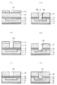
図4は半導体装置の製造における銅酸化量とコンタクト抵抗の関係を示す図である。また、図5は従来の銅配線を用いた半導体装置の製造方法を示す工程断面図であり、図5(a)は従来のヴィアホールのレジストパターン形成工程を示す工程断面図、図5(b)は従来のヴィアホール形成工程を示す工程断面図、図5(c)は従来のレジストパターンを除去する工程を示す工程断面図、図5(d)は従来の絶縁膜を開口する工程を示す工程断面図、図5(e)は従来のヴィアホール底面の洗浄工程を示す工程断面図、図5(f)は従来の金属プラグの形成工程を示す工程断面図である。
【0004】
まず、図5(a)に示すレジストパターン形成工程において、例えば、シリコンからなる半導体基板71上に、銅配線73をその周囲が酸化シリコンからなる絶縁膜72により覆われるように形成する。続いて、絶縁膜72上における銅配線73の上方に窒化シリコンからなる絶縁膜74を形成し、絶縁膜74上に酸化シリコンからなる絶縁膜75を形成した後に、開口部77を有するレジストパターン76を形成する。
【0005】
次に、図5(b)に示すヴィアホール形成工程において、プラズマドライエッチング法により、絶縁膜75に対してレジストパターン76をマスクとするエッチングを行って、ヴィアホール77aを形成する。
【0006】
次に、図5(c)に示すアッシング工程にてレジストパターン76を除去した後、図5(d)に示す金属配線露出工程において、プラズマドライエッチング法により半導体装置表面を全面エッチバックして絶縁膜74に銅配線73を露出するヴィアホール77bを形成する。この工程では、例えば、平行平板型RIE装置を用いて、エッチングガスであるCF4流量を50sccmとし、エッチング堆積物の制御ガスであるO2流量を10sccmとし、基板温度を25℃とし、RF出力を300Wとし、圧力を5Paとする。この際、エッチング反応生成物である堆積物の制御としてO2を用いているため、下地銅配線73の表面が酸化し、酸化銅層78が形成される。
【0007】
最後に、図5(e)に示すように、フッ化アンモニウムおよび酢酸アンモニウムのような有機酸を含む洗浄等に代表される酸化銅/銅のエッチング選択比がほとんど無限大の薬液で半導体装置の洗浄を行い、酸化銅層78を除去した後、図5(f)に示すようにヴィアホール77bの底面及び壁面を含めて上層配線の一部であり同じく銅からなる金属プラグ79を形成する。
【0008】
図5(d)に示すように、絶縁膜74をプラズマドライエッチング法により加工する際、エッチング装置のプラズマ発生用高周波(RF)出力やエッチング時間に依存して、下地銅配線73の表面酸化が進行し、酸化銅78が形成する。一方図5(e)の工程で用いる洗浄薬液では一応酸化銅78は除去できるのであるが、エッチング速度がたとえば0.5nm程度と小さく、工程のスループットあるいは生産性を考慮して10〜20分が処理限界である。したがって酸化銅78の形成量が大きいと、薬液でのエッチングが不十分となり、図4に示す銅酸化量と銅配線―銅プラグのコンタクト抵抗の関係から分かるように、10nmを越えて厚くなるとコンタクト抵抗のばらつきが大きくなるという問題があった。そのため絶縁膜74のドライエッチングにおいて酸化銅78の成長量およびエッチング装置の高周波出力、エッチング時間を管理、制御することが必要とされている。
【0009】
従来、銅配線の酸化量を定量化するためには、SIMS分析など製造ライン外での測定評価が必要であった。そのため製造工程中に銅酸化が過剰に進行した場合でも検知に時間がかかり、またドライエッチング条件などプロセスフィードバックが速やかにできないという問題点があった(例えば、特許文献1参照)。
【0010】
【特許文献1】
特開2001−208531号公報
【0011】
【発明が解決しようとする課題】
上記問題点を解決するために、本発明の半導体装置の製造方法は、下地銅配線の酸化銅形成量を製造ライン内で簡便に定量化することを目的とする。また、定量化した結果をエッチング装置のプロセス条件やエッチング時間制御にフィードバックしてコンタクト抵抗のばらつきを抑制することを目的とする。
【0012】
【課題を解決するための手段】
本発明の請求項1記載の半導体装置の製造方法は、半導体基板上に形成した回路に金属配線を施す工程と、前記金属配線の上に絶縁膜を形成する工程と、プラズマドライエッチング法により前記絶縁膜を選択的にエッチングして前記金属配線の表面部を露出するように前記絶縁膜にヴィアホールを形成する工程と、前記金属配線表面部と前記絶縁膜表面との第1の段差を非接触測定法で測定する工程と、前記金属膜表面部を洗浄して前記金属膜表面部の酸化金属膜を除去する工程と、前記金属膜表面部と前記絶縁膜表面との第2の段差を非接触測定法で測定する工程と、前記第1の段差と第2の段差の差より前記金属配線の酸化量を求める工程とを有することを特徴とする。
【0013】
請求項2記載の半導体装置の製造方法は、半導体基板上に形成した回路に金属配線を施す工程と、前記金属配線の上に絶縁膜を形成する工程と、プラズマドライエッチング法により酸素を含むエッチングガスで前記絶縁膜を選択的にエッチングして前記金属配線の表面部を露出するように前記絶縁膜にヴィアホールを形成する工程と、前記金属配線表面部と前記絶縁膜表面との第1の段差を非接触測定法で測定する工程と、前記金属膜表面部の酸化金属膜を薬液を用いて除去する工程と、前記金属膜表面部と前記絶縁膜表面との第2の段差を非接触測定法で測定する工程と、前記第1の段差と第2の段差の差より前記金属配線の酸化量を求める工程とを有することを特徴とする。
【0014】
請求項3記載の半導体装置の製造方法は、請求項2記載の半導体装置の製造方法において、前記金属は銅であり、前記薬液はフッ化アンモニウムを含む有機酸であることを特徴とする。
【0015】
請求項4記載の半導体装置の製造方法は、請求項1または請求項2または請求項3記載の半導体装置の製造方法において、前記非接触測定法は、原子間力顕微鏡を用いて行うことを特徴とする。
【0016】
請求項5記載の半導体装置の製造方法は、請求項1または請求項2または請求項3記載の半導体装置の製造方法において、前記非接触測定方法は、分光エリプソメーターにより行うことを特徴とする。
【0017】
請求項6記載の半導体装置の製造方法は、請求項1または請求項2または請求項3または請求項4または請求項5記載の半導体装置の製造方法において、前記金属配線の酸化量より、前記プラズマドライエッチングに用いる最適なドライエッチング装置の高周波出力を求めて次のプラズマドライエッチングにフィードバックすることを特徴とする。
【0018】
請求項7記載の半導体装置の製造方法は、請求項1または請求項2または請求項3または請求項4または請求項5記載の半導体装置の製造方法において、前記金属配線の酸化量より、前記プラズマドライエッチングにおける最適なエッチング時間を求めて次のプラズマドライエッチングにフィードバックすることを特徴とする。
【0019】
請求項8記載の半導体装置の製造方法は、請求項7記載の半導体装置の製造方法において、前記エッチング時間は、下記の式(1)で求められるものであることを特徴とする。
t=ttyp+{Ttarg e t−(H1−H0)}/RCuO (1)
ここで、
t(sec):求められる最適なエッチング時間
H0(nm):第1の段差
H1(nm):第2の段差
Ttarg e t(nm):許容されるH1−H0値
ttyp:実績エッチング時間
RCuO(nm/min):エッチング中の金属酸化速度
以上により、下地銅配線の酸化銅形成量を製造ライン内で簡便に定量化することができる。また、定量化した結果をエッチング装置のプロセス条件やエッチング時間制御にフィードバックしてコンタクト抵抗のばらつきを抑制することができる。
【0020】
【発明の実施の形態】
(実施の形態1)
以下、本発明の実施の形態1に係る半導体装置の製造方法について図1,図4を参照しながら説明する。
【0021】
図1は本発明の銅配線を用いた半導体装置の製造方法を示す工程断面図であり、図1(a)は本発明のヴィアホールのレジストパターン形成工程を示す工程断面図、図1(b)は本発明のヴィアホール形成工程を示す工程断面図、図1(c)は本発明のレジストパターンを除去する工程を示す工程断面図、図1(d)は本発明の絶縁膜を開口する工程を示す工程断面図、図1(e)は本発明のヴィアホール底面の洗浄工程を示す工程断面図、図1(f)は本発明の金属プラグの形成工程を示す工程断面図である。
【0022】
まず、図1(a)に示すレジストパターン形成工程において、例えばシリコンからなる半導体基板11上に、銅配線13をその周囲が酸化シリコンからなる絶縁膜12により覆われるように形成する。続いて、絶縁膜12上における銅配線13の上方に窒化シリコンからなる絶縁膜14を形成し、絶縁膜14上に酸化シリコンからなる絶縁膜15を形成した後に、開口部17を有するレジストパターン16を形成する。
【0023】
次に、図1(b)に示すヴィアホール形成工程において、プラズマドライエッチング法により、絶縁膜15に対してレジストパターン16をマスクとするエッチングを行って、ヴィアホール17aを形成する。
【0024】
次に、図1(c)に示すアッシング工程にてレジストパターン16を除去した後、図1(d)に示す銅配線表面露出工程において、プラズマドライエッチング法により半導体装置表面全面のエッチバックを行い、絶縁膜14に銅配線13を露出するヴィアホール17bを形成する。このときのエッチング条件は例えば、平行平板型RIE装置を用いて、エッチングガスであるCF4流量を50sccm、エッチング堆積物の制御ガスであるO2流量を10sccm、基板温度を25℃、RF出力を300W、圧力を5Paとする。この際、絶縁膜14とエッチングガスの反応生成物であるエッチング堆積物形成過程の制御としてO2を用いているため下地銅配線13が酸化し、酸化銅層18が形成する。そしてプラズマドライエッチング終了後、原始間力顕微鏡(以下、AFMと称す)をもちいて絶縁膜15の表面から酸化銅層18の表面までの距離段差H0を測定する。
【0025】
次に、図1(e)に示すように、フッ化アンモニウムと酢酸アンモニウムなどの有機酸洗浄等に代表される酸化銅18/銅配線13および酸化銅18/絶縁膜15のエッチング選択比がほとんど無限大の薬液で半導体装置の洗浄を行って酸化銅層18を除去した後、図1(d)と同様の方法で絶縁膜15の表面から銅配線13の表面までの段差H1を測定する。測定後、図1(f)に示すようにヴィアホール17bの底面及び壁面を含めて銅などの金属プラグ19からなる上層配線の一部を形成する。
【0026】
以上で工程を終了するが、ここで、下地銅配線13に形成した酸化銅層18の膜厚は、以下の関係式(2)により簡便に定量化する事ができる。
(酸化銅層18)=(H1)−(H0) (2)
以上のように、実施の形態1によると半導体装置の銅配線形成工程において、酸化銅18の形成前後でAFMという非接触方式で段差を測定することにより、容易に銅配線の酸化量を定量化することができる。本方法は簡便、非接触で、さらに精度が高いので製造中にサンプル半導体基板を抜き取り測定し、測定終了後その基板を製造ラインに戻すことができる。すなわちインライン管理に用いることが可能である。そのため、従来のSIMSなどによる基板破壊を伴う検査とは異なり半導体装置の銅配線表面の過剰酸化をインライン管理で検出し、銅配線と銅プラグとのコンタクト抵抗バラツキを未然に検出することができる。
【0027】
例えば、製造中の半導体基板を1枚取り出し、そのスクライブレーン上に形成されたプロセスモニタパターンのうち10個のコンタクトについてH0、H1を測定し、その差が、図4を参考にして銅酸化膜厚7nm以下であればそのまま工程を続行し、7nm以上であればドライエッチング条件を変更するなどの対策を講じることができる。
【0028】
なお、本実施の形態ではプラズマドライエッチング工程後の銅酸化量の定量方法を記載したが、酸素プラズマを用いるプラズマアッシング工程において銅酸化が起これば、この銅酸化量も本方法を用いて同様に定量化ができる。また、本実施の形態では配線材料に銅を用いたが、W配線やAl配線でも同様の効果が得られる。また、本実施の形態では段差H0、H1の測定にAFMを用いたが、分光エリプソメーターも非接触で銅酸化膜の膜厚を測定できるので同様の測定が可能である。
(実施の形態2)
以下、本発明の実施の形態2に係る半導体装置の製造方法について図1,図2を参照しながら説明する。なお、本実施の形態における製造工程は実施の形態1に示すものと同様であり、前述のように図1(d)のドライエッチングによる絶縁膜14を開口する工程において、ドライエッチング後に酸化銅が形成する。
【0029】
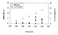
図2はドライエッチング装置のRF出力と銅酸化量およびコンタクト抵抗の関係を示した図である。
図2よりRF出力が増加するにしたがって酸化銅の形成量は増加し、RF出力320W、銅酸化量が10nm以上になったところでコンタクト抵抗のばらつきが大きくなる。これはプラズマ中でイオン化した酸素が半導体基板表面付近に生じたバイアス電圧により加速して銅配線13の中に打ち込まれるため、絶縁層である酸化銅層18が形成するためである。
【0030】
このように、銅酸化量およびコンタクト抵抗はRF出力に敏感なパラメータであることから、半導体装置の製造工程において銅酸化量を実施の形態1で述べた測定方法によりインラインで測定することにより、例えば、銅酸化量が所定の量より多くなったことでRF出力異常であることを検出し、次のプラズマドライエッチング装置のRF出力を調整してコンタクト抵抗のばらつきを抑制する。
【0031】
以上のように実施の形態2によると、銅配線の酸化量をインライン管理で容易に定量化することができ、プラズマドライエッチング装置のRF出力異常の検知にフィードバックしてコンタクト抵抗のばらつきを抑制することができる。
(実施の形態3)
本発明の実施の形態3に係る半導体装置の製造方法について図1,図3,図4を参照しながら説明する。なお、実施の形態3に係る半導体装置の製造方法における工程順の断面構成は、実施の形態1と同様であるが、関係式(2)より銅酸化量の定量化を行い、測定結果を絶縁膜14のエッチング時間にフィードバックする工程を含んでいる。
【0032】
前述のように、図1(d)のドライエッチングによる絶縁膜14を開口する工程において、ドライエッチング後に酸化銅層18が成長している。
図3は絶縁膜のエッチング時間と銅酸化量および絶縁膜残膜の関係を示す図であり、実験において、絶縁膜14のエッチング開始から測定したエッチング時間と、銅配線13の表面が露出した後の銅酸化量および絶縁膜14の残膜の関係を示している。
【0033】
図3において、絶縁膜14のエッチング時間の増加につれ、絶縁膜14の残膜が減少しヴィアホール17bが形成されて銅配線13の表面が露出する。さらにエッチングを続けていくと銅配線13上に酸化銅48が形成され、エッチング時間とともに増加していくことが示されている。しかし、図4に示すように、銅酸化量が増加するにつれコンタクト抵抗ばらつきは増大し、銅酸化量が約10nm以上になるとばらつきは顕著になる。
【0034】
以上の結果から、本実施の形態では、絶縁膜残膜が0(ヴィアホール17bが完全に開口した状態)となり、その後の銅酸化量が0〜約8nmの許容範囲になるように絶縁膜14のエッチング時間を抑制することにより、コンタクト抵抗のばらつきをお抑制するものである。このエッチング時間は以下の関係式(3)から算出することができる。
t=ttyp+{Ttarg e t−(H1−H0)}/RCuO (3)
t(sec):銅酸化量が許容範囲内になるようにフィードバックした後のエッチング時間
ttyp(sec):予め決定された絶縁膜のエッチング時間
Ttarg e t(nm):許容銅酸化量ターゲット値(定数)
(H1−H0)(nm):工程中に測定された銅酸化量
RCuO(nm/min):エッチング中の銅の酸化速度(定数)
上式をさらに説明する。tは予め決定された絶縁膜のエッチング時間で、これは絶縁膜14をちょうどエッチングし終わる時間と、銅配線の表面が露出した後のオーバーエッチング時間との和であり、これが工程中で実際にエッチングした時間となる。(H1−H0)は、実際にエッチングした結果生じた銅酸化量でああるから、Ttarg e t−(H1−H0)は銅酸化量の許容値からのずれであり、RCuOはエッチング中の銅酸化速度であるから{Ttarg e t−(H1−H0)}/RCuOは許容値からのずれに対応するエッチングずれ時間、すなわち銅酸化量を許容銅酸化量に戻すのに必要な時間である。したがって銅酸化量が許容範囲内になるような絶縁膜のエッチング時間は(3)式となる。
【0035】
例えば、工程で実施したエッチング時間ttypを54secとし、銅酸化量ターゲット値Ttarg e tを4nmとし、銅の酸化速度RCuOを1.4nm/sec(図3から算出)とする。図1(d)、(e)で測定した(H1−H0)=2nmとすると、フィードバック後のエッチング時間tは

以上のように、実施の形態3によると、銅配線の酸化量をインライン管理で容易に定量化でき、銅酸化量はプラズマドライエッチング時間に依存することから、銅酸化量を絶縁膜14のエッチング時間制御にフィードバック調整し、このフィードバック調整された絶縁膜のエッチング時間を、次にエッチング処理する半導体基板上に形成された絶縁膜14に適用することにより、酸化量を許容値に設定してコンタクト抵抗のばらつきを防止する事ができる。
【0036】
以上第1から3の実施の形態では金属配線として銅の例を示したが、タングステン、アルミニウム、あるいはそれらを主成分とする材料にも適用することができる。
【0037】
【発明の効果】
以上のように本発明の半導体装置の製造方法によると、ヴィアホール形成工程において、エッチング直後のヴィアホールの深さと、酸化金属膜除去後のヴィアホールの深さを非接触測定法で測定することにより、金属酸化量を製造ライン内で簡便に定量化することができると共に、定量化した結果をエッチング装置のプロセス条件やエッチング時間制御にフィードバックすることにより、コンタクト抵抗のばらつきを抑制することができる。
【図面の簡単な説明】
【図1】(a)本発明のヴィアホールのレジストパターン形成工程を示す工程断面図
(b)本発明のヴィアホール形成工程を示す工程断面図
(c)本発明のレジストパターンを除去する工程を示す工程断面図
(d)本発明の絶縁膜を開口する工程を示す工程断面図
(e)本発明のヴィアホール底面の洗浄工程を示す工程断面図
(f)本発明の金属プラグの形成工程を示す工程断面図
【図2】ドライエッチング装置のRF出力と銅酸化量およびコンタクト抵抗の関係を示した図
【図3】絶縁膜のエッチング時間と銅酸化量および絶縁膜残膜の関係を示す図
【図4】半導体装置の製造における銅酸化量とコンタクト抵抗の関係を示す図
【図5】(a)従来のヴィアホールのレジストパターン形成工程を示す工程断面図
(b)従来のヴィアホール形成工程を示す工程断面図
(c)従来のレジストパターンを除去する工程を示す工程断面図
(d)従来の絶縁膜を開口する工程を示す工程断面図
(e)従来のヴィアホール底面の洗浄工程を示す工程断面図
(f)従来の金属プラグの形成工程を示す工程断面図
【符号の説明】
11 半導体基板
12 絶縁膜
13 銅配線
14 絶縁膜
15 絶縁膜
16 レジストパターン
17 開口部
17a ヴィアホール
17b ヴィアホール
18 酸化銅層
19 金属プラグ
71 半導体基板
72 絶縁膜
73 銅配線
74 絶縁膜
75 絶縁膜
76 レジストパターン
77 開口部
77a ヴィアホール
77b ヴィアホール
78 酸化銅層[0001]
TECHNICAL FIELD OF THE INVENTION
The present invention relates to a method for manufacturing a semiconductor device, and more particularly to a method for manufacturing a wiring structure.
[0002]
[Prior art]
In recent semiconductor integrated circuits, copper having lower resistance than aluminum has been used as a wiring material. In the processing step, a damascene method is used in which a wiring groove is formed in an interlayer insulating film by using a dry etching technique, and a wiring material is embedded in the wiring groove.
[0003]
Hereinafter, a conventional wiring manufacturing method will be described with reference to FIGS.
FIG. 4 is a diagram showing the relationship between the amount of copper oxidation and the contact resistance in the manufacture of a semiconductor device. FIG. 5 is a process sectional view showing a conventional method of manufacturing a semiconductor device using copper wiring, and FIG. 5A is a process sectional view showing a conventional via hole resist pattern forming process, and FIG. ) Is a process sectional view showing a conventional via hole forming process, FIG. 5C is a process sectional view showing a conventional resist pattern removing process, and FIG. 5D is a conventional process for opening an insulating film. FIG. 5E is a process sectional view showing a conventional process of cleaning the bottom surface of a via hole, and FIG. 5F is a process sectional view showing a conventional process of forming a metal plug.
[0004]
First, in a resist pattern forming step shown in FIG. 5A, for example, a
[0005]
Next, in the via hole forming step shown in FIG. 5B, the
[0006]
Next, after the
[0007]
Finally, as shown in FIG. 5 (e), the etching selectivity of copper oxide / copper typified by cleaning containing an organic acid such as ammonium fluoride and ammonium acetate is almost infinite, and the chemical solution of the semiconductor device is almost infinite. After cleaning and removing the
[0008]
As shown in FIG. 5D, when the
[0009]
Conventionally, in order to quantify the amount of oxidation of copper wiring, it has been necessary to perform measurement and evaluation outside the production line, such as SIMS analysis. Therefore, there is a problem that detection takes time even when copper oxidation excessively progresses during the manufacturing process, and process feedback such as dry etching conditions cannot be promptly performed (for example, see Patent Document 1).
[0010]
[Patent Document 1]
Japanese Patent Application Laid-Open No. 2001-208531
[Problems to be solved by the invention]
In order to solve the above problems, a method of manufacturing a semiconductor device according to the present invention aims to easily quantify the amount of copper oxide formed on an underlying copper wiring in a manufacturing line. Further, it is another object of the present invention to feed back the quantified result to the process conditions of the etching apparatus and to control the etching time to suppress the variation in the contact resistance.
[0012]
[Means for Solving the Problems]
The method for manufacturing a semiconductor device according to claim 1 of the present invention includes a step of applying a metal wiring to a circuit formed on a semiconductor substrate, a step of forming an insulating film on the metal wiring, and a plasma dry etching method. Forming a via hole in the insulating film so as to expose the surface portion of the metal wiring by selectively etching the insulating film; and removing a first step between the metal wiring surface portion and the insulating film surface. Measuring by a contact measurement method, washing the metal film surface portion and removing the metal oxide film on the metal film surface portion, and measuring a second step between the metal film surface portion and the insulating film surface. A step of measuring by a non-contact measurement method; and a step of obtaining an oxidation amount of the metal wiring from a difference between the first step and the second step.
[0013]
3. A method for manufacturing a semiconductor device according to claim 2, wherein a step of applying metal wiring to a circuit formed on the semiconductor substrate, a step of forming an insulating film on said metal wiring, and etching including oxygen by a plasma dry etching method. Forming a via hole in the insulating film so as to expose the surface portion of the metal wiring by selectively etching the insulating film with a gas; and forming a first hole between the metal wiring surface portion and the insulating film surface. A step of measuring a step by a non-contact measurement method, a step of removing a metal oxide film on the surface of the metal film using a chemical solution, and a step of non-contacting a second step between the surface of the metal film and the surface of the insulating film. A step of measuring by a measuring method; and a step of obtaining an oxidation amount of the metal wiring from a difference between the first step and the second step.
[0014]
According to a third aspect of the present invention, in the method of manufacturing a semiconductor device according to the second aspect, the metal is copper, and the chemical is an organic acid containing ammonium fluoride.
[0015]
According to a fourth aspect of the present invention, in the method of manufacturing a semiconductor device according to the first, second, or third aspect, the non-contact measurement is performed using an atomic force microscope. And
[0016]
According to a fifth aspect of the present invention, in the method of manufacturing a semiconductor device according to the first, second, or third aspect, the non-contact measurement method is performed by a spectroscopic ellipsometer.
[0017]
A method of manufacturing a semiconductor device according to
[0018]
A method of manufacturing a semiconductor device according to claim 7 is the method of manufacturing a semiconductor device according to claim 1, claim 2, claim 3,
[0019]
According to a eighth aspect of the present invention, in the method of manufacturing a semiconductor device according to the seventh aspect, the etching time is obtained by the following equation (1).
t = t typ + {T targ e t - (H1-H0)} / R CuO (1)
here,
t (sec): optimal etching time H0 obtained (nm): first step H1 (nm): the second step T targ e t (nm): acceptable H1-H0 value t typ: Actual etching time R CuO (nm / min): The amount of copper oxide formed on the underlying copper wiring can be easily quantified in the production line based on the metal oxidation rate during etching or higher. Also, the quantified result can be fed back to the process conditions of the etching apparatus and the control of the etching time to suppress the variation in the contact resistance.
[0020]
BEST MODE FOR CARRYING OUT THE INVENTION
(Embodiment 1)
Hereinafter, a method for manufacturing a semiconductor device according to the first embodiment of the present invention will be described with reference to FIGS.
[0021]
FIG. 1 is a process sectional view showing a method for manufacturing a semiconductor device using copper wiring of the present invention. FIG. 1 (a) is a process sectional view showing a via hole resist pattern forming process of the present invention, and FIG. 1) is a process sectional view showing a via hole forming process of the present invention, FIG. 1 (c) is a process sectional view showing a process of removing the resist pattern of the present invention, and FIG. 1 (d) is an opening of the insulating film of the present invention. FIG. 1E is a sectional view showing a step of cleaning the bottom surface of the via hole of the present invention, and FIG. 1F is a sectional view showing a step of forming a metal plug of the present invention.
[0022]
First, in a resist pattern forming step shown in FIG. 1A, a
[0023]
Next, in the via hole forming step shown in FIG. 1B, the insulating
[0024]
Next, after removing the resist
[0025]
Next, as shown in FIG. 1 (e), the etching selectivity of
[0026]
The process is completed as described above. Here, the thickness of the
(Copper oxide layer 18) = (H1)-(H0) (2)
As described above, according to the first embodiment, in the step of forming the copper wiring of the semiconductor device, the level of oxidation of the copper wiring is easily quantified by measuring the step by the non-contact method called AFM before and after the formation of the
[0027]
For example, one semiconductor substrate being manufactured is taken out, and H0 and H1 are measured for ten contacts of the process monitor pattern formed on the scribe lane. If the thickness is 7 nm or less, the process can be continued, and if the thickness is 7 nm or more, measures such as changing dry etching conditions can be taken.
[0028]
Note that, in this embodiment, a method for quantifying the amount of copper oxidation after the plasma dry etching step is described. However, if copper oxidation occurs in the plasma ashing step using oxygen plasma, the amount of copper oxidation is similarly determined using this method. Can be quantified. Although copper is used as the wiring material in the present embodiment, the same effect can be obtained with a W wiring or an Al wiring. Further, in this embodiment, the AFM is used for measuring the steps H0 and H1, but the same measurement is possible because the spectroscopic ellipsometer can measure the thickness of the copper oxide film without contact.
(Embodiment 2)
Hereinafter, a method for manufacturing a semiconductor device according to the second embodiment of the present invention will be described with reference to FIGS. Note that the manufacturing process in the present embodiment is the same as that described in Embodiment 1, and as described above, in the step of opening the insulating
[0029]
FIG. 2 is a diagram showing the relationship between the RF output of the dry etching apparatus, the amount of copper oxidation, and the contact resistance.
As shown in FIG. 2, as the RF output increases, the formation amount of copper oxide increases. When the RF output becomes 320 W and the copper oxidation amount becomes 10 nm or more, the variation in the contact resistance increases. This is because oxygen ionized in the plasma is accelerated by a bias voltage generated near the surface of the semiconductor substrate and is driven into the
[0030]
As described above, since the copper oxidation amount and the contact resistance are parameters sensitive to the RF output, by measuring the copper oxidation amount in-line by the measuring method described in the first embodiment in the semiconductor device manufacturing process, for example, Then, it is detected that the RF output is abnormal because the copper oxidation amount has exceeded the predetermined amount, and the RF output of the next plasma dry etching apparatus is adjusted to suppress the variation in the contact resistance.
[0031]
As described above, according to the second embodiment, the oxidation amount of the copper wiring can be easily quantified by in-line management, and the variation in the contact resistance is suppressed by feeding back to the detection of the RF output abnormality of the plasma dry etching apparatus. be able to.
(Embodiment 3)
Third Embodiment A method for manufacturing a semiconductor device according to a third embodiment of the present invention will be described with reference to FIGS. The cross-sectional structure in the order of steps in the method of manufacturing the semiconductor device according to the third embodiment is the same as that of the first embodiment, but the amount of copper oxidation is quantified by the relational expression (2), and the measurement result is insulated. It includes a step of feeding back the etching time of the
[0032]
As described above, in the step of opening the insulating
FIG. 3 is a diagram showing the relationship between the etching time of the insulating film, the amount of copper oxidation, and the remaining film of the insulating film. In the experiment, the etching time measured from the start of the etching of the insulating
[0033]
In FIG. 3, as the etching time of the insulating
[0034]
From the above results, in the present embodiment, the insulating
t = t typ + {T targ e t - (H1-H0)} / R CuO (3)
t (sec): copper etching after the oxidation amount is fed back to be within the acceptable time range t typ (sec): the etching time of predetermined insulating film T targ e t (nm): allowable amount of copper oxidation target Value (constant)
(H1-H0) (nm): Copper oxidation amount measured during the process R CuO (nm / min): Copper oxidation rate during etching (constant)
The above equation is further explained. t is a predetermined etching time of the insulating film, which is a sum of a time when the etching of the insulating
[0035]
For example, the etching time t typ which was carried out in step a 54Sec, copper oxide amount target value T targ e t and 4 nm, the oxidation rate R CuO of copper and 1.4 nm / sec (calculated from Fig. 3). Assuming that (H1−H0) = 2 nm measured in FIGS. 1D and 1E, the etching time t after feedback is
As described above, according to the third embodiment, the oxidation amount of the copper wiring can be easily quantified by in-line management, and the copper oxidation amount depends on the plasma dry etching time. Feedback control is performed for time control, and the feedback adjusted etching time of the insulating film is applied to the insulating
[0036]
As described above, in the first to third embodiments, copper is used as an example of the metal wiring. However, the present invention can be applied to tungsten, aluminum, or a material containing these as main components.
[0037]
【The invention's effect】
As described above, according to the method for manufacturing a semiconductor device of the present invention, in the via hole forming step, the depth of the via hole immediately after etching and the depth of the via hole after removing the metal oxide film are measured by a non-contact measurement method. Thereby, the amount of metal oxidation can be easily quantified in the production line, and the quantified result can be fed back to the process conditions of the etching apparatus and the control of the etching time, thereby suppressing the variation in the contact resistance. .
[Brief description of the drawings]
FIG. 1A is a process sectional view showing a via hole resist pattern forming step of the present invention. FIG. 1B is a process sectional view showing a via hole forming step of the present invention. FIG. (D) Step sectional view showing a step of opening an insulating film of the present invention (e) Step sectional view showing a step of cleaning the bottom surface of a via hole of the present invention (f) Step of forming a metal plug of the present invention FIG. 2 is a diagram showing the relationship between the RF output of the dry etching apparatus and the amount of copper oxidation and the contact resistance. FIG. 3 is a diagram showing the relationship between the etching time of the insulating film, the amount of copper oxidation and the remaining film of the insulating film. FIG. 4 is a view showing the relationship between the amount of copper oxidation and the contact resistance in the manufacture of a semiconductor device. FIG. 5 (a) is a process sectional view showing a conventional via hole resist pattern forming process, and (b) is a conventional via hole type. (C) Step sectional view showing a step of removing a conventional resist pattern. (D) Step sectional view showing a step of opening a conventional insulating film. (E) Conventional step of cleaning the bottom surface of a via hole. (F) Process cross-sectional view showing a conventional metal plug forming process.
Claims (8)
前記金属配線の上に絶縁膜を形成する工程と、
プラズマドライエッチング法により前記絶縁膜を選択的にエッチングして前記金属配線の表面部を露出するように前記絶縁膜にヴィアホールを形成する工程と、
前記金属配線表面部と前記絶縁膜表面との第1の段差を非接触測定法で測定する工程と、
前記金属膜表面部を洗浄して前記金属膜表面部の酸化金属膜を除去する工程と、
前記金属膜表面部と前記絶縁膜表面との第2の段差を非接触測定法で測定する工程と、
前記第1の段差と第2の段差の差より前記金属配線の酸化量を求める工程と
を有することを特徴とする半導体装置の製造方法。Applying metal wiring to a circuit formed on a semiconductor substrate;
Forming an insulating film on the metal wiring,
Forming a via hole in the insulating film so as to selectively etch the insulating film by a plasma dry etching method to expose a surface portion of the metal wiring;
Measuring a first step between the metal wiring surface portion and the insulating film surface by a non-contact measurement method;
Removing the metal oxide film on the surface of the metal film by cleaning the surface of the metal film;
Measuring a second step between the metal film surface and the insulating film surface by a non-contact measurement method;
Obtaining the oxidation amount of the metal wiring from the difference between the first step and the second step.
前記金属配線の上に絶縁膜を形成する工程と、
プラズマドライエッチング法により酸素を含むエッチングガスで前記絶縁膜を選択的にエッチングして前記金属配線の表面部を露出するように前記絶縁膜にヴィアホールを形成する工程と、
前記金属配線表面部と前記絶縁膜表面との第1の段差を非接触測定法で測定する工程と、
前記金属膜表面部の酸化金属膜を薬液を用いて除去する工程と、
前記金属膜表面部と前記絶縁膜表面との第2の段差を非接触測定法で測定する工程と、
前記第1の段差と第2の段差の差より前記金属配線の酸化量を求める工程と
を有することを特徴とする半導体装置の製造方法。Applying metal wiring to a circuit formed on a semiconductor substrate;
Forming an insulating film on the metal wiring,
Forming a via hole in the insulating film so as to selectively etch the insulating film with an etching gas containing oxygen by a plasma dry etching method to expose a surface portion of the metal wiring;
Measuring a first step between the metal wiring surface portion and the insulating film surface by a non-contact measurement method;
Removing the metal oxide film on the surface of the metal film using a chemical solution,
Measuring a second step between the metal film surface and the insulating film surface by a non-contact measurement method;
Obtaining the oxidation amount of the metal wiring from the difference between the first step and the second step.
t=ttyp+{Ttarg e t−(H1−H0)}/RCuO (1)
ここで、
t(sec):求められる最適なエッチング時間
H0(nm):第1の段差
H1(nm):第2の段差
Ttarg e t(nm):許容されるH1−H0値
ttyp:実績エッチング時間
RCuO(nm/min):エッチング中の金属酸化速度8. The method according to claim 7, wherein the etching time is obtained by the following equation (1).
t = t typ + {T targ e t - (H1-H0)} / R CuO (1)
here,
t (sec): optimal etching time H0 obtained (nm): first step H1 (nm): the second step T targ e t (nm): acceptable H1-H0 value t typ: Actual etching time R CuO (nm / min): metal oxidation rate during etching
Priority Applications (2)
| Application Number | Priority Date | Filing Date | Title |
|---|---|---|---|
| JP2003133837A JP2004342632A (en) | 2003-05-13 | 2003-05-13 | Method of manufacturing semiconductor device |
| US10/843,364 US6869810B2 (en) | 2003-05-13 | 2004-05-12 | Manufacturing method of semiconductor device |
Applications Claiming Priority (1)
| Application Number | Priority Date | Filing Date | Title |
|---|---|---|---|
| JP2003133837A JP2004342632A (en) | 2003-05-13 | 2003-05-13 | Method of manufacturing semiconductor device |
Publications (1)
| Publication Number | Publication Date |
|---|---|
| JP2004342632A true JP2004342632A (en) | 2004-12-02 |
Family
ID=33410656
Family Applications (1)
| Application Number | Title | Priority Date | Filing Date |
|---|---|---|---|
| JP2003133837A Pending JP2004342632A (en) | 2003-05-13 | 2003-05-13 | Method of manufacturing semiconductor device |
Country Status (2)
| Country | Link |
|---|---|
| US (1) | US6869810B2 (en) |
| JP (1) | JP2004342632A (en) |
Cited By (3)
| Publication number | Priority date | Publication date | Assignee | Title |
|---|---|---|---|---|
| JP2012028357A (en) * | 2010-07-20 | 2012-02-09 | Hitachi High-Technologies Corp | Plasma processing apparatus and plasma processing method |
| WO2015146023A1 (en) * | 2014-03-25 | 2015-10-01 | 株式会社Joled | Etching method and organic el display panel manufacturing method using same |
| JP2021007151A (en) * | 2010-02-26 | 2021-01-21 | 株式会社半導体エネルギー研究所 | Liquid crystal display device |
Families Citing this family (10)
| Publication number | Priority date | Publication date | Assignee | Title |
|---|---|---|---|---|
| US6303500B1 (en) * | 1999-02-24 | 2001-10-16 | Micron Technology, Inc. | Method and apparatus for electroless plating a contact pad |
| US7299151B2 (en) * | 2004-02-04 | 2007-11-20 | Hewlett-Packard Development Company, L.P. | Microdevice processing systems and methods |
| JP2005347587A (en) * | 2004-06-04 | 2005-12-15 | Sony Corp | Cleaning liquid composition after dry etching, and manufacturing method of semiconductor device |
| US7259463B2 (en) * | 2004-12-03 | 2007-08-21 | Taiwan Semiconductor Manufacturing Company, Ltd. | Damascene interconnect structure with cap layer |
| US20070184666A1 (en) * | 2006-02-08 | 2007-08-09 | Texas Instruments Inc. | Method for removing residue containing an embedded metal |
| DE102007004860B4 (en) * | 2007-01-31 | 2008-11-06 | Advanced Micro Devices, Inc., Sunnyvale | A method of making a copper-based metallization layer having a conductive overcoat by an improved integration scheme |
| JP2009027048A (en) * | 2007-07-23 | 2009-02-05 | Panasonic Corp | Manufacturing method of semiconductor device |
| KR20100051211A (en) * | 2008-11-07 | 2010-05-17 | 주식회사 동부하이텍 | Method for manufacturing a metal line of an image sensor |
| US9437540B2 (en) * | 2014-09-12 | 2016-09-06 | Taiwan Semiconductor Manufacturing Company, Ltd. | Additional etching to increase via contact area |
| US9887160B2 (en) * | 2015-09-24 | 2018-02-06 | International Business Machines Corporation | Multiple pre-clean processes for interconnect fabrication |
Family Cites Families (4)
| Publication number | Priority date | Publication date | Assignee | Title |
|---|---|---|---|---|
| JPH02124406A (en) | 1988-11-01 | 1990-05-11 | Mitsubishi Electric Corp | Semiconductor manufacturing apparatus |
| JP2978748B2 (en) * | 1995-11-22 | 1999-11-15 | 日本電気株式会社 | Method for manufacturing semiconductor device |
| US5888906A (en) * | 1996-09-16 | 1999-03-30 | Micron Technology, Inc. | Plasmaless dry contact cleaning method using interhalogen compounds |
| US6313042B1 (en) * | 1999-09-03 | 2001-11-06 | Applied Materials, Inc. | Cleaning contact with successive fluorine and hydrogen plasmas |
-
2003
- 2003-05-13 JP JP2003133837A patent/JP2004342632A/en active Pending
-
2004
- 2004-05-12 US US10/843,364 patent/US6869810B2/en not_active Expired - Fee Related
Cited By (6)
| Publication number | Priority date | Publication date | Assignee | Title |
|---|---|---|---|---|
| JP2021007151A (en) * | 2010-02-26 | 2021-01-21 | 株式会社半導体エネルギー研究所 | Liquid crystal display device |
| US11049733B2 (en) | 2010-02-26 | 2021-06-29 | Semiconductor Energy Laboratory Co., Ltd. | Method for manufacturing semiconductor device |
| JP2022023883A (en) * | 2010-02-26 | 2022-02-08 | 株式会社半導体エネルギー研究所 | Liquid crystal display device |
| US11682562B2 (en) | 2010-02-26 | 2023-06-20 | Semiconductor Energy Laboratory Co., Ltd. | Method for manufacturing semiconductor device |
| JP2012028357A (en) * | 2010-07-20 | 2012-02-09 | Hitachi High-Technologies Corp | Plasma processing apparatus and plasma processing method |
| WO2015146023A1 (en) * | 2014-03-25 | 2015-10-01 | 株式会社Joled | Etching method and organic el display panel manufacturing method using same |
Also Published As
| Publication number | Publication date |
|---|---|
| US6869810B2 (en) | 2005-03-22 |
| US20040229389A1 (en) | 2004-11-18 |
Similar Documents
| Publication | Publication Date | Title |
|---|---|---|
| US6849559B2 (en) | Method for removing photoresist and etch residues | |
| US7169440B2 (en) | Method for removing photoresist and etch residues | |
| JP5193604B2 (en) | Method for removing low pressure of photoresist and etching residue | |
| US6232209B1 (en) | Semiconductor device and manufacturing method thereof | |
| US6849556B2 (en) | Etching method, gate etching method, and method of manufacturing semiconductor devices | |
| US7700494B2 (en) | Low-pressure removal of photoresist and etch residue | |
| JP2004342632A (en) | Method of manufacturing semiconductor device | |
| US7786005B2 (en) | Method for manufacturing semiconductor device to form a via hole | |
| TWI404140B (en) | Dry etching method | |
| JP3643580B2 (en) | Plasma processing apparatus and semiconductor manufacturing apparatus | |
| US6756241B2 (en) | Method of manufacturing semiconductor device and system for manufacturing the same | |
| JP2004503104A (en) | Feedback control of strip time to reduce post-strip critical dimension variation of transistor gate electrode | |
| US7709393B2 (en) | Method for manufacturing semiconductor device | |
| JP2004253516A (en) | Dry etching method and apparatus for test sample | |
| US8492174B2 (en) | Etch tool process indicator method and apparatus | |
| JP4745273B2 (en) | Semiconductor device manufacturing method and semiconductor manufacturing apparatus | |
| US20130071955A1 (en) | Plasma etching method | |
| WO2010110878A1 (en) | Plasma etching method | |
| JP3527165B2 (en) | Contact hole formation method | |
| Lercel et al. | Etching processes and characteristics for the fabrication of refractory x-ray masks | |
| JP3123499B2 (en) | How to monitor dry etching | |
| JP2006073701A (en) | Method for monitoring etching process | |
| US20050136335A1 (en) | Patterned microelectronic mask layer formation method employing multiple feed-forward linewidth measurement | |
| JP2000269220A (en) | Manufacture of semiconductor device | |
| JP2000182968A (en) | Semiconductor device and manufacture thereof |