JP2004335524A - Light emitting diode - Google Patents
Light emitting diode Download PDFInfo
- Publication number
- JP2004335524A JP2004335524A JP2003125078A JP2003125078A JP2004335524A JP 2004335524 A JP2004335524 A JP 2004335524A JP 2003125078 A JP2003125078 A JP 2003125078A JP 2003125078 A JP2003125078 A JP 2003125078A JP 2004335524 A JP2004335524 A JP 2004335524A
- Authority
- JP
- Japan
- Prior art keywords
- transparent member
- light emitting
- light
- refractive index
- emitting element
- Prior art date
- Legal status (The legal status is an assumption and is not a legal conclusion. Google has not performed a legal analysis and makes no representation as to the accuracy of the status listed.)
- Pending
Links
Images


Classifications
-
- H—ELECTRICITY
- H01—ELECTRIC ELEMENTS
- H01L—SEMICONDUCTOR DEVICES NOT COVERED BY CLASS H10
- H01L2224/00—Indexing scheme for arrangements for connecting or disconnecting semiconductor or solid-state bodies and methods related thereto as covered by H01L24/00
- H01L2224/01—Means for bonding being attached to, or being formed on, the surface to be connected, e.g. chip-to-package, die-attach, "first-level" interconnects; Manufacturing methods related thereto
- H01L2224/42—Wire connectors; Manufacturing methods related thereto
- H01L2224/47—Structure, shape, material or disposition of the wire connectors after the connecting process
- H01L2224/48—Structure, shape, material or disposition of the wire connectors after the connecting process of an individual wire connector
- H01L2224/4805—Shape
- H01L2224/4809—Loop shape
- H01L2224/48091—Arched
Landscapes
- Led Device Packages (AREA)
Abstract
Description
【0001】
【発明の属する技術分野】
本発明は、照明装置などに用いる発光ダイオードに関するものである。
【0002】
【従来の技術】
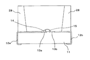
一般に、チップ型の発光ダイオードは、携帯電話や小型電子機器の液晶表示部のバックライト光源や各種の照明装置の光源として広く利用されている。図5は従来の発光ダイオードの側面図である。ベース基板11と反射部材28とは白色の樹脂で一体的に形成され、ベース基板11の左右両側に金属製リードフレーム12a、12bを設け、一方のリードフレーム12aに形成される第1電極部13aに発光素子14を搭載し、他方のリードフレーム12bに形成される第2電極部13bに金属製ワイヤ15で接続する。そして、この金属製ワイヤおよび発光素子14の上部を透明の樹脂製パッケージで被覆する。
【0003】
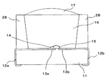
このように、ベース基板11上に配置された金属製リードフレーム12aの第1電極部13aに半導体チップである発光素子14を配設し、この発光素子14を透明な樹脂16で充填して樹脂製パッケージ内に発光素子14を封止して発光ダイオードを形成していた。また、配光角を小さくする場合には、図6に示すように透明樹脂15の前面に凸レンズ17を配設し、発光素子14からの光線を前面の凸レンズ17で屈折させて配光角の調整を行っていた。
【0004】
【発明が解決しようとする課題】
しかし、凸レンズ17で集光させる場合などでは、発光素子14と凸レンズ17との間の距離が凸レンズ17のR面の半径以上必要となることから、厚みが増すと言った問題がある。
【0005】
本発明の目的は、発光ダイオードの厚みを増加させることなく配光角を調整できる発光ダイオードを提供することである。
【0006】
【課題を解決するための手段】
請求項1の発明に係わる発光ダイオードは、電極部が形成されたベース基板上に設置された発光素子と;前記発光素子の上部を被覆し前記ベース基板との間に第1空気層を形成し前記発光素子に対面する反対側に凸部を有した第1透明部材と;前記第1透明部材に対面する側に前記第1透明部材の凸部に嵌合する凹部と前記第1透明部材との間に第2空気層を形成する凹部とが複合された面を有した第2透明部材と;前記第2透明部材の前記第1透明部材に対面する反対側に形成された円環状の凸レンズと;を備えたことを特徴とする。
【0007】
本発明及び以下の発明において、特に指定しない限り用語の定義及び技術的意味は以下による。
【0008】
ベース基板は白色の樹脂で反射部材と一体的に形成され、電極部はリードフレームと一体的に形成される。そして、白色樹脂とリードフレームとは一体モールド化される。発光素子は半導体チップであり、電極部から電源が供給されたときに発光する素子である。
【0009】
第1透明部材は、透明樹脂で形成され発光素子の上部を被覆し、ベース基板との間に第1空気層を形成する。また、発光素子に対面する反対側には凸部を有している。第2透明部材は、透明樹脂で形成され第1透明部材に対面する側に第1透明部材の凸部に嵌合する凹部を有すると共に、第1透明部材との間に第2空気層を形成する凹部とを有する。また、第2透明部材の第1透明部材に対面する反対側には円環状の凸レンズが形成され、この円環状凸レンズで光線を集光し外部に外部に光線を出射する。
【0010】
従って、第1透明部材と第2透明部材とが接触する境界面は、第1透明部材の凸部と第2透明部材の凹部との嵌合部分と、第2空気槽が形成された部分とを有した複合面となる。発光素子からの光線は第1透明部材と第2透明部材とが接触する境界面に入射され、その境界面の第2空気層の底部に当たった光線は全反射して第1空気層に入射され、第1空気層でさらに全反射して第1透明部材と第2透明部材とが接触する境界面に入射される。一方、第1透明部材と第2透明部材とが接触する境界面の第1透明部材の凸部と第2透明部材の凹部との嵌合部分に当たった光線は、その嵌合部を通過して第2透明部材に入り、第2空気層の傾斜面で全反射し円環状凸レンズで集光されて外部に出射される。
【0011】
本発明によれば、全反射を利用していることから反射のロスは小さく、また配光角を調整するには、前面の円環状凸レンズの曲率半径を変化させるか第2空気層を作る凹部の傾斜角を変化させることで可能であるので、発光素子からの光線を減衰させることなく、また、発光ダイオードの厚みを増加させることなく配光角を容易に調整できる発光ダイオードを提供できる。
【0012】
請求項2の発明に係わる発光ダイオードは、請求項1の発明において、前記第1空気層および前記第2空気層に代えて屈折率1以上1.45未満の低屈折率材料層を配設し、前記第1透明部材および前記第2透明部材を屈折率1.45以上2未満の高屈折率材料層で一体的に形成したことを特徴とする。
【0013】
本発明は、第1空気層および第2空気層に代えて屈折率1以上1.45未満の低屈折率材料層を配設し、第1透明部材および第2透明部材を屈折率1.45以上2未満の高屈折率材料層で一体的に形成したものである。
【0014】
本発明によれば、高屈折率材料層の内部に屈折率1以上1.45未満の傾斜を持った低屈折率材料層を含ませるので、高屈折率材料層27は一体的に形成され重なる部分がないので、請求項1の発明の効果に加え、さらに光線の出射効率が向上する。
【0015】
【発明の実施の形態】
以下、本発明の実施の形態を説明する。図1は本発明の第1の実施の形態に係わる発光ダイオードの説明図であり、図1(a)は平面図、図1(b)は側面図である。ベース基板11と反射部材28とは白色の樹脂で一体的に形成され、ベース基板11の左右両側に金属製リードフレーム12a、12bが取り付けられる。そして、一方のリードフレーム12aに形成される第1電極部13aに発光素子14が搭載して接続され、他方のリードフレーム12bに形成される第2電極部13bと金属製ワイヤ15で接続される。これにより、発光素子14に電源が供給されるようにしている。
【0016】
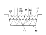
発光素子14の上部は第1透明部材18で被覆される。その際に、第1透明部材18とベース基板11(リードフレーム12)との間に第1空気層19を形成する。また、第1透明部材18の発光素子14に対面する反対側には凸部20が形成されている。さらに、この第1透明部材18の上部は第2透明部材21が被覆される。第2透明部材21の第1透明部材18に対面する側には、第1透明部材18の凸部20に嵌合する凹部22が設けられ、また、第2透明部材21と第1透明部材18との間に第2空気層23を形成するための凹部24が設けられている。一方、第2透明部材21の第1透明部材18に対面する反対側には円環状凸レンズ25が設けられている。この円環状凸レンズ25は集光性を増すために設けられている。
【0017】
このように、点光源である発光素子14の周囲に第1空気層19を設け、また、第1空気層19の反対側に円環状の突起(凸部20)をある間隔で配置した第1透明部材18を配設し、その第1透明部材18の突起(凸部20)と同じ形状の凹部22および第2空気層23を形成する凹部24とを有した第2透明部材21を重ねていき、第1透明部材18の凸部20と第2透明部材21の凹部22とを嵌合させると共に、第2空気層23を形成する。
【0018】
従って、第1透明部材18と第2透明部材21とが接触する境界面は、第1透明部材18の凸部20と第2透明部材21の凹部22との嵌合部分と、第2空気層23が形成された部分との複合面となる。また、第2透明部材21の出光側には配光角を調整するための円環状凸レンズ25が設けられている。
【0019】
図2は、第1の実施の形態における発光素子14からの光線が円環状凸レンズ25からどのように出射されるかを示した光線追跡図である。光線は大きく分けて2つの動きをする。まず、一つ目は、発光素子14からの光線が第2空気層23の底部に当たった場合であり、この場合には光線は第2空気層23で全反射することになり、発光素子14側の面に向く光線となる。そして、発光素子14側の第1空気層19でも全反射することになり、この反射光が再度第2空気層23に当たれば同じことを繰り返す。
【0020】
次に、2つ目は凸部20と凹部22とが重なり合った部分に光線があたる場合であり、この場合には、その部分からの光線が前面の第2透明部材21に入り込み、第2空気層23を作る傾斜の部分に当たって全反射することになり、全反射した光は円環状凸レンズ25を通って外部に出射する。なお、円環状凸レンズ25は集光性を増すために利用している。
【0021】
第1の実施の形態によれば、発光素子14からの光線は第1の空気層19および第2の空気層23での全反射を利用し、最終的に円環状凸レンズ25で集光して外部に光線を出射するようにしているので、全体として反射のロスが小さい。また、配光角を調整するには、前面の円環状凸レンズ25の曲率半径を変化させるか第2空気層23を形成する凹部24の傾斜角を変化させることで可能になるので容易に配光角を調整できる。
次に、本発明の第2の実施の形態を説明する。図3は本発明の第2の実施の形態に係わる発光ダイオードの説明図であり、図3(a)は平面図、図3(b)は側面図である。この第2の実施の形態は、図1に示した第1の実施の形態に対し、第1空気層19および第2空気層23に代えて屈折率1以上1.45未満の低屈折率材料層26a、26bを配設し、第1透明部材18および第2透明部材21を屈折率1.45以上2未満の高屈折率材料層27で一体的に形成したものである。図1に示し第1の実施の形態と同一要素には同一符号を付し重複する説明は省略する。
【0022】
図3において、ベース基材11のリードフレーム12aの第1電極部13aに配置された発光素子14の周囲に、第1空気層19に代えて低屈折率材料層26aを形成し、その上部に高屈折率材料層27を形成する。高屈折材料層27は、高屈折率材料の中に低屈折率材料を埋め込んで、高屈折率材料層27の内部に低屈折率材料層26bを形成し、第1透明部材18および第2透明部材21を一体的に形成している。低屈折率材料層26a、26bは、屈折率が1以上で1.45未満の低屈折率材料を使用し、高屈折率材料層27としては屈折率1.45以上2未満の高屈折率材料を使用する。
【0023】
図4は、第2の実施の形態における発光素子14からの光線が円環状凸レンズ25からどのように出射されるかを示した光線追跡図である。第1の実施の形態の場合と同様に、光線は大きく分けて2つの動きをする。まず、一つ目は、発光素子14からの光線が低屈折率材料層26bの底部に当たった場合であり、この場合には光線は低屈折率材料層26bで全反射することになり、発光素子14側の面に向く光線となる。そして、発光素子14側の低屈折率材料層26aでも全反射することになり、この反射光が、再度低屈折率材料層26bに当たれば同じことを繰り返す。次に、2つ目は、低屈折率材料層26bの傾斜面部に光線があたる場合で、この場合には、低屈折率材料層26bを作る傾斜面部に当たって全反射することになり、全反射した光は円環状凸レンズ25を通って外部に出射する。
【0024】
図4では、高屈折率材料層27は一体的に形成されており重なる部分がないことから、この重なり部分のロスがなくなり効率はさらに向上する。この場合にも配光角を調整するには、前面の円環状凸レンズ25の曲率半径を変化させるか埋め込んだ低屈折率材料層26bの傾斜角を変化させることで可能になる。
【0025】
第2の実施の形態によれば、発光素子14からの光線は低屈折率材料層26a、26bでの全反射を利用し、最終的に円環状凸レンズ25で集光して外部に光線を出射するようにしているので全体として反射のロスが小さい。また、高屈折率材料層27は一体的に形成されており重なる部分がないことから、効率はさらに良くなる。また、配光角を調整するには、前面の円環状凸レンズ25の曲率半径を変化させるか低屈折率材料層26bを形成する凹部24の傾斜角を変化させることで可能になるので容易に配光角を調整できる。
【0026】
【発明の効果】
以上述べたように、請求項1の発明によれば、全反射を利用していることから反射のロスは小さく、また配光角を調整するには、前面の円環状凸レンズの曲率半径を変化させるか第2空気層を作る凹部の傾斜角を変化させることで可能であるので、発光素子からの光線を減衰させることなく、また、発光ダイオードの厚みを増加させることなく配光角を容易に調整できる発光ダイオードを提供できる。
【0027】
また、請求項2の発明によれば、高屈折率材料層の内部に屈折率1以上1.45未満の傾斜を持った低屈折率材料層を含ませるので、高屈折率材料層27は一体的に形成され重なる部分がないので、請求項1の発明の効果に加え、さらに光線の出射効率が向上する。
【図面の簡単な説明】
【図1】本発明の第1の実施の形態に係わる発光ダイオードの説明図。
【図2】本発明の第1の実施の形態における発光素子からの光線が円環状凸レンズからどのように出射されるかを示した光線追跡図。
【図3】本発明の第2の実施の形態に係わる発光ダイオードの説明図。
【図4】本発明の第2の実施の形態における発光素子からの光線が円環状凸レンズからどのように出射されるかを示した光線追跡図。
【図5】従来の発光ダイオードの側面図。
【図6】従来の凸レンズを有した発光ダイオードの側面図。
【符号の説明】
11…ベース基板、12a…金属製リードフレーム、13a…第1電極部、13b…第2電極部、14…発光素子、15…金属製ワイヤ、16…透明樹脂、17…凸レンズ、18…第1透明部材、19…第1空気層、20…凸部、21…第2透明部材、22…凹部、23…第2空気層、24…凹部、25…円環状凸レンズ、26…低屈折率材料層、27…高屈折率材料層、28…反射部材[0001]
TECHNICAL FIELD OF THE INVENTION
The present invention relates to a light emitting diode used for a lighting device and the like.
[0002]
[Prior art]
2. Description of the Related Art In general, chip-type light emitting diodes are widely used as backlight light sources for liquid crystal display units of mobile phones and small electronic devices and light sources of various lighting devices. FIG. 5 is a side view of a conventional light emitting diode. The
[0003]
As described above, the
[0004]
[Problems to be solved by the invention]
However, when the light is condensed by the
[0005]
An object of the present invention is to provide a light emitting diode that can adjust a light distribution angle without increasing the thickness of the light emitting diode.
[0006]
[Means for Solving the Problems]
A light emitting diode according to the first aspect of the present invention includes a light emitting device disposed on a base substrate on which an electrode portion is formed; and forming a first air layer between the light emitting device and an upper portion of the light emitting device and the base substrate. A first transparent member having a convex portion on the opposite side facing the light emitting element; a concave portion fitted to the convex portion of the first transparent member on a side facing the first transparent member; and the first transparent member; A second transparent member having a surface in which a concave portion forming a second air layer is interposed therebetween; and an annular convex lens formed on a side of the second transparent member opposite to the first transparent member. And;
[0007]
In the present invention and the following inventions, definitions and technical meanings of terms are as follows unless otherwise specified.
[0008]
The base substrate is formed integrally with the reflection member using white resin, and the electrode portion is formed integrally with the lead frame. Then, the white resin and the lead frame are integrally molded. The light emitting element is a semiconductor chip, which emits light when power is supplied from the electrode portion.
[0009]
The first transparent member is formed of a transparent resin, covers an upper part of the light emitting element, and forms a first air layer between the first transparent member and the base substrate. Further, a convex portion is provided on the opposite side facing the light emitting element. The second transparent member is formed of a transparent resin, has a concave portion on the side facing the first transparent member, the concave portion being fitted to the convex portion of the first transparent member, and forms a second air space between the second transparent member and the first transparent member. And a concave portion. Further, an annular convex lens is formed on the opposite side of the second transparent member facing the first transparent member. The annular convex lens collects light rays and emits light rays to the outside.
[0010]
Therefore, the boundary surface where the first transparent member and the second transparent member are in contact with each other includes a fitting portion between the convex portion of the first transparent member and the concave portion of the second transparent member, and a portion where the second air tank is formed. Is obtained. Light rays from the light emitting element are incident on a boundary surface where the first transparent member and the second transparent member are in contact with each other, and light rays hitting the bottom of the second air layer at the boundary surface are totally reflected and incident on the first air layer. Then, the light is further totally reflected by the first air layer and is incident on a boundary surface where the first transparent member and the second transparent member come into contact with each other. On the other hand, a light beam hitting a fitting portion between the convex portion of the first transparent member and the concave portion of the second transparent member at the boundary surface where the first transparent member and the second transparent member come into contact passes through the fitting portion. And enters the second transparent member, is totally reflected by the inclined surface of the second air layer, is condensed by the annular convex lens, and is emitted to the outside.
[0011]
According to the present invention, since the total reflection is used, the reflection loss is small, and in order to adjust the light distribution angle, the radius of curvature of the front annular convex lens is changed or the concave portion for forming the second air layer is formed. It is possible to provide a light-emitting diode that can easily adjust the light distribution angle without attenuating the light rays from the light-emitting element and without increasing the thickness of the light-emitting diode.
[0012]
According to a second aspect of the present invention, in the light emitting diode according to the first aspect, a low refractive index material layer having a refractive index of 1 or more and less than 1.45 is provided in place of the first air layer and the second air layer. The first transparent member and the second transparent member are integrally formed of a high refractive index material layer having a refractive index of 1.45 or more and less than 2.
[0013]
According to the present invention, a low refractive index material layer having a refractive index of 1 or more and less than 1.45 is provided in place of the first air layer and the second air layer, and the first transparent member and the second transparent member are provided with a refractive index of 1.45. More than two and less than two high refractive index material layers are integrally formed.
[0014]
According to the present invention, the high-refractive-
[0015]
BEST MODE FOR CARRYING OUT THE INVENTION
Hereinafter, embodiments of the present invention will be described. FIG. 1 is an explanatory view of a light emitting diode according to a first embodiment of the present invention. FIG. 1 (a) is a plan view and FIG. 1 (b) is a side view. The
[0016]
The upper part of the
[0017]
As described above, the
[0018]
Therefore, the boundary surface where the first
[0019]
FIG. 2 is a ray tracing diagram showing how rays from the
[0020]
Next, the second is a case where a light beam hits a portion where the
[0021]
According to the first embodiment, the light rays from the
Next, a second embodiment of the present invention will be described. FIG. 3 is an explanatory view of a light emitting diode according to a second embodiment of the present invention. FIG. 3 (a) is a plan view and FIG. 3 (b) is a side view. This second embodiment is different from the first embodiment shown in FIG. 1 in that a low refractive index material having a refractive index of 1 or more and less than 1.45 is used instead of the
[0022]
In FIG. 3, a low-refractive-
[0023]
FIG. 4 is a ray tracing diagram showing how rays from the
[0024]
In FIG. 4, since the high-refractive-
[0025]
According to the second embodiment, the light beam from the
[0026]
【The invention's effect】
As described above, according to the first aspect of the present invention, since the total reflection is used, the reflection loss is small, and in order to adjust the light distribution angle, the radius of curvature of the front annular convex lens is changed. Or by changing the inclination angle of the concave portion forming the second air layer, the light distribution angle can be easily adjusted without attenuating the light rays from the light emitting element and without increasing the thickness of the light emitting diode. An adjustable light emitting diode can be provided.
[0027]
According to the second aspect of the present invention, the high refractive
[Brief description of the drawings]
FIG. 1 is an explanatory diagram of a light emitting diode according to a first embodiment of the present invention.
FIG. 2 is a ray tracing diagram showing how a ray from a light emitting element is emitted from an annular convex lens according to the first embodiment of the present invention.
FIG. 3 is an explanatory diagram of a light emitting diode according to a second embodiment of the present invention.
FIG. 4 is a ray tracing diagram showing how rays from a light emitting element are emitted from an annular convex lens according to a second embodiment of the present invention.
FIG. 5 is a side view of a conventional light emitting diode.
FIG. 6 is a side view of a light emitting diode having a conventional convex lens.
[Explanation of symbols]
DESCRIPTION OF
Claims (2)
前記発光素子の上部を被覆し前記ベース基板との間に第1空気層を形成し前記発光素子に対面する反対側に凸部を有した第1透明部材と;
前記第1透明部材に対面する側に前記第1透明部材の凸部に嵌合する凹部と前記第1透明部材との間に第2空気層を形成する凹部とが複合された面を有した第2透明部材と;
前記第2透明部材の前記第1透明部材に対面する反対側に形成された円環状の凸レンズと;
を備えたことを特徴とする発光ダイオード。A light emitting device installed on a base substrate on which an electrode unit is formed;
A first transparent member which covers an upper portion of the light emitting element, forms a first air layer between the light emitting element and the base substrate, and has a convex portion on a side opposite to the light emitting element;
On the side facing the first transparent member, there was provided a combined surface of a concave portion fitted to the convex portion of the first transparent member and a concave portion forming a second air layer between the first transparent member. A second transparent member;
An annular convex lens formed on the opposite side of the second transparent member facing the first transparent member;
A light emitting diode comprising:
Priority Applications (1)
| Application Number | Priority Date | Filing Date | Title |
|---|---|---|---|
| JP2003125078A JP2004335524A (en) | 2003-04-30 | 2003-04-30 | Light emitting diode |
Applications Claiming Priority (1)
| Application Number | Priority Date | Filing Date | Title |
|---|---|---|---|
| JP2003125078A JP2004335524A (en) | 2003-04-30 | 2003-04-30 | Light emitting diode |
Publications (1)
| Publication Number | Publication Date |
|---|---|
| JP2004335524A true JP2004335524A (en) | 2004-11-25 |
Family
ID=33502449
Family Applications (1)
| Application Number | Title | Priority Date | Filing Date |
|---|---|---|---|
| JP2003125078A Pending JP2004335524A (en) | 2003-04-30 | 2003-04-30 | Light emitting diode |
Country Status (1)
| Country | Link |
|---|---|
| JP (1) | JP2004335524A (en) |
Cited By (2)
| Publication number | Priority date | Publication date | Assignee | Title |
|---|---|---|---|---|
| WO2009131050A1 (en) * | 2008-04-24 | 2009-10-29 | パナソニック電工株式会社 | Light emitting unit with lens |
| US9411088B2 (en) | 2005-08-24 | 2016-08-09 | Koninklijke Philips N.V. | Illumination module |
-
2003
- 2003-04-30 JP JP2003125078A patent/JP2004335524A/en active Pending
Cited By (5)
| Publication number | Priority date | Publication date | Assignee | Title |
|---|---|---|---|---|
| US9411088B2 (en) | 2005-08-24 | 2016-08-09 | Koninklijke Philips N.V. | Illumination module |
| WO2009131050A1 (en) * | 2008-04-24 | 2009-10-29 | パナソニック電工株式会社 | Light emitting unit with lens |
| JP2009266523A (en) * | 2008-04-24 | 2009-11-12 | Panasonic Electric Works Co Ltd | Light-emitting unit with lens |
| CN102017199B (en) * | 2008-04-24 | 2012-10-31 | 松下电器产业株式会社 | Light emitting unit with lens |
| US8704256B2 (en) | 2008-04-24 | 2014-04-22 | Panasonic Corporation | Lens-mounted light emitting unit |
Similar Documents
| Publication | Publication Date | Title |
|---|---|---|
| JP5647028B2 (en) | Light emitting device and manufacturing method thereof | |
| US7034343B1 (en) | Dipolar side-emitting LED lens and LED module incorporating the same | |
| KR100616598B1 (en) | Light emitting diode lens and backlight module having the same | |
| JP4182783B2 (en) | LED package | |
| JP4799341B2 (en) | Lighting device | |
| TWI426625B (en) | Light emitting unit | |
| US20100230693A1 (en) | White light emitting diode package and method of making the same | |
| JP2004363210A (en) | Optical semiconductor device | |
| RU2009103911A (en) | LIGHTING DEVICE MODULE | |
| JPWO2012144448A1 (en) | Lens and light source unit | |
| JP2020072264A (en) | Lighting device and lighting module | |
| TW201231874A (en) | Tube luminescent retrofit using light emitting diodes | |
| JP2012195350A (en) | Light-emitting device and method of manufacturing the same | |
| JP2012243641A (en) | Light emitting device, and lighting device using the same | |
| JP2004235337A (en) | Light emitting diode | |
| KR101239835B1 (en) | Light emitting diode package with directional light pattern and liquid display device using the same | |
| JP2006237321A (en) | Light emitting diode | |
| JP4239525B2 (en) | Light emitting diode | |
| JP2009027199A (en) | Light-emitting diode | |
| TWI240831B (en) | Small-angle light-emitting device at specific positions for back light module of liquid crystal display | |
| JP6021485B2 (en) | Semiconductor light emitting device with optical member | |
| TW201500776A (en) | Lens and light source module with the same | |
| JP4230198B2 (en) | Planar light source and liquid crystal display device | |
| JP2016213453A (en) | Led module, and lamp using the same | |
| JP2004335524A (en) | Light emitting diode |