JP2004334491A - Adhesion position image inspection device, adhesion position image inspection method, manufacturing device of electro-optical device module, manufacturing method of electro-optical device module, manufacturing device of circuit board with electronic component, and manufacturing method of circuit board with electronic component - Google Patents
Adhesion position image inspection device, adhesion position image inspection method, manufacturing device of electro-optical device module, manufacturing method of electro-optical device module, manufacturing device of circuit board with electronic component, and manufacturing method of circuit board with electronic component Download PDFInfo
- Publication number
- JP2004334491A JP2004334491A JP2003129009A JP2003129009A JP2004334491A JP 2004334491 A JP2004334491 A JP 2004334491A JP 2003129009 A JP2003129009 A JP 2003129009A JP 2003129009 A JP2003129009 A JP 2003129009A JP 2004334491 A JP2004334491 A JP 2004334491A
- Authority
- JP
- Japan
- Prior art keywords
- inspection
- image
- film
- area
- medium
- Prior art date
- Legal status (The legal status is an assumption and is not a legal conclusion. Google has not performed a legal analysis and makes no representation as to the accuracy of the status listed.)
- Withdrawn
Links
Images


Abstract
Description
【0001】
【発明の属する技術分野】
本発明は、異方性導電膜(Anisotropic Conductive Film)などのフィルム状媒体の、ワークに対する貼り付け位置を検査する画像処理検査、電気光学装置モジュールの製造装置、電気光学装置モジュールの製造方法、電子部品付き回路基板の製造装置及び電子部品付き回路基板の製造方法に関する。
【0002】
【背景技術】
回路基板同士や、回路基板と電子部品などの実装においては、異方性導電膜(以下、「ACF」と呼ぶ。)などが使用される。例えば、液晶パネルなどに対して駆動用ICを実装する場合には、液晶パネルを構成する透明基板上にACFを貼り付け、その上に駆動用ICを熱圧着により実装することが行われる。この際、透明基板上におけるACFの貼り付け位置が正確でないと、透明基板上に形成された電極端子と駆動用ICの端子との導通に不良が生じるなどの不具合が生じ、液晶パネルが不良品となる。このため、液晶パネルにACFを貼り付けた状態で、まずその貼り付け位置が正しいか否かの検査が行われる。なお、ACF貼付装置の一例が特許文献1に記載されている。
【0003】
従来、ACF貼付位置の検査としては、画像処理を利用してACFの有無を判定することが行われている。例えばACF貼付領域内において、フォトセンサを利用した反射率を測定したり、ACF貼付領域をCCDカメラなどにより撮影し、撮影画像に画像処理を施したりして、ACFの有無を検出している。
【0004】
【特許文献1】
特開平10−27820号公報
【0005】
【発明が解決しようとする課題】
しかし、上記の検査はACFの有無を検出するレベルであり、高精度の検出ではないため、例えばACFの一部が欠けているとか、ピンホールなどの小さな欠落箇所があるというような小さな欠陥まで検出することはできなかった。そのため、上記のような欠陥を有するワークを良品と判定してしまうという問題があった。
【0006】
本発明は、以上の点に鑑みてなされたものであり、ACFなどの接着用材料の貼付位置を画像処理により高精度に検査することが可能な検査装置及び検査方法を提供することを課題とする。
【0007】
【課題を解決するための手段】
本発明の1つの観点では、検査対象物に対するフィルム状媒体の貼付位置を検査する貼付位置画像検査装置において、検査対象物上に存在する特徴的パターンに対応する複数の位置合わせパターン及び前記フィルム状媒体が貼り付られるべき領域である貼付領域を含む検査用パターン画像を取得する手段と、検査対象物の撮影画像を取得する画像取得手段と、前記位置合わせパターンを利用して前記検査対象物の撮影画像と、前記検査用パターン画像とを相対的に配置する画像配置手段と、前記貼付領域内における前記検査対象物の撮影画像に基づいて、前記フィルム状媒体の貼付位置が適切であるか否かを判定する判定手段と、を備える。
【0008】
上記の貼付位置画像検査装置は、例えば液晶パネルなどの検査対象物に対して貼り付けられた例えばACFなどのフィルム状媒体の貼付位置を画像処理により検査する。検査においては、検査対象物の撮影画像を取得し、これと、予め用意された検査用パターン画像とを利用する。検査用パターン画像は、検査対象物上に存在する特徴的パターンに対応する複数の位置合わせパターン及び前記フィルム状媒体が貼り付られるべき領域である貼付領域を含む。検査対象物上に存在する特徴的パターンは、例えば液晶パネルの基板上に形成された配線パターンなどとすることができる。検査パターン画像は、そのような位置合わせパターンと、フィルム状媒体が貼り付けられるべき領域である貼付領域を含むので、両者の相対的な位置関係を保持した画像となっている。そして、検査においては、その位置合わせパターンを利用して、検査対象物の撮影画像と検査用パターン画像とを相対的に配置し、貼付領域内にフィルム状媒体が正しく貼り付けられているか否かを画像処理により判定する。これにより、検査対象物の画像に対して検査用パターン画像を正しく配置して画像処理を行うことができ、高精度で貼付位置の検査が可能となる。
【0009】
上記の貼付位置画像検査装置の一態様では、前記判定手段は、前記貼付領域内における前記検査対象物の撮影画像中の画素濃度を所定の第1の濃度値と比較する手段と、前記第1の濃度値より高い濃度を有する画素が第1の所定数以上存在する場合に、前記フィルム状媒体の貼付位置が適切であると判定する手段と、を備えることができる。この態様では、検査対象物の撮影画像中の画素の濃度を利用して、貼付位置の適否を判定する。
【0010】
上記の貼付位置画像検査装置の一態様では、前記検査用パターン画像は、前記フィルム状媒体が貼り付けられるべきでない領域である非貼付領域を含み、前記判定手段は、前記非貼付領域内における前記検査対象物の撮影画像中の画素濃度を、所定の第2の濃度値と比較する手段と、前記第2の濃度値より低い濃度を有する画素が第2の所定数以上存在し、かつ、前記第1の濃度値より高い濃度を有する画素が第1の所定数以上存在する場合に、前記フィルム状媒体の貼付位置が適切であると判定することができる。
【0011】
この態様では、検査用パターン画像は、貼付領域のみならず、フィルム状媒体が貼り付けられるべきでない非貼付領域も含む。よって、貼付領域と非貼付領域とを適切に配置することにより、より高精度にフィルム状媒体の貼付位置の適否を判定することが可能となる。
【0012】
ここで、前記第1の所定数は、前記貼付領域に含まれる全画素数から所定の誤差分を減算した数とすることができ、前記第2の所定数は、前記非貼付領域に含まれる全画素数から所定の誤差分を減算した数とすることができる。
【0013】
上記の貼付位置画像検査装置の一態様では、前記画像取得手段は、前記検査対象物上の前記フィルム状媒体が貼り付けられた領域から複数の撮影画像を取得し、前記判定手段は、前記複数の撮影画像全てについて前記フィルム状媒体の貼付位置が適切である場合に、前記貼り付け位置を適切であると判定することができる。この態様では、フィルム状媒体の貼り付けられた領域が広く、1つの撮影画像では全領域をカバーできない場合に、複数の領域について撮影画像の取得及び判定を繰り返すことにより、全体としての貼り付け位置の適否を検査することができる。
【0014】
本発明の他の観点では、検査対象物に対するフィルム状媒体の貼付位置を検査する貼付位置画像検査方法において、検査対象物上に存在する特徴的パターンに対応する複数の位置合わせパターン及び前記フィルム状媒体が貼り付られるべき領域である貼付領域を含む検査用パターン画像を取得する工程と、検査対象物の撮影画像を取得する画像取得工程と、
前記位置合わせパターンを利用して前記検査対象物の撮影画像と、前記検査用パターン画像とを相対的に配置する画像配置工程と、前記貼付領域内における前記検査対象物の撮影画像に基づいて、前記フィルム状媒体の貼付位置が適切であるか否かを判定する判定手工程と、を有する。
【0015】
この貼付位置画像処理方法によれば、上記の貼付位置画像処理装置と同様に、高精度でフィルム状媒体の貼付位置を検査することができる。
【0016】
本発明の他の観点では、電気光学装置と、該電気光学装置にフィルム状媒体を介して実装される電子部品、又は前記電気光学装置に接続される基板にフィルム状媒体を介して実装される電子部品と、を有してなる電気光学装置モジュールの製造装置は、上記の貼付位置画像検査装置を備えることができる。
【0017】
また、本発明の他の観点では、電気光学装置と、該電気光学装置にフィルム状媒体を介して実装される電子部品、又は前記電気光学装置に接続される基板にフィルム状媒体を介して実装される電子部品と、を有してなる電気光学装置モジュールの製造方法は、上記の貼付位置画像検査方法を用いることができる。
【0018】
また、本発明の他の観点では、基板と、該基板にフィルム状媒体を介して実装される電子部品と、を有してなる電子部品付き回路基板の製造装置は、上記の貼付位置画像検査装置を備えることができる。
【0019】
さらに、本発明の他の観点では、基板と、該基板にフィルム状媒体を介して実装される電子部品と、を有してなる電子部品付き回路基板の製造方法は、上記の貼付位置画像検査方法を用いることができる。
【0020】
【発明の実施の形態】
以下、図面を参照して本発明の好適な実施の形態について説明する。
【0021】
[貼付位置画像検査装置の構成]
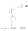
図1に、本発明の実施形態にかかる貼付位置画像検査装置の概略構成を示す。この貼付位置画像検査装置1は、液晶パネル上に駆動用ICを実装する際にACFの貼付位置を検査する装置である。ACFは回路基板同士又は回路基板とICその他の電子部品を導通状態で実装する際に使用される接着用フィルム状媒体であり、本例では液晶パネルにACFを貼り付けた後、その上に駆動用ICを熱圧着する場合を想定している。
【0022】
図1に示すように、貼付位置画像検査装置1は、CCDカメラ2と、レンズ3と、画像処理装置4を備える。レンズ3の下方にはワークとしての液晶パネル10が図示しない搬送装置により配置され、図中の矢印の方向へ順に搬送される。レンズ3は液晶パネル10上の所定領域の画像をCCDカメラ2により撮影可能とするために設けられる。よって、CCDカメラ2は液晶パネル10の、ACFが貼り付けられた部分の画像を撮影し、撮影画像を画像信号として画像処理装置4へ供給する。画像処理装置4は、CCDカメラ2から供給された画像信号に基づいて後述する判定処理を実行し、液晶パネル10の良/不良の判定、即ち液晶パネル10の所定の位置にACFが正しく貼り付けられているか否かの判定を行って、判定結果を出力する。
【0023】
図2はワークの一例としての液晶パネル10の平面図である。この液晶パネル10は、ガラスなどの一対の透明基板11及び12の間に図示しないシール材などを介して液晶が封入されてなる。下側の透明基板11は上側の透明基板12よりも面積が広く、上側の透明基板12よりも張り出した領域(以下、「張り出し領域」とも呼ぶ。)14を有する。この張り出し領域14上に駆動用ICがACF14を使用して貼り付けられる。なお、図2は図1に示す貼付位置画像検査装置1へ導入される状態の液晶パネル10、即ち張り出し領域14内にACF13が貼り付けられているが、駆動用ICは未だ実装されていない状態の液晶パネル10を示している。
【0024】
[検査方法]
次に、貼付位置画像検査装置による検査方法について説明する。この装置では、検査対象となる液晶パネル10の検査対象部分(ACFが貼り付けられた部分)の撮影画像を取得し、その撮影画像を予め用意した検査用パターン画像と重ねて画像処理を行う。
【0025】
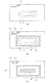
検査用パターン画像の一例を図3(c)に示す。検査用パターン画像30は、基本的に液晶パネル10の張り出し部14に対応するサイズの輪郭を有し、その内部に2つの位置合わせパターン31a及び31bと、貼付領域32と、非貼付領域33とを含む。
【0026】
位置合わせパターン31a及び31bは、液晶パネル10の撮影画像と検査用パターン画像30との位置合わせを行う際に使用されるパターンである。図1に示す貼付位置画像検査装置1において、ワークである液晶パネル10は図示しない搬送装置によりレンズ3の下方に配置され、その状態で液晶パネル10のACF貼付部分が撮影される。この際、液晶パネル10はレンズ3を通じたCCDカメラ2の視野に対して常に一定の向きで配置されるとは限らない。即ち、CCDカメラ2の視野に対して、液晶パネル10が斜め方向にずれた状態などで配置される場合がある。そこで、斜めに配置された液晶パネル10の撮影画像を検査用パターン画像30bに対して正しく相対配置するために、検査用パターン画像30中に位置合わせパターン31a及び31bが設けられる。
【0027】
位置合わせパターン31a及び31bは、検査対象となる液晶パネル10上の任意の特徴的なパターン部分とすることができる。即ち、検査対象となる液晶パネル10の撮影画像に対して、検査用パターン画像が正しく重ね合わせられたときに、撮影画像中に存在するパターン(液晶パネル10が本来有するパターン)と一致するように、位置合わせパターン31a及び31bが設定される。なお、位置合わせパターンが2つ設定されている理由は、ワークの回転方向のずれを補正可能とするためである。
【0028】
検査用パターン画像30中の貼付領域32は、その全面にACFが貼り付けられるべき領域である。よって、貼付領域32の全面にACFが存在していない場合は、その液晶パネル10は不良であると判定される。一方、非貼付領域33は、ACFが貼り付けられてはならない領域である。よって、非貼付領域33内に一部でもACFが貼り付けられている場合には、その液晶パネルは不良であると判定される。
【0029】
通常、貼付領域32は、駆動用ICが貼り付けられるべき領域と同一、又は多少の余裕をみて、それより若干広い領域に設定される。一方、非貼付領域33は、好適には駆動用ICが貼り付けられるべき領域の外周に設定される。図3(c)に示すように、貼付領域32の外側に非貼付領域33を設定した場合、ACFは貼付領域32全体をカバーし、かつ、非貼付領域33には重ならないように貼り付けられる必要がある。
【0030】
次に、検査用パターン画像の生成方法について図4を参照しつつ説明する。検査用パターン画像は、貼付位置画像検査装置1による検査工程、即ち、実際に検査対象物である液晶パネルの検査を実行する前に、予め生成して画像処理装置4内に記憶しておくべきものである。検査用パターン画像は、検査対象物であるワーク(本例では液晶パネル10)の良品サンプルを図1に示す貼付位置画像検査装置1により撮影し、撮影画像に対して図3(c)に示した位置合わせパターン31a及び31、貼付領域32及び非貼付領域33を設定することにより生成される。図3(a)に検査対象物である液晶パネル10の良品サンプルの撮影画像を示す。
【0031】
まず、液晶パネルの良品サンプルを図1に示すようにレンズ3の下方に配置し、CCDカメラ2により張り出し部分14を撮影して図3(a)に示す良品サンプルの撮影画像を得る(ステップS1)。なお、図3(a)に示す良品サンプルの撮影画像は、電極配線パターン18と、ACF16と、駆動用IC17とが含まれている。
【0032】
次に、良品サンプルの撮影画像上に作業者が検査用パターン画像の各要素を設定する(ステップS2)。このときの様子が図3(b)に示されている。即ち、図3(a)に示す良品サンプルの撮影画像上に、検査用パターン画像の各要素を順に上書きするように設定している最中の画像イメージを図3(b)に示している。
【0033】
具体的には、まず、良品サンプルの撮影画像中で特徴的なパターンを有する部分を探し、その部分に位置合わせパターン31a及び31bを決定する。図3(b)の例では、良品サンプルの撮影画像中の左上の電極配線パターンの一部をそれぞれ位置合わせパターン31a及び31bに設定している。次に、良品サンプルの撮影画像中の駆動用IC17の領域を基準として、それとほぼ同一の領域に貼付領域32を設定し、さらにその周りに非貼付領域33を設定する。こうして、良品サンプルの撮影画像を基準として検査用パターン画像が生成される。図3(a)に示す良品サンプルの撮影画像に対して生成された検査用パターン画像の例が図3(c)に示すものとなっている。こうして生成された検査用パターン画像は、画像処理装置4内に保存される(ステップS3)。
【0034】
次に、実際の貼付位置画像検査について図5を参照しつつ説明する。なお、この貼付位置画像検査は、先に述べた検査用パターン生成処理により得られた検査用パターンを利用して行う。
【0035】
まず、検査対象となる液晶パネル10をレンズ3の下方の所定位置に配置した状態で、液晶パネル10の撮影画像(以下、「検査対象撮影画像」と呼ぶ。)を取り込む(ステップS11)。次に、取り込んだ検査対象撮影画像に対して、図3(c)に示す検査用パターン画像を重ねる(ステップS12)。この際には、検査用パターン画像中の位置合わせパターン31a及び31bと、取り込んだ検査対象撮影画像中の同一部分のパターンとが重なるように両画像の位置を相対的に調整する。この位置合わせにより、液晶パネル10が搬送装置により斜めに配置され、取り込んだ検査対象撮影画像が斜め方向にずれていたりしても、その検査対象撮影画像と検査用パターン画像とを正しく重ね合わせることができる。
【0036】
こうして、両画像を正しく配置したら、画像処理装置4による画像処理によって、その液晶パネル10の良否判定を行う(ステップS13)。この良否判定は、貼付領域32と非貼付領域33の両方について個別に行われる。そして、貼付領域32内の全面にACFが貼り付けられており、かつ、非貼付領域33内にACFが貼り付けられていないと判定された場合にのみ、当該液晶パネル10が良品と判定される。
【0037】
貼付領域32及び非貼付領域33内の判定は、基本的に画素毎の濃度比較により行われる。例えば、貼付領域32の判定では、ACFが貼り付けられている状態の基準サンプルの濃度を予め測定などに基づいて決定しておき、それに所定のマージン(誤差分)を考慮して貼付領域の濃度閾値を決定する。例えば、

【0038】
そして、検査対象撮影画像中の貼付領域内の全画素について、その濃度を上記の貼付領域の濃度閾値と比較する。そして、濃度閾値を超える濃度を有する画素が所定数以上である場合に、その貼付領域全体にACFが貼り付けられていると判定する。なお、この際の所定数は、貼付領域内の全画素数から所定の誤差分を減算した値とすることができる。
【0039】
以上と同様に、非貼付領域についても判定を行う。非貼付領域についても、濃度閾値を予め設定し、非貼付領域内の画素の濃度を濃度閾値と比較することにより判定が行われる。但し、非貼付領域の濃度閾値は、ACFが貼り付けられていない状態の基準サンプルの濃度に所定のマージンを考慮して決定される。例えば、
【0040】
そして、非貼付領域内の全画素のうち、濃度閾値より小さい濃度を有する画素数を所定数と比較し、所定数より多い場合にその非貼付領域にはACFが貼り付けられていないと判定する。なお、ここでの所定数は、非貼付領域を構成する全画素数から所定の誤差分を減算した数とする。
【0041】
こうして、貼付領域32には全面にACFが貼り付けられている、かつ、非貼付領域33にはACFが貼り付けられていない、との判定がなされた場合に、当該液晶パネル10が良品と判定される。
【0042】
こうして、1つの液晶パネル10に対して良否判定が終了すると、次の液晶パネル10について同様の良否判定が行われる。そして、検査対象物全てについて良否判定が終了すると(ステップS14:Yes)、処理は終了する。
【0043】
[変形例]
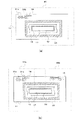
上記の例では、ACFの1つの貼付領域に対して1回で検査対象撮影画像を取り込むことができる場合を説明した。即ち、図6(a)に示すように、ACFの領域を、カメラ視野に基づいて決まる1つの検査範囲40でカバーできる場合を説明した。しかし、CCDカメラ2及びレンズ3により構成されるカメラ視野と検査対象物とのサイズの関係により、1回の撮影で検査対象物の検査領域を全て撮影できない場合もある。その場合には、例えば図6(b)に示すように、検査対象物の検査領域を複数に分割し、複数回の検査を繰り返すことにより1つの検査対象物の検査を行う。即ち、複数の検査範囲40a及び40bに分けて検査を行う。その際には、各検査範囲毎に上述の検査用パターン生成処理及び貼付位置画像検査処理を行うことになる。よって、各検査範囲毎に位置合わせパターンが設定されることになる。また、全ての検査範囲において良品と判定された検査対象物のみが良品となる。
【0044】
なお、複数の検査範囲を設定する際には、図6(b)の例に示すように、複数の検査範囲が重なるように設定することが望ましい。これは、検査範囲が重なるように設定することにより、検査範囲の境界部分で未検査領域が生じることを防止することができるからである。
【0045】
また、上記の説明では、液晶パネルに貼り付けたACFの貼付位置の検査に本発明を適用した例を示したが、ACF以外のフィルム状の媒体、例えばNCF(Non−Conductive Film)などの貼付位置検査にも本発明を適用することが可能である。
【0046】
また、上記の例では、検査用パターン画像中の位置合わせパターンを、良品サンプルの電極配線のパターンとしているが、これに限られることなく、良品サンプル上に存在する任意のパターン(例えば、電子部品、ワークの輪郭形状、ワークに設けられた穴など。但し、それらが撮影画像の濃度により特定できることが条件となる)を位置合わせパターンとして設定することが可能である。
【0047】
また、上記の例はワークとして液晶パネルを採り上げ、その張り出し領域にACFを貼り付けて駆動用ICを圧着する場合のものであるが、本発明はこれ以外の場合、例えばACFやNCFなどを使用したCOG(Chip On Glass)、COF(Chip On Film)、COB(Chip On Board)、TCP(Tape Carrier Package)などの場合についてももちろん適用が可能である。
【0048】
また、本発明は、基板と、該基板にフィルム状媒体を介して実装される電子部品と、を有してなる電子部品付き回路基板の製造装置又は製造方法に適用可能である。
【0049】
また、本発明は、電気光学装置と、該電気光学装置にフィルム状媒体を介して実装される電子部品、又は前記電気光学装置に接続される基板にフィルム状媒体を介して実装される電子部品と、を有してなる電気光学装置モジュールの製造装置又は製造方法に適用可能である。なお、電気光学装置に接続される基板としては、フレキシブル又はリジッドなものを用いることができる。
【0050】
尚、本発明の適用可能な電気光学装置としては、単純マトリクス方式あるいは、TFT(薄膜トランジスタ)やTFD(薄膜ダイオード)等のアクティブ素子(能動素子)を用いたアクティブマトリクス方式の液晶装置が挙げられる。
【0051】
さらに、本発明が適用可能な電気光学装置は、液晶装置に限定されず、エレクトロルミネッセンス装置、特に、有機エレクトロルミネッセンス装置、無機エレクトロルミネッセンス装置等や、プラズマディスプレイ装置、FED(フィールドエミッションディスプレイ)装置、LED(発光ダイオード)表示装置、電気泳動表示装置、薄型のブラウン管、液晶シャッター等を用いた小型テレビ、デジタルマイクロミラーデバイス(DMD)を用いた装置などの各種の電気光学装置が挙げられる。
【図面の簡単な説明】
【図1】本発明による貼付位置画像検査装置の概略構成を示す。
【図2】ワークの一例としての液晶パネルの構成を示す。
【図3】検査用パターン画像の例を示す。
【図4】検査用パターン画像生成処理のフローチャートである。
【図5】貼付位置画像検査処理のフローチャートである。
【図6】貼付位置画像検査処理の変形例を説明する図である。
【符号の説明】
1 貼付位置画像検査装置、 2 CCDカメラ、 3 レンズ、 4 画像処理装置、 10 液晶パネル(ワーク)、 13、16 ACF、 17 駆動用IC、 30 検査用パターン画像、 31a、31b 位置合わせパターン、 32 貼付領域、 33 非貼付領域[0001]
TECHNICAL FIELD OF THE INVENTION
The present invention relates to an image processing inspection for inspecting a position at which a film-like medium such as an anisotropic conductive film (Anisotropic Conductive Film) is attached to a work, an electro-optical device module manufacturing apparatus, an electro-optical device module manufacturing method, and an electronic device. The present invention relates to an apparatus for manufacturing a circuit board with components and a method for manufacturing a circuit board with electronic components.
[0002]
[Background Art]
An anisotropic conductive film (hereinafter, referred to as “ACF”) is used for mounting circuit boards on each other or between a circuit board and an electronic component. For example, when a driving IC is mounted on a liquid crystal panel or the like, an ACF is attached to a transparent substrate constituting the liquid crystal panel, and the driving IC is mounted thereon by thermocompression bonding. At this time, if the position where the ACF is stuck on the transparent substrate is not accurate, problems such as poor conduction between the electrode terminals formed on the transparent substrate and the terminals of the driving IC occur, and the liquid crystal panel is defective. It becomes. Therefore, in a state where the ACF is attached to the liquid crystal panel, an inspection is first performed to determine whether or not the attachment position is correct. An example of the ACF attaching device is described in
[0003]
Conventionally, as an inspection of the ACF attachment position, it is performed to determine the presence or absence of an ACF using image processing. For example, the presence or absence of the ACF is detected by measuring the reflectance using a photo sensor in the ACF attaching area, photographing the ACF attaching area by a CCD camera or the like, and performing image processing on the photographed image.
[0004]
[Patent Document 1]
JP-A-10-27820 [0005]
[Problems to be solved by the invention]
However, the above inspection is a level for detecting the presence or absence of the ACF, and is not a highly accurate detection. For example, even a small defect such as a partial missing of the ACF or a small missing portion such as a pinhole is detected. It could not be detected. Therefore, there is a problem that a work having the above-described defect is determined as a non-defective product.
[0006]
The present invention has been made in view of the above points, and it is an object of the present invention to provide an inspection apparatus and an inspection method capable of inspecting a bonding position of an adhesive material such as an ACF with high accuracy by image processing. I do.
[0007]
[Means for Solving the Problems]
According to one aspect of the present invention, in a sticking position image inspection device that inspects a sticking position of a film-like medium with respect to an inspection target, a plurality of alignment patterns corresponding to characteristic patterns existing on the inspection target and the film-like alignment pattern Means for acquiring a pattern image for inspection including a sticking area that is an area to which a medium is to be stuck, image acquiring means for acquiring a photographed image of the object to be inspected, and an image acquisition means for acquiring the inspection object using the alignment pattern. A photographing image, an image arranging means for relatively arranging the inspection pattern image, and, based on the photographed image of the inspection object in the attaching region, whether or not the sticking position of the film-shaped medium is appropriate. Determining means for determining whether
[0008]
The above-mentioned sticking position image inspection apparatus inspects the sticking position of a film-like medium such as an ACF stuck to an inspection object such as a liquid crystal panel by image processing. In the inspection, a captured image of the inspection object is acquired, and this is used with a previously prepared inspection pattern image. The inspection pattern image includes a plurality of alignment patterns corresponding to the characteristic patterns present on the inspection target and an attachment area to which the film-shaped medium is to be attached. The characteristic pattern present on the inspection object can be, for example, a wiring pattern formed on a substrate of a liquid crystal panel. Since the inspection pattern image includes such an alignment pattern and an attachment area to which the film-shaped medium is to be attached, the inspection pattern image is an image that maintains a relative positional relationship between the two. Then, in the inspection, using the alignment pattern, the photographed image of the inspection object and the inspection pattern image are relatively arranged, and whether or not the film-like medium is correctly attached in the attachment area is determined. Is determined by image processing. This makes it possible to perform image processing by correctly arranging the inspection pattern image on the image of the inspection object, and to inspect the sticking position with high accuracy.
[0009]
In one aspect of the pasting position image inspection apparatus, the determination unit includes a unit that compares a pixel density in a captured image of the inspection object in the pasting area with a predetermined first density value; Means for determining that the sticking position of the film-shaped medium is appropriate when there are a first predetermined number or more of pixels having a density value higher than the density value. In this aspect, the appropriateness of the sticking position is determined using the density of the pixels in the captured image of the inspection object.
[0010]
In one aspect of the above-described pasting position image inspection apparatus, the inspection pattern image includes a non-pasting area that is an area where the film-shaped medium should not be pasted, and the determination unit includes the non-pasting area in the non-pasting area. Means for comparing the pixel density in the captured image of the inspection object with a predetermined second density value; and a second predetermined number or more of pixels having a density lower than the second density value, and When there are at least a first predetermined number of pixels having a density higher than the first density value, it can be determined that the sticking position of the film-shaped medium is appropriate.
[0011]
In this embodiment, the inspection pattern image includes not only the sticking area but also a non-sticking area to which the film-like medium should not be attached. Therefore, by appropriately arranging the sticking area and the non-sticking area, it is possible to determine the suitability of the sticking position of the film medium with higher accuracy.
[0012]
Here, the first predetermined number can be a number obtained by subtracting a predetermined error from the total number of pixels included in the pasting area, and the second predetermined number is included in the non-pasting area. It can be a number obtained by subtracting a predetermined error from the total number of pixels.
[0013]
In one aspect of the pasting position image inspection apparatus, the image acquisition unit acquires a plurality of captured images from a region on the inspection target to which the film-shaped medium is attached, and the determination unit includes In the case where the sticking position of the film-shaped medium is appropriate for all of the photographed images, the sticking position can be determined to be appropriate. In this aspect, when the region where the film-shaped medium is pasted is large and one photographed image cannot cover the entire region, the acquisition and determination of photographed images are repeated for a plurality of regions, so that the entire pasting position is determined. Can be checked for suitability.
[0014]
According to another aspect of the present invention, in a sticking position image inspection method for inspecting a sticking position of a film-like medium with respect to an inspection object, a plurality of alignment patterns corresponding to characteristic patterns present on the inspection object and A step of obtaining a pattern image for inspection including a sticking area that is an area where the medium is to be stuck, and an image obtaining step of obtaining a captured image of the inspection target,
Using the alignment pattern, a photographed image of the inspection object, an image arrangement step of relatively arranging the inspection pattern image, and based on the photographed image of the inspection object in the attachment region, A determining step of determining whether or not the sticking position of the film-shaped medium is appropriate.
[0015]
According to the sticking position image processing method, the sticking position of the film-like medium can be inspected with high accuracy, similarly to the sticking position image processing apparatus.
[0016]
According to another aspect of the present invention, an electro-optical device and an electronic component mounted on the electro-optical device via a film medium, or mounted on a substrate connected to the electro-optical device via a film medium An apparatus for manufacturing an electro-optical device module including an electronic component can include the above-described sticking position image inspection device.
[0017]
According to another aspect of the present invention, an electro-optical device and an electronic component mounted on the electro-optical device via a film medium, or mounted on a substrate connected to the electro-optical device via the film medium The method for manufacturing an electro-optical device module including the electronic component to be used can use the above-described method for inspecting an attached position image.
[0018]
According to another aspect of the present invention, there is provided an apparatus for manufacturing a circuit board with electronic components, comprising: a substrate; and an electronic component mounted on the substrate via a film-like medium. An apparatus can be provided.
[0019]
Further, according to another aspect of the present invention, a method of manufacturing a circuit board with electronic components, comprising a substrate and an electronic component mounted on the substrate via a film-like medium, includes the above-described bonding position image inspection. A method can be used.
[0020]
BEST MODE FOR CARRYING OUT THE INVENTION
Hereinafter, preferred embodiments of the present invention will be described with reference to the drawings.
[0021]
[Configuration of sticking position image inspection device]
FIG. 1 shows a schematic configuration of a sticking position image inspection apparatus according to an embodiment of the present invention. The sticking position
[0022]
As shown in FIG. 1, the sticking position
[0023]
FIG. 2 is a plan view of the
[0024]
[Inspection methods]
Next, an inspection method using the sticking position image inspection apparatus will be described. In this apparatus, a captured image of a portion to be inspected (a portion to which an ACF is attached) of the
[0025]
FIG. 3C shows an example of the inspection pattern image. The
[0026]
The
[0027]
The
[0028]
The
[0029]
Normally, the sticking
[0030]
Next, a method of generating an inspection pattern image will be described with reference to FIG. The inspection pattern image should be generated in advance and stored in the image processing device 4 before the inspection process by the sticking position
[0031]
First, a non-defective sample of a liquid crystal panel is arranged below the
[0032]
Next, the operator sets each element of the inspection pattern image on the photographed image of the non-defective sample (step S2). The situation at this time is shown in FIG. That is, FIG. 3B shows an image image in which each element of the inspection pattern image is set to be sequentially overwritten on the photographed image of the non-defective sample shown in FIG.
[0033]
Specifically, first, a portion having a characteristic pattern is searched for in a captured image of a non-defective sample, and
[0034]
Next, the actual sticking position image inspection will be described with reference to FIG. The sticking position image inspection is performed using the inspection pattern obtained by the inspection pattern generation processing described above.
[0035]
First, in a state where the
[0036]
When both images are correctly arranged in this way, the quality of the
[0037]
The determination in the pasted
[0038]
Then, the density of all the pixels in the pasted area in the inspection target photographed image is compared with the density threshold of the pasted area. Then, when the number of pixels having a density exceeding the density threshold is equal to or more than a predetermined number, it is determined that the ACF is pasted on the entire pasting area. Note that the predetermined number at this time can be a value obtained by subtracting a predetermined error from the total number of pixels in the pasting area.
[0039]
In the same manner as above, the determination is also made for the non-pasted area. Also for the non-pasted area, the determination is made by setting a density threshold in advance and comparing the density of the pixels in the non-pasted area with the density threshold. However, the density threshold value of the non-pasted area is determined in consideration of a predetermined margin for the density of the reference sample to which the ACF is not pasted. For example,
[0040]
Then, among all the pixels in the non-pasting area, the number of pixels having a density smaller than the density threshold is compared with a predetermined number, and when it is larger than the predetermined number, it is determined that the ACF is not pasted in the non-pasting area. . Note that the predetermined number here is a number obtained by subtracting a predetermined error from the total number of pixels constituting the non-pasted area.
[0041]
In this way, when it is determined that the ACF is attached to the entire surface of the sticking
[0042]
When the pass / fail judgment is completed for one
[0043]
[Modification]
In the above example, a case has been described in which a captured image to be inspected can be captured once for one pasting region of the ACF. That is, as shown in FIG. 6A, the case where the ACF area can be covered by one
[0044]
When setting a plurality of inspection ranges, it is desirable to set the plurality of inspection ranges to overlap as shown in the example of FIG. This is because, by setting the inspection ranges to overlap with each other, it is possible to prevent an untested region from being generated at the boundary of the inspection range.
[0045]
Further, in the above description, an example in which the present invention is applied to the inspection of the attachment position of the ACF attached to the liquid crystal panel has been described. The present invention can be applied to position inspection.
[0046]
Further, in the above example, the alignment pattern in the inspection pattern image is a pattern of the electrode wiring of the non-defective sample, but is not limited to this, and may be any pattern (for example, an electronic component) existing on the non-defective sample. , The contour shape of the work, holes provided in the work, etc., provided that they can be specified by the density of the photographed image).
[0047]
In the above example, a liquid crystal panel is picked up as a work, and an ACF is attached to the overhanging area and a driving IC is crimped. However, the present invention uses other cases, such as using an ACF or NCF. Of course, the present invention can also be applied to the case of COG (Chip On Film), COF (Chip On Film), COB (Chip On Board), TCP (Tape Carrier Package), and the like.
[0048]
Further, the present invention is applicable to an apparatus or a method for manufacturing a circuit board with electronic components including a substrate and an electronic component mounted on the substrate via a film medium.
[0049]
Further, the present invention provides an electro-optical device and an electronic component mounted on the electro-optical device via a film medium, or an electronic component mounted on a substrate connected to the electro-optical device via a film medium. The present invention can be applied to a manufacturing apparatus or a manufacturing method of an electro-optical device module having: Note that a flexible or rigid substrate can be used as a substrate connected to the electro-optical device.
[0050]
The electro-optical device to which the present invention can be applied includes a simple matrix type or an active matrix type liquid crystal device using an active element (active element) such as a TFT (thin film transistor) or TFD (thin film diode).
[0051]
Further, the electro-optical device to which the present invention can be applied is not limited to a liquid crystal device, and may be an electroluminescent device, particularly, an organic electroluminescent device, an inorganic electroluminescent device, a plasma display device, an FED (field emission display) device, Various electro-optical devices such as an LED (light emitting diode) display device, an electrophoretic display device, a thin CRT, a small television using a liquid crystal shutter, and a device using a digital micromirror device (DMD) are exemplified.
[Brief description of the drawings]
FIG. 1 shows a schematic configuration of a sticking position image inspection apparatus according to the present invention.
FIG. 2 shows a configuration of a liquid crystal panel as an example of a work.
FIG. 3 shows an example of an inspection pattern image.
FIG. 4 is a flowchart of an inspection pattern image generation process.
FIG. 5 is a flowchart of a pasting position image inspection process.
FIG. 6 is a diagram illustrating a modification of the pasting position image inspection process.
[Explanation of symbols]
REFERENCE SIGNS
Claims (11)
検査対象物上に存在する特徴的パターンに対応する複数の位置合わせパターン及び前記フィルム状媒体が貼り付られるべき領域である貼付領域を含む検査用パターン画像を取得する手段と、
検査対象物の撮影画像を取得する画像取得手段と、
前記位置合わせパターンを利用して、前記検査対象物の撮影画像と、前記検査用パターン画像とを相対的に配置する画像配置手段と、
前記貼付領域内における前記検査対象物の撮影画像に基づいて、前記フィルム状媒体の貼付位置が適切であるか否かを判定する判定手段と、を備えることを特徴とする貼付位置画像検査装置。In a sticking position image inspection device that inspects the sticking position of the film-like medium with respect to the inspection target,
Means for obtaining a plurality of alignment patterns corresponding to the characteristic pattern present on the inspection object and an inspection pattern image including an attachment area that is an area to which the film-shaped medium is to be attached,
Image acquisition means for acquiring a captured image of the inspection object,
Using the alignment pattern, a photographed image of the inspection object, an image arrangement means for relatively arranging the inspection pattern image,
A sticking position image inspection apparatus, comprising: a determination unit that determines whether or not the sticking position of the film-like medium is appropriate based on a photographed image of the inspection target in the sticking area.
前記貼付領域内における前記検査対象物の撮影画像中の画素濃度を、所定の第1の濃度値と比較する手段と、
前記第1の濃度値より高い濃度を有する画素が第1の所定数以上存在する場合に、前記フィルム状媒体の貼付位置が適切であると判定する手段と、を備えることを特徴とする請求項2に記載の貼付位置画像検査装置。The determining means includes:
Means for comparing a pixel density in a captured image of the inspection object in the pasting area with a predetermined first density value;
Means for determining that the sticking position of the film-shaped medium is appropriate when there are a first predetermined number or more of pixels having a density higher than the first density value. 3. The sticking position image inspection apparatus according to 2.
前記判定手段は、
前記非貼付領域内における前記検査対象物の撮影画像中の画素濃度を、所定の第2の濃度値と比較する手段と、
前記第2の濃度値より低い濃度を有する画素が第2の所定数以上存在し、かつ、前記第1の濃度値より高い濃度を有する画素が第1の所定数以上存在する場合に、前記フィルム状媒体の貼付位置が適切であると判定することを特徴とする請求項2に記載の貼付位置画像検査装置。The inspection pattern image includes a non-stick area, which is an area where the film-like medium should not be stuck,
The determining means includes:
Means for comparing a pixel density in a photographed image of the inspection object in the non-sticking area with a predetermined second density value;
When a pixel having a density lower than the second density value is present in a second predetermined number or more and a pixel having a density higher than the first density value is present in a first predetermined number or more, the film The sticking position image inspection apparatus according to claim 2, wherein it is determined that the sticking position of the medium is appropriate.
前記判定手段は、前記複数の撮影画像全てについて前記フィルム状媒体の貼付位置が適切である場合に、前記貼り付け位置を適切であると判定することを特徴とする請求項1乃至5のいずれか一項に記載の貼付位置画像検査装置。The image obtaining means obtains a plurality of captured images from an area on the inspection target to which the film-shaped medium is attached,
6. The method according to claim 1, wherein the determining unit determines that the sticking position is appropriate when the sticking position of the film medium is appropriate for all of the plurality of captured images. The sticking position image inspection apparatus according to claim 1.
検査対象物上に存在する特徴的パターンに対応する複数の位置合わせパターン及び前記フィルム状媒体が貼り付られるべき領域である貼付領域を含む検査用パターン画像を取得する工程と、
検査対象物の撮影画像を取得する画像取得工程と、
前記位置合わせパターンを利用して前記検査対象物の撮影画像と、前記検査用パターン画像とを相対的に配置する画像配置工程と、
前記貼付領域内における前記検査対象物の撮影画像に基づいて、前記フィルム状媒体の貼付位置が適切であるか否かを判定する判定手工程と、を有することを特徴とする貼付位置画像検査方法。In a sticking position image inspection method for inspecting the sticking position of the film-like medium with respect to the inspection target,
A step of obtaining an inspection pattern image including a plurality of alignment patterns corresponding to the characteristic patterns present on the inspection object and an attachment area that is an area to which the film-shaped medium is to be attached,
An image acquisition step of acquiring a captured image of the inspection object,
Using the alignment pattern, a photographed image of the inspection object, an image arrangement step of relatively arranging the inspection pattern image,
A sticking position image inspection method, comprising: determining a sticking position of the film-shaped medium on the basis of a photographed image of the inspection object in the sticking region. .
請求項1乃至6のいずれか1項に記載の貼付位置画像検査装置を備えることを特徴とする電気光学装置モジュールの製造装置。An electro-optical device, and an electronic component mounted on the electro-optical device via a film medium, or an electronic component mounted on a substrate connected to the electro-optical device via a film medium. An electro-optical device module manufacturing apparatus comprising:
An apparatus for manufacturing an electro-optical device module, comprising the sticking position image inspection device according to any one of claims 1 to 6.
請求項7に記載の貼付位置画像検査方法を用いることを特徴とする電気光学装置モジュールの製造方法。An electro-optical device, and an electronic component mounted on the electro-optical device via a film medium, or an electronic component mounted on a substrate connected to the electro-optical device via a film medium. A method for manufacturing an electro-optical device module, comprising:
A method for manufacturing an electro-optical device module, comprising using the sticking position image inspection method according to claim 7.
請求項1乃至6のいずれか1項に記載の貼付位置画像検査装置を備えることを特徴とする電子部品付き回路基板の製造装置。A substrate, an electronic component mounted on the substrate via a film-like medium, and a device for manufacturing a circuit board with electronic components, comprising:
An apparatus for manufacturing a circuit board with electronic components, comprising the apparatus for inspecting an attached position image according to claim 1.
請求項7に記載の貼付位置画像検査方法を用いることを特徴とする電子部品付き回路基板の製造方法。A method for manufacturing a circuit board with electronic components, comprising: a substrate; and an electronic component mounted on the substrate via a film-like medium.
A method for manufacturing a circuit board with electronic components, comprising using the sticking position image inspection method according to claim 7.
Priority Applications (1)
| Application Number | Priority Date | Filing Date | Title |
|---|---|---|---|
| JP2003129009A JP2004334491A (en) | 2003-05-07 | 2003-05-07 | Adhesion position image inspection device, adhesion position image inspection method, manufacturing device of electro-optical device module, manufacturing method of electro-optical device module, manufacturing device of circuit board with electronic component, and manufacturing method of circuit board with electronic component |
Applications Claiming Priority (1)
| Application Number | Priority Date | Filing Date | Title |
|---|---|---|---|
| JP2003129009A JP2004334491A (en) | 2003-05-07 | 2003-05-07 | Adhesion position image inspection device, adhesion position image inspection method, manufacturing device of electro-optical device module, manufacturing method of electro-optical device module, manufacturing device of circuit board with electronic component, and manufacturing method of circuit board with electronic component |
Publications (1)
| Publication Number | Publication Date |
|---|---|
| JP2004334491A true JP2004334491A (en) | 2004-11-25 |
Family
ID=33504979
Family Applications (1)
| Application Number | Title | Priority Date | Filing Date |
|---|---|---|---|
| JP2003129009A Withdrawn JP2004334491A (en) | 2003-05-07 | 2003-05-07 | Adhesion position image inspection device, adhesion position image inspection method, manufacturing device of electro-optical device module, manufacturing method of electro-optical device module, manufacturing device of circuit board with electronic component, and manufacturing method of circuit board with electronic component |
Country Status (1)
| Country | Link |
|---|---|
| JP (1) | JP2004334491A (en) |
Cited By (4)
| Publication number | Priority date | Publication date | Assignee | Title |
|---|---|---|---|---|
| JP2007086276A (en) * | 2005-09-21 | 2007-04-05 | Seiko Epson Corp | Electrooptical device, electronic equipment, and method for manufacturing electrooptical device |
| JP2008071780A (en) * | 2006-09-12 | 2008-03-27 | Shibuya Kogyo Co Ltd | Method of detecting film pasting status |
| CN100406846C (en) * | 2006-03-20 | 2008-07-30 | 友达光电股份有限公司 | Alignment detection structure and alignment offset detection method |
| WO2018012192A1 (en) * | 2016-07-12 | 2018-01-18 | 吉野石膏株式会社 | Inspection method, inspection/notification method, manufacturing method including inspection method, inspection apparatus, and manufacturing apparatus |
-
2003
- 2003-05-07 JP JP2003129009A patent/JP2004334491A/en not_active Withdrawn
Cited By (7)
| Publication number | Priority date | Publication date | Assignee | Title |
|---|---|---|---|---|
| JP2007086276A (en) * | 2005-09-21 | 2007-04-05 | Seiko Epson Corp | Electrooptical device, electronic equipment, and method for manufacturing electrooptical device |
| CN100406846C (en) * | 2006-03-20 | 2008-07-30 | 友达光电股份有限公司 | Alignment detection structure and alignment offset detection method |
| JP2008071780A (en) * | 2006-09-12 | 2008-03-27 | Shibuya Kogyo Co Ltd | Method of detecting film pasting status |
| WO2018012192A1 (en) * | 2016-07-12 | 2018-01-18 | 吉野石膏株式会社 | Inspection method, inspection/notification method, manufacturing method including inspection method, inspection apparatus, and manufacturing apparatus |
| JPWO2018012192A1 (en) * | 2016-07-12 | 2019-04-25 | 吉野石膏株式会社 | Inspection method, inspection / notification method, manufacturing method including the inspection method, inspection apparatus and manufacturing apparatus |
| US10830707B2 (en) | 2016-07-12 | 2020-11-10 | Yoshino Gypsum Co., Ltd. | Inspection method, inspection and reporting method, manufacturing method including the inspection method, inspection apparatus, and manufacturing apparatus |
| JP6997457B2 (en) | 2016-07-12 | 2022-01-20 | 吉野石膏株式会社 | Inspection method, inspection / notification method, manufacturing method including the inspection method, inspection device and manufacturing device |
Similar Documents
| Publication | Publication Date | Title |
|---|---|---|
| JP2005191387A (en) | Method and device for testing image pickup element | |
| US7900348B2 (en) | Method of manufacturing an electronic component substrate | |
| JP2017181188A (en) | Circuit board inspection device | |
| TW201024724A (en) | Array test apparatus, and method of measuring position of point of substrate thereof and method of measuring coordinates of point photographed by camera assembly | |
| JP2004233184A (en) | Polarizing plate application accuracy inspection method of liquid crystal panel | |
| TWI678746B (en) | Semiconductor manufacturing device and method for manufacturing semiconductor device | |
| JP2021193744A (en) | Semiconductor manufacturing equipment and method for manufacturing semiconductor device | |
| JP2005122059A (en) | Inspection device | |
| JP2007013112A (en) | Device and method for substrate inspection | |
| JP2004334491A (en) | Adhesion position image inspection device, adhesion position image inspection method, manufacturing device of electro-optical device module, manufacturing method of electro-optical device module, manufacturing device of circuit board with electronic component, and manufacturing method of circuit board with electronic component | |
| JP2007212690A (en) | Inspection apparatus for liquid crystal panel and its inspection method | |
| TWI765517B (en) | Die bonding device and method of manufacturing semiconductor device | |
| JP2012042223A (en) | Acf attachment state inspection device or acf attachment and attachment state inspection device | |
| CN111725086B (en) | Semiconductor manufacturing apparatus and method for manufacturing semiconductor device | |
| TWI278054B (en) | Dispensing and inspecting apparatus and method thereof | |
| US11322059B2 (en) | Aging system and aging method of display device | |
| TWI381200B (en) | Alignment inspection method and apparatus | |
| US6961081B2 (en) | Positioning and inspecting system and method using same | |
| KR100643248B1 (en) | Method and apparatus for inspecting display panel | |
| TWI307769B (en) | Apparatus for inspecting leads and method thereof | |
| TWI752558B (en) | Die bonding device and manufacturing method of semiconductor device | |
| KR102563868B1 (en) | Apparatus for testing display device | |
| JP3700486B2 (en) | Contact type image sensor IC mounting position inspection method and contact type image sensor IC mounting position inspection apparatus | |
| KR100814047B1 (en) | Device bonding apparatus | |
| TW201137364A (en) | Method for testing a package structure |
Legal Events
| Date | Code | Title | Description |
|---|---|---|---|
| A621 | Written request for application examination |
Free format text: JAPANESE INTERMEDIATE CODE: A621 Effective date: 20060323 |
|
| RD04 | Notification of resignation of power of attorney |
Free format text: JAPANESE INTERMEDIATE CODE: A7424 Effective date: 20070403 |
|
| A761 | Written withdrawal of application |
Free format text: JAPANESE INTERMEDIATE CODE: A761 Effective date: 20080527 |