JP2004303876A - Alignment device of lens and laser chip in laser diode - Google Patents
Alignment device of lens and laser chip in laser diode Download PDFInfo
- Publication number
- JP2004303876A JP2004303876A JP2003093669A JP2003093669A JP2004303876A JP 2004303876 A JP2004303876 A JP 2004303876A JP 2003093669 A JP2003093669 A JP 2003093669A JP 2003093669 A JP2003093669 A JP 2003093669A JP 2004303876 A JP2004303876 A JP 2004303876A
- Authority
- JP
- Japan
- Prior art keywords
- lens
- laser chip
- center position
- light
- laser
- Prior art date
- Legal status (The legal status is an assumption and is not a legal conclusion. Google has not performed a legal analysis and makes no representation as to the accuracy of the status listed.)
- Pending
Links
Images


Abstract
Description
【0001】
【発明の属する技術分野】
本発明は、キャップに設けられているレンズの位置と、ステムに設けられ、光ビームを発生するレーザチップの位置とを相対的に合わせる位置合わせ装置に関するものである。
【0002】
【従来の技術】
図5は、従来の位置合わせ装置PS11を示すブロック図である。
【0003】
従来の位置合わせ装置PS11は、キャップCAに設けられているレンズL1の位置と、ステムSに設けられ、光ビームを発生するレーザチップ10の位置とを相対的に合わせる位置合わせ装置であり、プリズム20と、受光素子30と、移動手段70aと、画像処理装置92と、CRTモニタ93とを有する。
【0004】
そして、レンズL1の位置とレーザチップ10の位置とを合わせる場合、レーザチップ10を発光させ、この発光した光が、レンズL1を通過し、プリズム20で反射し、受光素子30で結像する。受光素子30で結像した像に基づいて、レーザチップ10の中心位置を、CRTモニタ93上で目視することができ、X−Y駆動モータ72を移動させながら、レーザチップ10の中心位置を、移動し、レンズL1の中心位置に、レーザチップ10の中心位置を合わせる。
【0005】
この場合、X−Yステージ71を手動で移動することによって、レンズL1の中心位置に、レーザチップ10の中心位置を合わせるようにしている。
【0006】
なお、高速大容量のデータ伝送が可能な光ファイバ通信に使用される光通信用レーザダイオード(基本的には、レーザチップ10と球レンズL1とによって構成されている)は、レーザ光を高効率で光ファイバに導入する必要があるので、レーザビームの光軸精度が要求される。
【0007】
レンズL1の中心位置に、レーザチップ10の中心位置を合わせる作業は、人手で実行し、自動化ができていない。
【0008】
【発明が解決しようとする課題】
したがって、上記従来例では、キャップに設けられているレンズの位置と、ステムに設けられ、光ビームを発生するレーザチップ10の位置とを相対的に合わせる位置合わせ装置において、レンズL1とレーザチップ10との相互位置を自動調整することができないという問題がある。
【0009】
本発明は、キャップに設けられているレンズの位置と、ステムに設けられ、光ビームを発生するレーザチップの位置とを相対的に合わせる位置合わせ装置において、レンズとレーザチップとの相互位置を自動調整することができる位置合わせ装置を提供することを目的とするものである。
【0010】
【課題を解決するための手段】
本発明は、キャップに設けられているレンズの位置と、ステムに設けられ、光ビームを発生するレーザチップの位置とを相対的に合わせる位置合わせ装置において、上記レーザチップからの光を反射させるプリズムと、上記プリズムで反射した上記レーザチップからの光を受光する受光素子と、上記プリズムと上記受光素子との間の第1の光軸上に設けられ、上記第1の光軸上の光を透過し、上記第1の光軸と直交する第2の光軸へ反射するハーフミラーと、上記第2の光軸上に設けられている光源と、上記光源からの光が上記ハーフミラー、上記プリズム、上記レンズ、上記プリズムの順で反射し、上記ハーフミラーを透過した光が上記受光素子で結像し、上記受光素子が出力した信号に基づいて、上記レンズの中心位置を求めるレンズ中心位置検出手段とを有することを特徴とするレーザダイオードにおけるレンズとレーザチップとの位置合わせ装置である。
【0011】
【発明の実施の形態および実施例】
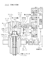
図1は、本発明の一実施例であるレーザダイオードにおけるレンズとレーザチップとの位置合わせ装置PS1を示す図である。
【0012】
位置合わせ装置PS1は、キャップCAに設けられているレンズL1の位置と、ステムSに設けられ、光ビームを発生するレーザチップ10の位置とを相対的に合わせる位置合わせ装置であり、プリズム20と、受光素子30と、ハーフミラー40と、光源50と、レンズ中心位置検出手段60と、移動手段70と、レンズ中心位置記憶手段M1と、レーザチップ中心位置検出手段80と、レーザチップ中心位置記憶手段M2と、位置合わせ制御手段90と、CRTモニタ91とを有する。
【0013】
図2は、上記実施例によって製造するレーザダイオードLDの断面を示す図である。
【0014】
レーザダイオードLDは、レーザチップ10と、レーザチップ10を固定しているステムSと、キャップCAと、キャップCAに保持されている球レンズL1と、リードLDとを有する。
【0015】
ここで、レーザチップ10は、ステムSに固定され、球レンズL1がキャップCAに固定されているので、レーザチップ10と球レンズL1とを位置合わせする場合、ステムSとキャップCAとを相対的に移動し、位置合わせする。
【0016】
プリズム20は、レーザチップ10からの光を反射させるプリズムである。
【0017】
受光素子30は、プリズム20で反射したレーザチップ10からの光を受光する受光素子であり、CCD等である。
【0018】
ハーフミラー40は、プリズム20と受光素子30との間の第1の軸A1と直交する第2の光軸A2上の光を反射するハーフミラーである。
【0019】
光源50は、第2の光軸A2上に設けられている光源である。
【0020】
レンズ中心位置検出手段60は、第1の光源50からの光がハーフミラー40、プリズム20、レンズL1、プリズム20で反射し、ハーフミラー40を透過した光が受光素子30で結像され、受光素子30が出力した信号に基づいて、レンズL1の中心位置を求める手段である。
【0021】
移動手段70は、キャップCAの位置と、ステムSの位置とを相対的に移動させる手段であり、X−Yステージ71と、X−Yステージ71を駆動するX−Y駆動モータ72と、モータコントローラ73とを有する。
【0022】
レンズ中心位置記憶手段M1は、レンズ中心位置検出手段60が検出したレンズ中心の位置を記憶するメモリである。
【0023】
レーザチップ中心位置検出手段80は、レーザチップ10が発光した光が、レンズL1を透過し、プリズム20で反射し、ハーフミラー40を透過した光が受光素子30で結像し、受光素子30が出力した信号に基づいて、レーザチップ10の中心位置を求める手段である。
【0024】
レーザチップ中心位置記憶手段M2は、レーザチップ中心位置検出手段80が検出したレーザチップ中心の位置を記憶するメモリである。
【0025】
位置合わせ制御手段90は、移動手段70によって、キャップCAの位置とステムSの位置とを相対的に移動させながら、レンズ中心位置とレーザチップ中心位置とを互いに合わせるように制御する手段である。
【0026】
図3は、上記実施例における位置合わせ過程で、レンズL1の反射光、レーザチップ10から受けた光がCRTモニタ91に表示されている例を示す図である。
【0027】
次に、上記実施例の動作について説明する。
【0028】
図4は、上記実施例の動作を示すフローチャートである。
【0029】
上記実施例において、図4(1)に示す粗調整が行なわれた後に、図4(2)に示す微調整が行われる。
【0030】
上記粗調整において、まず、光源50を点灯し、レンズL1の中心位置を求める(S1)。図1に示すように、光源50からの光が、光ファイバ51を介して、図中、下方から照射され、ハーフミラー40で反射し、プリズム20で反射し、レンズL1の表面で反射し、プリズム20で反射し、ハーフミラー40を通過した光が受光素子30で結像する。
【0031】
受光素子30の出力信号がレンズ中心位置検出手段60に送られ、画像処理され、レンズL1の中心位置が求められる。つまり、キャップCAに設けられているレンズL1に照射した光の反射光を画像処理し、レンズパターンを求め、この求めたレンズパターンに基づいて、レンズパターンの中心点を求め、レンズ中心位置とする。たとえば、上記レンズパターンの画像のうちで、最も輝度の高い位置を、レンズパターンの中心点の位置であるとして求める。
【0032】
図3に示すように、レンズL1で反射した光の中心の位置は、座標(x1,y1)として求められ、表示される。このようにして求められたレンズ中心位置は、レンズ中心位置記憶手段M1に格納される。
【0033】
なお、図3に示すCRTモニタ91における左上のコーナーの座標(x,y)を(0,0)とする。
【0034】
次に、光源50を消灯し(S2)、レーザチップ10を発光させ、レーザチップ10の中心位置を求める(S3)。図1に示すように、レーザチップ10で発生した光は、プリズム20で反射し、ハーフミラー40を通過し、受光素子30で結像する。受光素子30の出力信号がレーザチップ中心位置検出手段80に送られ、画像処理され、レーザチップ10の中心位置が求められる。
【0035】
つまり、レーザチップ10からの光の画像を画像処理し、レーザビームパターンを求め、この求めたレーザビームパターンに基づいて、レーザビームパターンの中心点を求め、レーザチップ10の中心位置とする。たとえば、上記レーザビームパターンの画像のうちで、最も輝度の高い位置を、レーザビームパターンの中心点の位置であるとして求める。
【0036】
図3に示すように、レーザチップ10から受けた光の中心位置は、座標(x2,y2)として求められ、表示される。このようにして求められたレーザチップ中心位置は、レーザチップ中心位置記憶手段M2に格納される。
【0037】
次に、レンズL1の中心位置(x1,y1)と、レーザチップ10の中心位置(x2,y2)との距離Lが、位置合わせ制御手段90で計算され(S4)、この計算された距離Lと、粗調整の基準であるたとえば30μmとを,位置合わせ制御手段90が比較し(S5)、距離Lが30μmよりも長ければ、位置合わせ制御手段90がモータ72を移動し(S6)、ステップS4に戻り、再び距離Lを求め、この求められた距離Lと基準の長さ30μmとが比較される。距離Lが30μm以下になれば(S5)、モータ72を駆動後、粗調整作業を終了する(S8)。
【0038】
上記粗調整が終了すると、次に、微調整作業に移る。図4(2)に示すように、格納済みのレンズL1の中心位置に対してレーザチップ10の中心位置を求める(S13)。
【0039】
次に、レンズL1の中心位置と、レーザチップ10の中心位置との距離Laが計算され(S14)、この計算された距離Laと、微調整の基準であるたとえば1μmとを比較し(S15)、距離Laが1μmよりも長ければ、モータ72を移動し(S16)、ステップS41に戻り、再び距離Laを求め、この求められた距離Laと1μmとを比較する。距離Laが1μm以下であれば(S15)、レーザチップ10を消灯し(S17)、微調整作業を終了する(S18)。
【0040】
上記実施例によれば、キャップCAに設けられているレンズL1の位置と、ステムSに設けられ、光ビームを発生するレーザチップ10の位置とを相対的に合わせる位置合わせ装置において、レンズL1とレーザチップ10との相互位置を自動調整することができる。
【0041】
なお,上記実施例において、上記レンズ中心位置と上記レーザチップ中心位置との距離が所定基準距離以下であれば、キャップCAとステムSとを固着する固着手段を有する。この場合、上記固着手段は、抵抗溶接手段であってもよい。なお、抵抗溶接する場合、上記レンズ中心と上記ビーム中心とを一致させ、その状態で上記溶接電極を相対的に接近させてキャップCAとステムSとを加圧し、溶接電流を流して溶接する。
【0042】
また、上記実施例において、上記レンズ中心位置と上記レーザチップ中心位置との距離が所定基準距離以下になると、上記レンズ中心位置と上記レーザチップ中心位置とを所定量、ずらす手段を有するようにしてもよい。
【0043】
上記のように、上記レンズ中心位置と上記レーザチップ中心位置とを所定量、ずらす場合、レンズL1とレーザチップ10とによって構成されるレーザダイオードLDに近接して設けられるファイバ(図示せず)の切断面の方向に、上記レンズ中心位置と上記レーザチップ中心位置とを調芯後、所定量、ずらす。このようにすることによって、上記ファイバへ光が入射するときにおける光の通過ロスが少なくなり、受光効率が向上し、つまり、ファイバの結合効率が向上する。
【0044】
上記ずらす所定量は、オフセット量としての意味が強く、ファイバの切断角度とレーザ光の入射角度とを調整することによって、レーザダイオードの特性に変化を持たせ、多品種のレーザをつくることができる。
【0045】
【発明の効果】
本発明によれば、キャップに設けられているレンズの位置と、ステムに設けられ、光ビームを発生するレーザチップの位置とを相対的に合わせる位置合わせ装置において、レンズとレーザチップとの相互位置を自動調整することができるという効果を奏する。
【図面の簡単な説明】
【図1】本発明の一実施例である位置合わせ装置PS1を示す図である。
【図2】上記実施例によって製造するレーザダイオードLDの断面を示す図である。
【図3】上記実施例における位置合わせ過程で、レンズL1の反射光、レーザチップ10から受けた光がCRTモニタ91に表示されている例を示す図である。
【図4】上記実施例の動作を示すフローチャートである。
【図5】従来の位置合わせ装置PS11を示すブロック図である。
【符号の説明】
PS1…位置合わせ装置、
L1…レンズ、
CA…キャップ、
S…ステム、
10…レーザチップ、
20…プリズム、
30…受光素子、
40…ハーフミラー、
50…光源、
51…光ファイバ、
60…レンズ中心位置検出手段、
M1…レンズ中心位置記憶手段、
70…移動手段、
71…X−Yステージ、
72…X−Y駆動モータ、
73…モータコントローラ、
74…可動コンタクタ、
80…レーザチップ中心位置検出手段、
M1…レーザチップ中心位置記憶手段、
90…位置合わせ制御手段、
91…CRTモニタ、
L、La…レンズL1の中心位置とレーザチップ10の中心位置との距離。[0001]
TECHNICAL FIELD OF THE INVENTION
The present invention relates to an alignment device that relatively aligns a position of a lens provided on a cap with a position of a laser chip provided on a stem and generating a light beam.
[0002]
[Prior art]
FIG. 5 is a block diagram showing a conventional positioning device PS11.
[0003]
The conventional positioning device PS11 is a positioning device that relatively aligns the position of the lens L1 provided on the cap CA with the position of the laser chip 10 that is provided on the stem S and generates a light beam. 20, a
[0004]
Then, when matching the position of the lens L1 with the position of the laser chip 10, the laser chip 10 emits light, and the emitted light passes through the lens L1, is reflected by the
[0005]
In this case, the center position of the laser chip 10 is adjusted to the center position of the lens L1 by manually moving the
[0006]
A laser diode for optical communication (basically constituted by the laser chip 10 and the spherical lens L1) used for optical fiber communication capable of high-speed and large-capacity data transmission converts laser light with high efficiency. It is necessary to introduce the laser beam into the optical fiber, so that the optical axis accuracy of the laser beam is required.
[0007]
The operation of aligning the center position of the laser chip 10 with the center position of the lens L1 is performed manually and cannot be automated.
[0008]
[Problems to be solved by the invention]
Therefore, in the above-described conventional example, in the positioning device that relatively aligns the position of the lens provided on the cap with the position of the laser chip 10 that is provided on the stem and generates a light beam, the lens L1 and the laser chip 10 There is a problem that the mutual position cannot be automatically adjusted.
[0009]
The present invention provides an alignment apparatus that relatively aligns the position of a lens provided on a cap with the position of a laser chip that is provided on a stem and generates a light beam. It is an object of the present invention to provide an alignment device that can be adjusted.
[0010]
[Means for Solving the Problems]
The present invention provides a positioning device that relatively aligns a position of a lens provided on a cap with a position of a laser chip that is provided on a stem and generates a light beam, and a prism that reflects light from the laser chip. A light receiving element that receives light from the laser chip reflected by the prism; and a light receiving element that is provided on a first optical axis between the prism and the light receiving element, and transmits light on the first optical axis. A half mirror that transmits and reflects to a second optical axis orthogonal to the first optical axis; a light source provided on the second optical axis; The light reflected by the prism, the lens, and the prism in this order, transmitted through the half mirror, forms an image on the light receiving element, and determines a center position of the lens based on a signal output by the light receiving element. A positioning device between the lens and the laser chip in the laser diode; and a position detecting means.
[0011]
Embodiments and Examples of the Invention
FIG. 1 is a diagram showing an alignment apparatus PS1 for a lens and a laser chip in a laser diode according to an embodiment of the present invention.
[0012]
The positioning device PS1 is a positioning device that relatively aligns the position of the lens L1 provided on the cap CA with the position of the laser chip 10 that is provided on the stem S and generates a light beam. ,
[0013]
FIG. 2 is a diagram showing a cross section of the laser diode LD manufactured according to the above embodiment.
[0014]
The laser diode LD has a laser chip 10, a stem S fixing the laser chip 10, a cap CA, a ball lens L1 held by the cap CA, and a lead LD.
[0015]
Here, since the laser chip 10 is fixed to the stem S and the ball lens L1 is fixed to the cap CA, when the laser chip 10 and the ball lens L1 are aligned, the stem S and the cap CA are relatively positioned. Go to and align.
[0016]
The
[0017]
The
[0018]
The half mirror 40 is a half mirror that reflects light on a second optical axis A2 orthogonal to the first axis A1 between the
[0019]
The light source 50 is a light source provided on the second optical axis A2.
[0020]
The lens center position detecting means 60 reflects the light from the first light source 50 on the half mirror 40, the
[0021]
The moving
[0022]
The lens center position storage unit M1 is a memory that stores the position of the lens center detected by the lens center position detection unit 60.
[0023]
The laser chip center position detecting means 80 detects that the light emitted by the laser chip 10 passes through the lens L1, is reflected by the
[0024]
The laser chip center position storage unit M2 is a memory that stores the position of the laser chip center detected by the laser chip center position detection unit 80.
[0025]
The
[0026]
FIG. 3 is a diagram showing an example in which the reflected light of the lens L1 and the light received from the laser chip 10 are displayed on the CRT monitor 91 during the alignment process in the above embodiment.
[0027]
Next, the operation of the above embodiment will be described.
[0028]
FIG. 4 is a flowchart showing the operation of the above embodiment.
[0029]
In the above embodiment, after the coarse adjustment shown in FIG. 4A is performed, the fine adjustment shown in FIG. 4B is performed.
[0030]
In the coarse adjustment, first, the light source 50 is turned on, and the center position of the lens L1 is obtained (S1). As shown in FIG. 1, light from a light source 50 is irradiated from below in the figure via an optical fiber 51, reflected by a half mirror 40, reflected by a
[0031]
The output signal of the
[0032]
As shown in FIG. 3, the position of the center of the light reflected by the lens L1 is obtained as coordinates (x1, y1) and displayed. The lens center position obtained in this way is stored in the lens center position storage means M1.
[0033]
The coordinates (x, y) of the upper left corner of the CRT monitor 91 shown in FIG. 3 are (0, 0).
[0034]
Next, the light source 50 is turned off (S2), the laser chip 10 emits light, and the center position of the laser chip 10 is obtained (S3). As shown in FIG. 1, light generated by the laser chip 10 is reflected by the
[0035]
That is, the image of the light from the laser chip 10 is subjected to image processing, a laser beam pattern is obtained, and a center point of the laser beam pattern is obtained based on the obtained laser beam pattern, and is set as the center position of the laser chip 10. For example, in the image of the laser beam pattern, the position with the highest luminance is obtained as the position of the center point of the laser beam pattern.
[0036]
As shown in FIG. 3, the center position of the light received from the laser chip 10 is obtained and displayed as coordinates (x2, y2). The laser chip center position obtained in this way is stored in the laser chip center position storage means M2.
[0037]
Next, the distance L between the center position (x1, y1) of the lens L1 and the center position (x2, y2) of the laser chip 10 is calculated by the positioning control means 90 (S4), and the calculated distance L And the reference for coarse adjustment, for example, 30 μm, is compared by the positioning control means 90 (S 5). If the distance L is longer than 30 μm, the positioning control means 90 moves the motor 72 (S 6). Returning to S4, the distance L is obtained again, and the obtained distance L is compared with a reference length of 30 μm. When the distance L becomes equal to or less than 30 μm (S5), the coarse adjustment operation is terminated after driving the motor 72 (S8).
[0038]
When the coarse adjustment is completed, the process proceeds to a fine adjustment operation. As shown in FIG. 4B, the center position of the laser chip 10 is determined with respect to the center position of the stored lens L1 (S13).
[0039]
Next, a distance La between the center position of the lens L1 and the center position of the laser chip 10 is calculated (S14), and the calculated distance La is compared with, for example, 1 μm which is a reference for fine adjustment (S15). If the distance La is longer than 1 .mu.m, the motor 72 is moved (S16), the process returns to step S41, the distance La is calculated again, and the calculated distance La is compared with 1 .mu.m. If the distance La is equal to or less than 1 μm (S15), the laser chip 10 is turned off (S17), and the fine adjustment operation is completed (S18).
[0040]
According to the above-described embodiment, in a positioning apparatus that relatively aligns the position of the lens L1 provided on the cap CA with the position of the laser chip 10 provided on the stem S and generating a light beam, The mutual position with the laser chip 10 can be automatically adjusted.
[0041]
In the above embodiment, if the distance between the center position of the lens and the center position of the laser chip is equal to or less than a predetermined reference distance, a fixing means for fixing the cap CA and the stem S is provided. In this case, the fixing means may be resistance welding means. In the case of resistance welding, the center of the lens and the center of the beam are made to coincide with each other, and in this state, the welding electrode is relatively approached to press the cap CA and the stem S, and welding is performed by supplying a welding current.
[0042]
Further, in the above embodiment, when the distance between the lens center position and the laser chip center position is equal to or less than a predetermined reference distance, a means for shifting the lens center position and the laser chip center position by a predetermined amount is provided. Is also good.
[0043]
As described above, when the center position of the lens and the center position of the laser chip are shifted by a predetermined amount, a fiber (not shown) provided close to the laser diode LD constituted by the lens L1 and the laser chip 10 is used. After centering the center position of the lens and the center position of the laser chip in the direction of the cut surface, the center position is shifted by a predetermined amount. By doing so, light passing loss when light enters the fiber is reduced, and light receiving efficiency is improved, that is, fiber coupling efficiency is improved.
[0044]
The predetermined amount to be shifted has a significant meaning as an offset amount, and by adjusting the fiber cutting angle and the incident angle of the laser beam, the characteristics of the laser diode can be changed to produce a wide variety of lasers. .
[0045]
【The invention's effect】
According to the present invention, in a positioning apparatus that relatively aligns a position of a lens provided on a cap with a position of a laser chip that is provided on a stem and generates a light beam, a mutual position of the lens and the laser chip is provided. Can be automatically adjusted.
[Brief description of the drawings]
FIG. 1 is a diagram showing a positioning device PS1 according to an embodiment of the present invention.
FIG. 2 is a diagram showing a cross section of a laser diode LD manufactured according to the embodiment.
FIG. 3 is a diagram showing an example in which light reflected by a lens L1 and light received from a laser chip 10 are displayed on a CRT monitor 91 in the alignment process in the embodiment.
FIG. 4 is a flowchart showing the operation of the embodiment.
FIG. 5 is a block diagram showing a conventional positioning device PS11.
[Explanation of symbols]
PS1: Positioning device,
L1 ... Lens,
CA… Cap,
S ... stem,
10 laser chip,
20 ... Prism,
30 ... light receiving element,
40 ... half mirror,
50 ... light source,
51 ... optical fiber,
60 ... lens center position detecting means,
M1: lens center position storage means,
70 ... Transportation means,
71 ... XY stage,
72 ... XY drive motor,
73 ... motor controller,
74 ... movable contactor,
80 ... Laser chip center position detecting means,
M1: laser chip center position storage means,
90 ... alignment control means,
91 ... CRT monitor,
L, La: distance between the center position of the lens L1 and the center position of the laser chip 10.
Claims (8)
上記レーザチップからの光を反射させるプリズムと;
上記プリズムで反射した上記レーザチップからの光を受光する受光素子と;
上記プリズムと上記受光素子との間の第1の光軸上に設けられ、上記第1の光軸上の光を透過し、上記第1の光軸と直交する第2の光軸へ反射するハーフミラーと;
上記第2の光軸上に設けられている光源と;
上記光源からの光が上記ハーフミラー、上記プリズム、上記レンズ、上記プリズムの順で反射し、上記ハーフミラーを透過した光が上記受光素子で結像し、上記受光素子が出力した信号に基づいて、上記レンズの中心位置を求めるレンズ中心位置検出手段と;
を有することを特徴とするレーザダイオードにおけるレンズとレーザチップとの位置合わせ装置。In a positioning device that relatively aligns the position of the lens provided on the cap with the position of the laser chip that is provided on the stem and generates a light beam,
A prism for reflecting light from the laser chip;
A light receiving element for receiving light from the laser chip reflected by the prism;
It is provided on a first optical axis between the prism and the light receiving element, transmits light on the first optical axis, and reflects light on a second optical axis orthogonal to the first optical axis. A half mirror;
A light source provided on the second optical axis;
The light from the light source is reflected in the order of the half mirror, the prism, the lens, and the prism, and the light transmitted through the half mirror forms an image on the light receiving element, based on a signal output from the light receiving element. Lens center position detecting means for obtaining the center position of the lens;
A positioning device for a lens and a laser chip in a laser diode, comprising:
上記キャップの位置と、上記ステムの位置とを相対的に移動させる移動手段を有することを特徴とするレーザダイオードにおけるレンズとレーザチップとの位置合わせ装置。In claim 1,
A positioning device for a lens and a laser chip in a laser diode, comprising a moving means for relatively moving the position of the cap and the position of the stem.
上記レンズ中心位置検出手段が検出したレンズ中心の位置を記憶するレンズ中心位置記憶手段を有することを特徴とするレーザダイオードにおけるレンズとレーザチップとの位置合わせ装置。In claim 1,
An apparatus for aligning a lens and a laser chip in a laser diode, comprising a lens center position storing means for storing the position of the lens center detected by the lens center position detecting means.
上記レンズ中心位置検出手段が検出したレンズ中心の位置を記憶するレンズ中心位置記憶手段と;
上記レーザチップが発光した光が、上記レンズを透過し、上記プリズムで反射し、上記ハーフミラーを透過し、上記受光素子で結像し、上記受光素子が出力した信号に基づいて、上記レーザチップの中心位置を求めるレーザチップ中心位置検出手段と;
上記レーザチップ中心位置検出手段が検出したレーザチップ中心の位置を記憶するレーザチップ中心位置記憶手段と;
上記移動手段によって、上記キャップの位置と上記ステムの位置とを相対的に移動させながら、上記レンズ中心位置と上記レーザチップ中心位置とを互いに合わせるように制御する位置合わせ制御手段と;
を有することを特徴とするレーザダイオードにおけるレンズとレーザチップとの位置合わせ装置。In claim 2,
Lens center position storage means for storing the position of the lens center detected by the lens center position detection means;
The light emitted by the laser chip is transmitted through the lens, reflected by the prism, transmitted through the half mirror, imaged by the light receiving element, and based on a signal output by the light receiving element, the laser chip Laser chip center position detecting means for obtaining the center position of the laser chip;
Laser chip center position storage means for storing the position of the laser chip center detected by the laser chip center position detection means;
Positioning control means for controlling the lens center position and the laser chip center position to be aligned with each other while relatively moving the position of the cap and the position of the stem by the moving means;
A positioning device for a lens and a laser chip in a laser diode, comprising:
上記制御手段が、上記レンズ中心位置と上記レーザチップ中心位置との距離が所定基準距離以下であれば、上記キャップと上記ステムとを固着する固着手段を有することを特徴とするレーザダイオードにおけるレンズとレーザチップとの位置合わせ装置。In claim 4,
The lens in a laser diode, wherein the control means has fixing means for fixing the cap and the stem if a distance between the lens center position and the laser chip center position is equal to or less than a predetermined reference distance. Alignment device with laser chip.
上記固着手段は、抵抗溶接手段であることを特徴とするレーザダイオードにおけるレンズとレーザチップとの位置合わせ装置。In claim 5,
The positioning device for a lens and a laser chip in a laser diode, wherein the fixing means is a resistance welding means.
上記レンズ中心位置と上記レーザチップ中心位置との距離が所定基準距離以下になると、上記レンズ中心位置と上記レーザチップ中心位置とを所定量、ずらす手段を有することを特徴とするレーザダイオードにおけるレンズとレーザチップとの位置合わせ装置。In claim 1,
When the distance between the lens center position and the laser chip center position is equal to or less than a predetermined reference distance, the lens in the laser diode having means for shifting the lens center position and the laser chip center position by a predetermined amount, Alignment device with laser chip.
上記レンズ中心位置と上記レーザチップ中心位置とを調芯後、所定量、ずらす場合、上記レンズと上記レーザチップとによって構成されるレーザダイオードに近接して設けられるファイバの切断面の方向に、上記レンズ中心位置と上記レーザチップ中心位置とを所定量、ずらすことを特徴とするレーザダイオードにおけるレンズとレーザチップとの位置合わせ装置。In claim 7,
When the center position of the lens and the center position of the laser chip are shifted by a predetermined amount after centering, in the direction of a cut surface of a fiber provided in close proximity to a laser diode formed by the lens and the laser chip, An apparatus for aligning a lens and a laser chip in a laser diode, wherein the center position of the lens and the center position of the laser chip are shifted by a predetermined amount.
Priority Applications (1)
| Application Number | Priority Date | Filing Date | Title |
|---|---|---|---|
| JP2003093669A JP2004303876A (en) | 2003-03-31 | 2003-03-31 | Alignment device of lens and laser chip in laser diode |
Applications Claiming Priority (1)
| Application Number | Priority Date | Filing Date | Title |
|---|---|---|---|
| JP2003093669A JP2004303876A (en) | 2003-03-31 | 2003-03-31 | Alignment device of lens and laser chip in laser diode |
Publications (1)
| Publication Number | Publication Date |
|---|---|
| JP2004303876A true JP2004303876A (en) | 2004-10-28 |
Family
ID=33406404
Family Applications (1)
| Application Number | Title | Priority Date | Filing Date |
|---|---|---|---|
| JP2003093669A Pending JP2004303876A (en) | 2003-03-31 | 2003-03-31 | Alignment device of lens and laser chip in laser diode |
Country Status (1)
| Country | Link |
|---|---|
| JP (1) | JP2004303876A (en) |
Cited By (2)
| Publication number | Priority date | Publication date | Assignee | Title |
|---|---|---|---|---|
| JP2015161909A (en) * | 2014-02-28 | 2015-09-07 | 株式会社村田製作所 | Optical transmission module and manufacturing method of optical transmission module |
| TWI566324B (en) * | 2012-03-26 | 2017-01-11 | 三菱電機股份有限公司 | Capping system |
-
2003
- 2003-03-31 JP JP2003093669A patent/JP2004303876A/en active Pending
Cited By (3)
| Publication number | Priority date | Publication date | Assignee | Title |
|---|---|---|---|---|
| TWI566324B (en) * | 2012-03-26 | 2017-01-11 | 三菱電機股份有限公司 | Capping system |
| JP2015161909A (en) * | 2014-02-28 | 2015-09-07 | 株式会社村田製作所 | Optical transmission module and manufacturing method of optical transmission module |
| US9470853B2 (en) | 2014-02-28 | 2016-10-18 | Murata Manufacturing Co., Ltd. | Optical transmission module and method of manufacturing optical transmission module |
Similar Documents
| Publication | Publication Date | Title |
|---|---|---|
| US7333255B2 (en) | Laser processing device | |
| JP3594706B2 (en) | Light source position adjustment device | |
| US20120133819A1 (en) | Automatic Focusing Apparatus and Method | |
| US8772688B2 (en) | Autofocus device including line image forming unit and rotation unit that rotates line image | |
| JP2008055455A (en) | Laser beam machining method and laser beam machining apparatus | |
| JP6056798B2 (en) | Edge detection device | |
| JP2007253167A (en) | Laser beam machining apparatus | |
| US10061109B2 (en) | Microscope system, method for controlling microscope system, and computer-readable recording medium | |
| JP2004303876A (en) | Alignment device of lens and laser chip in laser diode | |
| JP2857754B2 (en) | Auto-focusing device using double reflection | |
| JP2010120079A (en) | Microfabrication device and microfabrication method | |
| JP4681821B2 (en) | Laser focusing optical system and laser processing apparatus | |
| JP2001311866A (en) | Automatic focusing method and device for microscope | |
| JP2008310107A (en) | Focusing device and machining device equipped with the same | |
| JP2002023019A (en) | Assembling device for optical element module and optical axis control method | |
| JP2005106866A (en) | Focusing device for laser marking device | |
| JP2001050862A (en) | Measuring apparatus for aberration of optical-pickup objective lens | |
| JP2019163946A (en) | Noncontact surface profile measurement device | |
| JP2019155402A (en) | Centering method for laser beam and lase processing device | |
| JP2000312984A (en) | Laser device | |
| JP2005300478A (en) | Optical measuring apparatus | |
| JP2822698B2 (en) | Positioning device and laser processing device | |
| CN114755770B (en) | Automatic dimming system and dimming method for laser coupling optical fiber | |
| US11801570B2 (en) | Laser processing machine | |
| CN114623762B (en) | Method for three-dimensional registration alignment of double beams and multiple beams |
Legal Events
| Date | Code | Title | Description |
|---|---|---|---|
| A621 | Written request for application examination |
Free format text: JAPANESE INTERMEDIATE CODE: A621 Effective date: 20040825 |
|
| A977 | Report on retrieval |
Free format text: JAPANESE INTERMEDIATE CODE: A971007 Effective date: 20070622 |
|
| A131 | Notification of reasons for refusal |
Free format text: JAPANESE INTERMEDIATE CODE: A131 Effective date: 20070629 |
|
| A521 | Written amendment |
Free format text: JAPANESE INTERMEDIATE CODE: A523 Effective date: 20070824 |
|
| A02 | Decision of refusal |
Free format text: JAPANESE INTERMEDIATE CODE: A02 Effective date: 20071005 |