JP2004302113A - Antireflection film, optical member, optical system and projection exposure apparatus, and manufacturing method for antireflection film - Google Patents
Antireflection film, optical member, optical system and projection exposure apparatus, and manufacturing method for antireflection film Download PDFInfo
- Publication number
- JP2004302113A JP2004302113A JP2003094723A JP2003094723A JP2004302113A JP 2004302113 A JP2004302113 A JP 2004302113A JP 2003094723 A JP2003094723 A JP 2003094723A JP 2003094723 A JP2003094723 A JP 2003094723A JP 2004302113 A JP2004302113 A JP 2004302113A
- Authority
- JP
- Japan
- Prior art keywords
- refractive index
- antireflection film
- layer
- base material
- wavelength
- Prior art date
- Legal status (The legal status is an assumption and is not a legal conclusion. Google has not performed a legal analysis and makes no representation as to the accuracy of the status listed.)
- Pending
Links
Images


Abstract
Description
【0001】
【発明の属する技術分野】
本発明は、レンズ、プリズム、反射ミラー等の表面に積層される光学薄膜、この光学薄膜を備えた光学部材、この光学部材を備えた光学系及び投影露光装置、並びに前記光学薄膜を製造する方法に関する。
【0002】
【従来の技術】
従来、投影露光装置(ステッパー)では、多数のレンズが使用されており、結像系だけでも数十面のレンズ枚数が使用されている。このような装置では、レンズ等の光学部材の表面反射が大きいと、フレヤーゴーストが生じて結像性能が悪化したり、光源からウエハーまでに到達する光量が小さくなることから、露光効率が悪化する。例えば、一面当りの反射率が0.3%であると、光学部品の枚数が50枚(100面)の場合、1−(1−0.003)100より26%近い光量がロスすることになる。
【0003】
そのため、ステッパーの光学系においては、レンズ等の光学部材の表面反射による光量損失やフレアー・ゴースト等の低減等を目的に、光学部材の表面に反射防止膜が形成されている。従って、この光学部材に施される反射防止膜では、露光波長において0%反射に近いことが要求される。
【0004】
また、近年、半導体素子の集積度を増すために、ステッパーの高解像化の要求が高まっている。このステッパーによるフォトリソグラフィーの解像度を上げる一つの方法として、光源波長の短波長化が挙げられる。最近では、水銀ランプよりも短波長域の光を発振でき、かつ高出力なエキシマレーザーを光源としたステッパーの実用化が普及してきた。そのため、反射防止膜としても、そのような短波長の光を透過できる必要があり、該短波長の光を透過可能な限られた成膜材料により構成される必要がある。
【0005】
図1は、短波長の光を透過可能な従来の反射防止膜の例を示す模式図である。図において、10は基材14の表面に積層された反射防止膜であり、入射媒質側から基材10側までの層構成は、緻密に形成された低屈折率物質からなる第1層11、高屈折率物質からなる第2層12、低屈折率物質からなる第3層13からなっている。
【0006】
このような反射防止膜10の層構成の例を、表1に示す。ここでは、基材14は合成石英ガラスであり、設計中心波長λ0=193nmであり、入射媒質は空気である。
【0007】
【表1】

このような反射防止膜10のλ0=193nmにおける光線入射角度θ=0°の分光反射率特性を図29に示し、λ0=193nmにおける反射率角度特性を図30に示す。図30において、Rs、Rp、Raは、それぞれS偏光反射率、P偏光反射率、平均反射率((Rs+Rp)/2)を示している。
【0009】
図29の分光反射率特性図に示すように、この反射防止膜10の設計中心波長λ0=193nmにおいて、ほぼ0%の反射率となっている。
【0010】
しかし、曲率を持ったレンズ群から構成されるステッパーの光学系において、曲率を持ったレンズ全面に対して図29に示すような分光反射特性を得るためには、レンズの中心部、周辺部に関わらず、同じ膜厚で成膜される必要がある。ところが、一般に凸面形状を持ったレンズの場合、レンズ周辺に向かうにしたがって膜厚が薄くなっている。そのため、このような反射防止膜の場合、その分光特性が短波長にシフトし、露光波長で十分な反射防止効果を得ることができない。その結果、露光効率の低下およびフレアー・ゴースト等が生じるのみならず、レンズ中心部を通る光束とレンズ周辺部を通る光束との透過率差が大きくなるので、結像性能が悪くなっていた。
【0011】
また、このようなステッパーの光学系では、半導体の集積度を増すために、前記のような光源波長の短波長化とともに、光学系の開口数NAを大きくすることにより解像度を向上させることも行われている。
【0012】
ステッパー光学系に使用されるレンズ面への露光光の入射角度は、最大で約sin−1(NA)°であるため、NAの増大とともに露光光の入射角度が大きくなる。従って、レンズ表面に施される反射防止膜には、0°からsin−1(NA)°までの広い角度範囲において、より低い反射率であることが要求される。
【0013】
ところが、従来の反射防止膜では図30に示すように、入射角が大きくなると反射率は急激に増加し、角度特性が劣っていた。即ち、高入射角で光が入射するレンズ面において、高入射光の一部が反射してフレア・ゴーストを発生し、結像性能が低下するという問題があった。
【0014】
このような分光反射特性及び角度特性の問題は、反射防止膜の層数を多くすることにより改善できることが知られている。例えば、下記特許文献1では、表2に示すような6層構造の反射防止膜が提案されている。
【0015】
【表2】
ここでは、基材は合成石英ガラスであり、入射媒質は空気である。
【0017】
この6層構造の反射防止膜の分光反射防止特性を図31に、角度反射防止特性を図32に示す。
【0018】
この反射防止膜は設計中心波長193nmで185nm〜225nmの範囲でRa≦0.3%と広い分光反射防止帯域を持ち、角度反射防止性能についても0〜47°の角度範囲でRa≦0.5%という反射防止性能を有していた。
【0019】
【特許文献1】
特開2002−189101。
【0020】
【発明が解決しようとする課題】
しかしながら、表2に示されるような多層構造の従来の反射防止膜では、分光反射防止帯域については、レンズ周辺部での膜厚ずれに対して実用レベルの帯域の広さを有しているものの、角度反射防止特性については、未だ十分であるとはいえなかった。
【0021】
近年のステッパー投影光学系では、高解像度化のためにNA=0.8を超える光学系も検討されているが、その投影光学系での最大光線入射角は53°を超えるものとなる。そのため、従来の反射防止膜では到底十分な反射防止効果を得ることができないという問題点を有していた。
【0022】
しかも、反射防止膜の層数を多くして多数層を積層する従来の反射防止膜では、層数が多い分、製造に手間が掛かる上、反射防止膜と基材との膨張係数の差に起因して、成膜後の収縮量の差により生じる応力のため、光学部材に撓み等の歪みが生じやすいという問題点も有していた。
【0023】
そこで、本発明では、少ない積層数で、短波長の光における十分な分光特性及び角度特性を得ることが可能な反射防止膜を提供することを課題とし、更に、開口数NAを大きくして解像度を向上し易い光学部材、光学系、及び投影露光装置を提供することを課題とする。
【0024】
【課題を解決するための手段】
本発明は以上の課題を解決するため、反射防止膜の構成中に超低屈折率層を導入し、しかも超低屈折率層の配置を最適化することにより、従来の多層反射防止膜では実現し得ない、極めて優れた性能の反射防止膜を少ない層数により実現するに至った。
【0025】
即ち、請求項1に記載の反射防止膜は、基材上に積層された屈折率の異なる2つの層からなる反射防止膜であって、前記基材の屈折率をnsub、入射媒質側から前記基材側までの各層の屈折率をn1,n2、光学膜厚をd1,d2、λ0を設計中心波長としたとき、以下の条件を満たすことを特徴とする。
【0026】
【数9】
n1≦1.30、かつnsub=n1 1.50〜2.87<n2
d1=0.25λ0±21%
d2=0.50λ0±30%
また、請求項2に記載の反射防止膜は、基材上に積層された2つの層からなる反射防止膜であって、前記基材の屈折率をnsub、入射媒質側から前記基材側までの各層の屈折率をn1,n2、光学膜厚をd1,d2、λ0を設計中心波長としたとき、以下の条件を満たすことを特徴とする。
【0027】
【数10】
n1≦1.30、かつnsub=n2 1.10〜1.30=n1 1.80〜4.70
d1=0.25λ0±35%
d2=0.25λ0±60%
更に、請求項3に記載の反射防止膜は、基材上に積層された3つの層からなる反射防止膜であって、前記基材の屈折率をnsub、入射媒質側から前記基材側までの各層の屈折率をn1,n2,n3、膜厚をd1,d2,d3、λ0を設計中心波長としたとき、以下の条件を満たすことを特徴とする。
【0028】
【数11】
n1≦1.30、かつn3>n2>n1
d1=0.22λ0±25%
d2=0.08λ0+190%乃至−95%
d3=0.50λ0±27%
また、請求項4に記載の反射防止膜は、基材上に積層された3つの層からなる反射防止膜であって、前記基材の屈折率をnsub、入射媒質側から前記基材側までの各層の屈折率をn1,n2,n3、膜厚をd1,d2,d3、λ0を設計中心波長としたとき、以下の条件を満たすことを特徴とする。
【0029】
【数12】
n1≦1.30、かつn2>n3>n1
d1=0.29λ0±19%
d2=0.59λ0±11%
d3=0.10λ0+155%乃至−95%
更に、請求項5に記載の反射防止膜は、基材上に積層された4つの層からなる反射防止膜であって、前記基材の屈折率をnsub、入射媒質側から前記基材側までの各層の屈折率をn1,n2,n3,n4、膜厚をd1,d2,d3,d4、λ0を設計中心波長としたとき、以下の条件を満たすことを特徴とする。
【0030】
【数13】
n1≦1.30、かつn2=n4>n3>n1
d1=0.29λ0±21%
d2=0.18λ0±35%
d3=0.05λ0±85%
d4=0.27λ0±50%
また、請求項6に記載の反射防止膜は、基材上に積層された4つの層からなる反射防止膜であって、前記基材の屈折率をnsub、入射媒質側から前記基材側までの各層の屈折率をn1,n2,n3,n4、膜厚をd1,d2,d3,d4、λ0を設計中心波長としたとき、以下の条件を満たすことを特徴とする。
【0031】
【数14】
n1≦1.30、かつn2=n4>n3>n1
d1=0.32λ0±17%
d2=0.09λ0±51%
d3=0.62λ0±17%
d4=0.45λ0±31%
更に、請求項7に記載の反射防止膜は、基材上に積層された5つの層からなる反射防止膜であって、前記基材の屈折率をnsub、入射媒質側から前記基材側までの各層の屈折率をn1,n2,n3,n4,n5、膜厚をd1,d2,d3,d4,d5、λ0を設計中心波長としたとき、以下の条件を満たすことを特徴とする。
【0032】
【数15】
n1≦1.30、かつn2=n4>n3=n5>n1
d1=0.31λ0±17%
d2=0.22λ0±27%
d3=0.11λ0±29%
d4=0.16λ0±26%
d5=0.21λ0±75%
また、請求項8に記載の反射防止膜は、基材上に積層された6つの層からなる反射防止膜であって、前記基材の屈折率をnsub、入射媒質側から前記基材側までの各層の屈折率をn1,n2,n3,n4,n5,n6、膜厚をd1,d2,d3,d4,d5,d6、λ0を設計中心波長としたとき、以下の条件を満たすことを特徴とする。
【0033】
【数16】
n1≦1.30、かつn2=n4=n6>n3=n5>n1
d1=0.30λ0±20%
d2=0.25λ0±25%
d3=0.10λ0±32%
d4=0.11λ0±37%
d5=0.33λ0±32%
d6=0.55λ0±28%
更に、請求項9に記載の反射防止膜は、請求項1〜8何れか一つに記載の構成に加え、波長140nm〜370nmの紫外線用に用いられるものであることを特徴とする。
【0034】
また、請求項10に記載の反射防止膜は、請求項1乃至9の何れか一つに記載の構成に加え、前記入射媒質に接する層が、空間充填密度60%以下のMgF2よりなることを特徴とする。
【0035】
更に、請求項11に記載の反射防止膜は、請求項1乃至10の何れか一つに記載の構成に加え、前記基材が、石英または蛍石からなることを特徴とする。
【0036】
また、請求項12に記載の光学部材は、前記基材の少なくとも一方の面に請求項1乃至11の何れか一つに記載の反射防止膜が積層されていることを特徴とする。
【0037】
更に、請求項13に記載の光学系は、請求項12に記載の光学部材を備え、NA≧0.80(NAは開口数を示す)であることを特徴とする。
【0038】
また、請求項14に記載の投影露光装置は、紫外線を露光光としてマスクを照明する照明光学系と、前記マスクのパターン像を基材上に投影露光する投影光学系とを備えた装置であって、前記投影光学系に請求項13に記載の光学部材を備えたことを特徴とする。
【0039】
更に、請求項15に記載のデバイス製造方法は、請求項14に記載の投影露光装置を用いて前記マスクのパターン像を被露光基板上に転写する工程を有することを特徴とする。
【0040】
また、請求項16に記載の反射防止膜の製造方法は、請求項1乃至11の何れか一つに記載の反射防止膜の製造方法であって、前記入射媒質に接する層をゾルゲル法により形成することを特徴とする。
【0041】
【発明の実施の形態】
以下、この発明の実施の形態について説明する。
【0042】
まず、本発明の反射防止膜は、レンズ、プリズム、フィルターなどの光学部材の基材の表面に積層される薄膜である。
【0043】
ここで、基材は、光学ガラス等の基材材料を光学部材の形状に成形したものである。基材材料は特に限定されないが、対象光が短波長の紫外線の場合には、使用波長に対する吸収が少ないという理由で、合成石英ガラス、蛍石等を用いるのが好ましい。
【0044】
反射防止膜は、成膜材料を複数層積層して構成されており、屈折率の異なる複数の層を有している。また、光学部材が配置される周囲の気体等の入射媒質に接する第1層が屈折率n1=1.3以下の超低屈折率層となっている。
【0045】
一般に、反射防止膜は屈折率が異なる層を積層することにより構成され、入射媒質に接する第1層の屈折率が他の層より相対的に低く設定されているが、本発明では、特に、第1層を超低屈折率層とすることにより、他の層の屈折率との差を大きくするとともに、第1層の屈折率を従来より低下させることにより、角度特性を向上し易くしている。
【0046】
この反射防止膜の各層を構成する成膜材料は、一般に光学薄膜として使用される材料であるが、設計中心波長λ0が140nm〜370nmの紫外線のように短波長領域の場合、例えば、TiO2、NdF3、LaF3、GdF3、DyF3、Al2O3、PbF2、HfO2などの高屈折率材料、SiO2、MgF2、AlF3、NaF、LiF、CaF2、BaF2、SrF2、YF3、Na3AlF6、Na5Al3F14などの低屈折率材料を用いることができる。設計中心波長λ0がArFエキシマレーザより短波長の場合には、SiO2またはフッ化物を用いるのが好ましい。
【0047】
ここで、屈折率n1=1.3以下の超低屈折率層は、該屈折率を有する成膜材料により成膜してもよいが、上記のような成膜材料を多孔質に形成し、その空間充填密度を調整することにより屈折率を低下させたものであってもよい。
【0048】
その場合、第1層の成膜材料としては、短波長領域、特に、200nm以下の波長領域で吸収が少くて、後述するウエットプロセスにより調製し易いという理由で、SiO2、MgF2、CaF2、BaF2、SrF2、Na3AlF6、Na5Al3F14、AlF3等が好ましく、特に、空間充填密度60%以下のSiO2、MgF2 が好適である。
【0049】
一方、第1層より基材側の層は、屈折率1.3より大きい材料からなるものである。
【0050】
このような反射防止膜の各層は、真空蒸着法、スパッタリング法、イオンプレーティング法、およびCVD法等のドライプロセス、ゾルゲル法等のウェットプロセスから選ばれた何れか一つ以上の方法により成膜することができる。入射媒質と接する第1層を多孔質に形成する場合には、ゾルゲル法等のウエットプロセスを用いれば成膜を容易にすることができるため好ましい。
【0051】
ゾルゲル法を用いて第1層を形成するには、例えば、成膜材料の原料となる金属ハライド、金属オキシハライド、金属有機化合物等の出発原料を、水、アルコール、フッ酸等の溶媒に混合して成膜材料ゾルを作成し、このゾルを加熱等により熟成処理した後、スプレー法、スピンコート法、ディップコート法等により基材に塗布し、ゲル膜を基材に堆積させ、その後、加熱することにより形成すればよい。
【0052】
ここで、フッ化物からなる層をゾルゲル法で形成するには、金属塩のアルコール溶液にフッ酸を加えて成膜材料ゾルを作成すればよい。また、ゾルゲル法により多孔質の第1層の空間充填密度を調整するには、分散媒を変更したり、ゾルの熟成処理における温度や熟成時間等の熟成条件を変更すればよい。
【0053】
そして、本発明では、このような反射防止膜の層構成は、設計中心波長λ0の光において適切な干渉条件が得られるように特定されている。ここでは、前記のように屈折率n1=1.3以下の超低屈折率層を用い、超低屈折率層を入射媒質と接する第1層に配置して最適化するとともに、各層の屈折率及び光学膜厚並びに層数が設定されている。
【0054】
具体的には、入射媒質側から基材側までの順に第1層、第2層、第3層、・・・それぞれの屈折率をn1,n2,n3,・・・、膜厚をd1,d2,d3,・・・とし、基材の屈折率をnsubとしたとき、2層構造の反射防止膜では、nsub=n1 1.50〜2.87<n2並びにd1=0.25λ0±21%及びd2=0.50λ0±30%の範囲にすることにより、或いは、nsub=n2 1.10〜1.30=n1 1.80〜4.70並びにd1=0.25λ0±35%及びd2=0.25λ0±60%の範囲にすることにより構成する。ここで、0.25λ0±35%とは、0.25λ0の値の上下35%以内の範囲である。
【0055】
また、3層構造の反射防止膜では、n3>n2>n1とするとともに、d1=0.22λ0±25%、d2=0.08λ0+190%乃至−95%、及びd3=0.50λ0±27%の範囲にすることにより、或いは、n2>n3>n1とするとともにd1=0.29λ0±19%、d2=0.59λ0±11%、d3=0.10λ0+155%乃至−95%の範囲にすることにより構成する。ここで、0.08λ0+190%乃至−95%とは、0.08λ0の5%の値から0.08λ0の290%の値までの範囲である。
【0056】
更に、4層構造の反射防止膜では、n2=n4>n3>n1とするとともに、d1=0.29λ0±21%、d2=0.18λ0±35%、d3=0.05λ0±85%、及びd4=0.27λ0±50%の範囲にすることにより、或いは、n2=n4>n3>n1とするとともに、d1=0.32λ0±17%、d2=0.09λ0±51%、d3=0.62λ0±17%、及びd4=0.45λ0±31%の範囲とすることにより構成する。
【0057】
また、5層構造の反射防止膜では、n2=n4>n3=n5>n1 とするとともに、d1=0.31λ0±17%、d2=0.22λ0±27%、d3=0.11λ0±29%、d4=0.16λ0±26%、及びd5=0.21λ0±75%の範囲とすることにより構成する。
【0058】
更に、6層構造の反射防止膜では、n2=n4=n6>n3=n5>n1とするとともに、d1=0.30λ0±20%、d2=0.25λ0±25%、d3=0.10λ0±32%、d4=0.11λ0±37%、d5=0.33λ0±32%、及びd6=0.55λ0±28%の範囲とすることにより構成する。
【0059】
このような各層構造の屈折率の範囲及び組合せ、並びに光学膜厚は、それぞれ前記のような範囲であれば、残存反射率が、実用上、反射防止膜として使用可能な1%を超えない範囲に抑えることができる。
【0060】
この発明では、このような特定の層構成とすることにより、従来より少ない積層数で、短波長の光に対する十分な分光反射特性を得易くするとともに、短波長の光における角度特性を向上し易くしている。そのため、このような反射防止膜を備えた光学部材では、従来に比べて、開口数NAを大きくすることが可能となり、また、積層数が少ないため製造が容易であり、更に、基材と反射防止膜との膨張係数の差に起因して、製造後の収縮量の差により生じる応力を抑えて、光学部材の撓み等の歪みを抑制し易い。
【0061】
次に、このような反射防止膜を有する光学部材を備えた投影露光装置30について説明する。
【0062】
図2は、この投影露光装置の基本構造を示し、ウェハー上にマスクのパターンのイメージを投影するための、ステッパと呼ばれるような投影露光装置に特に応用される。
【0063】
この投影露光装置30は少なくとも、表面に感光剤を塗布した被露光基板Wを置くことのできるウェハーステージ31,露光光としての真空紫外光を照射し、被露光基板W上にマスクRのパターンを転写するための照明光学系32,照明光学系32に露光光を供給するための光源33,被露光基板W上にマスクRのパターンのイメージを投影するための投影光学系34とを含む。投影光学系34はマスクRが配された最初の表面P1(物体面)と、被露光基板Wの表面に一致させた二番目の表面P2(像面)との間に配置されている。
【0064】
ウェハーステージ31はステージ制御系35により位置が制御される。照明光学系32は、マスクRと被露光基板Wとの間の相対位置を調節するための、アライメント光学系36を含んでいる。マスクRはウェハーステージ31の表面に対して平行に動くことのできるマスクステージ37に配置されている。マスク交換系38は、マスクステージ37にセットされたマスクRを交換し運搬する。マスク交換系38はウェハーステージ31の表面に対してマスクステージ37を平行に動かすためのステージドライバーを含んでいる。投影光学系34は、スキャンタイプの露光装置に応用されるアライメント光学系を持っている。更に、光源33、ステージ制御系35、アライメント光学系36、マスク交換系38は主制御部39によって制御されている。
【0065】
この投影露光装置30では、前記のような反射防止膜を有するレンズ等の光学部材が、詳細な図示は省略されているが、投影光学系34に使用されている。即ち、投影光学系34において、光路に反射防止膜を有するレンズ等が多数配置されている。
【0066】
このような投影露光装置30では、光源33からの照射光によりマスクRのパターン像を被露光基板W上に転写される。そして、この被露光基板Wに各種の後処理を施すことにより、半導体デバイス等のデバイスが製造される。
【0067】
そして、この投影露光装置30及びその光学系に、前記のような反射防止膜を有する光学部材が配置されているので、開口数NAを0.8以上にすることが可能となり、解像度をより高くすることができる。
【0068】
【実施例】
以下、本発明の実施例について説明する。これら実施例は実例によって説明されているが、本発明はこれらに限定されるものではない。
【0069】
[実施例1]
実施例1は、請求項1に対応する例で、ArFエキシマレーザ光(波長193nm)に対する2層反射防止膜であり、設計中心波長λ0=193nmである。その膜構成を表3に示す。この反射防止膜は合成石英ガラス基材(193nmにて屈折率1.55)上に積層されている。入射媒質は空気である。
【0070】
第一層は波長193nmの光にて屈折率1.26、光学的膜厚0.250λ0を有するウエットプロセスにて形成した空間充填密度60%のMgF2からなる多孔質層であり、第二層は波長193nmの光にて屈折率1.69、光学的膜厚0.500λ0を有するドライプロセスにて形成したLaF3からなる緻密な層である。
【0071】
【表3】
最上層である第一層のウエットプロセスのMgF2の成膜は、フッ酸/酢酸マグネシウム法により行なった。酢酸マグネシウムのメタノール溶液及びフッ酸からゾル液を調製後、オルガノサーマル処理を行い加熱熟成し、この溶液を基材上にスピンコートを行い、大気中で150℃で加熱することにより成膜した。
【0073】
第2層のドライプロセスの薄膜は真空蒸着法により膜材料を載置したボートに通電し、抵抗加熱蒸着により成膜した。
【0074】
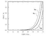
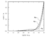
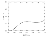
この反射防止膜の、190nm〜250nmの分光反射特性を図3に、波長193nmにおけるs偏光、p偏光、および平均に対する角度反射特性を図4に示す。
【0075】
図3及び図4より明らかなように、本発明の反射防止膜はわずか2層という少ない層数でありながら、190nm〜250nmの波長範囲でRa≦0.4%と広い分光反射防止帯域を有する。さらに、広い入射角範囲、すなわち0度(垂直入射)〜47度の範囲でs偏光およびp偏光および平均反射率が0.5%以下であり、従って偏光の違いによる反射率の差が極めて小さい。平均反射率は入射角50度を越えて53度においてもなお1.0%以下であり、角度反射防止特性においてもきわめて良好な反射防止性能を有していることがわかる。
【0076】
[実施例2]
実施例2は、請求項2に対応する例で、ArFエキシマレーザ光(波長193nm)に対する2層反射防止膜であり、設計中心波長λ0=193nmである。その膜構成を表4に示す。この反射防止膜は合成石英ガラス基材(193nmにて屈折率1.55)上に積層されている。入射媒質は空気である。
【0077】
第一層は波長193nmの光にて屈折率1.15、光学的膜厚0.250λ0を有するウエットプロセスにて形成した空間充填密度36%のMgF2から成り、第二層は波長193nmの光にて屈折率1.42、光学的膜厚0.250λ0を有するドライプロセスにて形成したMgF2から成る。この反射防止膜は最上層である第一層がウエットプロセスで形成される。ウエットプロセスのMgF2の成膜は、フッ酸/酢酸マグネシウム法により行なった。ゾル液を調製後、オルガノサーマル処理を行い加熱熟成し、この溶液を基材上にスピンコートを行い、大気中で150℃で加熱することにより形成され、ドライプロセスの薄膜は真空蒸着法により膜材料を乗せたボートに通電し、抵抗加熱蒸着により形成された。
【0078】
【表4】
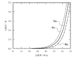
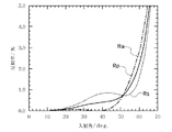
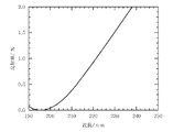
この反射防止膜の、190nm〜250nmの分光反射特性を図5に、波長193nmにおけるs偏光、p偏光、および平均に対する角度反射特性を図6に示す。
【0080】
図5及び図6より明らかなように、本発明の反射防止膜はわずか2層という少ない層数でありながら、190nm〜244nmの波長範囲でRa≦0.5%と広い分光反射防止帯域を有する。さらに、広い入射角範囲、すなわち0度(垂直入射)〜48度の範囲でs偏光およびp偏光および平均反射率が0.5%以下であり、従って偏光の違いによる反射率の差が極めて小さい。平均反射率は入射角50度を越えて57度においてもなお1.0%以下であり、角度反射防止特性においてもきわめて良好な反射防止性能を有していることがわかる。
【0081】
[比較例1]
比較例1として同じArFエキシマレーザ光(波長193nm)に対する2層反射防止膜を示した。その膜構成を表5に示す。この反射防止膜は合成石英ガラス基材(193nmにて屈折率1.55)上に積層されている。入射媒質は空気である。
【0082】
第一層は波長193nmの光にて屈折率1.42、光学的膜厚0.250λ0を有するドライプロセスのMgF2から成り、第二層は波長193nmの光にて屈折率1.69、光学的膜厚0.250λ0を有するドライプロセスのLaF3から成る。ここで設計中心波長λ0は設計膜厚の基準となる波長であり、ここでは193nmに選ばれた。この反射防止膜は2層全てがドライプロセスで形成された。ドライプロセスの薄膜は真空蒸着法により膜材料を乗せたボートに通電し、抵抗加熱蒸着により形成された。
【0083】
【表5】
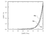
この反射防止膜の、190nm〜250nmの分光反射特性を図7に、s偏光、p偏光、および平均に対する、波長193nmにおける反射率の角度特性の測定結果を図8に示す。
【0085】
図7及び図8より明らかなように比較例1の反射防止膜は、Ra≦0.4%となる波長範囲は190nm〜210nmであり、分光反射防止帯域は狭いことがわかる。また、角度反射防止特性について見ると、入射角0度(垂直入射)においても反射率はおよそ0.2%と高く、さらに入射30度を超えるとs偏光とp偏光の反射率の差が無視できなくなるばかりか、平均反射率は33度以上で0.5%を超え、42度以上では1.0%を超えてしまった。
【0086】
このような反射防止膜を、光学系用のレンズ部品等の光学部材に適用すると、例えばN.A.が0.8以上の半導体露光用投影レンズの場合、この投影レンズに組み込まれたレンズ部品の各々には、入射角が約60度までの光が無視できない程度入射する。そのために、投影レンズは偏光の差による反射率の違いにより光学特性が変化してしまうという問題が生じるのみならず、反射損失による透過光量の減少、周辺光量の低下の問題が生じる。この問題は、構成レンズ部品の枚数が多い光学系ほど大きい。従って、このような光学系の場合、偏光を考慮して使用しなければならず、更に、このような考慮をしても、反射損失のために光学特性が充分でない。
【0087】
この問題は、投影レンズに限らず、組み込まれる光学部材に対する斜入射成分が大きい全ての光学系に生じる。
【0088】
以上の理由により、この反射防止膜を具えた光学部材を、N.A.≧0.8の投影レンズ、等の光学系に適用することは困難である。
【0089】
[実施例3]
実施例3は、請求項3に対応する例で、ArFエキシマレーザ光(波長193nm)に対する3層反射防止膜であり、設計中心波長λ0=193nmである。その膜構成を表6に示す。この反射防止膜は合成石英ガラス基材(193nmにて屈折率1.55)上に積層されている。入射媒質は空気である。
【0090】
第一層は波長193nmの光にて屈折率1.21、光学的膜厚0.214λ0を有するウエットプロセスにて形成した空間充填密度49%のMgF2から成り、第二層は波長193nmの光にて屈折率1.42、光学的膜厚0.114λ0を有するドライプロセスにて形成したMgF2から成り、第三層は波長193nmの光にて屈折率1.69、光学的膜厚0.489λ0を有するドライプロセスにて形成したLaF3から成る。
【0091】
この反射防止膜は最上層である第一層がウエットプロセスで形成される。ウエットプロセスのMgF2の成膜は、フッ酸/酢酸マグネシウム法により行なった。ゾル液を調製後、オルガノサーマル処理を行い加熱熟成し、この溶液を基材上にスピンコートを行い、大気中で150℃で加熱することにより形成され、ドライプロセスの薄膜は真空蒸着法により膜材料を乗せたボートに通電し、抵抗加熱蒸着により形成された。
【0092】
【表6】
この反射防止膜の、190nm〜250nmの分光反射特性を図9に、波長193nmにおけるs偏光、p偏光、および平均に対する角度反射特性を図10に示す。
【0094】
図9及び図10より明らかなように、本発明の反射防止膜は3層という少ない層数でありながら、190nm〜250nmの波長範囲でRa≦0.3%と広い分光反射防止帯域を有する。さらに、広い入射角範囲、すなわち0度(垂直入射)〜47度の範囲でs偏光およびp偏光および平均反射率が0.5%以下であり、従って偏光の違いによる反射率の差が極めて小さい。平均反射率は入射角55度においてもなお1.0%以下であり、角度反射防止特性においてもきわめて良好な反射防止性能を有していることがわかる。
【0095】
[実施例4]
実施例4は、請求項4に対応する例で、ArFエキシマレーザ光(波長193nm)に対する3層反射防止膜であり、設計中心波長λ0=193nmである。その膜構成を表7に示す。この反射防止膜は合成石英ガラス基材(193nmにて屈折率1.55)上に積層されてる。入射媒質は空気である。
【0096】
第一層は波長193nmの光にて屈折率1.21、光学的膜厚0.293λ0を有するウエットプロセスにて形成した空間充填密度49%のMgF2からなり、第二層は波長193nmの光にて屈折率1.69、光学的膜厚0.572λ0を有するドライプロセスにて形成したLaF3からなり、第三層は波長193nmの光にて屈折率1.42、光学的膜厚0.134λ0を有するドライプロセスにて形成したMgF2から成る。
【0097】
この反射防止膜は最上層である第一層がウエットプロセスで形成される。ウエットプロセスのMgF2の成膜は、フッ酸/酢酸マグネシウム法により行なった。ゾル液を調製後、オルガノサーマル処理を行い加熱熟成し、この溶液を基材上にスピンコートを行い、大気中で150℃で加熱することにより形成され、ドライプロセスの薄膜は真空蒸着法により膜材料を乗せたボートに通電し、抵抗加熱蒸着により形成された。
【0098】
【表7】
この反射防止膜の、190nm〜250nmの分光反射特性を図11に、波長193nmにおけるs偏光、p偏光、および平均に対する角度反射特性を図12に示す。
【0100】
図11及び図12より明らかなように、本発明の反射防止膜は3層という少ない層数でありながら、190nm〜240nmの波長範囲でRa≦0.5%と広い分光反射防止帯域を有する。さらに、広い入射角範囲、すなわち0度(垂直入射)〜55度の範囲でs偏光およびp偏光および平均反射率が0.5%以下であり、従って偏光の違いによる反射率の差が極めて小さい。平均反射率は入射角60度においてもなお1.0%以下であり、角度反射防止特性においてもきわめて良好な反射防止性能を有していることがわかる。
【0101】
[比較例2]
比較例2として、同じArFエキシマレーザ光(波長193nm)に対する3層反射防止膜を示した。設計中心波長λ0=193nmである。その膜構成を表8に示す。この反射防止膜は合成石英ガラス基材(193nmにて屈折率1.55)上に積層されている。入射媒質は空気である。
【0102】
第一層は波長193nmの光にて屈折率1.42、光学的膜厚0.262λ0を有するドライプロセスのMgF2から成り、第二層は波長193nmの光にて屈折率1.69、光学的膜厚0.266λ0を有するドライプロセスのLaF3から成り、第三層は波長193nmの光にて屈折率1.42、光学的膜厚0.605λ0を有するドライプロセスのMgF2から成る。ここで設計中心波長λ0は設計膜厚の基準となる波長であり、ここでは193nmに選ばれた。この反射防止膜は3層全てがドライプロセスで形成された。ドライプロセスの薄膜は真空蒸着法により膜材料を乗せたボートに通電し、抵抗加熱蒸着により形成された。
【0103】
【表8】
この反射防止膜の、190nm〜250nmの分光反射特性を図13に、s偏光、p偏光、および平均に対する、波長193nmにおける反射率の角度特性の測定結果を図14に示す。
【0105】
図13及び図14より明らかなように比較例2の反射防止膜は、Ra≦0.5%となる波長範囲は190nm〜212nmであり、分光反射防止帯域が狭いことがわかる。また、角度反射防止特性について見ると、入射角0度(垂直入射)での反射率は0%であるが、入射30度を超えるとs偏光とp偏光の反射率の差が無視できなくなるばかりか、平均反射率は0.5%を超え、43度以上では1.0%を超えてしまう。
【0106】
このような反射防止膜を、光学系用のレンズ部品等の光学部材に適用すると、例えばN.A.が0.8以上の半導体露光用投影レンズの場合、この投影レンズに組み込まれたレンズ部品の各々には、入射角が約60度までの光が無視できない程度入射する。そのために、投影レンズは偏光の差による反射率の違いにより光学特性が変化してしまうという問題が生じるのみならず、反射損失による透過光量の減少、周辺光量の低下の問題が生じる。この問題は、構成レンズ部品の枚数が多い光学系ほど大きい。従って、このような光学系の場合、偏光を考慮して使用しなければならず、更に、このような考慮をしても、反射損失のために光学特性が充分でない。
【0107】
この問題は、投影レンズに限らず、組み込まれる光学部材に対する斜入射成分が大きい全ての光学系に生じる。
【0108】
以上の理由により、この反射防止膜を具えた光学部材を、N.A.≧0.8の投影レンズ、等の光学系に適用することは困難である。
【0109】
[実施例5]
実施例5は、請求項5に対応した例で、ArFエキシマレーザ光(波長193nm)に対する4層反射防止膜であり、設計中心波長λ0=193nmである。その膜構成を表9に示す。この反射防止膜は合成石英ガラス基材(193nmにて屈折率1.55)上に積層されている。入射媒質は空気である。
【0110】
第一層は波長193nmの光にて屈折率1.21、光学的膜厚0.301λ0を有するウエットプロセスにて形成した空間充填密度49%のMgF2から成り、第二層は波長193nmの光にて屈折率1.69、光学的膜厚0.156λ0を有するドライプロセスにて形成したLaF3から成り、第三層は波長193nmの光にて屈折率1.42、光学的膜厚0.070λ0を有するドライプロセスにて形成したMgF2からなり、第四層は波長193nmの光にて屈折率1.69、光学的膜厚0.267λ0を有するドライプロセスにて形成したLaF3から成る。この反射防止膜は最上層である第一層がウエットプロセスで形成される。ウエットプロセスのMgF2の成膜は、フッ酸/酢酸マグネシウム法により行なった。ゾル液を調製後、オルガノサーマル処理を行い加熱熟成し、この溶液を基材上にスピンコートを行い、大気中で150℃で加熱することにより形成され、ドライプロセスの薄膜は真空蒸着法により膜材料を乗せたボートに通電し、抵抗加熱蒸着により形成された。
【0111】
【表9】
この反射防止膜の、190nm〜250nmの分光反射特性を図15に、波長193nmにおけるs偏光、p偏光、および平均に対する角度反射特性を図16に示す。
【0113】
図15及び図16より明らかなように、本発明の反射防止膜は4層という少ない層数でありながら、190nm〜250nmの波長範囲でRa≦0.2%と極めて広い分光反射防止帯域を有する。さらに、広い入射角範囲、すなわち0度(垂直入射)〜49度の範囲でs偏光およびp偏光および平均反射率が0.5%以下であり、従って偏光の違いによる反射率の差が極めて小さい。平均反射率は入射角50度を超えて57度においてもなお1.0%以下であり、角度反射防止特性においてもきわめて良好な反射防止性能を有していることがわかる。
【0114】
[実施例6]
実施例6は、請求項6に対応した例で、ArFエキシマレーザ光(波長193nm)に対する4層反射防止膜であり、設計中心波長λ0=193nmである。その膜構成を表10に示す。この反射防止膜は合成石英ガラス基材(193nmにて屈折率1.55)上に積層されている。入射媒質は空気である。
【0115】
第一層は波長193nmの光にて屈折率1.21、光学的膜厚0.315λ0を有するウエットプロセスにて形成した空間充填密度49%のMgF2から成り、第二層は波長193nmの光にて屈折率1.69、光学的膜厚0.072λ0を有するドライプロセスにて形成したLaF3から成り、第三層は波長193nmの光にて屈折率1.42、光学的膜厚0.641λ0を有するドライプロセスにて形成したMgF2から成り、第四層は波長193nmの光にて屈折率1.69、光学的膜厚0.461λ0を有するドライプロセスにて形成したLaF3から成る。
【0116】
この反射防止膜は最上層である第一層がウエットプロセスで形成される。ウエットプロセスのMgF2の成膜は、フッ酸/酢酸マグネシウム法により行なった。ゾル液を調製後、オルガノサーマル処理を行い加熱熟成し、この溶液を基材上にスピンコートを行い、大気中で150℃で加熱することにより形成され、ドライプロセスの薄膜は真空蒸着法により膜材料を乗せたボートに通電し、抵抗加熱蒸着により形成された。
【0117】
【表10】
この反射防止膜の、190nm〜250nmの分光反射特性を図17に、波長193nmにおけるs偏光、p偏光、および平均に対する角度反射特性を図18に示す。
【0119】
図17及び図18より明らかなように、本発明の反射防止膜は4層という少ない層数でありながら、190nm〜244nmの波長範囲でRa≦0.5%と広い分光反射防止帯域を有する。さらに、広い入射角範囲、すなわち0度(垂直入射)〜55度の範囲でs偏光およびp偏光および平均反射率が0.5%以下であり、従って偏光の違いによる反射率の差が極めて小さい。平均反射率は入射角60度を超えて61度においてもなお1.0%以下であり、角度反射防止特性においてもきわめて良好な反射防止性能を有していることがわかる。
【0120】
[比較例3]
比較例3として同じArFエキシマレーザ光(波長193nm)に対する4層反射防止膜を示した。設計中心波長λ0=193nmである。その膜構成を表11に示す。この反射防止膜は合成石英ガラス基材(193nmにて屈折率1.55)上に積層されている。入射媒質は空気である。
【0121】
第一層は波長193nmの光にて屈折率1.42、光学的膜厚0.272λ0を有するドライプロセスのMgF2から成り、第二層は波長193nmの光にて屈折率1.69、光学的膜厚0.269λ0を有するドライプロセスのLaF3から成り、第三層は波長193nmの光にて屈折率1.42、光学的膜厚0.641λ0を有するドライプロセスのMgF2から成り、第四層は波長193nmの光にて屈折率1.69、光学的膜厚0.068λ0を有するドライプロセスのLaF3から成る。ここで設計中心波長λ0は設計膜厚の基準となる波長であり、ここでは193nmに選ばれた。この反射防止膜は4層全てがドライプロセスで形成された。ドライプロセスの薄膜は真空蒸着法により膜材料を乗せたボートに通電し、抵抗加熱蒸着により形成された。
【0122】
【表11】
この反射防止膜の、190nm〜250nmの分光反射特性を図19に、s偏光、p偏光、および平均に対する、波長193nmにおける反射率の角度特性の測定結果を図20示す。
【0124】
図19及び図20より明らかなように比較例3の反射防止膜は、Ra≦0.5%となる波長範囲は190nm〜210nmであり、分光反射防止帯域が狭いことがわかる。また、角度反射防止特性について見ると、入射角0度(垂直入射)での反射率は0%であるが、入射角が35度を超えるとs偏光とp偏光の反射率の差が無視できなくなるばかりか、平均反射率は0.5%を超え、42度以上では1.0%を超えてしまう。このような反射防止膜を、光学系用のレンズ部品等の光学部材に適用すると、例えばN.A.が0.8以上の半導体露光用投影レンズの場合、この投影レンズに組み込まれたレンズ部品の各々には、一般に入射角が約60度までの光が無視できない程度入射する。そのために、投影レンズは偏光の差による反射率の違いにより光学特性が変化してしまうという問題が生じるのみならず、反射損失による透過光量の減少、周辺光量の低下の問題が生じる。この問題は、構成レンズ部品の枚数が多い光学系ほど大きい。従って、このような光学系の場合、偏光を考慮して使用しなければならず、更に、このような考慮をしても、反射損失のために光学特性が充分でない。
【0125】
この問題は、投影レンズに限らず、組み込まれる光学部材に対する斜入射成分が大きい全ての光学系に生じる。
【0126】
以上の理由により、この反射防止膜を具えた光学部材を、N.A.≧0.8の投影レンズ、等の光学系に適用することは困難である。
【0127】
[実施例7]
実施例7は、請求項7に対応した例で、ArFエキシマレーザ光(波長193nm)に対する5層反射防止膜であり、設計中心波長λ0=193nmである。その膜構成を表12に示す。この反射防止膜は合成石英ガラス基材(193nmにて屈折率1.55)上に積層されている。入射媒質は空気である。
【0128】
第一層は波長193nmの光にて屈折率1.21、光学的膜厚0.322λ0を有するウエットプロセスにて形成した空間充填密度49%のMgF2から成り、第二層は波長193nmの光にて屈折率1.69、光学的膜厚0.191λ0を有するドライプロセスにて形成したLaF3から成り、第三層は波長193nmの光にて屈折率1.42、光学的膜厚0.113λ0を有するドライプロセスにて形成したMgF2から成り、第四層は波長193nmの光にて屈折率1.69、光学的膜厚0.188λ0を有するドライプロセスにて形成したLaF3から成り、第五層は波長193nmの光にて屈折率1.42、光学的膜厚0.172λ0を有するドライプロセスにて形成したMgF2から成る。
【0129】
この反射防止膜は最上層である第一層がウエットプロセスで形成される。ウエットプロセスのMgF2の成膜は、フッ酸/酢酸マグネシウム法により行なった。ゾル液を調製後、オルガノサーマル処理を行い加熱熟成し、この溶液を基材上にスピンコートを行い、大気中で150℃で加熱することにより形成され、ドライプロセスの薄膜は真空蒸着法により膜材料を乗せたボートに通電し、抵抗加熱蒸着により形成された。
【0130】
【表12】
この反射防止膜の、190nm〜250nmの分光反射特性を図21に、波長193nmにおけるs偏光、p偏光、および平均に対する角度反射特性を図22に示す。
【0132】
図21及び図22より明らかなように、本発明の反射防止膜は5層という比較的少ない層数でありながら、190nm〜250nmの波長範囲でRa≦0.4%と広い分光反射防止帯域を有する。さらに、広い入射角範囲、すなわち0度(垂直入射)〜55度の範囲でs偏光およびp偏および平均反射率が0.5%以下であり、従って偏光の違いによる反射率の差が極めて小さい。平均反射率は入射角60度を超えて61度においてもなお1.0%以下であり、角度反射防止特性においてもきわめて良好な反射防止性能を有していることがわかる。
【0133】
[比較例4]
比較例4として同じArFエキシマレーザ光(波長193nm)に対する5層反射防止膜を示した。設計中心波長λ0=193nmである。その膜構成を表13に示す。この反射防止膜は合成石英ガラス基材(193nmにて屈折率1.55)上に積層されている。入射媒質は空気である。
【0134】
第一層は波長193nmの光にて屈折率1.42、光学的膜厚0.263λ0を有するドライプロセスのMgF2から成り、第二層は波長193nmの光にて屈折率1.69、光学的膜厚0.294λ0を有するドライプロセスのLaF3から成り、第三層は波長193nmの光にて屈折率1.42、光学的膜厚0.239λ0を有するドライプロセスのMgF2から成り、第四層は波長193nmの光にて屈折率1.69、光学的膜厚0.549λ0を有するドライプロセスのLaF3から成り、第五層は波長193nmの光にて屈折率1.42、光学的膜厚0.243λ0を有するドライプロセスのMgF2から成る。ここで設計中心波長λ0は設計膜厚の基準となる波長であり、ここでは193nmに選ばれた。この反射防止膜は5層全てがドライプロセスで形成された。ドライプロセスの薄膜は真空蒸着法により膜材料を乗せたボートに通電し、抵抗加熱蒸着により形成された。
【0135】
【表13】
この反射防止膜の、190nm〜250nmの分光反射特性を図23に、s偏光、p偏光、および平均に対する、波長193nmにおける反射率の角度特性の測定結果を図24に示す。
【0137】
図23及び図24より明らかなように比較例4の反射防止膜は、Ra≦0.5%となる波長範囲は190nm〜230nmであり、分光反射防止帯域が狭いことがわかる。また、角度反射防止特性について見ると、入射角0度(垂直入射)での反射率は0%であるが、入射角が30度を超えるとs偏光とp偏光の反射率の差が無視できなくなり、入射角が46度を超えると平均反射率は0.5%を超え、54度以上では1.0%を超えてしまう。このような反射防止膜を、光学系用のレンズ部品等の光学部材に適用すると、例えばN.A.が0.8以上の半導体露光用投影レンズの場合、この投影レンズに組み込まれたレンズ部品の各々には、一般に入射角が約60度までの光が無視できない程度入射する。そのために、投影レンズは偏光の差による反射率の違いにより光学特性が変化してしまうという問題が生じるのみならず、反射損失による透過光量の減少、周辺光量の低下の問題が生じる。この問題は、構成レンズ部品の枚数が多い光学系ほど大きい。従って、このような光学系の場合、偏光を考慮して使用しなければならず、更に、このような考慮をしても、反射損失のために光学特性が充分でない。
【0138】
この問題は、投影レンズに限らず、組み込まれる光学部材に対する斜入射成分が大きい全ての光学系に生じる。
【0139】
[実施例8]
実施例8は、請求項8に対応した例で、ArFエキシマレーザ光(波長193nm)に対する6層反射防止膜であり、設計中心波長λ0=193nmである。その膜構成を表14に示す。この反射防止膜は合成石英ガラス基材(193nmにて屈折率1.55)上に積層されている。入射媒質は空気である。
【0140】
第一層は波長193nmの光にて屈折率1.21、光学的膜厚0.308λ0を有するウエットプロセスにて形成した空間充填密度49%のMgF2から成り、第二層は波長193nmの光にて屈折率1.69、光学的膜厚0.201λ0を有するドライプロセスにて形成したLaF3から成り、第三層は波長193nmの光にて屈折率1.42、光学的膜厚0.129λ0を有するドライプロセスにて形成したMgF2から成り、第四層は波長193nmの光にて屈折率1.69、光学的膜厚0.120λ0を有するドライプロセスにて形成したLaF3から成り、第五層は波長193nmの光にて屈折率1.42、光学的膜厚0.309λ0を有するドライプロセスにて形成したMgF2から成り、第六層は波長193nmの光にて屈折率1.69、光学的膜厚0.542λ0を有するドライプロセスにて形成したLaF3から成る。
【0141】
この反射防止膜は最上層である第一層がウエットプロセスで形成される。ウエットプロセスのMgF2の成膜は、フッ酸/酢酸マグネシウム法により行なった。ゾル液を調製後、オルガノサーマル処理を行い加熱熟成し、この溶液を基材上にスピンコートを行い、大気中で150℃で加熱することにより形成され、ドライプロセスの薄膜は真空蒸着法により膜材料を乗せたボートに通電し、抵抗加熱蒸着により形成された。
【0142】
【表14】
この反射防止膜の、190nm〜250nmの分光反射特性を図25に、波長193nmにおけるs偏光、p偏光、および平均に対する角度反射特性を図26に示す。
【0144】
図25及び図26より明らかなように、本発明の反射防止膜は6層という比較的少ない層数でありながら、190nm〜244nmの波長範囲でRa≦0.5%と広い分光反射防止帯域を有する。さらに、広い入射角範囲、すなわち0度(垂直入射)〜54度の範囲でs偏光およびp偏および平均反射率が0.5%以下であり、従って偏光の違いによる反射率の差が極めて小さい。平均反射率は入射角60度を超えて61度においてもなお1.0%以下であり、角度反射防止特性においてもきわめて良好な反射防止性能を有していることがわかる。
【0145】
[比較例5]
比較例5として同じArFエキシマレーザ光(波長193nm)に対する6層反射防止膜を示した。設計中心波長λ0=193nmである。その膜構成を表15に示す。この反射防止膜は合成石英ガラス基材(193nmにて屈折率1.55)上に積層される。入射媒質は空気である。
【0146】
第一層は波長193nmの光にて屈折率1.42、光学的膜厚0.265λ0を有するドライプロセスのMgF2から成り、第二層は波長193nmの光にて屈折率1.69、光学的膜厚0.273λ0を有するドライプロセスのLaF3から成り、第三層は波長193nmの光にて屈折率1.42、光学的膜厚0.321λ0を有するドライプロセスのMgF2から成り、第四層は波長193nmの光にて屈折率1.69、光学的膜厚0.102λ0を有するドライプロセスのLaF3から成り、第五層は波長193nmの光にて屈折率1.42、光学的膜厚0.096λ0を有するドライプロセスのMgF2から成り、第六層は波長193nmの光にて屈折率1.69、光学的膜厚0.273λ0を有するドライプロセスのLaF3から成る。ここで設計中心波長λ0は設計膜厚の基準となる波長であり、ここでは193nmに選ばれた。この反射防止膜は6層全てがドライプロセスで形成された。ドライプロセスの薄膜は真空蒸着法により膜材料を乗せたボートに通電し、抵抗加熱蒸着により形成された。
【0147】
【表15】
この反射防止膜の、190nm〜250nmの分光反射特性を図27に、s偏光、p偏光、および平均に対する、波長193nmにおける反射率の角度特性の測定結果を図28に示す。
【0149】
図27及び図28より明らかなように比較例5の反射防止膜は、Ra≦0.5%となる波長範囲は190nm〜237nmであり、層数が増えた分だけ比較例1〜4よりも分光反射防止帯域は広くなっているものの実施例8にはおよばない。また、角度反射防止特性について見ると、入射角0度(垂直入射)での反射率は0%であるが、入射角が33度を超えるとs偏光とp偏光の反射率の差が無視できなくなり、入射角が42度を超えると平均反射率は0.5%を超え、50度以上では1.0%を超えてしまう。このような反射防止膜を、光学系用のレンズ部品等の光学部材に適用すると、例えばN.A.が0.8以上の半導体露光用投影レンズの場合、この投影レンズに組み込まれたレンズ部品の各々には、一般に入射角が約60度までの光が無視できない程度入射する。そのために、投影レンズは偏光の差による反射率の違いにより光学特性が変化してしまうという問題が生じるのみならず、反射損失による透過光量の減少、周辺光量の低下の問題が生じる。この問題は、構成レンズ部品の枚数が多い光学系ほど大きい。従って、このような光学系の場合、偏光を考慮して使用しなければならず、更に、このような考慮をしても、反射損失のために光学特性が充分でない。
【0150】
この問題は、投影レンズに限らず、組み込まれる光学部材に対する斜入射成分が大きい全ての光学系に生じる。
【0151】
以上の理由により、この反射防止膜を具えた光学部材を、N.A.≧0.8の投影レンズ、等の光学系に適用することは困難である。
【0152】
従って、実施例1〜8の反射防止膜は、比較例1〜5に比べ、300nm以下の紫外域で使用が可能で、層の総数が少なく、低い反射率特性、広い角度特性、少ない偏光特性の差を有する。そのため、これらの多層光学薄膜の少なくとも一つを投影レンズ、等の光学系に適用すれば、従来技術では実現が極めて困難であったN.A.≧0.8の高い光学性能の光学系が得られ、更にこの光学系を半導体露光装置、等の光学装置に用いれば高性能な光学装置が得られる。
【0153】
【発明の効果】
以上詳述の通り、請求項1乃至11に記載の発明によれば、複数の層からなる反射防止膜において、入射媒質側の第1層の透過率を1.30以下とするとともに、各層の屈折率及び光学膜厚を特定の構成にしたので、少ない積層数で、短波長の光における十分な分光反射特性及び角度特性を得ることが可能な反射防止膜を提供することができる。
【0154】
また、請求項12乃至16に記載の発明によれば、光学部材に分光反射特性及び角度特性に優れた反射防止膜を有する光学部材を備えているので、開口数NAを0.8以上に大きくすることにより解像度をより向上し易い光学部材、光学系、及び投影露光装置を提供することができる。
【図面の簡単な説明】
【図1】この発明及び従来の反射防止膜の構成を示す模式図である。
【図2】この発明の実施の形態の投影露光装置の基本構成を示す構成図である。
【図3】実施例1の結果を示すグラフであり、分光反射特性を示す。
【図4】実施例1の結果を示すグラフであり、角度反射特性を示す。
【図5】実施例2の結果を示すグラフであり、分光反射特性を示す。
【図6】実施例2の結果を示すグラフであり、角度反射特性を示す。
【図7】比較例1の結果を示すグラフであり、分光反射特性を示す。
【図8】比較例1の結果を示すグラフであり、角度反射特性を示す。
【図9】実施例3の結果を示すグラフであり、分光反射特性を示す。
【図10】実施例3の結果を示すグラフであり、角度反射特性を示す。
【図11】実施例4の結果を示すグラフであり、分光反射特性を示す。
【図12】実施例4の結果を示すグラフであり、角度反射特性を示す。
【図13】比較例2の結果を示すグラフであり、分光反射特性を示す。
【図14】比較例2の結果を示すグラフであり、角度反射特性を示す。
【図15】実施例5の結果を示すグラフであり、分光反射特性を示す。
【図16】実施例5の結果を示すグラフであり、角度反射特性を示す。
【図17】比較例3の結果を示すグラフであり、分光反射特性を示す。
【図18】比較例3の結果を示すグラフであり、角度反射特性を示す。
【図19】実施例6の結果を示すグラフであり、分光反射特性を示す。
【図20】実施例6の結果を示すグラフであり、角度反射特性を示す。
【図21】比較例4の結果を示すグラフであり、分光反射特性を示す。
【図22】比較例4の結果を示すグラフであり、角度反射特性を示す。
【図23】実施例7の結果を示すグラフであり、分光反射特性を示す。
【図24】実施例7の結果を示すグラフであり、角度反射特性を示す。
【図25】比較例5の結果を示すグラフであり、分光反射特性を示す。
【図26】比較例5の結果を示すグラフであり、角度反射特性を示す。
【図27】実施例8の結果を示すグラフであり、分光反射特性を示す。
【図28】実施例8の結果を示すグラフであり、角度反射特性を示す。
【図29】従来の3層構造の反射防止膜の分光反射特性を示グラフである。
【図30】従来の3層構造の反射防止膜の角度反射特性を示すグラフである。
【図31】従来の6層構造の反射防止膜の分光反射特性を示グラフである。
【図32】従来の6層構造の反射防止膜の角度反射特性を示すグラフである。
【符号の説明】
11 第1層
12 第2層
13 第3層
14 基材
30 投影露光装置[0001]
TECHNICAL FIELD OF THE INVENTION
The present invention relates to an optical thin film laminated on a surface of a lens, a prism, a reflection mirror, or the like, an optical member including the optical thin film, an optical system and a projection exposure apparatus including the optical member, and a method of manufacturing the optical thin film. About.
[0002]
[Prior art]
2. Description of the Related Art Conventionally, a projection exposure apparatus (stepper) uses a large number of lenses, and an imaging system alone uses several tens of lenses. In such an apparatus, when the surface reflection of an optical member such as a lens is large, a flare ghost occurs and the imaging performance deteriorates, or the light amount reaching the wafer from the light source decreases, so that the exposure efficiency deteriorates. . For example, if the reflectance per surface is 0.3%, and if the number of optical components is 50 (100 surfaces), 1- (1-0.003)100A light amount closer to 26% is lost.
[0003]
For this reason, in the optical system of the stepper, an antireflection film is formed on the surface of the optical member for the purpose of reducing light loss, flare, ghost, and the like due to surface reflection of the optical member such as a lens. Therefore, the antireflection film applied to this optical member is required to be close to 0% reflection at the exposure wavelength.
[0004]
In recent years, in order to increase the degree of integration of semiconductor elements, there is an increasing demand for higher resolution steppers. One method of increasing the resolution of photolithography using this stepper is to shorten the wavelength of the light source. Recently, practical use of a stepper using a high-output excimer laser as a light source, which can oscillate light in a shorter wavelength range than a mercury lamp, has become widespread. Therefore, the antireflection film also needs to be able to transmit such short-wavelength light, and needs to be made of a limited film-forming material that can transmit the short-wavelength light.
[0005]
FIG. 1 is a schematic diagram showing an example of a conventional antireflection film capable of transmitting short-wavelength light. In the figure,
[0006]
Table 1 shows an example of such a layer configuration of the
[0007]
[Table 1]
Λ of such an
[0009]
As shown in the spectral reflectance characteristic diagram of FIG. 29, the design center wavelength λ0At 193 nm, the reflectance is almost 0%.
[0010]
However, in an optical system of a stepper including a lens group having a curvature, in order to obtain a spectral reflection characteristic as shown in FIG. Regardless, the film needs to be formed with the same film thickness. However, in general, in the case of a lens having a convex shape, the film thickness decreases toward the lens periphery. Therefore, in the case of such an antireflection film, its spectral characteristic shifts to a short wavelength, and a sufficient antireflection effect cannot be obtained at the exposure wavelength. As a result, not only is the exposure efficiency lowered and flare and ghost occur, but also the difference in transmittance between the light beam passing through the lens center and the light beam passing through the lens peripheral portion increases, resulting in poor imaging performance.
[0011]
Further, in such an optical system of a stepper, in order to increase the degree of integration of a semiconductor, it is also necessary to shorten the light source wavelength and increase the numerical aperture NA of the optical system to improve the resolution. Has been done.
[0012]
The incident angle of the exposure light to the lens surface used in the stepper optical system is approximately sin at the maximum.-1Since the angle is (NA) °, the incident angle of the exposure light increases as the NA increases. Therefore, the antireflection film applied to the lens surface has a sinusoidal angle from 0 °.-1A lower reflectance is required in a wide angle range up to (NA) °.
[0013]
However, in the conventional antireflection film, as shown in FIG. 30, as the incident angle increases, the reflectance sharply increases, and the angle characteristics are inferior. That is, on the lens surface on which light is incident at a high incident angle, there is a problem that a part of the high incident light is reflected to generate a flare ghost, thereby deteriorating the imaging performance.
[0014]
It is known that such problems of the spectral reflection characteristics and the angle characteristics can be improved by increasing the number of layers of the antireflection film. For example, Patent Document 1 below proposes an antireflection film having a six-layer structure as shown in Table 2.
[0015]
[Table 2]
Here, the substrate is synthetic quartz glass and the incident medium is air.
[0017]
FIG. 31 shows the spectral antireflection characteristics of the antireflection film having the six-layer structure, and FIG. 32 shows the angular antireflection characteristics.
[0018]
This antireflection film has a wide spectral antireflection band of Ra ≦ 0.3% in the range of 185 nm to 225 nm at a design center wavelength of 193 nm, and has an angle antireflection performance of Ra ≦ 0.5 in the angle range of 0 to 47 °. %.
[0019]
[Patent Document 1]
JP-A-2002-189101.
[0020]
[Problems to be solved by the invention]
However, in the conventional anti-reflection film having a multilayer structure as shown in Table 2, the spectral anti-reflection band has a practical level of width with respect to the film thickness deviation at the lens peripheral portion. However, the angle anti-reflection properties were not yet satisfactory.
[0021]
In a recent stepper projection optical system, an optical system exceeding NA = 0.8 has been studied for higher resolution, but the maximum ray incident angle in the projection optical system exceeds 53 °. Therefore, the conventional antireflection film has a problem that a sufficient antireflection effect cannot be obtained.
[0022]
In addition, the conventional anti-reflection coating, in which the number of layers of the anti-reflection coating is increased and a large number of layers are stacked, requires more time and effort for manufacturing because of the larger number of layers, and the difference in the expansion coefficient between the anti-reflection coating and the substrate. For this reason, there is also a problem that the optical member is liable to be distorted such as bending due to a stress caused by a difference in the amount of shrinkage after film formation.
[0023]
In view of the above, an object of the present invention is to provide an antireflection film capable of obtaining sufficient spectral characteristics and angular characteristics for short-wavelength light with a small number of layers, and further increasing the numerical aperture NA to increase the resolution. It is an object of the present invention to provide an optical member, an optical system, and a projection exposure apparatus which are easy to improve.
[0024]
[Means for Solving the Problems]
The present invention solves the above problems by introducing an ultra-low refractive index layer into the structure of the anti-reflection film and optimizing the arrangement of the ultra-low refractive index layer, thereby realizing the conventional multilayer anti-reflection film. An antireflection film with extremely high performance, which cannot be achieved, has been realized with a small number of layers.
[0025]
That is, the anti-reflection film according to claim 1 is an anti-reflection film composed of two layers having different refractive indices laminated on a substrate, and the refractive index of the substrate is set to n.sub, The refractive index of each layer from the incident medium side to the substrate side is n1, N2And the optical thickness is d1, D2, Λ0Is the design center wavelength, the following condition is satisfied.
[0026]
(Equation 9)
n1≤1.30 and nsub= N1 1.50 to 2.87<N2
d1= 0.25λ0± 21%
d2= 0.50λ0± 30%
The antireflection film according to claim 2 is an antireflection film composed of two layers laminated on a base material, wherein the refractive index of the base material is n.sub, The refractive index of each layer from the incident medium side to the substrate side is n1, N2And the optical thickness is d1, D2, Λ0Is the design center wavelength, the following condition is satisfied.
[0027]
(Equation 10)
n1≤1.30 and nsub= N2 1.10 to 1.30= N1 1.80-4.70
d1= 0.25λ0± 35%
d2= 0.25λ0± 60%
Further, the antireflection film according to claim 3 is an antireflection film composed of three layers laminated on a substrate, wherein the refractive index of the substrate is n.sub, The refractive index of each layer from the incident medium side to the substrate side is n1, N2, N3And the film thickness is d1, D2, D3, Λ0Is the design center wavelength, the following condition is satisfied.
[0028]
(Equation 11)
n1≤1.30 and n3> N2> N1
d1= 0.22λ0± 25%
d2= 0.08λ0+ 190% to -95%
d3= 0.50λ0± 27%
The antireflection film according to claim 4 is an antireflection film composed of three layers laminated on a base material, wherein the refractive index of the base material is n.sub, The refractive index of each layer from the incident medium side to the substrate side is n1, N2, N3And the film thickness is d1, D2, D3, Λ0Is the design center wavelength, the following condition is satisfied.
[0029]
(Equation 12)
n1≤1.30 and n2> N3> N1
d1= 0.29λ0± 19%
d2= 0.59λ0± 11%
d3= 0.10λ0+ 155% to -95%
Furthermore, the antireflection film according to claim 5 is an antireflection film composed of four layers laminated on a substrate, wherein the refractive index of the substrate is n.sub, The refractive index of each layer from the incident medium side to the substrate side is n1, N2, N3, N4And the film thickness is d1, D2, D3, D4, Λ0Is the design center wavelength, the following condition is satisfied.
[0030]
(Equation 13)
n1≤1.30 and n2= N4> N3> N1
d1= 0.29λ0± 21%
d2= 0.18λ0± 35%
d3= 0.05λ0± 85%
d4= 0.27λ0± 50%
The antireflection film according to claim 6 is an antireflection film composed of four layers laminated on a base material, wherein the refractive index of the base material is n.sub, The refractive index of each layer from the incident medium side to the substrate side is n1, N2, N3, N4And the film thickness is d1, D2, D3, D4, Λ0Is the design center wavelength, the following condition is satisfied.
[0031]
[Equation 14]
n1≤1.30 and n2= N4> N3> N1
d1= 0.32λ0± 17%
d2= 0.09λ0± 51%
d3= 0.62λ0± 17%
d4= 0.45λ0± 31%
Further, the antireflection film according to claim 7 is an antireflection film composed of five layers laminated on a substrate, wherein the refractive index of the substrate is n.sub, The refractive index of each layer from the incident medium side to the substrate side is n1, N2, N3, N4, N5And the film thickness is d1, D2, D3, D4, D5, Λ0Is the design center wavelength, the following condition is satisfied.
[0032]
[Equation 15]
n1≤1.30 and n2= N4> N3= N5> N1
d1= 0.31λ0± 17%
d2= 0.22λ0± 27%
d3= 0.11λ0± 29%
d4= 0.16λ0± 26%
d5= 0.21λ0± 75%
Further, the antireflection film according to claim 8 is an antireflection film composed of six layers laminated on a substrate, wherein the refractive index of the substrate is n.sub, The refractive index of each layer from the incident medium side to the substrate side is n1, N2, N3, N4, N5, N6And the film thickness is d1, D2, D3, D4, D5, D6, Λ0Is the design center wavelength, the following condition is satisfied.
[0033]
(Equation 16)
n1≤1.30 and n2= N4= N6> N3= N5> N1
d1= 0.30λ0± 20%
d2= 0.25λ0± 25%
d3= 0.10λ0± 32%
d4= 0.11λ0± 37%
d5= 0.33λ0± 32%
d6= 0.55λ0± 28%
Further, the antireflection film according to the ninth aspect is characterized in that, in addition to the configuration according to any one of the first to eighth aspects, the antireflection film is used for ultraviolet light having a wavelength of 140 nm to 370 nm.
[0034]
According to a tenth aspect of the present invention, in the antireflection film according to any one of the first to ninth aspects, the layer in contact with the incident medium has a space filling density of 60% or less.2It is characterized by comprising.
[0035]
Furthermore, an antireflection film according to an eleventh aspect is characterized in that, in addition to the configuration according to any one of the first to tenth aspects, the base material is made of quartz or fluorite.
[0036]
An optical member according to a twelfth aspect is characterized in that the antireflection film according to any one of the first to eleventh aspects is laminated on at least one surface of the base material.
[0037]
An optical system according to a thirteenth aspect further includes the optical member according to the twelfth aspect, wherein NA ≧ 0.80 (NA indicates a numerical aperture).
[0038]
A projection exposure apparatus according to a fourteenth aspect includes an illumination optical system for illuminating a mask using ultraviolet light as exposure light, and a projection optical system for projecting and exposing a pattern image of the mask onto a base material. The projection optical system includes the optical member according to
[0039]
Furthermore, a device manufacturing method according to a fifteenth aspect includes a step of transferring a pattern image of the mask onto a substrate to be exposed using the projection exposure apparatus according to the fourteenth aspect.
[0040]
The method of manufacturing an antireflection film according to claim 16 is the method of manufacturing an antireflection film according to any one of claims 1 to 11, wherein the layer in contact with the incident medium is formed by a sol-gel method. It is characterized by doing.
[0041]
BEST MODE FOR CARRYING OUT THE INVENTION
Hereinafter, embodiments of the present invention will be described.
[0042]
First, the antireflection film of the present invention is a thin film laminated on the surface of a substrate of an optical member such as a lens, a prism, and a filter.
[0043]
Here, the substrate is formed by molding a substrate material such as optical glass into the shape of an optical member. The base material is not particularly limited. However, when the target light is ultraviolet light having a short wavelength, it is preferable to use synthetic quartz glass, fluorite, or the like because it has little absorption at the used wavelength.
[0044]
The antireflection film is formed by laminating a plurality of film forming materials, and has a plurality of layers having different refractive indexes. Further, the first layer in contact with an incident medium such as a surrounding gas where the optical member is disposed has a refractive index n.1= 1.3 or less.
[0045]
Generally, the antireflection film is configured by stacking layers having different refractive indices, and the refractive index of the first layer in contact with the incident medium is set to be relatively lower than the other layers. By making the first layer an ultra-low refractive index layer, the difference between the refractive index of the other layers and the refractive index of the other layers is increased. I have.
[0046]
The film forming material constituting each layer of the antireflection film is a material generally used as an optical thin film.0Is in a short wavelength region such as ultraviolet light of 140 nm to 370 nm, for example, TiO 22, NdF3, LaF3, GdF3, DyF3, Al2O3, PbF2, HfO2High refractive index material such as SiO2, MgF2, AlF3, NaF, LiF, CaF2, BaF2, SrF2, YF3, Na3AlF6, Na5Al3F14For example, a low refractive index material such as Design center wavelength λ0Is shorter than the ArF excimer laser,2Alternatively, it is preferable to use fluoride.
[0047]
Here, the refractive index n1The ultra-low refractive index layer having a refractive index of 1.3 or less may be formed with a film-forming material having the refractive index, but the film-forming material as described above is formed into a porous material, and its space filling density is adjusted. By doing so, the refractive index may be lowered.
[0048]
In this case, the film forming material of the first layer is SiO 2 because it has low absorption in a short wavelength region, particularly in a wavelength region of 200 nm or less, and is easily prepared by a wet process described later.2, MgF2, CaF2, BaF2, SrF2, Na3AlF6, Na5Al3F14, AlF3And the like. In particular, SiO 2 having a space filling density of 60% or less is preferred.2, MgF2 Is preferred.
[0049]
On the other hand, the layer closer to the substrate than the first layer is made of a material having a refractive index higher than 1.3.
[0050]
Each layer of the antireflection film is formed by one or more methods selected from a dry process such as a vacuum deposition method, a sputtering method, an ion plating method, and a CVD method, and a wet process such as a sol-gel method. can do. In the case where the first layer in contact with the incident medium is formed porous, it is preferable to use a wet process such as a sol-gel method because the film can be easily formed.
[0051]
In order to form the first layer using the sol-gel method, for example, a starting material such as a metal halide, a metal oxyhalide, or a metal organic compound, which is a raw material of a film forming material, is mixed with a solvent such as water, alcohol, or hydrofluoric acid. After forming a film-forming material sol, the sol is aged by heating or the like, and then applied to a substrate by a spray method, a spin coating method, a dip coating method, etc., and a gel film is deposited on the substrate. It may be formed by heating.
[0052]
Here, in order to form a layer made of a fluoride by a sol-gel method, hydrofluoric acid is added to an alcohol solution of a metal salt to form a film-forming material sol. In order to adjust the space filling density of the porous first layer by the sol-gel method, the dispersion medium may be changed, or the aging conditions such as the temperature and the aging time in the sol aging treatment may be changed.
[0053]
In the present invention, the layer configuration of such an anti-reflection film has a design center wavelength λ0Are specified so that an appropriate interference condition can be obtained in the light of the above. Here, as described above, the refractive index n1Using an ultra-low refractive index layer having a refractive index of 1.3 or less, the ultra-low refractive index layer is arranged on the first layer in contact with the incident medium and optimized, and the refractive index, the optical thickness, and the number of layers of each layer are set. ing.
[0054]
Specifically, the refractive index of each of the first layer, the second layer, the third layer,...1, N2, N3, ..., film thickness d1, D2, D3, ..., and the refractive index of the substrate is nsubIn the antireflection film having the two-layer structure, nsub= N1 1.50 to 2.87<N2And d1= 0.25λ0± 21% and d2= 0.50λ0Within the range of ± 30%, or nsub= N2 1.10 to 1.30= N1 1.80-4.70And d1= 0.25λ0± 35% and d2= 0.25λ0It is configured by setting it within the range of ± 60%. Where 0.25λ0± 35% is 0.25λ0Is within a range of 35% above and below the value.
[0055]
In the three-layer antireflection film, n3> N2> N1And d1= 0.22λ0± 25%, d2= 0.08λ0+ 190% to -95%, and d3= 0.50λ0Within the range of ± 27%, or n2> N3> N1And d1= 0.29λ0± 19%, d2= 0.59λ0± 11%, d3= 0.10λ0It is configured by setting the range of + 155% to -95%. Where 0.08λ0From + 190% to -95% is 0.08λ00.08λ from the value of 5% of0Range up to a value of 290%.
[0056]
Further, in an antireflection film having a four-layer structure, n2= N4> N3> N1And d1= 0.29λ0± 21%, d2= 0.18λ0± 35%, d3= 0.05λ0± 85% and d4= 0.27λ0Within the range of ± 50%, or n2= N4> N3> N1And d1= 0.32λ0± 17%, d2= 0.09λ0± 51%, d3= 0.62λ0± 17% and d4= 0.45λ0It is configured by setting the range of ± 31%.
[0057]
In the antireflection film having a five-layer structure, n2= N4> N3= N5> N1 And d1= 0.31λ0± 17%, d2= 0.22λ0± 27%, d3= 0.11λ0± 29%, d4= 0.16λ0± 26%, and d5= 0.21λ0It is configured by setting the range of ± 75%.
[0058]
Further, in an antireflection film having a six-layer structure, n2= N4= N6> N3= N5> N1And d1= 0.30λ0± 20%, d2= 0.25λ0± 25%, d3= 0.10λ0± 32%, d4= 0.11λ0± 37%, d5= 0.33λ0± 32%, and d6= 0.55λ0The range is set to ± 28%.
[0059]
If the range and combination of the refractive index of each layer structure and the optical film thickness are within the above ranges, the residual reflectance does not exceed 1% that can be practically used as an antireflection film. Can be suppressed.
[0060]
In the present invention, by adopting such a specific layer configuration, it is easy to obtain a sufficient spectral reflection characteristic for short-wavelength light with a smaller number of laminations than in the past, and to easily improve the angle characteristic for short-wavelength light. are doing. Therefore, in the optical member having such an antireflection film, it is possible to increase the numerical aperture NA as compared with the related art, and since the number of laminations is small, the production is easy, and further, the base material and the reflection Due to the difference in the expansion coefficient from the prevention film, the stress caused by the difference in the amount of contraction after manufacturing is suppressed, and distortion such as bending of the optical member is easily suppressed.
[0061]
Next, the
[0062]
FIG. 2 shows a basic structure of the projection exposure apparatus, and is particularly applied to a projection exposure apparatus called a stepper for projecting an image of a pattern of a mask onto a wafer.
[0063]
The
[0064]
The position of the
[0065]
In the
[0066]
In such a
[0067]
Since the
[0068]
【Example】
Hereinafter, examples of the present invention will be described. While these embodiments are described by way of example, the invention is not limited thereto.
[0069]
[Example 1]
The first embodiment is a two-layer antireflection film for ArF excimer laser light (wavelength 193 nm), and has a design center wavelength λ.0= 193 nm. Table 3 shows the film configuration. This antireflection film is laminated on a synthetic quartz glass substrate (refractive index 1.55 at 193 nm). The incident medium is air.
[0070]
The first layer has a refractive index of 1.26 at a wavelength of 193 nm and an optical thickness of 0.250λ.0With a space filling density of 60% formed by a wet process having2The second layer has a refractive index of 1.69 at a wavelength of 193 nm and an optical thickness of 0.500λ.0LaF formed by a dry process having3It is a dense layer consisting of
[0071]
[Table 3]
MgF of wet process of the first layer which is the top layer2Was formed by a hydrofluoric acid / magnesium acetate method. A sol solution was prepared from a methanol solution of magnesium acetate and hydrofluoric acid, and then subjected to organothermal treatment and aging by heating. This solution was spin-coated on a substrate and heated at 150 ° C. in the atmosphere to form a film.
[0073]
The thin film of the second layer of the dry process was formed by applying a current to a boat on which a film material was placed by a vacuum evaporation method and performing resistance heating evaporation.
[0074]
FIG. 3 shows the spectral reflection characteristics of this antireflection film at 190 nm to 250 nm, and FIG. 4 shows the s-polarized light, p-polarized light, and angle reflection characteristics with respect to the average at a wavelength of 193 nm.
[0075]
As is clear from FIGS. 3 and 4, the antireflection film of the present invention has a wide spectral antireflection band of Ra ≦ 0.4% in a wavelength range of 190 nm to 250 nm, while having a small number of layers of only two layers. . Furthermore, the s-polarized light and the p-polarized light and the average reflectance are 0.5% or less in a wide incident angle range, that is, in a range of 0 degree (normal incidence) to 47 degrees, so that a difference in reflectance due to a difference in polarization is extremely small. . The average reflectance is still 1.0% or less even at an incident angle of more than 50 degrees and at an angle of 53 degrees, indicating that the antireflection performance has a very good angle antireflection characteristic.
[0076]
[Example 2]
Example 2 is an example corresponding to claim 2 and is a two-layer antireflection film for ArF excimer laser light (wavelength 193 nm), and has a design center wavelength λ.0= 193 nm. Table 4 shows the film configuration. This antireflection film is laminated on a synthetic quartz glass substrate (refractive index 1.55 at 193 nm). The incident medium is air.
[0077]
The first layer has a refractive index of 1.15 and an optical film thickness of 0.250λ at a wavelength of 193 nm.0With a space filling density of 36% formed by a wet process having2And the second layer has a refractive index of 1.42 at a wavelength of 193 nm and an optical thickness of 0.250λ.0Formed by dry process having2Consists of In this antireflection film, the first layer, which is the uppermost layer, is formed by a wet process. Wet process MgF2Was formed by a hydrofluoric acid / magnesium acetate method. After preparing the sol solution, it is heat-aged by performing an organothermal treatment, spin-coated this solution on a substrate, and formed by heating at 150 ° C. in the air. The boat on which the material was placed was energized and formed by resistance heating evaporation.
[0078]
[Table 4]
FIG. 5 shows the spectral reflection characteristics of this antireflection film at 190 nm to 250 nm, and FIG. 6 shows the s-polarized light, p-polarized light, and angle reflection characteristics with respect to the average at a wavelength of 193 nm.
[0080]
As is clear from FIGS. 5 and 6, the antireflection film of the present invention has a wide spectral antireflection band of Ra ≦ 0.5% in the wavelength range of 190 nm to 244 nm, while having a small number of layers of only two layers. . Furthermore, the s-polarized light and the p-polarized light and the average reflectance are 0.5% or less in a wide incident angle range, that is, in the range of 0 degree (normal incidence) to 48 degrees, and therefore, the difference in reflectance due to the difference in polarization is extremely small. . The average reflectance is still 1.0% or less even at an incident angle of more than 50 degrees and 57 degrees, and it is understood that the antireflection performance has a very good angle antireflection characteristic.
[0081]
[Comparative Example 1]
As Comparative Example 1, a two-layer antireflection film for the same ArF excimer laser light (wavelength 193 nm) was shown. Table 5 shows the film configuration. This antireflection film is laminated on a synthetic quartz glass substrate (refractive index 1.55 at 193 nm). The incident medium is air.
[0082]
The first layer has a refractive index of 1.42 and an optical film thickness of 0.250λ at a wavelength of 193 nm.0Process MgF2The second layer has a refractive index of 1.69 with light having a wavelength of 193 nm and an optical thickness of 0.250λ.0LaF in dry process with3Consists of Where the design center wavelength λ0Is a wavelength serving as a reference for the design film thickness, and here, 193 nm was selected. All of the antireflection films were formed by a dry process. The thin film of the dry process was formed by applying a current to a boat on which the film material was placed by a vacuum evaporation method and performing resistance heating evaporation.
[0083]
[Table 5]
FIG. 7 shows the spectral reflection characteristics of this antireflection film at 190 nm to 250 nm, and FIG. 8 shows the measurement results of the angular characteristics of the reflectance at a wavelength of 193 nm with respect to s-polarized light, p-polarized light, and average.
[0085]
As is clear from FIGS. 7 and 8, the antireflection film of Comparative Example 1 has a wavelength range where Ra ≦ 0.4% is 190 nm to 210 nm, and the spectral antireflection band is narrow. Regarding the angle anti-reflection characteristics, the reflectance is as high as about 0.2% even at an incident angle of 0 degree (normal incidence), and the difference between the reflectances of the s-polarized light and the p-polarized light is ignored when the incident angle exceeds 30 degrees. Not only became impossible, but the average reflectance exceeded 0.5% at 33 ° or more, and exceeded 1.0% at 42 ° or more.
[0086]
When such an antireflection film is applied to an optical member such as a lens component for an optical system, for example, N.I. A. Is 0.8 or more, a light having an incident angle of up to about 60 degrees is incident on each of the lens components incorporated in the projection lens to a degree that cannot be ignored. For this reason, the projection lens not only has a problem that optical characteristics change due to a difference in reflectance due to a difference in polarization, but also causes a problem in that the amount of transmitted light and the amount of peripheral light decrease due to reflection loss. This problem becomes more serious as the number of constituent lens components increases. Therefore, in the case of such an optical system, it is necessary to use the optical system in consideration of the polarization, and even if such an optical system is used, the optical characteristics are not sufficient due to the reflection loss.
[0087]
This problem occurs not only in the projection lens but also in all optical systems having a large oblique incident component with respect to the optical member to be incorporated.
[0088]
For the above reasons, the optical member provided with this anti-reflection film was A. It is difficult to apply to an optical system such as a projection lens of ≧ 0.8.
[0089]
[Example 3]
The third embodiment is an example corresponding to claim 3, which is a three-layer antireflection film for ArF excimer laser light (wavelength 193 nm), and has a design center wavelength λ.0= 193 nm. Table 6 shows the film configuration. This antireflection film is laminated on a synthetic quartz glass substrate (refractive index 1.55 at 193 nm). The incident medium is air.
[0090]
The first layer has a refractive index of 1.21 with light having a wavelength of 193 nm and an optical thickness of 0.214λ.0With a space filling density of 49% formed by a wet process having2And the second layer has a refractive index of 1.42 and an optical film thickness of 0.114λ at a wavelength of 193 nm.0Formed by dry process having2And the third layer has a refractive index of 1.69 with light having a wavelength of 193 nm and an optical film thickness of 0.489λ.0LaF formed by a dry process having3Consists of
[0091]
In this antireflection film, the first layer, which is the uppermost layer, is formed by a wet process. Wet process MgF2Was formed by a hydrofluoric acid / magnesium acetate method. After preparing the sol solution, it is heat-aged by performing an organothermal treatment, spin-coated this solution on a substrate, and formed by heating at 150 ° C. in the air. The boat on which the material was placed was energized and formed by resistance heating evaporation.
[0092]
[Table 6]
FIG. 9 shows the spectral reflection characteristics of this antireflection film at 190 nm to 250 nm, and FIG. 10 shows the s-polarized light, p-polarized light, and angle reflection characteristics with respect to the average at a wavelength of 193 nm.
[0094]
As is clear from FIGS. 9 and 10, the antireflection film of the present invention has a wide spectral antireflection band of Ra ≦ 0.3% in a wavelength range of 190 nm to 250 nm, although the number of layers is as small as three. Further, the s-polarized light and the p-polarized light and the average reflectance are 0.5% or less in a wide incident angle range, that is, in a range of 0 degree (normal incidence) to 47 degrees, so that the difference in reflectance due to the difference in polarization is extremely small. . The average reflectivity is still 1.0% or less even at an incident angle of 55 degrees, and it can be seen that the antireflection performance has a very good angle antireflection characteristic.
[0095]
[Example 4]
Example 4 is an example corresponding to claim 4, which is a three-layer antireflection film for ArF excimer laser light (wavelength 193 nm), and has a design center wavelength λ.0= 193 nm. Table 7 shows the film configuration. This antireflection film is laminated on a synthetic quartz glass substrate (refractive index 1.55 at 193 nm). The incident medium is air.
[0096]
The first layer has a refractive index of 1.21 with light having a wavelength of 193 nm and an optical thickness of 0.293λ.0With a space filling density of 49% formed by a wet process having2And the second layer has a refractive index of 1.69 at an optical wavelength of 193 nm and an optical thickness of 0.572λ.0LaF formed by a dry process having3The third layer has a refractive index of 1.42 and an optical film thickness of 0.134λ at a wavelength of 193 nm.0Formed by dry process having2Consists of
[0097]
In this antireflection film, the first layer, which is the uppermost layer, is formed by a wet process. Wet process MgF2Was formed by a hydrofluoric acid / magnesium acetate method. After preparing the sol solution, it is heat-aged by performing an organothermal treatment, spin-coated this solution on a substrate, and formed by heating at 150 ° C. in the air. The boat on which the material was placed was energized and formed by resistance heating evaporation.
[0098]
[Table 7]
FIG. 11 shows the spectral reflection characteristics of this antireflection film at 190 nm to 250 nm, and FIG. 12 shows the s-polarized light, p-polarized light, and angle reflection characteristics with respect to the average at a wavelength of 193 nm.
[0100]
As is clear from FIGS. 11 and 12, the antireflection film of the present invention has a wide spectral antireflection band of Ra ≦ 0.5% in the wavelength range of 190 nm to 240 nm, although the number of layers is as small as three. Furthermore, the s-polarized light and the p-polarized light and the average reflectance are 0.5% or less in a wide incident angle range, that is, in a range of 0 degree (normal incidence) to 55 degrees, so that the difference in reflectance due to the difference in polarization is extremely small. . The average reflectance is still 1.0% or less even at an incident angle of 60 degrees, and it can be seen that the antireflection performance has a very good angle antireflection characteristic.
[0101]
[Comparative Example 2]
As Comparative Example 2, a three-layer antireflection film for the same ArF excimer laser light (wavelength 193 nm) was shown. Design center wavelength λ0= 193 nm. Table 8 shows the film configuration. This antireflection film is laminated on a synthetic quartz glass substrate (refractive index 1.55 at 193 nm). The incident medium is air.
[0102]
The first layer has a refractive index of 1.42 and an optical film thickness of 0.262λ at a wavelength of 193 nm.0Process MgF2And the second layer has a refractive index of 1.69 at a wavelength of 193 nm and an optical thickness of 0.266λ.0LaF in dry process with3The third layer has a refractive index of 1.42 at a wavelength of 193 nm and an optical thickness of 0.605λ.0Process MgF2Consists of Where the design center wavelength λ0Is a wavelength serving as a reference for the design film thickness, and here, 193 nm was selected. All three layers of this antireflection film were formed by a dry process. The thin film of the dry process was formed by applying a current to a boat on which the film material was placed by a vacuum evaporation method and performing resistance heating evaporation.
[0103]
[Table 8]
FIG. 13 shows the spectral reflection characteristics of this antireflection film at 190 nm to 250 nm, and FIG. 14 shows the measurement results of the angular characteristics of the reflectance at a wavelength of 193 nm with respect to s-polarized light, p-polarized light, and average.
[0105]
As is clear from FIGS. 13 and 14, the antireflection film of Comparative Example 2 has a wavelength range where Ra ≦ 0.5% is 190 nm to 212 nm, indicating a narrow spectral antireflection band. In terms of the angle anti-reflection characteristics, the reflectance at an incident angle of 0 degree (normal incidence) is 0%, but when the incident angle exceeds 30 degrees, the difference between the reflectances of the s-polarized light and the p-polarized light cannot be ignored. Or, the average reflectance exceeds 0.5%, and exceeds 43% at 43 degrees or more.
[0106]
When such an antireflection film is applied to an optical member such as a lens component for an optical system, for example, N.I. A. Is 0.8 or more, a light having an incident angle of up to about 60 degrees is incident on each of the lens components incorporated in the projection lens to a degree that cannot be ignored. For this reason, the projection lens not only has a problem that optical characteristics change due to a difference in reflectance due to a difference in polarization, but also causes a problem in that the amount of transmitted light and the amount of peripheral light decrease due to reflection loss. This problem becomes more serious as the number of constituent lens components increases. Therefore, in the case of such an optical system, it is necessary to use the optical system in consideration of the polarization, and even if such an optical system is used, the optical characteristics are not sufficient due to the reflection loss.
[0107]
This problem occurs not only in the projection lens but also in all optical systems having a large oblique incident component with respect to the optical member to be incorporated.
[0108]
For the above reasons, the optical member provided with this anti-reflection film was A. It is difficult to apply to an optical system such as a projection lens of ≧ 0.8.
[0109]
[Example 5]
Example 5 is an example corresponding to claim 5, which is a four-layer antireflection film for ArF excimer laser light (wavelength 193 nm), and has a design center wavelength λ.0= 193 nm. Table 9 shows the film configuration. This antireflection film is laminated on a synthetic quartz glass substrate (refractive index 1.55 at 193 nm). The incident medium is air.
[0110]
The first layer has a refractive index of 1.21 with light having a wavelength of 193 nm and an optical thickness of 0.301λ.0With a space filling density of 49% formed by a wet process having2The second layer has a refractive index of 1.69 and an optical film thickness of 0.156λ at a wavelength of 193 nm.0LaF formed by a dry process having3And the third layer has a refractive index of 1.42 at a wavelength of 193 nm and an optical thickness of 0.070λ.0Formed by dry process having2The fourth layer has a refractive index of 1.69 and an optical film thickness of 0.267λ at a wavelength of 193 nm.0LaF formed by a dry process having3Consists of In this antireflection film, the first layer, which is the uppermost layer, is formed by a wet process. Wet process MgF2Was formed by a hydrofluoric acid / magnesium acetate method. After preparing the sol solution, it is heat-aged by performing an organothermal treatment, spin-coated this solution on a substrate, and formed by heating at 150 ° C. in the air. The boat on which the material was placed was energized and formed by resistance heating evaporation.
[0111]
[Table 9]
FIG. 15 shows the spectral reflection characteristics of this antireflection film at 190 nm to 250 nm, and FIG. 16 shows the s-polarized light, p-polarized light, and angular reflection characteristics with respect to the average at a wavelength of 193 nm.
[0113]
As apparent from FIGS. 15 and 16, the antireflection film of the present invention has an extremely wide spectral antireflection band of Ra ≦ 0.2% in the wavelength range of 190 nm to 250 nm, although the number of layers is as small as four. . Further, the s-polarized light and the p-polarized light and the average reflectance are 0.5% or less in a wide incident angle range, that is, in a range of 0 degree (normal incidence) to 49 degrees, so that the difference in reflectance due to the difference in polarization is extremely small. . The average reflectance is still 1.0% or less even at an incident angle of more than 50 degrees and 57 degrees, indicating that the antireflection performance has a very good angle antireflection property.
[0114]
[Example 6]
Example 6 is an example corresponding to claim 6, wherein the four-layer antireflection film for ArF excimer laser light (wavelength 193 nm) has a design center wavelength λ.0= 193 nm. Table 10 shows the film configuration. This antireflection film is laminated on a synthetic quartz glass substrate (refractive index 1.55 at 193 nm). The incident medium is air.
[0115]
The first layer has a refractive index of 1.21 with light having a wavelength of 193 nm and an optical thickness of 0.315λ.0With a space filling density of 49% formed by a wet process having2The second layer has a refractive index of 1.69 and an optical film thickness of 0.072λ at a wavelength of 193 nm.0LaF formed by a dry process having3The third layer has a refractive index of 1.42 and an optical film thickness of 0.641λ at a wavelength of 193 nm.0Formed by dry process having2The fourth layer has a refractive index of 1.69 and an optical film thickness of 0.461λ at a wavelength of 193 nm.0LaF formed by a dry process having3Consists of
[0116]
In this antireflection film, the first layer, which is the uppermost layer, is formed by a wet process. Wet process MgF2Was formed by a hydrofluoric acid / magnesium acetate method. After preparing the sol solution, it is heat-aged by performing an organothermal treatment, spin-coated this solution on a substrate, and formed by heating at 150 ° C. in the air. The boat on which the material was placed was energized and formed by resistance heating evaporation.
[0117]
[Table 10]
FIG. 17 shows the spectral reflection characteristics of this antireflection film at 190 nm to 250 nm, and FIG. 18 shows the s-polarized light, p-polarized light, and angular reflection characteristics with respect to the average at a wavelength of 193 nm.
[0119]
As is clear from FIGS. 17 and 18, the antireflection film of the present invention has a wide spectral antireflection band of Ra ≦ 0.5% in the wavelength range of 190 nm to 244 nm, although the number of layers is as small as four. Furthermore, the s-polarized light and the p-polarized light and the average reflectance are 0.5% or less in a wide incident angle range, that is, in a range of 0 degree (normal incidence) to 55 degrees, so that the difference in reflectance due to the difference in polarization is extremely small. . The average reflectance is still 1.0% or less even when the incident angle exceeds 60 degrees and the incident angle is 61 degrees, and it can be seen that the antireflection performance has extremely good angle antireflection characteristics.
[0120]
[Comparative Example 3]
As Comparative Example 3, a four-layer antireflection film for the same ArF excimer laser light (wavelength 193 nm) was shown. Design center wavelength λ0= 193 nm. Table 11 shows the film configuration. This antireflection film is laminated on a synthetic quartz glass substrate (refractive index 1.55 at 193 nm). The incident medium is air.
[0121]
The first layer has a refractive index of 1.42 and an optical film thickness of 0.272λ at a wavelength of 193 nm.0Process MgF2The second layer has a refractive index of 1.69 and an optical film thickness of 0.269λ at a wavelength of 193 nm.0LaF in dry process with3The third layer has a refractive index of 1.42 and an optical film thickness of 0.641λ at a wavelength of 193 nm.0Process MgF2The fourth layer has a refractive index of 1.69 and an optical film thickness of 0.068λ at a wavelength of 193 nm.0LaF in dry process with3Consists of Where the design center wavelength λ0Is a wavelength serving as a reference for the design film thickness, and here, 193 nm was selected. All four layers of this antireflection film were formed by a dry process. The thin film of the dry process was formed by applying a current to a boat on which the film material was placed by a vacuum evaporation method and performing resistance heating evaporation.
[0122]
[Table 11]
FIG. 19 shows the spectral reflection characteristics of this antireflection film at 190 nm to 250 nm, and FIG. 20 shows the measurement results of the angular characteristics of the reflectance at a wavelength of 193 nm with respect to s-polarized light, p-polarized light, and average.
[0124]
As is clear from FIGS. 19 and 20, the antireflection film of Comparative Example 3 has a wavelength range where Ra ≦ 0.5% is 190 nm to 210 nm, indicating a narrow spectral antireflection band. Regarding the angle anti-reflection characteristics, the reflectance at an incident angle of 0 degree (normal incidence) is 0%, but when the incident angle exceeds 35 degrees, the difference between the reflectances of the s-polarized light and the p-polarized light can be ignored. In addition to the disappearance, the average reflectance exceeds 0.5%, and exceeds 42% at 42 degrees or more. When such an antireflection film is applied to an optical member such as a lens component for an optical system, for example, N.I. A. Is 0.8 or more, a light having an incident angle of up to about 60 degrees generally enters the lens components incorporated in the projection lens to a degree that cannot be ignored. For this reason, the projection lens not only has a problem that optical characteristics change due to a difference in reflectance due to a difference in polarization, but also causes a problem in that the amount of transmitted light and the amount of peripheral light decrease due to reflection loss. This problem becomes more serious as the number of constituent lens components increases. Therefore, in the case of such an optical system, it is necessary to use the optical system in consideration of the polarization, and even if such an optical system is used, the optical characteristics are not sufficient due to the reflection loss.
[0125]
This problem occurs not only in the projection lens but also in all optical systems having a large oblique incident component with respect to the optical member to be incorporated.
[0126]
For the above reasons, the optical member provided with this anti-reflection film was A. It is difficult to apply to an optical system such as a projection lens of ≧ 0.8.
[0127]
[Example 7]
Example 7 is an example corresponding to claim 7, which is a five-layer antireflection film for ArF excimer laser light (wavelength 193 nm), and has a design center wavelength λ.0= 193 nm. Table 12 shows the film configuration. This antireflection film is laminated on a synthetic quartz glass substrate (refractive index 1.55 at 193 nm). The incident medium is air.
[0128]
The first layer has a refractive index of 1.21 with light having a wavelength of 193 nm and an optical thickness of 0.322λ.0With a space filling density of 49% formed by a wet process having2And the second layer has a refractive index of 1.69 and an optical film thickness of 0.191λ at a wavelength of 193 nm.0LaF formed by a dry process having3And the third layer has a refractive index of 1.42 at a wavelength of 193 nm and an optical thickness of 0.113λ.0Formed by dry process having2The fourth layer has a refractive index of 1.69 and an optical film thickness of 0.188λ at a wavelength of 193 nm.0LaF formed by a dry process having3And the fifth layer has a refractive index of 1.42 and an optical film thickness of 0.172λ at a wavelength of 193 nm.0Formed by dry process having2Consists of
[0129]
In this antireflection film, the first layer, which is the uppermost layer, is formed by a wet process. Wet process MgF2Was formed by a hydrofluoric acid / magnesium acetate method. After preparing the sol solution, it is heat-aged by performing an organothermal treatment, spin-coated this solution on a substrate, and formed by heating at 150 ° C. in the air. The boat on which the material was placed was energized and formed by resistance heating evaporation.
[0130]
[Table 12]
FIG. 21 shows the spectral reflection characteristics of the antireflection film at 190 nm to 250 nm, and FIG. 22 shows the s-polarized light, the p-polarized light, and the angle reflection characteristics with respect to the average at a wavelength of 193 nm.
[0132]
As is clear from FIGS. 21 and 22, the antireflection film of the present invention has a relatively small number of layers of 5 layers, but has a wide spectral antireflection band of Ra ≦ 0.4% in the wavelength range of 190 nm to 250 nm. Have. Furthermore, the s-polarized light, the p-polarized light, and the average reflectivity are 0.5% or less in a wide incident angle range, that is, in the range of 0 degree (normal incidence) to 55 degrees, and the difference in reflectivity due to the difference in polarization is extremely small. . The average reflectance is still 1.0% or less even when the incident angle exceeds 60 degrees and the incident angle is 61 degrees, and it can be seen that the antireflection performance has extremely good angle antireflection characteristics.
[0133]
[Comparative Example 4]
As Comparative Example 4, a five-layer antireflection film for the same ArF excimer laser light (wavelength 193 nm) was shown. Design center wavelength λ0= 193 nm. Table 13 shows the film configuration. This antireflection film is laminated on a synthetic quartz glass substrate (refractive index 1.55 at 193 nm). The incident medium is air.
[0134]
The first layer has a refractive index of 1.42 and an optical film thickness of 0.263λ at a wavelength of 193 nm.0Process MgF2And the second layer has a refractive index of 1.69 at a wavelength of 193 nm and an optical thickness of 0.294λ.0LaF in dry process with3And the third layer has a refractive index of 1.42 at a wavelength of 193 nm and an optical film thickness of 0.239λ.0Process MgF2The fourth layer has a refractive index of 1.69 and an optical film thickness of 0.549λ at a wavelength of 193 nm.0LaF in dry process with3The fifth layer has a refractive index of 1.42 and an optical film thickness of 0.243λ at a wavelength of 193 nm.0Process MgF2Consists of Where the design center wavelength λ0Is a wavelength serving as a reference for the design film thickness, and here, 193 nm was selected. All the five antireflection films were formed by a dry process. The thin film of the dry process was formed by applying a current to a boat on which the film material was placed by a vacuum evaporation method and performing resistance heating evaporation.
[0135]
[Table 13]
FIG. 23 shows the spectral reflection characteristics of the antireflection film at 190 nm to 250 nm, and FIG. 24 shows the measurement results of the angular characteristics of the reflectance at a wavelength of 193 nm with respect to the s-polarized light, the p-polarized light, and the average.
[0137]
As is clear from FIGS. 23 and 24, the antireflection film of Comparative Example 4 has a wavelength range in which Ra ≦ 0.5% is 190 nm to 230 nm, indicating a narrow spectral antireflection band. Regarding the angle anti-reflection characteristics, the reflectance at an incident angle of 0 degree (normal incidence) is 0%, but when the incident angle exceeds 30 degrees, the difference between the reflectances of the s-polarized light and the p-polarized light can be ignored. The average reflectance exceeds 0.5% when the incident angle exceeds 46 degrees, and exceeds 1.0% when the incident angle exceeds 54 degrees. When such an antireflection film is applied to an optical member such as a lens component for an optical system, for example, N.I. A. Is 0.8 or more, a light having an incident angle of up to about 60 degrees generally enters the lens components incorporated in the projection lens to a degree that cannot be ignored. For this reason, the projection lens not only has a problem that optical characteristics change due to a difference in reflectance due to a difference in polarization, but also causes a problem in that the amount of transmitted light and the amount of peripheral light decrease due to reflection loss. This problem becomes more serious as the number of constituent lens components increases. Therefore, in the case of such an optical system, it is necessary to use the optical system in consideration of the polarization, and even if such an optical system is used, the optical characteristics are not sufficient due to the reflection loss.
[0138]
This problem occurs not only in the projection lens but also in all optical systems having a large oblique incident component with respect to the optical member to be incorporated.
[0139]
Example 8
Example 8 is an example corresponding to claim 8, which is a six-layer antireflection film for ArF excimer laser light (wavelength 193 nm), and has a design center wavelength λ.0= 193 nm. Table 14 shows the film configuration. This antireflection film is laminated on a synthetic quartz glass substrate (refractive index 1.55 at 193 nm). The incident medium is air.
[0140]
The first layer has a refractive index of 1.21 with light having a wavelength of 193 nm and an optical film thickness of 0.308λ.0With a space filling density of 49% formed by a wet process having2The second layer has a refractive index of 1.69 and an optical film thickness of 0.201λ at a wavelength of 193 nm.0LaF formed by a dry process having3The third layer has a refractive index of 1.42 and an optical film thickness of 0.129λ at a wavelength of 193 nm.0Formed by dry process having2And the fourth layer has a refractive index of 1.69 and an optical film thickness of 0.120λ at a wavelength of 193 nm.0LaF formed by a dry process having3The fifth layer has a refractive index of 1.42 and an optical film thickness of 0.309λ at a wavelength of 193 nm.0Formed by dry process having2The sixth layer has a refractive index of 1.69 and an optical film thickness of 0.542λ at a wavelength of 193 nm.0LaF formed by a dry process having3Consists of
[0141]
In this antireflection film, the first layer, which is the uppermost layer, is formed by a wet process. Wet process MgF2Was formed by a hydrofluoric acid / magnesium acetate method. After preparing the sol solution, it is heat-aged by performing an organothermal treatment, spin-coated this solution on a substrate, and formed by heating at 150 ° C. in the air. The boat on which the material was placed was energized and formed by resistance heating evaporation.
[0142]
[Table 14]
FIG. 25 shows the spectral reflection characteristics of this antireflection film at 190 nm to 250 nm, and FIG. 26 shows the s-polarized light, p-polarized light, and angle reflection characteristics with respect to the average at a wavelength of 193 nm.
[0144]
As apparent from FIGS. 25 and 26, the antireflection film of the present invention has a relatively small number of layers of 6 layers, but has a wide spectral antireflection band of Ra ≦ 0.5% in the wavelength range of 190 nm to 244 nm. Have. Furthermore, the s-polarized light, the p-polarized light, and the average reflectance are 0.5% or less in a wide incident angle range, that is, in a range of 0 degree (normal incidence) to 54 degrees, and thus the difference in reflectance due to the difference in polarization is extremely small. . The average reflectance is still 1.0% or less even when the incident angle exceeds 60 degrees and the incident angle is 61 degrees, and it can be seen that the antireflection performance has extremely good angle antireflection characteristics.
[0145]
[Comparative Example 5]
As Comparative Example 5, a six-layer antireflection film for the same ArF excimer laser light (wavelength 193 nm) was shown. Design center wavelength λ0= 193 nm. Table 15 shows the film configuration. This antireflection film is laminated on a synthetic quartz glass substrate (refractive index 1.55 at 193 nm). The incident medium is air.
[0146]
The first layer has a refractive index of 1.42 and an optical film thickness of 0.265λ at a wavelength of 193 nm.0Process MgF2And the second layer has a refractive index of 1.69 at an optical wavelength of 193 nm and an optical thickness of 0.273λ.0LaF in dry process with3And the third layer has a refractive index of 1.42 at a wavelength of 193 nm and an optical thickness of 0.321λ.0Process MgF2The fourth layer has a refractive index of 1.69 and an optical film thickness of 0.102λ at a wavelength of 193 nm.0LaF in dry process with3And the fifth layer has a refractive index of 1.42 and an optical film thickness of 0.096λ at a wavelength of 193 nm.0Process MgF2The sixth layer has a refractive index of 1.69 and an optical film thickness of 0.273λ at a wavelength of 193 nm.0LaF in dry process with3Consists of Where the design center wavelength λ0Is a wavelength serving as a reference for the design film thickness, and here, 193 nm was selected. All six layers of this antireflection film were formed by a dry process. The thin film of the dry process was formed by applying a current to a boat on which the film material was placed by a vacuum evaporation method and performing resistance heating evaporation.
[0147]
[Table 15]
FIG. 27 shows the spectral reflection characteristics of the antireflection film at 190 nm to 250 nm, and FIG. 28 shows the measurement results of the angular characteristics of the reflectance at a wavelength of 193 nm with respect to the s-polarized light, the p-polarized light, and the average.
[0149]
As is clear from FIGS. 27 and 28, the antireflection film of Comparative Example 5 has a wavelength range in which Ra ≦ 0.5% is 190 nm to 237 nm, and is higher than Comparative Examples 1 to 4 by the increased number of layers. Although the spectral reflection preventing band is wide, it does not reach Example 8. Regarding the angle antireflection characteristics, the reflectance at an incident angle of 0 degree (normal incidence) is 0%, but when the incident angle exceeds 33 degrees, the difference between the reflectances of the s-polarized light and the p-polarized light can be ignored. When the incident angle exceeds 42 degrees, the average reflectance exceeds 0.5%, and when the incident angle exceeds 50 degrees, the average reflectance exceeds 1.0%. When such an antireflection film is applied to an optical member such as a lens component for an optical system, for example, N.I. A. Is 0.8 or more, a light having an incident angle of up to about 60 degrees generally enters the lens components incorporated in the projection lens to a degree that cannot be ignored. For this reason, the projection lens not only has a problem that optical characteristics change due to a difference in reflectance due to a difference in polarization, but also causes a problem in that the amount of transmitted light and the amount of peripheral light decrease due to reflection loss. This problem becomes more serious as the number of constituent lens components increases. Therefore, in the case of such an optical system, it is necessary to use the optical system in consideration of the polarization, and even if such an optical system is used, the optical characteristics are not sufficient due to the reflection loss.
[0150]
This problem occurs not only in the projection lens but also in all optical systems having a large oblique incident component with respect to the optical member to be incorporated.
[0151]
For the above reasons, the optical member provided with this anti-reflection film was A. It is difficult to apply to an optical system such as a projection lens of ≧ 0.8.
[0152]
Therefore, the antireflection films of Examples 1 to 8 can be used in the ultraviolet region of 300 nm or less, have a smaller total number of layers, have lower reflectance characteristics, wider angle characteristics, and less polarization characteristics than Comparative Examples 1 to 5. With a difference of For this reason, if at least one of these multilayer optical thin films is applied to an optical system such as a projection lens, it is extremely difficult to realize the conventional technology. A. An optical system having a high optical performance of ≧ 0.8 is obtained. If this optical system is used for an optical device such as a semiconductor exposure apparatus, a high-performance optical device can be obtained.
[0153]
【The invention's effect】
As described in detail above, according to the first to eleventh aspects of the present invention, in the antireflection film including a plurality of layers, the transmittance of the first layer on the incident medium side is set to 1.30 or less, and the Since the refractive index and the optical film thickness are made specific, it is possible to provide an anti-reflection film capable of obtaining sufficient spectral reflection characteristics and angle characteristics for short-wavelength light with a small number of layers.
[0154]
According to the inventions described in
[Brief description of the drawings]
FIG. 1 is a schematic view showing the configuration of the present invention and a conventional antireflection film.
FIG. 2 is a configuration diagram showing a basic configuration of a projection exposure apparatus according to an embodiment of the present invention.
FIG. 3 is a graph showing the results of Example 1, showing spectral reflection characteristics.
FIG. 4 is a graph showing the results of Example 1, showing the angle reflection characteristics.
FIG. 5 is a graph showing the results of Example 2, showing spectral reflection characteristics.
FIG. 6 is a graph showing a result of Example 2, showing an angle reflection characteristic.
FIG. 7 is a graph showing the results of Comparative Example 1, showing the spectral reflection characteristics.
FIG. 8 is a graph showing the results of Comparative Example 1, showing the angle reflection characteristics.
FIG. 9 is a graph showing the results of Example 3, showing spectral reflection characteristics.
FIG. 10 is a graph showing the results of Example 3, showing the angle reflection characteristics.
FIG. 11 is a graph showing the results of Example 4, showing the spectral reflection characteristics.
FIG. 12 is a graph showing the results of Example 4, showing the angle reflection characteristics.
FIG. 13 is a graph showing the results of Comparative Example 2, showing the spectral reflection characteristics.
FIG. 14 is a graph showing the results of Comparative Example 2, showing the angle reflection characteristics.
FIG. 15 is a graph showing the results of Example 5, showing the spectral reflection characteristics.
FIG. 16 is a graph showing the results of Example 5, showing the angle reflection characteristics.
FIG. 17 is a graph showing the results of Comparative Example 3, showing the spectral reflection characteristics.
FIG. 18 is a graph showing the results of Comparative Example 3, showing the angle reflection characteristics.
FIG. 19 is a graph showing the results of Example 6, showing the spectral reflection characteristics.
FIG. 20 is a graph showing the results of Example 6, showing the angle reflection characteristics.
FIG. 21 is a graph showing the results of Comparative Example 4, showing spectral reflection characteristics.
FIG. 22 is a graph showing the results of Comparative Example 4, showing the angle reflection characteristics.
FIG. 23 is a graph showing the results of Example 7, showing the spectral reflection characteristics.
FIG. 24 is a graph showing the results of Example 7, showing the angle reflection characteristics.
FIG. 25 is a graph showing the results of Comparative Example 5, showing the spectral reflection characteristics.
FIG. 26 is a graph showing the results of Comparative Example 5, showing the angle reflection characteristics.
FIG. 27 is a graph showing the results of Example 8, showing spectral reflection characteristics.
FIG. 28 is a graph showing the results of Example 8, showing the angle reflection characteristics.
FIG. 29 is a graph showing a spectral reflection characteristic of a conventional antireflection film having a three-layer structure.
FIG. 30 is a graph showing the angular reflection characteristics of a conventional three-layered antireflection film.
FIG. 31 is a graph showing a spectral reflection characteristic of a conventional antireflection film having a six-layer structure.
FIG. 32 is a graph showing the angular reflection characteristics of a conventional antireflection film having a six-layer structure.
[Explanation of symbols]
11 First layer
12 Second layer
13 Third layer
14 Substrate
30 Projection exposure equipment
Claims (16)
Priority Applications (1)
| Application Number | Priority Date | Filing Date | Title |
|---|---|---|---|
| JP2003094723A JP2004302113A (en) | 2003-03-31 | 2003-03-31 | Antireflection film, optical member, optical system and projection exposure apparatus, and manufacturing method for antireflection film |
Applications Claiming Priority (1)
| Application Number | Priority Date | Filing Date | Title |
|---|---|---|---|
| JP2003094723A JP2004302113A (en) | 2003-03-31 | 2003-03-31 | Antireflection film, optical member, optical system and projection exposure apparatus, and manufacturing method for antireflection film |
Publications (2)
| Publication Number | Publication Date |
|---|---|
| JP2004302113A true JP2004302113A (en) | 2004-10-28 |
| JP2004302113A5 JP2004302113A5 (en) | 2006-03-02 |
Family
ID=33407224
Family Applications (1)
| Application Number | Title | Priority Date | Filing Date |
|---|---|---|---|
| JP2003094723A Pending JP2004302113A (en) | 2003-03-31 | 2003-03-31 | Antireflection film, optical member, optical system and projection exposure apparatus, and manufacturing method for antireflection film |
Country Status (1)
| Country | Link |
|---|---|
| JP (1) | JP2004302113A (en) |
Cited By (15)
| Publication number | Priority date | Publication date | Assignee | Title |
|---|---|---|---|---|
| JP2005136244A (en) * | 2003-10-31 | 2005-05-26 | Semiconductor Leading Edge Technologies Inc | Exposure method |
| WO2007025783A2 (en) * | 2005-09-03 | 2007-03-08 | Carl-Zeiss Smt Ag | Microlithographic projection lighting system |
| JP2007094150A (en) * | 2005-09-29 | 2007-04-12 | Pentax Corp | Antireflection coating and optical component having the same |
| US7256948B2 (en) | 2004-03-30 | 2007-08-14 | Nikon Corporation | Anti-reflection coating, and optical element and optical system with anti-reflection coating |
| JP2007293301A (en) * | 2006-03-29 | 2007-11-08 | Fujifilm Corp | Optical film, polarizing plate, image display device and manufacturing method of optical film |
| US7336421B2 (en) | 2004-03-30 | 2008-02-26 | Nikon Corporation | Optical system with anti-reflection coating |
| JP2008233622A (en) * | 2007-03-22 | 2008-10-02 | Fujinon Corp | Antireflection film, optical element and optical system |
| US7518797B2 (en) | 2005-12-02 | 2009-04-14 | Carl Zeiss Smt Ag | Microlithographic exposure apparatus |
| JP2011039526A (en) * | 2009-08-13 | 2011-02-24 | Carl Zeiss Smt Gmbh | Catadioptric projection objective |
| US7929115B2 (en) * | 2007-06-01 | 2011-04-19 | Carl Zeiss Smt Gmbh | Projection objective and projection exposure apparatus for microlithography |
| US7960018B2 (en) | 2006-03-29 | 2011-06-14 | Fujifilm Corporation | Optical film, polarizing plate, image display, and manufacturing method of optical film |
| WO2013111567A1 (en) * | 2012-01-24 | 2013-08-01 | 富士フイルム株式会社 | Antireflection film |
| WO2013179914A1 (en) * | 2012-05-30 | 2013-12-05 | オリンパス株式会社 | Antireflection film, optical system, optical device and method for forming antireflection film |
| WO2014042129A1 (en) * | 2012-09-14 | 2014-03-20 | 旭硝子株式会社 | Product having low-reflection film |
| JP2018109657A (en) * | 2016-12-28 | 2018-07-12 | Dowaエレクトロニクス株式会社 | Anti-reflection film and deep ultraviolet light emitting device |
Citations (7)
| Publication number | Priority date | Publication date | Assignee | Title |
|---|---|---|---|---|
| JPS6177002A (en) * | 1984-09-25 | 1986-04-19 | Canon Inc | Optical antireflecting film |
| JPH02264901A (en) * | 1989-04-06 | 1990-10-29 | Asahi Glass Co Ltd | Production of mgf2 film and low-reflection film |
| JPH06160602A (en) * | 1992-11-25 | 1994-06-07 | Canon Inc | Two-wavelength antireflection film |
| JPH08122502A (en) * | 1994-10-20 | 1996-05-17 | Asahi Glass Co Ltd | Optical article having antireflection layer |
| JPH10319209A (en) * | 1997-05-19 | 1998-12-04 | Nikon Corp | Antireflection film, its production, optical element and optical system |
| WO2002018982A1 (en) * | 2000-08-30 | 2002-03-07 | Nikon Corporation | Method of forming optical thin film and optical element provided with optical thin film |
| JP2002296403A (en) * | 2001-03-29 | 2002-10-09 | Nikon Corp | Optical thin film, optical member and exposure device mounted with the same |
-
2003
- 2003-03-31 JP JP2003094723A patent/JP2004302113A/en active Pending
Patent Citations (7)
| Publication number | Priority date | Publication date | Assignee | Title |
|---|---|---|---|---|
| JPS6177002A (en) * | 1984-09-25 | 1986-04-19 | Canon Inc | Optical antireflecting film |
| JPH02264901A (en) * | 1989-04-06 | 1990-10-29 | Asahi Glass Co Ltd | Production of mgf2 film and low-reflection film |
| JPH06160602A (en) * | 1992-11-25 | 1994-06-07 | Canon Inc | Two-wavelength antireflection film |
| JPH08122502A (en) * | 1994-10-20 | 1996-05-17 | Asahi Glass Co Ltd | Optical article having antireflection layer |
| JPH10319209A (en) * | 1997-05-19 | 1998-12-04 | Nikon Corp | Antireflection film, its production, optical element and optical system |
| WO2002018982A1 (en) * | 2000-08-30 | 2002-03-07 | Nikon Corporation | Method of forming optical thin film and optical element provided with optical thin film |
| JP2002296403A (en) * | 2001-03-29 | 2002-10-09 | Nikon Corp | Optical thin film, optical member and exposure device mounted with the same |
Cited By (28)
| Publication number | Priority date | Publication date | Assignee | Title |
|---|---|---|---|---|
| JP2005136244A (en) * | 2003-10-31 | 2005-05-26 | Semiconductor Leading Edge Technologies Inc | Exposure method |
| US7256948B2 (en) | 2004-03-30 | 2007-08-14 | Nikon Corporation | Anti-reflection coating, and optical element and optical system with anti-reflection coating |
| US7336421B2 (en) | 2004-03-30 | 2008-02-26 | Nikon Corporation | Optical system with anti-reflection coating |
| WO2007025783A3 (en) * | 2005-09-03 | 2007-05-10 | Zeiss Carl Smt Ag | Microlithographic projection lighting system |
| JP2009507366A (en) * | 2005-09-03 | 2009-02-19 | カール・ツァイス・エスエムティー・アーゲー | Microlithographic projection exposure apparatus |
| US9733395B2 (en) | 2005-09-03 | 2017-08-15 | Carl Zeiss Smt Gmbh | Microlithographic projection exposure apparatus |
| WO2007025783A2 (en) * | 2005-09-03 | 2007-03-08 | Carl-Zeiss Smt Ag | Microlithographic projection lighting system |
| JP2007094150A (en) * | 2005-09-29 | 2007-04-12 | Pentax Corp | Antireflection coating and optical component having the same |
| US7518797B2 (en) | 2005-12-02 | 2009-04-14 | Carl Zeiss Smt Ag | Microlithographic exposure apparatus |
| JP2007293301A (en) * | 2006-03-29 | 2007-11-08 | Fujifilm Corp | Optical film, polarizing plate, image display device and manufacturing method of optical film |
| US7960018B2 (en) | 2006-03-29 | 2011-06-14 | Fujifilm Corporation | Optical film, polarizing plate, image display, and manufacturing method of optical film |
| US8304025B2 (en) | 2006-03-29 | 2012-11-06 | Fujifilm Corporation | Optical film, polarizing plate, image display, and manufacturing method of optical film |
| JP2008233622A (en) * | 2007-03-22 | 2008-10-02 | Fujinon Corp | Antireflection film, optical element and optical system |
| US8441613B2 (en) | 2007-06-01 | 2013-05-14 | Carl Zeiss Smt Gmbh | Projection objective and projection exposure apparatus for microlithography |
| US7929115B2 (en) * | 2007-06-01 | 2011-04-19 | Carl Zeiss Smt Gmbh | Projection objective and projection exposure apparatus for microlithography |
| JP2013042155A (en) * | 2009-08-13 | 2013-02-28 | Carl Zeiss Smt Gmbh | Catadioptric projection objective |
| US8446665B2 (en) | 2009-08-13 | 2013-05-21 | Carl Zeiss Smt Gmbh | Catadioptric projection objective |
| US8873137B2 (en) | 2009-08-13 | 2014-10-28 | Carl Zeiss Smt Gmbh | Catadioptric projection objective |
| US9279969B2 (en) | 2009-08-13 | 2016-03-08 | Carl Zeiss Smt Gmbh | Catadioptric projection objective |
| US9726870B2 (en) | 2009-08-13 | 2017-08-08 | Carl Zeiss Smt Gmbh | Catadioptric projection objective |
| JP2011039526A (en) * | 2009-08-13 | 2011-02-24 | Carl Zeiss Smt Gmbh | Catadioptric projection objective |
| US10042146B2 (en) | 2009-08-13 | 2018-08-07 | Carl Zeiss Smt Gmbh | Catadioptric projection objective |
| WO2013111567A1 (en) * | 2012-01-24 | 2013-08-01 | 富士フイルム株式会社 | Antireflection film |
| JP2013152257A (en) * | 2012-01-24 | 2013-08-08 | Fujifilm Corp | Antireflection film |
| WO2013179914A1 (en) * | 2012-05-30 | 2013-12-05 | オリンパス株式会社 | Antireflection film, optical system, optical device and method for forming antireflection film |
| JP2013250295A (en) * | 2012-05-30 | 2013-12-12 | Olympus Corp | Antireflection film, optical system, optical instrument, and method for forming antireflection film |
| WO2014042129A1 (en) * | 2012-09-14 | 2014-03-20 | 旭硝子株式会社 | Product having low-reflection film |
| JP2018109657A (en) * | 2016-12-28 | 2018-07-12 | Dowaエレクトロニクス株式会社 | Anti-reflection film and deep ultraviolet light emitting device |
Similar Documents
| Publication | Publication Date | Title |
|---|---|---|
| US5850309A (en) | Mirror for high-intensity ultraviolet light beam | |
| JP3509804B2 (en) | Optical element with multilayer thin film and exposure apparatus having the same | |
| JP3924806B2 (en) | Anti-reflection coating | |
| JP2004302113A (en) | Antireflection film, optical member, optical system and projection exposure apparatus, and manufacturing method for antireflection film | |
| US7301695B2 (en) | Anti-reflective film and optical element having anti-reflective film | |
| JP4161387B2 (en) | Multilayer antireflection film | |
| US9684252B2 (en) | Optical element with an antireflection coating, projection objective, and exposure apparatus comprising such an element | |
| JPH10319209A (en) | Antireflection film, its production, optical element and optical system | |
| WO2000058761A1 (en) | Multilayer antireflection film, optical component, and reduction projection exposure system | |
| US20020114068A1 (en) | Antireflection coating for ultraviolet light at large angles of incidence | |
| JP3799696B2 (en) | Mirror for excimer laser | |
| JPH09258006A (en) | Antireflection film and optical system having that film | |
| JPH07107563B2 (en) | Anti-reflection film | |
| JP2004302112A (en) | Optical thin film, optical member, optical system, projection exposure apparatus and manufacturing method for optical thin film | |
| JPH10253802A (en) | Reflection preventive film | |
| JPH077124B2 (en) | Anti-reflection film | |
| JP3720609B2 (en) | Antireflection film and optical system provided with the same | |
| JP2000357654A (en) | Antireflection film, optical element, aligner and electronic component | |
| JP2002189101A (en) | Antireflection film, optical element and exposure device | |
| JP3232727B2 (en) | 2-wavelength anti-reflection coating | |
| JP2004260080A (en) | Reflector for ultraviolet region and projection aligner employing it | |
| JP2002311206A (en) | Antireflection film, optical element and aligner mounting the same | |
| JPH11248903A (en) | Reflection preventive film | |
| EP0994368A2 (en) | Anti-reflective films, optical elements and reduction-projection exposure apparatus utilizing same | |
| JP2002311209A (en) | Antireflection film, optical element and aligner mounting the same |
Legal Events
| Date | Code | Title | Description |
|---|---|---|---|
| A621 | Written request for application examination |
Free format text: JAPANESE INTERMEDIATE CODE: A621 Effective date: 20060116 |
|
| A521 | Written amendment |
Free format text: JAPANESE INTERMEDIATE CODE: A523 Effective date: 20060117 |
|
| A977 | Report on retrieval |
Free format text: JAPANESE INTERMEDIATE CODE: A971007 Effective date: 20090312 |
|
| A131 | Notification of reasons for refusal |
Free format text: JAPANESE INTERMEDIATE CODE: A131 Effective date: 20090323 |
|
| A521 | Written amendment |
Free format text: JAPANESE INTERMEDIATE CODE: A523 Effective date: 20090521 |
|
| A521 | Written amendment |
Free format text: JAPANESE INTERMEDIATE CODE: A523 Effective date: 20090604 |
|
| A521 | Written amendment |
Free format text: JAPANESE INTERMEDIATE CODE: A523 Effective date: 20090609 |
|
| A131 | Notification of reasons for refusal |
Free format text: JAPANESE INTERMEDIATE CODE: A131 Effective date: 20100330 |
|
| A521 | Written amendment |
Free format text: JAPANESE INTERMEDIATE CODE: A523 Effective date: 20100524 |
|
| A02 | Decision of refusal |
Free format text: JAPANESE INTERMEDIATE CODE: A02 Effective date: 20100817 |