JP2004258253A - Electrophotographic photoreceptor, image forming method and image forming apparatus using the electrophotographic photoreceptor, and process cartridge for image formation - Google Patents
Electrophotographic photoreceptor, image forming method and image forming apparatus using the electrophotographic photoreceptor, and process cartridge for image formation Download PDFInfo
- Publication number
- JP2004258253A JP2004258253A JP2003048100A JP2003048100A JP2004258253A JP 2004258253 A JP2004258253 A JP 2004258253A JP 2003048100 A JP2003048100 A JP 2003048100A JP 2003048100 A JP2003048100 A JP 2003048100A JP 2004258253 A JP2004258253 A JP 2004258253A
- Authority
- JP
- Japan
- Prior art keywords
- group
- substituted
- unsubstituted
- formula
- image
- Prior art date
- Legal status (The legal status is an assumption and is not a legal conclusion. Google has not performed a legal analysis and makes no representation as to the accuracy of the status listed.)
- Granted
Links
Images


Abstract
Description
【0001】
【発明の属する技術分野】
本発明は、電子写真感光体、及び該電子写真感光体を使用した画像形成方法、画像形成装置、画像形成装置用プロセスカートリッジに関する。
【0002】
【従来の技術】
近年、電子写真方式を用いた情報処理システム機の発展には目覚ましいものがある。特に、情報をデジタル信号に変換して光によって情報記録を行うレーザープリンターやデジタル複写機は、そのプリント品質、信頼性において向上が著しい。さらに、それらは高速化技術との融合によりフルカラー印刷が可能なレーザープリンターあるいはデジタル複写機へと応用されてきている。そのような背景から、感光体に要求される機能として、高画質化と高耐久化を両立させることが特に重要な課題となっている。
【0003】
これらの電子写真方式のレーザープリンターやデジタル複写機等に使用される感光体としては、有機系の感光材料(OPC)を用いたものが、コスト、生産性及び無公害性等の理由から一般に広く応用されている。そして、OPC感光体の層構成は単層型と機能分離型積層構造に大別される。例えば、最初の実用化OPCであるPVK−TNF電荷移動錯体型感光体は前者の単層型であった。一方、1968年、林とRegensburgerにより各々独立してPVK/a−Se積層感光体が発明され、後には1977年Melzらにより、また1978年Schlosserにより有機顔料分散層と有機低分子分散ポリマー層という感光層全てが有機材料からなる積層感光体が発表された。これらは光を吸収して電荷を発生する電荷発生層(CGL)と、CGLで生成した電荷を注入、輸送し、表面電荷を中和する電荷輸送層(CTL)からなるという概念から、機能分離型積層感光体とも呼ばれる。この機能分離型積層感光体の開発によって、単層感光体に比べ感度、耐久性が飛躍的に向上した。また電荷発生物質(CGM)、電荷輸送物質(CTM)といわれる、それぞれ異なる機能を有する材料を個別に分子設計できるため、それら材料の選択幅が大きく増加した。これらの理由により機能分離型積層感光体は現在のOPC感光体における主流の層構成となっている。
【0004】
機能分離型の感光体における静電潜像形成のメカニズムは、感光体を帯電した後光照射すると、光は電荷輸送層を通過し、電荷発生層中の電荷発生物質により吸収され電荷を生成する。それによって発生した電荷が電荷発生層及び電荷輸送層の界面で電荷輸送層に注入され、さらに電界によって電荷輸送層中を移動し、感光体の表面電荷を中和することにより静電潜像を形成するというものである。
【0005】
しかし、有機系の感光体は、繰り返し使用による膜削れが大きく、感光層の膜削れが進むと、感光体の帯電電位の低下や光感度の劣化、感光体表面のキズなどによる地汚れ、画像濃度低下あるいは画質劣化が促進される傾向が強くなる。したがって、従来から有機感光体の耐摩耗性が大きな課題として挙げられていた。さらに、近年では電子写真装置の高速化あるいは装置の小型化に伴う感光体の小径化によって、感光体の高耐久化がより一層重要な課題となっている。
【0006】
感光体の耐摩耗性向上を実現する方法としては、感光層に潤滑性を付与したり、硬化させたり、フィラーを含有させる方法、もしくは低分子電荷輸送物質(CTM)分子分散ポリマー層のかわりに高分子型電荷輸送物質を用いる方法が広く知られている。しかしながら、これらの方法により感光層の削れを抑えると、新たな問題がおこる。すなわち、繰り返し使用や周辺環境により生じるオゾンやNOx、その他の酸化性物質が、感光層表面に吸着し、繰り返し使用や使用環境によっては、最表面の低抵抗化を招き、画像流れ(画像ボケ)等の問題を引き起こすことが知られている。従来はこのボケ発生物質が感光層と共に削りとられることにより、問題はある程度回避されてきた。しかしながら上述の通り、最近の更なる高解像、高耐久化要求に応えるには、新たな手法を付与しなければならなくなってきている。それらの影響を軽減させる1つの方法として感光体にヒーターを搭載し、ボケ物質を蒸発させる方法があるが、この方法は装置の小型化や消費電力の低減に対して大きな障害となっている。また、酸化防止剤等の添加剤も有効な手段ではあるが、単なる添加剤は光導電性を有しないものであるから、感光層への多量添加は、低感度化、残留電位上昇等の電子写真特性の問題をまねいてしまう。
【0007】
以上のように、高耐摩耗性を付与、もしくは感光体周りのプロセス設計によって削れが少なくなった電子写真感光体は、副作用として画像ボケの発生、解像度の低下等、画質への影響が避けられず、高耐久化と高画質化を両立させることは困難とされてきた。これは、画像ボケの発生を抑制するには抵抗が高い方が、残留電位上昇を抑制するには抵抗が低い方が適していることから、双方でトレードオフの関係になっていることが問題の解決を困難にしている。
【0008】
一方、特開2000−231204号公報(特許文献1)には感光体の酸掃去剤としてジアルキルアミノ基を有する芳香族系化合物が開示されている。この化合物は感光体の繰り返し使用後の画像品質に対して有効で、前記酸化性ガス等のボケ発生物質による画像流れ(画像ボケ)等の問題を解決できるとは言われているものの、電荷輸送能が低いため高感度、高速化要求には対応が難しく、したがって、添加量においても限界がある。
【0009】
更に、特開昭60−196768号公報(特許文献2)、特許第2884353号公報(特許文献3)等に開示されているジアルキルアミノ基を有するスチルベン化合物も耐酸化性ガスによる画像ボケに対して効果があることが[伊丹ら、コニカテクニカルレポート、13巻、37頁、2000年]に記載されている。しかしながら、該スチルベン化合物は電荷輸送サイトであるトリアリールアミン構造の共鳴部位に強いメゾメリー効果(+M効果)の置換基であるジアルキルアミノ基を有しているため、全体のイオン化ポテンシャル値は異常に小さくなる。それ故、電荷輸送物質として単独使用した感光層の帯電保持能は、初期から、もしくは繰り返し使用により著しく悪くなるため、実用化は非常に難しいという致命的な欠点を有している。また本発明のように他の電荷輸送物質と混合併用しても、該スチルベン化合物のイオン化ポテンシャル値はそれらよりもかなり小さいため、スチルベン化合物が移動電荷のホールトラップサイトとなり、感度が著しく低く、かつ残留電位が大きな電子写真感光体となってしまうという欠点を有している。
【0010】
【特許文献1】
特開2000−231204号公報
【特許文献2】
特開昭60−196768号公報
【特許文献3】
特許第2884353号公報
【0011】
【発明が解決しようとする課題】
本発明の目的は、長期間の繰り返し使用に対しても高耐久性を有し、かつ画像濃度低下、あるいは画像ボケの発生による画像劣化を抑制し、高画質画像が安定に得られる電子写真感光体を提供することにある。また、それらの感光体を用いることにより、感光体の交換が不要で、かつ高速印刷あるいは感光体の小径化に伴う装置の小型化を実現し、さらに繰り返し使用においても高画質画像が安定に得られる画像形成方法、画像形成装置、画像形成用プロセスカートリッジを提供することにある。
【0012】
【課題を解決するための手段】
本発明者らは鋭意検討を進めた結果、感光層に特定のジアミン化合物を含有させることで、前記、酸化性ガス等のボケ発生物質による画像ボケ(画像流れ)等の問題を解決できることを見いだし、本発明に到達した。
本発明によれば、以下に示す電子写真感光体、及び該電子写真感光体を用いた画像形成方法、画像形成装置、画像形成用プロセスカートリッジが提供される。
〔1〕導電性支持体上に感光層が設けられている電子写真感光体において、該感光層が下記一般式(1)で表されるジアミン化合物を含有することを特徴とする電子写真感光体。
【化11】

〔2〕該感光層が、電荷輸送物質を含有することを特徴とする前記〔1〕に記載の電子写真感光体。
〔3〕該電荷輸送物質が、下記一般式(2)で表されるスチルベン化合物であることを特徴とする前記〔2〕に記載の電子写真感光体。
【化12】
【化13】
【化15】
〔4〕該電荷輸送物質が、下記一般式(6)で表されるアミノビフェニル化合物であることを特徴とする前記〔2〕に記載の電子写真感光体。
【化16】
〔5〕該電荷輸送物質が、高分子型電荷輸送物質であることを特徴とする前記〔2〕に記載の電子写真感光体。
〔6〕該高分子型電荷輸送物質が、下記一般式(7)で表される化合物であることを特徴とする前記〔5〕に記載の電子写真感光体。
【化17】
【化18】
【化19】
〔7〕該高分子型電荷輸送物質が、下記一般式(10)で表される化合物であることを特徴とする前記〔5〕に記載の電子写真感光体。
【化20】
〔8〕前記〔1〕〜〔7〕のいずれかに記載の電子写真感光体に、少なくとも帯電、画像露光、現像、転写を繰り返し行うことを特徴とする画像形成方法。
〔9〕前記〔1〕〜〔7〕のいずれかに記載の電子写真感光体に、少なくとも帯電、画像露光、現像、転写を繰り返し行い、かつ画像露光の際にはLDあるいはLED等によって感光体上に静電潜像の書き込みを行うことを特徴とするデジタル方式の画像形成方法。
〔10〕少なくとも帯電手段、画像露光手段、現像手段、転写手段および前記〔1〕〜〔7〕のいずれかに記載の電子写真感光体を具備してなることを特徴とする画像形成装置。
〔11〕少なくとも帯電手段、画像露光手段、現像手段、転写手段および前記〔1〕〜〔7〕のいずれかに記載の電子写真感光体を具備し、画像露光手段にLDあるいはLED等を使用することによって前記電子写真感光体上に静電潜像の書き込みが行われることを特徴とするデジタル方式の画像形成装置。
〔12〕少なくとも前記〔1〕〜〔7〕のいずれかに記載の電子写真感光体を具備してなることを特徴とする画像形成装置用プロセスカートリッジ。
【0013】
【発明の実施の形態】
以下、本発明の電子写真感光体、及び該電子写真感光体を用いた画像形成方法、画像形成装置、ならびに画像形成装置用プロセスカートリッジについて詳細に説明する。
本発明の電子写真感光体においては、導電性支持体上に感光層が設けられており、該感光層が下記一般式(1)で表されるジアミン化合物を含有し、該一般式(1)で表されるジアミン化合物が本発明の特徴的な構成要素である。まず、一般式(1)で表されるジアミン化合物について詳細に説明する。
【0014】
【化21】
【0015】
一般式(1)で表されるジアミン化合物は特公昭62−13382号公報、米国特許第4223144号、第3271383号、第3291788号で染料中間体もしくは高分子化合物の前駆体として記載されている。該化合物は、感光体を繰り返し使用する際の画像品質維持に有効である。その理由は、現時点では明らかになっていないが、化学構造内に含まれるアルキルアミノ基が塩基性の強い基であるので、画像ボケの原因物質と考えられている酸化性ガスに対しての中和効果が推測される。また、芳香族炭化水素環基置換アミノ基は、電荷輸送能が優れる感応基であることが知られており[高橋ら、電子写真学会誌、25巻、3号、16頁、1986年]、本発明に用いられるジアミン化合物はこの基を含むことから電荷輸送能の高い化合物であることがわかる。更には、他の電荷輸送物質と併用することにより高感度、並びに繰り返し安定性等がさらに増すことも見い出されている。
【0016】
一般式(1)で表されるジアミン化合物は、文献(E.ElceandA.S.Hay,Polymer,Vol.37No.9,1745(1996))に記載の方法によって容易に製造することができる。すなわち、下記一般式(11)で表されるジハロゲン化物と、下記一般式(12)で表される第二級アミン化合物とを塩基性化合物の存在下、室温から100℃程度の温度において反応させることにより得ることができる。
【0017】
【化22】
![]()
【0018】
【化23】
【0019】
上記塩基性化合物の具体例としては、炭酸カリウム、炭酸ナトリウム、水酸化カリウム、水酸化ナトリウム、水素化ナトリウム、及びナトリウムメチラート、カリウム−t−ブトキシドなどを挙げることができる。また反応溶媒としてはジオキサン、テトラヒドロフラン、トルエン、キシレン、ジメチルスルホキシド、N,N−ジメチルホルムアミド、N−メチルピロリドン、1,3−ジメチル−2−イミダゾリジノン、アセトニトリルなどを挙げることができる。
【0020】
前記一般式(1)、(12)の説明にある、アルキル基の具体例としては、メチル基、エチル基、プロピル基、ブチル基、ヘキシル基、及びウンデカニル基などを挙げることができる。また、芳香族炭化水素基としてはベンゼン、ビフェニル、ナフタレン、アントラセン、フルオレン及びピレンなどの芳香族環、並びにピリジン、キノリン、チオフェン、フラン、オキサゾール、オキサジアゾール、カルバゾールなど芳香族複素環の基が挙げられる。また、これらの置換基としては、上記アルキル基の具体例で挙げたもの、メトキシ基、エトキシ基、プロポキシ基、ブトキシ基などのアルコキシ基、またはフッ素原子、塩素原子、臭素原子、ヨウ素原子のハロゲン原子、前記芳香族炭化水素基、及びピロリジン、ピペリジン、ピペラジンなどの複素環の基などが挙げられる。更に、R1、R2が互いに結合し窒素原子を含む複素環基を形成する場合、その複素環基としてはピロリジノ基、ピペリジノ基、ピペラジノ基などに芳香族炭化水素基が縮合した縮合複素環基を挙げることができる。
【0021】
以下に、一般式(1)で表される化合物の好ましい例を挙げる。但し、本発明は、これらの化合物に限定されるものではない。
【0022】
【表1】
【表2】
【表3】
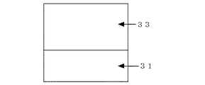
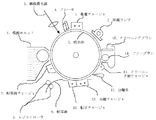
次に、本発明の電子写真感光体の層構成に関して、図1〜5に基づいて説明する。尚、図1〜5は本発明の電子写真感光体を表わす断面図である。
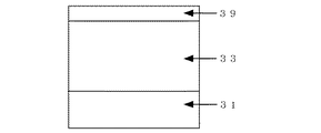
図1の構成においては、導電性支持体31上に、電荷発生物質と電荷輸送物質を主成分とする感光層33が設けられている。
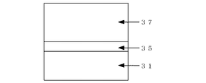
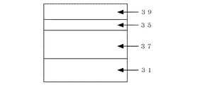
図2の構成においては、導電性支持体31上に、電荷発生物質を主成分とする電荷発生層35と、電荷輸送物質を主成分とする電荷輸送層37とが積層されている。
図3の構成においては、導電性支持体31上に、電荷発生物質と電荷輸送物質を主成分とする感光層33が設けられ、更に感光層表面に保護層39が設けられている。この場合、保護層39に本発明のアミン化合物が含有されても構わない。
図4の構成においては、導電性支持体31上に、電荷発生物質を主成分とする電荷発生層35と電荷輸送物質を主成分とする電荷輸送層37とが積層されており、更に電荷輸送層上に保護層39が設けられている。この場合、保護層39に本発明のアミン化合物が含有されても構わない。
図5の構成においては、導電性支持体31上に、電荷輸送物質を主成分とする電荷輸送層37と電荷発生物質を主成分とする電荷発生層35とが積層されており、更に電荷発生層上に保護層39が設けられている。この場合、保護層39に本発明のアミン化合物が含有されても構わない。
【0026】
本発明の感光体を構成する導電性支持体31としては、体積抵抗1010Ω・cm以下の導電性を示すもの、例えば、アルミニウム、ニッケル、クロム、ニクロム、銅、金、銀、白金などの金属、酸化スズ、酸化インジウムなどの金属酸化物を、蒸着またはスパッタリングにより、フィルム状もしくは円筒状のプラスチック、紙に被覆したもの、あるいは、アルミニウム、アルミニウム合金、ニッケル、ステンレスなどの板およびそれらを、押し出し、引き抜きなどの工法で素管化後、切削、超仕上げ、研摩などの表面処理した管などを使用することができる。また、特開昭52−36016号公報に開示されたエンドレスニッケルベルト、エンドレスステンレスベルトも導電性支持体31として用いることができる。
【0027】
この他、上記支持体上に導電性粉体を適当な結着樹脂に分散して塗工したものについても、本発明の導電性支持体31として用いることができる。この導電性粉体としては、カーボンブラック、アセチレンブラック、またアルミニウム、ニッケル、鉄、ニクロム、銅、亜鉛、銀などの金属粉、あるいは導電性酸化スズ、ITOなどの金属酸化物粉体などがあげられる。また、同時に用いられる結着樹脂には、ポリスチレン、スチレン−アクリロニトリル共重合体、スチレン−ブタジエン共重合体、スチレン−無水マレイン酸共重合体、ポリエステル、ポリ塩化ビニル、塩化ビニル−酢酸ビニル共重合体、ポリ酢酸ビニル、ポリ塩化ビニリデン、ポリアリレート樹脂、フェノキシ樹脂、ポリカーボネート、酢酸セルロース樹脂、エチルセルロース樹脂、ポリビニルブチラール、ポリビニルホルマール、ポリビニルトルエン、ポリ−N−ビニルカルバゾール、アクリル樹脂、シリコーン樹脂、エポキシ樹脂、メラミン樹脂、ウレタン樹脂、フェノール樹脂、アルキッド樹脂などの熱可塑性、熱硬化性樹脂または光硬化性樹脂が挙げられる。このような導電性層は、これらの導電性粉体と結着樹脂を適当な溶剤、例えば、テトラヒドロフラン、ジクロロメタン、メチルエチルケトン、トルエンなどに分散して塗布することにより設けることができる。
【0028】
さらに、適当な円筒基体上にポリ塩化ビニル、ポリプロピレン、ポリエステル、ポリスチレン、ポリ塩化ビニリデン、ポリエチレン、塩化ゴム、テフロン(R)などの素材に前記導電性粉体を含有させた熱収縮チューブによって導電性層を設けてなるものも、本発明の導電性支持体31として良好に用いることができる。
【0029】
次に、本発明の感光体を構成する感光層について説明する。感光層は単層でも積層でもよいが、説明の都合上、先ず電荷発生層35と電荷輸送層37で構成される場合から述べる。尚、感光層を電荷発生層35と電荷輸送層37で構成する場合、下記一般式(1)で表されるジアミン化合物は電荷輸送層37に含有させることが好ましい。
【0030】
感光層を構成する電荷発生層35は、電荷発生物質を主成分とする層である。電荷発生層35には、公知の電荷発生物質を用いることが可能であり、その代表として、シーアイピグメントブルー25(カラーインデックスCI21180)、シーアイピグメントレッド41(CI21200)、シーアイアシッドレッド52(CI45100)、シーアイベーシックレッド3(CI45210)、カルバゾール骨格を有するアゾ顔料(特開昭53−95033号公報に記載)、ジスチリルベンゼン骨格を有するアゾ顔料(特開昭53−133445号公報)、トリフェニルアミン骨格を有するアゾ顔料(特開昭53−132347号公報に記載)、ジベンゾチオフェン骨格を有するアゾ顔料(特開昭54−21728号公報に記載)、オキサジアゾール骨格を有するアゾ顔料(特開昭54−12742号公報に記載)、フルオレノン骨格を有するアゾ顔料(特開昭54−22834号公報に記載)、ビススチルベン骨格を有するアゾ顔料(特開昭54−17733号公報に記載)、ジスチリルオキサジアゾール骨格を有するアゾ顔料(特開昭54−2129号公報に記載)、ジスチリルカルバゾール骨格を有するアゾ顔料(特開昭54−14967号公報に記載)、ベンズアントロン骨格を有するアゾ顔料などのアゾ顔料。例えば、シーアイピグメントブルー16(CI74100)、Y型オキソチタニウムフタロシアニン(特開昭64−17066号公報)、A(β)型オキソチタニウムフタロシアニン、B(α)型オキソチタニウムフタロシアニン、I型オキソチタニウムフタロシアニン(特開平11−21466号公報に記載)、II型クロロガリウムフタロシアニン(飯島他、日本化学会第67春季年回、1B4、04(1994))、V型ヒドロキシガリウムフタロシアニン(大門他、日本化学会第67春季年回、1B4、05(1994))、X型無金属フタロシアニン(米国特許第3,816,118号)などのフタロシアニン系顔料、シーアイバットブラウン5(CI73410)、シーアイバットダイ(CI73030)などのインジコ系顔料、アルゴスカーレットB(バイエル社製)、インタンスレンスカーレットR(バイエル社製)などのペリレン顔料などが挙げられる。なお、これらの材料は単独あるいは2種類以上が併用されても良い。
【0031】
感光層を構成する電荷発生層35は、電荷発生物質を必要に応じて結着樹脂とともに適当な溶剤中にボールミル、アトライター、サンドミル、超音波などを用いて分散し、これを導電性支持体上に塗布し、乾燥することにより形成される。
【0032】
必要に応じて電荷発生層35に用いられる結着樹脂としては、ポリアミド、ポリウレタン、エポキシ樹脂、ポリケトン、ポリカーボネート、シリコーン樹脂、アクリル樹脂、ポリビニルブチラール、ポリビニルホルマール、ポリビニルケトン、ポリスチレン、ポリスルホン、ポリ−N−ビニルカルバゾール、ポリアクリルアミド、ポリビニルベンゾール、ポリエステル、フェノキシ樹脂、塩化ビニル−酢酸ビニル共重合体、ポリ酢酸ビニル、ポリフェニレンオキシド、ポリアミド、ポリビニルピリジン、セルロース系樹脂、カゼイン、ポリビニルアルコール、ポリビニルピロリドン等が挙げられる。結着樹脂の量は、電荷発生物質100重量部に対し0〜500重量部、好ましくは10〜300重量部が適当である。結着樹脂の添加は、分散前あるいは分散後どちらでも構わない。
【0033】
電荷発生層35の形成に用いられる溶剤としては、イソプロパノール、アセトン、メチルエチルケトン、シクロヘキサノン、テトラヒドロフラン、ジオキサン、エチルセルソルブ、酢酸エチル、酢酸メチル、ジクロロメタン、ジクロロエタン、モノクロロベンゼン、シクロヘキサン、トルエン、キシレン、リグロイン等が挙げられるが、特にケトン系溶媒、エステル系溶媒、エーテル系溶媒が良好に使用される。これらは単独で用いても2種以上混合して用いてもよい。
【0034】
電荷発生層35は、電荷発生物質、溶媒及び結着樹脂を主成分とするが、その中には、増感剤、分散剤、界面活性剤、シリコーンオイル等のいかなる添加剤が含まれていても良い。
【0035】
電荷発生層35を形成する際の塗布液の塗工法としては、浸漬塗工法、スプレーコート、ビートコート、ノズルコート、スピナーコート、リングコート等の方法を用いることができる。
電荷発生層35の膜厚は、0.01〜5μm程度が適当であり、好ましくは0.1〜2μmである。
【0036】
感光層を構成する電荷輸送層37は、電荷輸送物質を主成分とする層であり、電荷輸送物質と共に前記一般式(1)で表されるジアミン化合物を含有する。電荷輸送物質については、正孔輸送物質と電子輸送物質、及び高分子電荷輸送物質に分け、以下に説明する。
電荷輸送層37を構成する正孔輸送物質としては、例えば、ポリ−N−カルバゾール及びその誘導体、ポリ−γ−カルバゾリルエチルグルタメート及びその誘導体、ピレン−ホルムアルデヒド縮合物及びその誘導体、ポリビニルピレン、ポリビニルフェナントレン、オキサゾール誘導体、イミダゾール誘導体、トリフェニルアミン誘導体、及び以下の一般式(2)〜(6)、(13)〜(31)で示される化合物が挙げられる。
【0037】
【化24】
【0038】
一般式(13)で表される化合物には、例えば、9−エチルカルバゾール−3−アルデヒド−1−メチル−1−フェニルヒドラゾン、9−エチルカルバゾール−3−アルデヒド−1−ベンジル−1−フェニルヒドラゾン、9−エチルカルバゾール−3−アルデヒド−1,1−ジフェニルヒドラゾンなどがある。
【0039】
【化25】
【0040】
一般式(14)で表される化合物には、例えば、4−ジエチルアミノスチリル−β−アルデヒド−1−メチル−1−フェニルヒドラゾン、4−メトキシナフタレン−1−アルデヒド−1−ベンジル−1−フェニルヒドラゾンなどがある。
【0041】
【化26】
【0042】
一般式(15)で表される化合物には、例えば、4−メトキシベンズアルデヒド−1−メチル−1−フェニルヒドラゾン、2,4−ジメトキシベンズアルデヒド−1−ベンジル−1−フェニルヒドラゾン、4−ジエチルアミノベンズアルデヒド−1,1−ジフェニルヒドラゾン、4−メトキシベンズアルデヒド−1−(4−メトキシ)フェニルヒドラゾン、4−ジフェニルアミノベンズアルデヒド−1−ベンジル−1−フェニルヒドラゾン、4−ジベンジルアミノベンズアルデヒド−1,1−ジフェニルヒドラゾンなどがある。
【0043】
【化27】
【0044】
一般式(16)で表される化合物には、例えば、1,1−ビス(4−ジベンジルアミノフェニル)プロパン、トリス(4−ジエチルアミノフェニル)メタン、2,2’−ジメチル−4,4’−ビス(ジエチルアミノ)−トリフェニルメタンなどがある。
【0045】
【化28】
【0046】
一般式(17)で表される化合物には、例えば、9−(4−ジエチルアミノスチリル)アントラセン、9−ブロム−10−(4−ジエチルアミノスチリル)アントラセンなどがある。
【0047】
【化29】
【0048】
【化30】
【0049】
一般式(18)で表される化合物には、例えば、9−(4−ジメチルアミノベンジリデン)フルオレン、3−(9−フルオレニリデン)−9−エチルカルバゾールなどがある。
【0050】
【化32】
【0051】
一般式(21)で表される化合物には、例えば、1,2−ビス(4−ジエチルアミノスチリル)ベンゼン、1,2−ビス(2,4−ジメトキシスチリル)ベンゼンなどがある。
【0052】
【化33】
【0053】
一般式(22)で表される化合物には、例えば、3−スチリル−9−エチルカルバゾール、3−(4−メトキシスチリル)−9−エチルカルバゾールなどがある。
【0054】
【化34】
【0055】
一般式(23)で表される化合物には、例えば、4−ジフェニルアミノスチルベン、4−ジベンジルアミノスチルベン、4−ジトリルアミノスチルベン、1−(4−ジフェニルアミノスチリル)ナフタレンなどがある。
【0056】
【化35】
【0057】
【化36】
【化37】
【0059】
【化38】
【0060】
一般式(2)で表される化合物には、例えば、4’−ジフェニルアミノ−α−フェニルスチルベン、4’−ビス(4−メチルフェニル)アミノ−α−フェニルスチルベンなどがある。
【0061】
【化39】
【0062】
一般式(24)で表される化合物には、例えば、1−フェニル−3−(4−ジエチルアミノスチリル)−5−(4−ジエチルアミノフェニル)ピラゾリンなどがある。
【0063】
【化40】
【0064】
一般式(25)で表される化合物には、例えば、2,5−ビス(4−ジエチルアミノフェニル)−1,3,4−オキサジアゾール、2−N,N−ジフェニルアミノ−5−(4−ジエチルアミノフェニル)−1,3,4−オキサジアゾール、2−(4−ジメチルアミノフェニル)−5−(4−ジエチルアミノフェニル)−1,3,4−オキサジアゾールなどがある。
【0065】
【化41】
【0066】
一般式(26)で表される化合物には、例えば、2−N,N−ジフェニルアミノ−5−(N−エチルカルバゾール−3−イル)−1,3,4−オキサジアゾール、2−(4−ジエチルアミノフェニル)−5−(N−エチルカルバゾール−3−イル)−1,3,4−オキサジアゾールなどがある。
【0067】
【化42】
【0068】
一般式(27)で表されるベンジジン化合物には、例えば、N,N’−ジフェニル−N,N’−ビス(3−メチルフェニル)−[1,1’−ビフェニル]−4,4’−ジアミン、3,3’−ジメチル−N,N,N’,N’−テトラキス(4−メチルフェニル)−[1,1’−ビフェニル]−4,4’−ジアミンなどがある。
【0069】
【化43】
【0070】
また、一般式(6)で表されるビフェニリルアミン化合物には、例えば、4’−メトキシ−N,N−ジフェニル−[1,1’−ビフェニル]−4−アミン、4’−メチル−N,N−ビス(4−メチルフェニル)−[1,1’−ビフェニル]−4−アミン、4’−メトキシ−N,N−ビス(4−メチルフェニル)−[1,1’−ビフェニル]−4−アミン、N,N−ビス(3,4−ジメチルフェニル)−[1,1’−ビフェニル]−4−アミンなどがある。
【0071】
【化44】
【0072】
一般式(28)で表されるトリアリールアミン化合物には、例えば、N,N−ジフェニル−ピレン−1−アミン、N,N−ジ−p−トリル−ピレン−1−アミン、N,N−ジ−p−トリル−1−ナフチルアミン、N,N−ジ(p−トリル)−1−フェナントリルアミン、9,9−ジメチル−2−(ジ−p−トリルアミノ)フルオレン、N,N,N’,N’−テトラキス(4−メチルフェニル)−フェナントレン−9,10−ジアミン、N,N,N’,N’−テトラキス(3−メチルフェニル)−m−フェニレンジアミンなどがある。
【0073】
【化45】
![]()
【0074】
【化46】
【0075】
一般式(29)で表されるジオレフィン芳香族化合物には、例えば、1,4−ビス(4−ジフェニルアミノスチリル)ベンゼン、1,4−ビス[4−ジ(p−トリル)アミノスチリル]ベンゼンなどがある。
【0076】
【化47】
【0077】
一般式(31)で表されるスチリルピレン化合物には、例えば、1−(4−ジフェニルアミノスチリル)ピレン、1−(N,N−ジ−p−トリル−4−アミノスチリル)ピレンなどがある。
【0078】
本発明においては、以上説明した電荷輸送物質の中でも、一般式(2)(6)で表されるものが好ましい。これらは低分子電荷輸送物質の中でも特に移動度特性、電荷発生材料からの電荷注入特性、並びに繰り返し静電疲労特性が優れるものであるため、感光層中に用いることにより高感度かつ安定な電子写真感光体が得られるものである。
【0079】
また、電荷輸送層37を構成する電子輸送物質としては、例えば、クロルアニル、ブロムアニル、テトラシアノエチレン、テトラシアノキノジメタン、2,4,7−トリニトロ−9−フルオレノン、2,4,5,7−テトラニトロ−9−フルオレノン、2,4,5,7−テトラニトロキサントン、2,4,8−トリニトロチオキサントン、2,6,8−トリニトロ−インデノ4H−インデノ[1,2−b]チオフェン−4−オン、1,3,7−トリニトロジベンゾチオフェン−5,5−ジオキサイドなどを挙げることができ、さらに下記一般式(32)〜(35)で表される電子輸送物質を好適に使用することができる。
これらの電荷輸送物質は単独または2種類以上混合して用いられる。
【0080】
【化48】
【0081】
【化49】
【0082】
【化50】
【0083】
【化51】
【0084】
【化52】
−O−R3 (36)
(36)式中、R3は、置換基を有してもよいアルキル基、または置換基を有してもよいアリール基を示す。〕
【0085】
電荷輸送層37を構成する結着樹脂としては、ポリスチレン、スチレン−アクリロニトリル共重合体、スチレン−ブタジエン共重合体、スチレン−無水マレイン酸共重合体、ポリエステル、ポリ塩化ビニル、塩化ビニル−酢酸ビニル共重合体、ポリ酢酸ビニル、ポリ塩化ビニリデン、ポリアリレート樹脂、フェノキシ樹脂、ポリカーボネート、酢酸セルロース樹脂、エチルセルロース樹脂、ポリビニルブチラール、ポリビニルホルマール、ポリビニルトルエン、ポリ−N−ビニルカルバゾール、アクリル樹脂、シリコーン樹脂、エポキシ樹脂、メラミン樹脂、ウレタン樹脂、フェノール樹脂、アルキッド樹脂等の熱可塑性または熱硬化性樹脂が挙げられる。
【0086】
電荷輸送物質と一般式(1)で表されるジアミン化合物は電荷輸送層内に混合含有される場合、その合計量は、結着樹脂100重量部に対し、20〜300重量部が好ましく、40〜150重量部がより好ましい。また、電荷輸送層の膜厚は解像度・応答性の点から、25μm以下とすることが好ましい。下限値に関しては、使用するシステム(特に帯電電位等)に異なるが、5μm以上が好ましい。
【0087】
また、一般式(1)で表されるアミン化合物の含有量は、電荷輸送物質に対して0.01wt%〜150wt%が好ましい。該アミン化合物が少ないと酸化性ガスに対する耐性が不足し、多すぎると、繰り返し使用による残留電位の上昇が大きくなる。
【0088】
電荷輸送層37を形成する際に用いられる溶剤としては、テトラヒドロフラン、ジオキサン、トルエン、ジクロロメタン、モノクロロベンゼン、ジクロロエタン、シクロヘキサノン、メチルエチルケトン、アセトンなどが用いられる。電荷輸送物質は単独で使用しても2種以上混合して使用しても良い。
【0089】
電荷輸送層37に添加される酸化防止剤としては、後述される一般の酸化防止剤が使用できるが、(c)ハイドロキノン系、及び(f)ヒンダードアミン系の化合物が特に効果的である。但し、ここで用いられる酸化防止剤は、後述の目的と異なり、あくまでも本発明に用いられるジアミン化合物の変質保護のために利用される。このため、これらの酸化防止剤は、ジアミン化合物を含有させる前の工程で塗工液に含有させておくことが好ましく、添加量としては、ジアミン化合物に対して0.1〜200wt%で十分な効果を発揮できる。
【0090】
電荷輸送層37には電荷輸送物質としての機能とバインダー樹脂としての機能を持った高分子電荷輸送物質も良好に使用される。これらの高分子電荷輸送物質から構成される電荷輸送層は耐摩耗性に優れたものである。高分子電荷輸送物質としては、公知の材料が使用できるが、特に、トリアリールアミン構造を主鎖および/または側鎖に含むポリカーボネートが良好に用いられる。中でも、以下の一般式(7)〜(10)、(37)〜(45)で表される化合物が良好に用いられる。
【0091】
【化53】
【0092】
【化54】
【0093】
【化55】
【0094】
【化56】
【0095】
【化57】
【0096】
【化58】
【0097】
【化59】
【0098】
【化60】
【0099】
【化61】
【0100】
【化62】
【0101】
【化63】
【0102】
【化64】
【0103】
【化65】
【0104】
電荷輸送層37は、電荷輸送物質単独もしくは結着樹脂と適当な溶剤に溶解ないし分散し、これを電荷発生層上に塗布、乾燥することにより形成できる。また、必要により単独あるいは2種以上の可塑剤、レベリング剤、酸化防止剤等を添加することもできる。
以上のようにして得られた塗工液の塗工法としては、浸漬塗工法、スプレーコート、ビートコート、ノズルコート、スピナーコート、リングコート等、従来の塗工方法を用いることができる。
【0105】
本発明においては、以上説明した高分子型電荷輸送物質の中でも、一般式(7)(10)で表されるものが好ましい。これらは高分子型電荷輸送物質の中でも耐摩耗性に優れ、かつ高移動度特性を示すものであるので、感光層に用いることにより高耐久かつ高感度な感光体が得られるものである。
【0106】
次に、感光層が単層(図1、図3)の場合について述べる。該感光層33は、電荷発生物質および電荷輸送物質および結着樹脂を適当な溶剤に溶解ないし分散し、これを塗布、乾燥することによって形成できる。また、必要により可塑剤やレベリング剤、酸化防止剤等を添加することもできる。電荷発生物質としては、前述した、複層の場合の電荷発生層35に用いたものと同じものが挙げられる。
【0107】
感光層を単層で構成する場合の結着樹脂としては、先に電荷輸送層37で挙げた結着樹脂のほかに、電荷発生層35で挙げた結着樹脂を混合して用いてもよい。もちろん、先に挙げた高分子電荷輸送物質も良好に使用できる。結着樹脂100重量部に対する電荷発生物質の量は5〜40重量部が好ましく、電荷輸送物質の量は0〜190重量部が好ましく、さらに好ましくは50〜150重量部である。感光層は、電荷発生物質、結着樹脂を電荷輸送物質とともにテトラヒドロフラン、ジオキサン、ジクロロエタン、シクロヘキサン等の溶媒を用いて分散機等で分散した塗工液を、浸漬塗工法やスプレーコート、ビードコート、リングコートなどで塗工して形成できる。感光層の膜厚は、5〜25μm程度が適当である。
【0108】
本発明の感光体においては、導電性支持体31と感光層との間に下引き層を設けることができる。下引き層は一般には樹脂を主成分とするが、これらの樹脂はその上に感光層を溶剤で塗布することを考えると、一般の有機溶剤に対して耐溶剤性の高い樹脂であることが望ましい。このような樹脂としては、ポリビニルアルコール、カゼイン、ポリアクリル酸ナトリウム等の水溶性樹脂、共重合ナイロン、メトキシメチル化ナイロン等のアルコール可溶性樹脂、ポリウレタン、メラミン樹脂、フェノール樹脂、アルキッド−メラミン樹脂、エポキシ樹脂等、三次元網目構造を形成する硬化型樹脂等が挙げられる。また、下引き層にはモアレ防止、残留電位の低減等のために酸化チタン、シリカ、アルミナ、酸化ジルコニウム、酸化スズ、酸化インジウム等で例示できる金属酸化物の微粉末顔料を加えてもよい。
【0109】
これらの下引き層は、前述の感光層の如く適当な溶媒及び塗工法を用いて形成することができる。更に本発明の下引き層として、シランカップリング剤、チタンカップリング剤、クロムカップリング剤等を使用することもできる。この他、本発明の下引き層には、Al2O3を陽極酸化にて設けたものや、ポリパラキシリレン(パリレン)等の有機物やSiO2、SnO2、TiO2、ITO、CeO2等の無機物を真空薄膜作成法にて設けたものも良好に使用できる。このほかにも公知のものを用いることができる。下引き層の膜厚は0〜5μmが適当である。
【0110】
本発明の感光体においては、感光層保護の目的で、保護層39が感光層の上に設けられることがある。保護層39に使用される材料としてはABS樹脂、ACS樹脂、オレフィン−ビニルモノマー共重合体、塩素化ポリエーテル、アリール樹脂、フェノール樹脂、ポリアセタール、ポリアミド、ポリアミドイミド、ポリアクリレート、ポリアリルスルホン、ポリブチレン、ポリブチレンテレフタレート、ポリカーボネート、ポリエーテルスルホン、ポリエチレン、ポリエチレンテレフタレート、ポリイミド、アクリル樹脂、ポリメチルベンテン、ポリプロピレン、ポリフェニレンオキシド、ポリスルホン、ポリスチレン、ポリアリレート、AS樹脂、ブタジエン−スチレン共重合体、ポリウレタン、ポリ塩化ビニル、ポリ塩化ビニリデン、エポキシ樹脂等の樹脂が挙げられる。フィラーの分散性、残留電位、塗膜欠陥の点から、特にポリカーボネートあるいはポリアリレートが有効かつ有用である。
【0111】
また、感光体の保護層には、耐摩耗性を向上する目的でフィラ−材料を添加される。
用いられる溶剤としては、テトラヒドロフラン、ジオキサン、トルエン、ジクロロメタン、モノクロロベンゼン、ジクロロエタン、シクロヘキサノン、メチルエチルケトン、アセトンなど、電荷輸送層37で使用されるすべての溶剤を使用することができる。但し、分散時には粘度が高い溶剤が好ましいが、塗工時には揮発性が高い溶剤が好ましい。これらの条件を満たす溶剤がない場合には、各々の物性を有する溶剤を2種以上混合させて使用することが可能であり、フィラーの分散性や残留電位に対して大きな効果を有する場合がある。
【0112】
また、保護層39に本発明のアミン化合物が含まれていてもよい。さらに電荷輸送層37で挙げた低分子電荷輸送物質あるいは高分子電荷輸送物質を添加することは、残留電位の低減及び画質向上に対して有効かつ有用である。
保護層の形成法としては、浸漬塗工法、スプレーコート、ビートコート、ノズルコート、スピナーコート、リングコート等の従来方法を用いることができるが、特に塗膜の均一性の面からスプレーコートがより好ましい。
【0113】
本発明の感光体においては、感光層と保護層との間に中間層を設けることも可能である。中間層には、一般にバインダー樹脂を主成分として用いる。これら樹脂としては、ポリアミド、アルコール可溶性ナイロン、水溶性ポリビニルブチラール、ポリビニルブチラール、ポリビニルアルコールなどが挙げられる。中間層の形成法としては、前述のごとく一般に用いられる塗布法が採用される。なお、中間層の厚さは0.05〜2μm程度が適当である。
【0114】
本発明においては、耐環境性の改善のため、とりわけ、感度低下、残留電位の上昇を防止する目的で、電荷発生層、電荷輸送層、下引き層、保護層、中間層等の各層に酸化防止剤、可塑剤、滑剤、紫外線吸収剤およびレベリング剤を添加することが出来る。これらの化合物の代表的な材料を以下に記す。
【0115】
本発明の感光体を構成する各層に添加できる酸化防止剤として、例えば下記のものが挙げられる。但し、本発明はこれらに限定されるものではない。
【0116】
(a)フェノール系化合物
2,6−ジ−t−ブチル−p−クレゾール、ブチル化ヒドロキシアニソ−ル、2,6−ジ−t−ブチル−4−エチルフェノール、n−オクタデシル−3−(4’−ヒドロキシ−3’,5’−ジ−t−ブチルフェノール)、2,2’−メチレン−ビス−(4−メチル−6−t−ブチルフェノール)、2,2’−メチレン−ビス−(4−エチル−6−t−ブチルフェノール)、4,4’−チオビス−(3−メチル−6−t−ブチルフェノール)、4,4’−ブチリデンビス−(3−メチル−6−t−ブチルフェノール)、1,1,3−トリス−(2−メチル−4−ヒドロキシ−5−t−ブチルフェニル)ブタン、1,3,5−トリメチル−2,4,6−トリス(3,5−ジ−t−ブチル−4−ヒドロキシベンジル)ベンゼン、テトラキス−[メチレン−3−(3’,5’−ジ−t−ブチル−4’−ヒドロキシフェニル)プロピオネート]メタン、ビス[3,3’−ビス(4’−ヒドロキシ−3’−t−ブチルフェニル)ブチリックアッシド]グリコールエステル、トコフェロ−ル類など。
【0117】
(b)パラフェニレンジアミン類
N−フェニル−N’−イソプロピル−p−フェニレンジアミン、N,N’−ジ−sec−ブチル−p−フェニレンジアミン、N−フェニル−N−sec−ブチル−p−フェニレンジアミン、N,N’−ジ−イソプロピル−p−フェニレンジアミン、N,N’−ジメチル−N,N’−ジ−t−ブチル−p−フェニレンジアミンなど。
【0118】
(c)ハイドロキノン類
2,5−ジ−t−オクチルハイドロキノン、2,6−ジドデシルハイドロキノン、2−ドデシルハイドロキノン、2−ドデシル−5−クロロハイドロキノン、2−t−オクチル−5−メチルハイドロキノン、2−(2−オクタデセニル)−5−メチルハイドロキノンなど。
【0119】
(d)有機硫黄化合物類
ジラウリル−3,3’−チオジプロピオネート、ジステアリル−3,3’−チオジプロピオネート、ジテトラデシル−3,3’−チオジプロピオネートなど。
【0120】
(e)有機燐化合物類
トリフェニルホスフィン、トリ(ノニルフェニル)ホスフィン、トリ(ジノニルフェニル)ホスフィン、トリクレジルホスフィン、トリ(2,4−ジブチルフェノキシ)ホスフィンなど。
【0121】
本発明の感光体を構成する各層に添加できる可塑剤として、例えば下記のものが挙げられる。但し、本発明はこれらに限定されるものではない。
(a)リン酸エステル系可塑剤
リン酸トリフェニル、リン酸トリクレジル、リン酸トリオクチル、リン酸オクチルジフェニル、リン酸トリクロルエチル、リン酸クレジルジフェニル、リン酸トリブチル、リン酸トリ−2−エチルヘキシル、リン酸トリフェニルなど。
【0122】
(b)フタル酸エステル系可塑剤
フタル酸ジメチル、フタル酸ジエチル、フタル酸ジイソブチル、フタル酸ジブチル、フタル酸ジヘプチル、フタル酸ジ−2−エチルヘキシル、フタル酸ジイソオクチル、フタル酸ジ−n−オクチル、フタル酸ジノニル、フタル酸ジイソノニル、フタル酸ジイソデシル、フタル酸ジウンデシル、フタル酸ジトリデシル、フタル酸ジシクロヘキシル、フタル酸ブチルベンジル、フタル酸ブチルラウリル、フタル酸メチルオレイル、フタル酸オクチルデシル、フマル酸ジブチル、フマル酸ジオクチルなど。
【0123】
(c)芳香族カルボン酸エステル系可塑剤
トリメリット酸トリオクチル、トリメリット酸トリ−n−オクチル、オキシ安息香酸オクチルなど。
【0124】
(d)脂肪族二塩基酸エステル系可塑剤
アジピン酸ジブチル、アジピン酸ジ−n−ヘキシル、アジピン酸ジ−2−エチルヘキシル、アジピン酸ジ−n−オクチル、アジピン酸−n−オクチル−n−デシル、アジピン酸ジイソデシル、アジピン酸ジカプリル、アゼライン酸ジ−2−エチルヘキシル、セバシン酸ジメチル、セバシン酸ジエチル、セバシン酸ジブチル、セバシン酸ジ−n−オクチル、セバシン酸ジ−2−エチルヘキシル、セバシン酸ジ−2−エトキシエチル、コハク酸ジオクチル、コハク酸ジイソデシル、テトラヒドロフタル酸ジオクチル、テトラヒドロフタル酸ジ−n−オクチルなど。
【0125】
(e)脂肪酸エステル誘導体
オレイン酸ブチル、グリセリンモノオレイン酸エステル、アセチルリシノール酸メチル、ペンタエリスリトールエステル、ジペンタエリスリトールヘキサエステル、トリアセチン、トリブチリンなど。
【0126】
(f)オキシ酸エステル系可塑剤
アセチルリシノール酸メチル、アセチルリシノール酸ブチル、ブチルフタリルブチルグリコレート、アセチルクエン酸トリブチルなど。
【0127】
(g)エポキシ可塑剤
エポキシ化大豆油、エポキシ化アマニ油、エポキシステアリン酸ブチル、エポキシステアリン酸デシル、エポキシステアリン酸オクチル、エポキシステアリン酸ベンジル、エポキシヘキサヒドロフタル酸ジオクチル、エポキシヘキサヒドロフタル酸ジデシルなど。
【0128】
(h)二価アルコールエステル系可塑剤
ジエチレングリコールジベンゾエート、トリエチレングリコールジ−2−エチルブチラートなど。
【0129】
(i)含塩素可塑剤
塩素化パラフィン、塩素化ジフェニル、塩素化脂肪酸メチル、メトキシ塩素化脂肪酸メチルなど。
【0130】
(j)ポリエステル系可塑剤
ポリプロピレンアジペート、ポリプロピレンセバケート、ポリエステル、アセチル化ポリエステルなど。
【0131】
(k)スルホン酸誘導体
p−トルエンスルホンアミド、o−トルエンスルホンアミド、p−トルエンスルホンエチルアミド、o−トルエンスルホンエチルアミド、トルエンスルホン−N−エチルアミド、p−トルエンスルホン−N−シクロヘキシルアミドなど。
【0132】
(l)クエン酸誘導体
クエン酸トリエチル、アセチルクエン酸トリエチル、クエン酸トリブチル、アセチルクエン酸トリブチル、アセチルクエン酸トリ−2−エチルヘキシル、アセチルクエン酸−n−オクチルデシルなど。
【0133】
(m)その他
ターフェニル、部分水添ターフェニル、ショウノウ、2−ニトロジフェニル、ジノニルナフタリン、アビエチン酸メチルなど。
【0134】
本発明の感光体を構成する各層に添加できる滑剤として、例えば下記のものが挙げられる。但し、本発明はこれらに限定されるものではない。
【0135】
(a)炭化水素系化合物
流動パラフィン、パラフィンワックス、マイクロワックス、低重合ポリエチレンなど。
【0136】
(b)脂肪酸系化合物
ラウリン酸、ミリスチン酸、パルチミン酸、ステアリン酸、アラキジン酸、ベヘン酸など。
【0137】
(c)脂肪酸アミド系化合物
ステアリルアミド、パルミチルアミド、オレインアミド、メチレンビスステアロアミド、エチレンビスステアロアミドなど。
【0138】
(d)エステル系化合物
脂肪酸の低級アルコールエステル、脂肪酸の多価アルコールエステル、脂肪酸ポリグリコールエステルなど。
【0139】
(e)アルコール系化合物
セチルアルコール、ステアリルアルコール、エチレングリコール、ポリエチレングリコール、ポリグリセロールなど。
【0140】
(f)金属石けん
ステアリン酸鉛、ステアリン酸カドミウム、ステアリン酸バリウム、ステアリン酸カルシウム、ステアリン酸亜鉛、ステアリン酸マグネシウムなど。
【0141】
(g)天然ワックス
カルナバロウ、カンデリラロウ、蜜ロウ、鯨ロウ、イボタロウ、モンタンロウなど。
【0142】
(h)その他
シリコーン化合物、フッ素化合物など。
【0143】
本発明の感光体を構成する各層に添加できる紫外線吸収剤として、例えば下記のものが挙げられる。但し、本発明はこれらに限定されるものではない。
【0144】
(a)ベンゾフェノン系
2−ヒドロキシベンゾフェノン、2,4−ジヒドロキシベンゾフェノン、2,2’,4−トリヒドロキシベンゾフェノン、2,2’,4,4’−テトラヒドロキシベンゾフェノン、2,2’−ジヒドロキシ4−メトキシベンゾフェノンなど。
【0145】
(b)サルシレート系
フェニルサルシレート、2,4−ジ−t−ブチルフェニル−3,5−ジ−t−ブチル−4−ヒドロキシベンゾエートなど。
【0146】
(c)ベンゾトリアゾール系
(2’−ヒドロキシフェニル)ベンゾトリアゾール、(2’−ヒドロキシ5’−メチルフェニル)ベンゾトリアゾール、(2’−ヒドロキシ3’−ターシャリブチル5’−メチルフェニル)5−クロロベンゾトリアゾール
【0147】
(d)シアノアクリレート系
エチル−2−シアノ−3,3−ジフェニルアクリレート、メチル2−カルボメトキシ3(パラメトキシ)アクリレートなど。
【0148】
(e)クエンチャー(金属錯塩系)
ニッケル(2,2’チオビス(4−t−オクチル)フェノレート)ノルマルブチルアミン、ニッケルジブチルジチオカルバメート、コバルトジシクロヘキシルジチオホスフェートなど。
【0149】
(f)HALS(ヒンダードアミン)
ビス(2,2,6,6−テトラメチル−4−ピペリジル)セバケート、ビス(1,2,2,6,6−ペンタメチル−4−ピペリジル)セバケート、1−[2−〔3−(3,5−ジ−t−ブチル−4−ヒドロキシフェニル)プロピオニルオキシ〕エチル]−4−〔3−(3,5−ジ−t−ブチル−4−ヒドロキシフェニル)プロピオニルオキシ〕−2,2,6,6−テトラメチルピリジン、8−ベンジル−7,7,9,9−テトラメチル−3−オクチル−1,3,8−トリアザスピロ〔4,5〕ウンデカン−2,4−ジオン、4−ベンゾイルオキシ−2,2,6,6−テトラメチルピペリジンなど。
【0150】
次に図面を用いて本発明の画像形成方法ならびに画像形成装置について詳しく説明する。尚、画像形成方法についてはその代表として電子写真方法について説明し、画像形成装置についてはその代表として電子写真装置について説明する。図6は、本発明の電子写真プロセス及び電子写真装置を説明するための概略図であり、下記のような例も本発明の範疇に属するものである。
図6において、感光体1は少なくとも感光層が設けられ、最表面層にフィラーを含有してなる。感光体1はドラム状の形状を示しているが、シート状、エンドレスベルト状のものであっても良い。帯電チャージャー3、転写前チャージャー7、転写チャージャー10、分離チャージャー11、クリーニング前チャージャー13には、コロトロン、スコロトロン、固体帯電器(ソリッド・ステート・チャージャー)、帯電ローラ等が用いられ、公知の手段がすべて使用可能である。転写手段には、一般に上記の帯電器が使用できるが、図に示されるように転写チャージャーと分離チャージャーを併用したものが効果的である。
【0151】
また、画像露光部5、除電ランプ2等の光源には、蛍光灯、タングステンランプ、ハロゲンランプ、水銀灯、ナトリウム灯、発光ダイオード(LED)、半導体レーザー(LD)、エレクトロルミネッセンス(EL)などの発光物全般を用いることができる。そして、所望の波長域の光のみを照射するために、シャープカットフィルター、バンドパスフィルター、近赤外カットフィルター、ダイクロイックフィルター、干渉フィルター、色温度変換フィルターなどの各種フィルターを用いることもできる。
【0152】
光源等は、図6に示される工程の他に光照射を併用した転写工程、除電工程、クリーニング工程、あるいは前露光などの工程を設けることにより、感光体に光が照射される。
さて、現像ユニット6により感光体1上に現像されたトナーは、転写紙9に転写されるが、全部が転写されるわけではなく、感光体1上に残存するトナーも生ずる。このようなトナーは、ファーブラシ14およびブレード15により、感光体より除去される。クリーニングは、クリーニングブラシだけで行なわれることもあり、クリーニングブラシにはファーブラシ、マグファーブラシを始めとする公知のものが用いられる。
【0153】
電子写真感光体に正(負)帯電を施し、画像露光を行うと、感光体表面上には正(負)の静電潜像が形成される。これを負(正)極性のトナー(検電微粒子)で現像すれば、ポジ画像が得られるし、また正(負)極性のトナーで現像すれば、ネガ画像が得られる。
かかる現像手段には、公知の方法が適用されるし、また、除電手段にも公知の方法が用いられる。
【0154】
図7には、本発明による電子写真プロセスの別の例を示す。感光体21は少なくとも感光層を有し、さらに最表面層にフィラーを含有しており、駆動ローラ22a、22bにより駆動され、帯電器23による帯電、光源24による像露光、現像(図示せず)、帯電器25を用いる転写、光源26によるクリーニング前露光、ブラシ27によるクリーニング、光源28による除電が繰返し行なわれる。第7図においては、感光体21(勿論この場合は支持体が透光性である)に支持体側よりクリーニング前露光の光照射が行なわれる。
【0155】
以上の図示した電子写真プロセスは、本発明における実施形態を例示するものであって、もちろん他の実施形態も可能である。例えば、第7図において支持体側よりクリーニング前露光を行っているが、これは感光層側から行ってもよいし、また、像露光、除電光の照射を支持体側から行ってもよい。
一方、光照射工程は、像露光、クリーニング前露光、除電露光が図示されているが、他に転写前露光、像露光のプレ露光、およびその他公知の光照射工程を設けて、感光体に光照射を行うこともできる。
【0156】
以上に示すような画像形成手段は、複写装置、ファクシミリ、プリンター内に固定して組み込まれていてもよいが、プロセスカートリッジの形でそれら装置内に組み込まれてもよい。プロセスカートリッジとは、感光体を内蔵し、他に帯電手段、露光手段、現像手段、転写手段、クリーニング手段、除電手段を含んだ1つの装置(部品)である。プロセスカートリッジの形状等は多く挙げられるが、一般的な例として、図8に示すものが挙げられる。感光体16は、導電性支持体上に、少なくとも感光層を有し、かつ最表面層にフィラーを含有してなる。
【0157】
【実施例】
以下、本発明について実施例を挙げて説明するが、本発明が実施例により制約を受けるものではない。なお、部はすべて重量部である。
【0158】
実施例1
アルミニウムシリンダー上に下記組成の下引き層塗工液、電荷発生層塗工液、および電荷輸送層塗工液を、浸漬塗工によって順次塗布、乾燥し、3.5μmの下引き層、0.2μmの電荷発生層、23μmの電荷輸送層を形成した(感光体1)。
【0159】
◎下引き層塗工液
二酸化チタン粉末: 400部
メラミン樹脂: 65部
アルキッド樹脂: 120部
2−ブタノン: 400部
【0160】
◎電荷発生層塗工液
下記構造式(46)のフルオレノン系ビスアゾ顔料: 12部
ポリビニルブチラール: 5部
2−ブタノン: 200部
シクロヘキサノン: 400部
【化66】
◎電荷輸送層塗工液
ポリカーボネート樹脂(Zポリカ、帝人化成製): 10部
例示化合物No.1のジアミン化合物: 10部
テトラヒドロフラン: 100部
【0162】
以上のように作製した電子写真感光体を、電子写真プロセス用カートリッジに装着し、帯電方式をコロナ帯電方式(スコロトロン型)、画像露光光源を655nmの半導体レーザー(LD)を用いたリコー製imagioMF2200改造機にて暗部電位800(−V)に設定した後、連続してトータル10万枚印刷相当の繰り返し試験をおこなった。その際、初期画像及び繰り返し試験後の画像について評価を行った。また、初期及び繰り返し試験後の明部電位も測定した。結果を表4に示す。
【0163】
実施例2〜15
実施例1において、例示化合物No.1のジアミン化合物の代わりに表4に示す例示化合物No.のジアミン化合物を用いた以外は、すべて実施例1と同様にして、電子写真感光体2〜15を作製し、評価した。結果を表4に示す。
【0164】
【表4】
実施例16
実施例1における電荷輸送層塗工液を、下記組成のものに変更した以外は、すべて実施例1と同様にして、電子写真感光体7を作製した。
【0166】
◎電荷輸送層塗工液
ポリカーボネート樹脂(Zポリカ、帝人化成製): 10部
例示化合物No.1のジアミン化合物: 1部
下記構造式(47)の電荷輸送物質: 9部
テトラヒドロフラン: 100部
【化67】
実施例17〜30
実施例16において、例示化合物No.1のジアミン化合物の代わりに表5に示す例示化合物No.のジアミン化合物を用いた以外は、すべて実施例16と同様にして、電子写真感光体17〜30を作製し、評価した。結果を同様に表5に示す。
【0168】
【表5】
実施例31〜34
含有されるジアミン化合物と電荷輸送物質の量を下記の量に変更した以外は、実施例16と同様にして、電子写真感光体31〜34を作製し、評価した。結果を同様に表6に示す。
ジアミン化合物: 1部
電荷輸送物質: 7部
【0170】
【表6】
実施例35〜38
実施例16において、含有されるジアミン化合物と電荷輸送物質の量を下記の量に変更した以外は、実施例16と同様にして、電子写真感光体35〜38を作製し、評価した。結果を同様に表8に示す。
ジアミン化合物: 5部
電荷輸送物質: 5部
【0172】
【表7】
実施例39〜42
実施例16において、例示化合物No.1のジアミン化合物を表8に示す例示化合物No.のジアミン化合物に変更し、構造式(47)の電荷輸送物質の代わりに下記構造式(48)の電荷輸送物質を用いた以外は、すべて実施例16と同様にして、電子写真感光体39〜42を作製し、評価した。結果を同様に表8に示す。
【化68】
【表8】
実施例43〜46
実施例16において、例示化合物No.1のジアミン化合物を表9に示す例示化合物No.のジアミン化合物に変更し、構造式(47)の電荷輸送物質の代わりに下記構造式(49)の電荷輸送物質を用いた以外は、すべて実施例16と同様にして、電子写真感光体43〜46を作製し、評価した。結果を同様に表9に示す。
【0176】
【化69】
【表9】
実施例47〜49
実施例16において、例示化合物No.1のジアミン化合物を表10に示す例示化合物No.のジアミン化合物に変更し、電荷輸送層に含有される電荷輸送物質及びバインダー樹脂を下記構造式(50)の材料に変更した以外は、すべて実施例16と同様にして、電子写真感光体47〜49を作製し、評価した。結果を同様に表10に示す。
下記構造式(50)の高分子電荷輸送物質: 19部
【化70】
【表10】
実施例50、51
実施例16において、例示化合物No.1のジアミン化合物を表11に示す例示化合物No.のジアミン化合物に変更し、電荷輸送層に含有される電荷輸送物質及びバインダー樹脂を下記構造式(51)の材料に変更した以外は、すべて実施例16と同様にして、電子写真感光体50、51を作製し、評価した。結果を同様に表11に示す。
下記構造式(51)の高分子電荷輸送物質: 19部
【化71】
【表11】
実施例52、53
実施例16において、例示化合物No.1のジアミン化合物を表12に示す例示化合物No.のジアミン化合物に変更し、電荷輸送層に含有される電荷輸送物質及びバインダー樹脂を下記構造式(52)の材料に変更した以外は、すべて実施例16と同様にして、電子写真感光体52、53を作製し、評価した。結果を同様に表12に示す。
下記構造式(52)の高分子電荷輸送物質: 19部
【化72】
【表12】
実施例54〜57
実施例16において、例示化合物No.1のジアミン化合物を表13に示す例示化合物No.のジアミン化合物に変更し、バインダー樹脂を下記の材料に変更した以外は、すべて実施例16と同様にして、電子写真感光体54〜57を作製し、評価した。結果を同様に表13に示す。
ポリアリレート樹脂(Uポリマー、ユニチカ製): 10部
【0185】
【表13】
実施例58、59
実施例1における電荷発生層塗工液、電荷輸送層塗工液を下記のものに変更した以外は、同様に操作して、電子写真感光体58、59を作製し、評価した。結果を同様に表14に示す。
◎電荷輸送層塗工液
ポリカーボネート樹脂(Zポリカ): 10部
ジアミン化合物: 1部
下記構造式(47)の電荷輸送物質: 7部
トルエン: 70部
【化73】
【表14】
実施例60、61
実施例58における電荷輸送物質を下記構造式(53)の化合物に変更した以外は、同様に操作して、電子写真感光体60、61を作製し、評価した。結果を同様に表15に示す。
【化74】
【表15】
比較例1
実施例16において、ジアミン化合物を下記構造式(54)のスチルベン化合物(特開昭60−196768号公報記載)にした以外は、すべて実施例16と同様にして、比較電子写真感光体1を作製し、評価した。結果を表16に示す。
【化75】
比較例2
実施例16において、電荷輸送層形成用塗工液にジアミン化合物を加えず、電荷輸送物質の重量を10部とした以外は、すべて実施例7と同様にして、比較電子写真感光体2を作製し、評価した。結果を表16に示す。
【0193】
比較例3
実施例35において、ジアミン化合物を下記構造式(55)のテトラフェニルメタン化合物(特開2000−231204号公報記載)にした以外は、すべて実施例35と同様にして、比較電子写真感光体3を作製し、評価した。結果を表16に示す。
【化76】
比較例4
実施例16において、ジアミン化合物を下記構造式(56)のヒンダードアミン系酸化防止剤にした以外は、すべて実施例16と同様にして、比較電子写真感光体4を作製し、評価した。結果を表16に示す。
【化77】
【表16】
以上の評価結果から、10万枚印刷後においても明部電位上昇は少なく、本発明のジアミン化合物を含有した感光体では高画質画像が安定に得られることが確認された。一方、比較感光体1、3、4は、明部電位が初期から非常に高く、画像濃度の低下や解像度の低下を引き起こしており、10万枚印刷後では階調性が著しく低下したことによって画像の判別が不可能であった。また、比較感光体2は明部電位の上昇は比較的小さいものの、本発明の感光体と比べ、繰り返し使用による解像度低下が大きかった。
【0197】
実施例62〜72、比較例5
また、本発明の電子写真感光体、及び比較感光体2について50ppmの窒素酸化物(NOx)ガス濃度に調整されたデシケータ中に4日間放置し、前後における画像評価を行った。結果を表17に示す。
【0198】
【表17】
表17の評価結果より、感光体に本発明のアミン化合物を含有させることによって、酸化性ガスに対する耐性、すなわち解像度低下抑止が大幅に向上することがわかる。一方、比較感光体2においては初期画像品質は良好であるが、酸化性ガスにより著しい解像度の低下がおこることがわかる。
【0200】
【発明の効果】
本発明によれば、一般式(1)で表されるジアミン化合物を含有することにより、感度低下を招くことなく、繰り返し使用、および酸化性ガスなどに対する環境耐性が大幅に向上するため、高耐久性を有し、長期にわたって高解像度の画質が得られる電子写真感光体を得ることが可能となった。本発明によって、電子写真感光体の高耐久化と高画質化の両立が実現され、高画質画像が長期に渡って安定に得られる電子写真感光体、及びそれを用いた画像形成方法、画像形成装置、画像形成装置用プロセスカートリッジが提供される。
【図面の簡単な説明】
【図1】本発明の電子写真感光体の一例を表わす断面図である。
【図2】本発明の電子写真感光体の他の一例を表わす断面図である。
【図3】本発明の電子写真感光体の他の一例を表わす断面図である。
【図4】本発明の電子写真感光体の他の一例を表わす断面図である。
【図5】本発明の電子写真感光体の他の一例を表わす断面図である。
【図6】本発明の電子写真プロセス及び電子写真装置の一例を示す概略図である。
【図7】本発明の電子写真プロセス及び電子写真装置の他の一例を示す概略図である。
【図8】本発明のプロセスカートリッジの一例を示す概略図である。
【図9】オキソチタニウムフタロシアニンの粉末XDスペクトルである。
【符号の説明】
31 導電性支持体
33 感光層
35 電荷発生層
37 電荷輸送層
39 保護層[0001]
TECHNICAL FIELD OF THE INVENTION
The present invention relates to an electrophotographic photosensitive member, an image forming method using the electrophotographic photosensitive member, an image forming apparatus, and a process cartridge for an image forming apparatus.
[0002]
[Prior art]
2. Description of the Related Art In recent years, there has been a remarkable development of information processing system machines using an electrophotographic system. Particularly, laser printers and digital copiers that convert information into digital signals and record information by light have remarkably improved in print quality and reliability. Further, they have been applied to laser printers or digital copying machines capable of full-color printing by fusing with high-speed technology. From such a background, it is particularly important to achieve both high image quality and high durability as functions required for the photoconductor.
[0003]
As photoreceptors used in these electrophotographic laser printers and digital copiers, those using an organic photosensitive material (OPC) are generally widely used due to reasons such as cost, productivity, and non-pollution. Applied. The layer structure of the OPC photoreceptor is roughly classified into a single layer type and a function-separated type laminated structure. For example, the PVK-TNF charge transfer complex type photoreceptor which is the first practical OPC was the former single-layer type. On the other hand, in 1968, Hayashi and Regensburger independently invented a PVK / a-Se laminated photoreceptor, and later referred to as an organic pigment dispersion layer and an organic low-molecular dispersion polymer layer by Melz et al. In 1977 and Schlosser in 1978. A laminated photoreceptor in which all photosensitive layers are made of an organic material has been announced. These are based on the concept of a charge generation layer (CGL) that absorbs light to generate charges and a charge transport layer (CTL) that injects and transports charges generated by CGL and neutralizes surface charges. It is also called a mold laminated photoreceptor. With the development of this function-separated type photoconductor, the sensitivity and durability have been dramatically improved as compared with the single-layer photoconductor. In addition, since materials having different functions, which are called a charge generation material (CGM) and a charge transport material (CTM), can be individually designed, the selection range of these materials has been greatly increased. For these reasons, the function-separated-type laminated photoconductor has become the mainstream layer configuration in the current OPC photoconductor.
[0004]
The mechanism of electrostatic latent image formation in a function-separated type photoreceptor is that, when the photoreceptor is charged and irradiated with light, the light passes through the charge transport layer and is absorbed by the charge generating substance in the charge generation layer to generate charges. . The generated charge is injected into the charge transport layer at the interface between the charge generation layer and the charge transport layer, and further moves in the charge transport layer by an electric field to neutralize the surface charge of the photoreceptor, thereby forming an electrostatic latent image. It is to form.
[0005]
However, organic photoreceptors suffer significant film scraping due to repeated use, and as the photoreceptor layer scrapes, the charge potential of the photoreceptor decreases, the photosensitivity deteriorates, background contamination due to scratches on the photoreceptor surface, image There is a strong tendency to promote density reduction or image quality degradation. Therefore, the abrasion resistance of the organic photoreceptor has been conventionally cited as a major problem. Furthermore, in recent years, the high durability of the photoconductor has become an even more important issue due to the reduction in the diameter of the photoconductor along with the increase in the speed of the electrophotographic apparatus or the miniaturization of the apparatus.
[0006]
As a method for improving the abrasion resistance of the photoreceptor, a method of imparting lubricating properties to the photosensitive layer, curing the photosensitive layer, or including a filler, or instead of a low molecular charge transport material (CTM) molecular dispersed polymer layer is used. A method using a polymer type charge transport material is widely known. However, if the removal of the photosensitive layer is suppressed by these methods, a new problem occurs. That is, ozone, NOx, and other oxidizing substances generated by repeated use and the surrounding environment are adsorbed on the surface of the photosensitive layer, and depending on the repeated use and the use environment, the outermost surface is reduced in resistance, and image deletion (image blurring) occurs. It is known to cause such problems. Conventionally, the problem has been avoided to some extent by removing the blur-generating material together with the photosensitive layer. However, as described above, a new method has to be added in order to respond to recent demands for higher resolution and higher durability. One method of reducing the influence is to mount a heater on the photoreceptor and evaporate the blurred substance. However, this method is a major obstacle to downsizing the apparatus and reducing power consumption. An additive such as an antioxidant is also an effective means. However, since a simple additive does not have photoconductivity, the addition of a large amount to the photosensitive layer may reduce the sensitivity and increase the residual potential. This leads to problems with photographic properties.
[0007]
As described above, the electrophotographic photoreceptor that imparts high abrasion resistance or has reduced abrasion due to the process design around the photoreceptor can avoid adverse effects on image quality, such as image blurring and reduced resolution as side effects. Therefore, it has been difficult to achieve both high durability and high image quality. This is because a higher resistance is more suitable for suppressing the occurrence of image blur, and a lower resistance is more suitable for suppressing the rise in residual potential. Is difficult to solve.
[0008]
On the other hand, Japanese Patent Application Laid-Open No. 2000-231204 (Patent Document 1) discloses an aromatic compound having a dialkylamino group as an acid scavenger for a photoreceptor. Although this compound is effective for the image quality after repeated use of the photoreceptor and is said to be able to solve the problem of image blurring (image blurring) due to blurring substances such as the oxidizing gas, the charge transport It is difficult to respond to demands for high sensitivity and high speed due to low performance, and therefore there is a limit in the amount of addition.
[0009]
Further, stilbene compounds having a dialkylamino group disclosed in JP-A-60-196768 (Patent Document 2), Japanese Patent No. 2884353 (Patent Document 3) and the like are also resistant to image blur caused by oxidation-resistant gas. The effect is described in [Itami et al., Konica Technical Report, Vol. 13, p. 37, 2000]. However, since the stilbene compound has a dialkylamino group which is a substituent having a strong mesomeric effect (+ M effect) at a resonance site of a triarylamine structure as a charge transport site, the overall ionization potential value is abnormally small. Become. Therefore, the charge retention ability of the photosensitive layer used alone as the charge transport material is significantly deteriorated from the beginning or by repeated use, and has a fatal drawback that practical use is extremely difficult. Also, even when mixed with other charge transporting substances as in the present invention, the stilbene compound has a considerably lower ionization potential value than those, so that the stilbene compound becomes a hole trap site for mobile charges, and the sensitivity is extremely low, and There is a disadvantage that the electrophotographic photosensitive member has a large residual potential.
[0010]
[Patent Document 1]
JP 2000-231204 A
[Patent Document 2]
JP-A-60-196768
[Patent Document 3]
Japanese Patent No. 2884353
[0011]
[Problems to be solved by the invention]
SUMMARY OF THE INVENTION It is an object of the present invention to provide an electrophotographic photosensitive member having high durability even when used repeatedly for a long period of time, and suppressing image deterioration due to image density reduction or image blurring, and stably obtaining a high-quality image. Is to provide the body. In addition, by using these photoconductors, it is not necessary to replace the photoconductors, and it is possible to realize high-speed printing or downsizing of the apparatus due to the reduction in the diameter of the photoconductors. An object of the present invention is to provide an image forming method, an image forming apparatus, and an image forming process cartridge.
[0012]
[Means for Solving the Problems]
As a result of intensive studies, the present inventors have found that by including a specific diamine compound in the photosensitive layer, it is possible to solve the above-mentioned problems such as image blur (image deletion) due to a blur generating substance such as an oxidizing gas. Reached the present invention.
According to the present invention, there are provided an electrophotographic photosensitive member, an image forming method using the electrophotographic photosensitive member, an image forming apparatus, and an image forming process cartridge.
[1] An electrophotographic photosensitive member having a photosensitive layer provided on a conductive support, wherein the photosensitive layer contains a diamine compound represented by the following general formula (1). .
Embedded image
[2] The electrophotographic photosensitive member according to [1], wherein the photosensitive layer contains a charge transport material.
[3] The electrophotographic photosensitive member according to [2], wherein the charge transport material is a stilbene compound represented by the following general formula (2).
Embedded image
Embedded image
Embedded image
[4] The electrophotographic photoreceptor according to [2], wherein the charge transport material is an aminobiphenyl compound represented by the following general formula (6).
Embedded image
[5] The electrophotographic photoreceptor according to the above [2], wherein the charge transport material is a polymer type charge transport material.
[6] The electrophotographic photoreceptor according to the above [5], wherein the polymer type charge transport material is a compound represented by the following general formula (7).
Embedded image
Embedded image
Embedded image
[7] The electrophotographic photoreceptor according to the above [5], wherein the polymer type charge transport material is a compound represented by the following general formula (10).
Embedded image
[8] An image forming method, wherein at least charging, image exposure, development, and transfer are repeatedly performed on the electrophotographic photosensitive member according to any one of [1] to [7].
[9] The electrophotographic photoreceptor according to any one of [1] to [7], wherein at least charging, image exposure, development, and transfer are repeated, and at the time of image exposure, the photoreceptor is driven by an LD or an LED. A digital image forming method, wherein an electrostatic latent image is written thereon.
[10] An image forming apparatus comprising at least a charging unit, an image exposing unit, a developing unit, a transferring unit, and the electrophotographic photosensitive member according to any one of [1] to [7].
[11] At least a charging unit, an image exposing unit, a developing unit, a transferring unit and the electrophotographic photoreceptor according to any one of the above [1] to [7], and an LD or an LED or the like is used as the image exposing unit. A digital image forming apparatus wherein an electrostatic latent image is written on the electrophotographic photosensitive member.
[12] A process cartridge for an image forming apparatus, comprising at least the electrophotographic photosensitive member according to any one of [1] to [7].
[0013]
BEST MODE FOR CARRYING OUT THE INVENTION
Hereinafter, the electrophotographic photosensitive member of the present invention, an image forming method using the electrophotographic photosensitive member, an image forming apparatus, and a process cartridge for the image forming apparatus will be described in detail.
In the electrophotographic photoreceptor of the present invention, a photosensitive layer is provided on a conductive support, and the photosensitive layer contains a diamine compound represented by the following general formula (1); Is a characteristic constituent element of the present invention. First, the diamine compound represented by the general formula (1) will be described in detail.
[0014]
Embedded image
[0015]
The diamine compound represented by the general formula (1) is described as a dye intermediate or a precursor of a polymer compound in Japanese Patent Publication No. 62-13382, U.S. Pat. Nos. 4,223,144, 3,271,383 and 3,291,788. The compound is effective for maintaining image quality when the photoreceptor is used repeatedly. Although the reason is not clear at present, the alkylamino group contained in the chemical structure is a strong basic group. The sum effect is estimated. Also, an aromatic hydrocarbon ring-substituted amino group is known to be a sensitive group having an excellent charge transport ability [Takahashi et al., Journal of the Electrographic Society of Japan, Vol. 25, No. 3, p. 16, 1986], Since the diamine compound used in the present invention contains this group, it is understood that the compound has a high charge transporting ability. Further, it has been found that the use of such a compound together with another charge transporting substance further increases the sensitivity and the repetition stability.
[0016]
The diamine compound represented by the general formula (1) can be easily produced by the method described in the literature (E. Elceand AS Hay, Polymer, Vol. 37 No. 9, 1745 (1996)). That is, a dihalide represented by the following general formula (11) is reacted with a secondary amine compound represented by the following general formula (12) at a temperature from room temperature to about 100 ° C. in the presence of a basic compound. Can be obtained.
[0017]
Embedded image
![]()
[0018]
Embedded image
[0019]
Specific examples of the basic compound include potassium carbonate, sodium carbonate, potassium hydroxide, sodium hydroxide, sodium hydride, sodium methylate, and potassium-t-butoxide. Examples of the reaction solvent include dioxane, tetrahydrofuran, toluene, xylene, dimethyl sulfoxide, N, N-dimethylformamide, N-methylpyrrolidone, 1,3-dimethyl-2-imidazolidinone, and acetonitrile.
[0020]
Specific examples of the alkyl group in the description of the general formulas (1) and (12) include a methyl group, an ethyl group, a propyl group, a butyl group, a hexyl group, and an undecanyl group. Examples of the aromatic hydrocarbon group include an aromatic ring such as benzene, biphenyl, naphthalene, anthracene, fluorene and pyrene, and an aromatic heterocyclic group such as pyridine, quinoline, thiophene, furan, oxazole, oxadiazole and carbazole. No. Examples of these substituents include those exemplified in the above specific examples of the alkyl group, methoxy group, ethoxy group, propoxy group, alkoxy group such as butoxy group, or halogen atom such as fluorine atom, chlorine atom, bromine atom and iodine atom. Atoms, the aromatic hydrocarbon groups, and heterocyclic groups such as pyrrolidine, piperidine, and piperazine. Further, R1, R2Are bonded to each other to form a heterocyclic group containing a nitrogen atom, examples of the heterocyclic group include a condensed heterocyclic group in which an aromatic hydrocarbon group is condensed with a pyrrolidino group, a piperidino group, a piperazino group, or the like.
[0021]
Hereinafter, preferred examples of the compound represented by the general formula (1) will be described. However, the present invention is not limited to these compounds.
[0022]
[Table 1]
[Table 2]
[Table 3]
Next, the layer constitution of the electrophotographic photosensitive member of the present invention will be described with reference to FIGS. 1 to 5 are sectional views showing the electrophotographic photosensitive member of the present invention.
In the configuration shown in FIG. 1, a
In the configuration shown in FIG. 2, a
In the configuration of FIG. 3, a
In the configuration shown in FIG. 4, a
In the configuration shown in FIG. 5, a
[0026]
The conductive support 31 constituting the photoreceptor of the present invention has a volume resistance of 1010What shows conductivity of Ωcm or less, for example, aluminum, nickel, chromium, nichrome, copper, gold, silver, metals such as platinum, tin oxide, metal oxides such as indium oxide, by evaporation or sputtering, by film Or cylindrical plastic or paper-coated, or aluminum, aluminum alloy, nickel, stainless steel, etc. plates and extruded, drawn, etc., made into a tube, then cut, super finished, polished etc. Surface-treated tubes and the like can be used. Further, an endless nickel belt and an endless stainless belt disclosed in JP-A-52-36016 can also be used as the conductive support 31.
[0027]
In addition, a material obtained by dispersing a conductive powder in an appropriate binder resin on the above support and applying the same can also be used as the conductive support 31 of the present invention. Examples of the conductive powder include carbon black, acetylene black, metal powder such as aluminum, nickel, iron, nichrome, copper, zinc and silver, and metal oxide powder such as conductive tin oxide and ITO. Can be The binder resins used simultaneously include polystyrene, styrene-acrylonitrile copolymer, styrene-butadiene copolymer, styrene-maleic anhydride copolymer, polyester, polyvinyl chloride, and vinyl chloride-vinyl acetate copolymer. , Polyvinyl acetate, polyvinylidene chloride, polyarylate resin, phenoxy resin, polycarbonate, cellulose acetate resin, ethyl cellulose resin, polyvinyl butyral, polyvinyl formal, polyvinyl toluene, poly-N-vinyl carbazole, acrylic resin, silicone resin, epoxy resin, Thermoplastic, thermosetting resin or photocurable resin such as melamine resin, urethane resin, phenol resin, and alkyd resin. Such a conductive layer can be provided by dispersing the conductive powder and the binder resin in an appropriate solvent, for example, tetrahydrofuran, dichloromethane, methyl ethyl ketone, toluene, or the like, and applying the dispersion.
[0028]
Further, a conductive material is formed by heat-shrinking a tube made of a material such as polyvinyl chloride, polypropylene, polyester, polystyrene, polyvinylidene chloride, polyethylene, chlorinated rubber, and Teflon (R) on a suitable cylindrical substrate. Those provided with a layer can also be favorably used as the conductive support 31 of the present invention.
[0029]
Next, the photosensitive layer constituting the photoreceptor of the present invention will be described. The photosensitive layer may be a single layer or a stacked layer, but for convenience of explanation, the case where the photosensitive layer is composed of the
[0030]
The
[0031]
The
[0032]
If necessary, the binder resin used for the
[0033]
Examples of the solvent used for forming the
[0034]
The
[0035]
As a method of applying the coating solution when forming the
The thickness of the
[0036]
The
Examples of the hole transport material constituting the
[0037]
Embedded image
[0038]
Examples of the compound represented by the general formula (13) include 9-ethylcarbazole-3-aldehyde-1-methyl-1-phenylhydrazone and 9-ethylcarbazole-3-aldehyde-1-benzyl-1-phenylhydrazone. And 9-ethylcarbazole-3-aldehyde-1,1-diphenylhydrazone.
[0039]
Embedded image
[0040]
Examples of the compound represented by the general formula (14) include 4-diethylaminostyryl-β-aldehyde-1-methyl-1-phenylhydrazone, 4-methoxynaphthalene-1-aldehyde-1-benzyl-1-phenylhydrazone. and so on.
[0041]
Embedded image
[0042]
Examples of the compound represented by the general formula (15) include 4-methoxybenzaldehyde-1-methyl-1-phenylhydrazone, 2,4-dimethoxybenzaldehyde-1-benzyl-1-phenylhydrazone, and 4-diethylaminobenzaldehyde. 1,1-diphenylhydrazone, 4-methoxybenzaldehyde-1- (4-methoxy) phenylhydrazone, 4-diphenylaminobenzaldehyde-1-benzyl-1-phenylhydrazone, 4-dibenzylaminobenzaldehyde-1,1-diphenylhydrazone and so on.
[0043]
Embedded image
[0044]
Examples of the compound represented by the general formula (16) include 1,1-bis (4-dibenzylaminophenyl) propane, tris (4-diethylaminophenyl) methane, and 2,2′-dimethyl-4,4 ′ -Bis (diethylamino) -triphenylmethane.
[0045]
Embedded image
[0046]
Examples of the compound represented by the general formula (17) include 9- (4-diethylaminostyryl) anthracene and 9-bromo-10- (4-diethylaminostyryl) anthracene.
[0047]
Embedded image
[0048]
Embedded image
[0049]
Examples of the compound represented by the general formula (18) include 9- (4-dimethylaminobenzylidene) fluorene and 3- (9-fluorenylidene) -9-ethylcarbazole.
[0050]
Embedded image
[0051]
Examples of the compound represented by the general formula (21) include 1,2-bis (4-diethylaminostyryl) benzene and 1,2-bis (2,4-dimethoxystyryl) benzene.
[0052]
Embedded image
[0053]
Examples of the compound represented by the general formula (22) include 3-styryl-9-ethylcarbazole and 3- (4-methoxystyryl) -9-ethylcarbazole.
[0054]
Embedded image
[0055]
Examples of the compound represented by the general formula (23) include 4-diphenylaminostilbene, 4-dibenzylaminostilbene, 4-ditolylaminostilbene, and 1- (4-diphenylaminostyryl) naphthalene.
[0056]
Embedded image
[0057]
Embedded image
Embedded image
[0059]
Embedded image
[0060]
Examples of the compound represented by the general formula (2) include 4'-diphenylamino-α-phenylstilbene and 4'-bis (4-methylphenyl) amino-α-phenylstilbene.
[0061]
Embedded image
[0062]
Examples of the compound represented by the general formula (24) include 1-phenyl-3- (4-diethylaminostyryl) -5- (4-diethylaminophenyl) pyrazolin.
[0063]
Embedded image
[0064]
Compounds represented by the general formula (25) include, for example, 2,5-bis (4-diethylaminophenyl) -1,3,4-oxadiazole, 2-N, N-diphenylamino-5- (4 -Diethylaminophenyl) -1,3,4-oxadiazole, 2- (4-dimethylaminophenyl) -5- (4-diethylaminophenyl) -1,3,4-oxadiazole and the like.
[0065]
Embedded image
[0066]
Examples of the compound represented by the general formula (26) include 2-N, N-diphenylamino-5- (N-ethylcarbazol-3-yl) -1,3,4-oxadiazole and 2- ( 4-diethylaminophenyl) -5- (N-ethylcarbazol-3-yl) -1,3,4-oxadiazole.
[0067]
Embedded image
[0068]
The benzidine compound represented by the general formula (27) includes, for example, N, N′-diphenyl-N, N′-bis (3-methylphenyl)-[1,1′-biphenyl] -4,4′- Diamine and 3,3′-dimethyl-N, N, N ′, N′-tetrakis (4-methylphenyl)-[1,1′-biphenyl] -4,4′-diamine.
[0069]
Embedded image
[0070]
The biphenylylamine compound represented by the general formula (6) includes, for example, 4′-methoxy-N, N-diphenyl- [1,1′-biphenyl] -4-amine and 4′-methyl-N , N-Bis (4-methylphenyl)-[1,1'-biphenyl] -4-amine, 4'-methoxy-N, N-bis (4-methylphenyl)-[1,1'-biphenyl]- 4-amine, N, N-bis (3,4-dimethylphenyl)-[1,1′-biphenyl] -4-amine and the like.
[0071]
Embedded image
[0072]
Examples of the triarylamine compound represented by the general formula (28) include N, N-diphenyl-pyrene-1-amine, N, N-di-p-tolyl-pyrene-1-amine, N, N- Di-p-tolyl-1-naphthylamine, N, N-di (p-tolyl) -1-phenanthrylamine, 9,9-dimethyl-2- (di-p-tolylamino) fluorene, N, N, N ', N'-Tetrakis (4-methylphenyl) -phenanthrene-9,10-diamine, N, N, N', N'-tetrakis (3-methylphenyl) -m-phenylenediamine and the like.
[0073]
Embedded image
![]()
[0074]
Embedded image
[0075]
Examples of the diolefin aromatic compound represented by the general formula (29) include 1,4-bis (4-diphenylaminostyryl) benzene and 1,4-bis [4-di (p-tolyl) aminostyryl] There is benzene.
[0076]
Embedded image
[0077]
Examples of the styrylpyrene compound represented by the general formula (31) include 1- (4-diphenylaminostyryl) pyrene and 1- (N, N-di-p-tolyl-4-aminostyryl) pyrene.
[0078]
In the present invention, among the charge transport materials described above, those represented by the general formulas (2) and (6) are preferable. Among these low-molecular-weight charge transport materials, they have excellent mobility characteristics, charge injection characteristics from charge-generating materials, and repetitive electrostatic fatigue characteristics. A photoreceptor is obtained.
[0079]
Examples of the electron transporting material constituting the
These charge transport materials are used alone or in combination of two or more.
[0080]
Embedded image
[0081]
Embedded image
[0082]
Embedded image
[0083]
Embedded image
[0084]
Embedded image
-OR3 (36)
(36) where R3Represents an alkyl group which may have a substituent or an aryl group which may have a substituent. ]
[0085]
Examples of the binder resin constituting the
[0086]
When the charge transport material and the diamine compound represented by the general formula (1) are mixed and contained in the charge transport layer, the total amount is preferably 20 to 300 parts by weight, and more preferably 40 to 40 parts by weight, based on 100 parts by weight of the binder resin. ~ 150 parts by weight is more preferred. Further, the thickness of the charge transport layer is preferably 25 μm or less from the viewpoint of resolution and response. The lower limit varies depending on the system used (especially the charged potential and the like), but is preferably 5 μm or more.
[0087]
Further, the content of the amine compound represented by the general formula (1) is preferably 0.01 wt% to 150 wt% with respect to the charge transporting substance. When the amount of the amine compound is small, the resistance to the oxidizing gas is insufficient, and when the amount is too large, the residual potential increases due to repeated use.
[0088]
As a solvent used for forming the
[0089]
As the antioxidant added to the
[0090]
For the
[0091]
Embedded image
[0092]
Embedded image
[0093]
Embedded image
[0094]
Embedded image
[0095]
Embedded image
[0096]
Embedded image
[0097]
Embedded image
[0098]
Embedded image
[0099]
Embedded image
[0100]
Embedded image
[0101]
Embedded image
[0102]
Embedded image
[0103]
Embedded image
[0104]
The
As a coating method of the coating liquid obtained as described above, a conventional coating method such as a dip coating method, a spray coat, a beat coat, a nozzle coat, a spinner coat, and a ring coat can be used.
[0105]
In the present invention, among the polymer-type charge transport materials described above, those represented by the general formulas (7) and (10) are preferable. Since these are excellent in abrasion resistance and exhibit high mobility characteristics among polymer charge transport materials, they can provide a highly durable and highly sensitive photoreceptor by being used in the photosensitive layer.
[0106]
Next, the case where the photosensitive layer is a single layer (FIGS. 1 and 3) will be described. The
[0107]
When the photosensitive layer is formed of a single layer, the binder resin described in the
[0108]
In the photoreceptor of the present invention, an undercoat layer can be provided between the conductive support 31 and the photosensitive layer. The undercoat layer generally contains a resin as a main component. However, considering that the photosensitive layer is coated thereon with a solvent, these resins may be resins having high solvent resistance to general organic solvents. desirable. Examples of such a resin include water-soluble resins such as polyvinyl alcohol, casein, and sodium polyacrylate, copolymer-soluble nylons, alcohol-soluble resins such as methoxymethylated nylon, polyurethane, melamine resins, phenol resins, alkyd-melamine resins, and epoxy resins. Curable resins that form a three-dimensional network structure, such as resins, are exemplified. Further, a fine powder pigment of a metal oxide exemplified by titanium oxide, silica, alumina, zirconium oxide, tin oxide, indium oxide and the like may be added to the undercoat layer in order to prevent moiré and reduce residual potential.
[0109]
These undercoat layers can be formed using an appropriate solvent and a coating method as in the above-described photosensitive layer. Further, a silane coupling agent, a titanium coupling agent, a chromium coupling agent, or the like can be used as the undercoat layer of the present invention. In addition, the undercoat layer of the present invention includes Al2O3Provided by anodic oxidation, organic substances such as polyparaxylylene (parylene) or SiO2, SnO2, TiO2, ITO, CeO2Also, inorganic materials such as those provided by a vacuum thin film forming method can be used favorably. In addition, known materials can be used. The thickness of the undercoat layer is suitably from 0 to 5 μm.
[0110]
In the photoconductor of the present invention, a protective layer 39 may be provided on the photosensitive layer for the purpose of protecting the photosensitive layer. Materials used for the protective layer 39 include ABS resin, ACS resin, olefin-vinyl monomer copolymer, chlorinated polyether, aryl resin, phenol resin, polyacetal, polyamide, polyamideimide, polyacrylate, polyallyl sulfone, and polybutylene. , Polybutylene terephthalate, polycarbonate, polyether sulfone, polyethylene, polyethylene terephthalate, polyimide, acrylic resin, polymethylbenten, polypropylene, polyphenylene oxide, polysulfone, polystyrene, polyarylate, AS resin, butadiene-styrene copolymer, polyurethane, poly Resins such as vinyl chloride, polyvinylidene chloride, and epoxy resin are exemplified. From the viewpoint of filler dispersibility, residual potential, and coating film defects, polycarbonate or polyarylate is particularly effective and useful.
[0111]
A filler material is added to the protective layer of the photoreceptor for the purpose of improving abrasion resistance.
As the solvent to be used, all solvents used in the
[0112]
Further, the amine compound of the present invention may be contained in the protective layer 39. Further, the addition of the low-molecular charge transport material or the high-molecular charge transport material described in the
As a method for forming the protective layer, conventional methods such as dip coating, spray coating, beat coating, nozzle coating, spinner coating, and ring coating can be used. preferable.
[0113]
In the photoconductor of the present invention, an intermediate layer may be provided between the photosensitive layer and the protective layer. The intermediate layer generally uses a binder resin as a main component. Examples of these resins include polyamide, alcohol-soluble nylon, water-soluble polyvinyl butyral, polyvinyl butyral, and polyvinyl alcohol. As a method of forming the intermediate layer, a commonly used coating method is employed as described above. The thickness of the intermediate layer is suitably about 0.05 to 2 μm.
[0114]
In the present invention, in order to improve environmental resistance, in particular, in order to prevent a decrease in sensitivity and an increase in residual potential, each layer such as a charge generation layer, a charge transport layer, an undercoat layer, a protective layer, and an intermediate layer is oxidized. Inhibitors, plasticizers, lubricants, UV absorbers and leveling agents can be added. Representative materials of these compounds are described below.
[0115]
Examples of the antioxidant that can be added to each layer constituting the photoconductor of the present invention include the following. However, the present invention is not limited to these.
[0116]
(A) Phenolic compound
2,6-di-t-butyl-p-cresol, butylated hydroxyanisole, 2,6-di-t-butyl-4-ethylphenol, n-octadecyl-3- (4'-hydroxy-3 ' , 5'-Di-t-butylphenol), 2,2'-methylene-bis- (4-methyl-6-t-butylphenol), 2,2'-methylene-bis- (4-ethyl-6-t- Butylphenol), 4,4'-thiobis- (3-methyl-6-t-butylphenol), 4,4'-butylidenebis- (3-methyl-6-t-butylphenol), 1,1,3-tris- ( 2-methyl-4-hydroxy-5-t-butylphenyl) butane, 1,3,5-trimethyl-2,4,6-tris (3,5-di-t-butyl-4-hydroxybenzyl) benzene, Tetrakis- [meth 3- (3 ', 5'-di-t-butyl-4'-hydroxyphenyl) propionate] methane, bis [3,3'-bis (4'-hydroxy-3'-t-butylphenyl) butyi Ric acid] glycol esters, tocopherols and the like.
[0117]
(B) paraphenylenediamines
N-phenyl-N'-isopropyl-p-phenylenediamine, N, N'-di-sec-butyl-p-phenylenediamine, N-phenyl-N-sec-butyl-p-phenylenediamine, N, N'- Di-isopropyl-p-phenylenediamine, N, N'-dimethyl-N, N'-di-tert-butyl-p-phenylenediamine and the like.
[0118]
(C) Hydroquinones
2,5-di-t-octylhydroquinone, 2,6-didodecylhydroquinone, 2-dodecylhydroquinone, 2-dodecyl-5-chlorohydroquinone, 2-t-octyl-5-methylhydroquinone, 2- (2-octadecenyl ) -5-methylhydroquinone and the like.
[0119]
(D) Organic sulfur compounds
Dilauryl-3,3'-thiodipropionate, distearyl-3,3'-thiodipropionate, ditetradecyl-3,3'-thiodipropionate and the like.
[0120]
(E) Organic phosphorus compounds
Triphenylphosphine, tri (nonylphenyl) phosphine, tri (dinonylphenyl) phosphine, tricresylphosphine, tri (2,4-dibutylphenoxy) phosphine and the like.
[0121]
Examples of the plasticizer that can be added to each layer constituting the photoconductor of the present invention include the following. However, the present invention is not limited to these.
(A) Phosphate ester plasticizer
Triphenyl phosphate, tricresyl phosphate, trioctyl phosphate, octyl diphenyl phosphate, trichloroethyl phosphate, cresyl diphenyl phosphate, tributyl phosphate, tri-2-ethylhexyl phosphate, triphenyl phosphate and the like.
[0122]
(B) Phthalate ester plasticizer
Dimethyl phthalate, diethyl phthalate, diisobutyl phthalate, dibutyl phthalate, diheptyl phthalate, di-2-ethylhexyl phthalate, diisooctyl phthalate, di-n-octyl phthalate, dinonyl phthalate, dinononyl phthalate, phthalic acid Diisodecyl, diundecyl phthalate, ditridecyl phthalate, dicyclohexyl phthalate, butyl benzyl phthalate, butyl lauryl phthalate, methyl oleyl phthalate, octyl decyl phthalate, dibutyl fumarate, dioctyl fumarate and the like.
[0123]
(C) Aromatic carboxylate plasticizer
Trioctyl trimellitate, tri-n-octyl trimellitate, octyl oxybenzoate and the like.
[0124]
(D) Aliphatic dibasic ester plasticizer
Dibutyl adipate, di-n-hexyl adipate, di-2-ethylhexyl adipate, di-n-octyl adipate, n-octyl adipate-n-decyl, diisodecyl adipate, dicapry adipate, diazellate -2-ethylhexyl, dimethyl sebacate, diethyl sebacate, dibutyl sebacate, di-n-octyl sebacate, di-2-ethylhexyl sebacate, di-2-ethoxyethyl sebacate, dioctyl succinate, diisodecyl succinate, Dioctyl tetrahydrophthalate, di-n-octyl tetrahydrophthalate and the like.
[0125]
(E) Fatty acid ester derivatives
Butyl oleate, glycerin monooleate, methyl acetylricinoleate, pentaerythritol ester, dipentaerythritol hexaester, triacetin, tributyrin and the like.
[0126]
(F) Oxyacid ester plasticizer
Methyl acetyl ricinoleate, butyl acetyl ricinoleate, butyl phthalyl butyl glycolate, tributyl acetyl citrate and the like.
[0127]
(G) Epoxy plasticizer
Epoxidized soybean oil, epoxidized linseed oil, epoxy butyl stearate, decyl epoxy stearate, octyl epoxy stearate, benzyl epoxy stearate, dioctyl epoxy hexahydrohydrophthalate, didecyl epoxy hexahydrohydrophthalate, and the like.
[0128]
(H) Dihydric alcohol ester plasticizer
Diethylene glycol dibenzoate, triethylene glycol di-2-ethyl butyrate and the like.
[0129]
(I) Chlorine-containing plasticizer
Chlorinated paraffin, chlorinated diphenyl, chlorinated fatty acid methyl, methoxy chlorinated fatty acid methyl and the like.
[0130]
(J) Polyester plasticizer
Polypropylene adipate, polypropylene sebacate, polyester, acetylated polyester, etc.
[0131]
(K) sulfonic acid derivative
p-toluenesulfonamide, o-toluenesulfonamide, p-toluenesulfonethylamide, o-toluenesulfonethylamide, toluenesulfone-N-ethylamide, p-toluenesulfon-N-cyclohexylamide and the like.
[0132]
(L) Citric acid derivative
Triethyl citrate, acetyl triethyl citrate, tributyl citrate, acetyl tributyl citrate, acetyl tri-2-ethylhexyl acetyl citrate-n-octyldecyl and the like.
[0133]
(M) Other
Terphenyl, partially hydrogenated terphenyl, camphor, 2-nitrodiphenyl, dinonylnaphthalene, methyl abietate and the like.
[0134]
Examples of the lubricant that can be added to each layer constituting the photoreceptor of the present invention include the following. However, the present invention is not limited to these.
[0135]
(A) Hydrocarbon compounds
Liquid paraffin, paraffin wax, microwax, low-polymerized polyethylene, etc.
[0136]
(B) fatty acid compound
Lauric acid, myristic acid, palmitic acid, stearic acid, arachidic acid, behenic acid, etc.
[0137]
(C) Fatty acid amide compound
Stearyl amide, palmityl amide, olein amide, methylene bis stearoamide, ethylene bis stearoamide and the like.
[0138]
(D) Ester compound
Lower alcohol esters of fatty acids, polyhydric alcohol esters of fatty acids, and fatty acid polyglycol esters.
[0139]
(E) Alcohol compounds
Cetyl alcohol, stearyl alcohol, ethylene glycol, polyethylene glycol, polyglycerol and the like.
[0140]
(F) Metal soap
Lead stearate, cadmium stearate, barium stearate, calcium stearate, zinc stearate, magnesium stearate and the like.
[0141]
(G) Natural wax
Carnauba wax, Candelilla wax, beeswax, whale wax, Ibota wax, Montan wax, etc.
[0142]
(H) Other
Silicone compounds, fluorine compounds, etc.
[0143]
Examples of the ultraviolet absorber that can be added to each layer constituting the photoconductor of the present invention include the following. However, the present invention is not limited to these.
[0144]
(A) Benzophenone type
2-hydroxybenzophenone, 2,4-dihydroxybenzophenone, 2,2 ', 4-trihydroxybenzophenone, 2,2', 4,4'-tetrahydroxybenzophenone, 2,2'-dihydroxy-4-methoxybenzophenone and the like.
[0145]
(B) salicylate
Phenyl salicylate, 2,4-di-t-butylphenyl-3,5-di-t-butyl-4-hydroxybenzoate and the like.
[0146]
(C) Benzotriazole type
(2'-hydroxyphenyl) benzotriazole, (2'-hydroxy5'-methylphenyl) benzotriazole, (2'-hydroxy3'-tert-butyl5'-methylphenyl) 5-chlorobenzotriazole
[0147]
(D) cyanoacrylate-based
Ethyl-2-cyano-3,3-diphenyl acrylate, methyl 2-carbomethoxy 3 (paramethoxy) acrylate, and the like.
[0148]
(E) Quencher (metal complex salt)
Nickel (2,2'thiobis (4-t-octyl) phenolate) normal butylamine, nickel dibutyldithiocarbamate, cobalt dicyclohexyldithiophosphate, and the like.
[0149]
(F) HALS (Hindered amine)
Bis (2,2,6,6-tetramethyl-4-piperidyl) sebacate, bis (1,2,2,6,6-pentamethyl-4-piperidyl) sebacate, 1- [2- [3- (3, 5-di-t-butyl-4-hydroxyphenyl) propionyloxy] ethyl] -4- [3- (3,5-di-t-butyl-4-hydroxyphenyl) propionyloxy] -2,2,6 6-tetramethylpyridine, 8-benzyl-7,7,9,9-tetramethyl-3-octyl-1,3,8-triazaspiro [4,5] undecane-2,4-dione, 4-benzoyloxy- 2,2,6,6-tetramethylpiperidine and the like.
[0150]
Next, the image forming method and the image forming apparatus of the present invention will be described in detail with reference to the drawings. The electrophotographic method will be described as a representative example of the image forming method, and the electrophotographic apparatus will be described as a representative example of the image forming apparatus. FIG. 6 is a schematic diagram for explaining the electrophotographic process and the electrophotographic apparatus of the present invention, and the following examples also belong to the category of the present invention.
In FIG. 6, the
[0151]
Light sources such as the
[0152]
The light source or the like irradiates the photosensitive member with light by providing a transfer step, a charge removal step, a cleaning step, or a pre-exposure step using light irradiation in addition to the step shown in FIG.
The toner developed on the
[0153]
When a positive (negative) charge is applied to the electrophotographic photosensitive member and image exposure is performed, a positive (negative) electrostatic latent image is formed on the surface of the photosensitive member. If this is developed with a negative (positive) polarity toner (electric detection fine particles), a positive image can be obtained, and if it is developed with a positive (negative) polarity toner, a negative image can be obtained.
A known method is applied to the developing unit, and a known method is also used for the charge removing unit.
[0154]
FIG. 7 shows another example of the electrophotographic process according to the present invention. The photoreceptor 21 has at least a photosensitive layer and further contains a filler in the outermost surface layer. The photoreceptor 21 is driven by drive rollers 22a and 22b, and is charged by a
[0155]
The above illustrated electrophotographic process is an example of an embodiment of the present invention, and other embodiments are of course possible. For example, in FIG. 7, the pre-cleaning exposure is performed from the support side, but this may be performed from the photosensitive layer side, or the image exposure and the irradiation of the charge removing light may be performed from the support side.
On the other hand, in the light irradiation step, image exposure, pre-cleaning exposure, and charge removal exposure are shown, but in addition, pre-transfer exposure, pre-exposure of image exposure, and other known light irradiation steps are provided, and the photoconductor is exposed to light. Irradiation can also be performed.
[0156]
The image forming means as described above may be fixedly incorporated in a copying apparatus, a facsimile, or a printer, or may be incorporated in the apparatus in the form of a process cartridge. The process cartridge is one device (part) that includes a photoconductor, and further includes a charging unit, an exposure unit, a developing unit, a transfer unit, a cleaning unit, and a discharging unit. Although there are many shapes and the like of the process cartridge, a general example is shown in FIG. The photoreceptor 16 has at least a photosensitive layer on a conductive support, and contains a filler in the outermost surface layer.
[0157]
【Example】
Hereinafter, the present invention will be described with reference to examples, but the present invention is not limited by the examples. All parts are parts by weight.
[0158]
Example 1
An undercoat layer coating solution, a charge generation layer coating solution, and a charge transport layer coating solution having the following compositions were sequentially applied on an aluminum cylinder by dip coating, dried, and dried to a thickness of 3.5 μm. A 2 μm charge generation layer and a 23 μm charge transport layer were formed (Photoconductor 1).
[0159]
◎ Undercoat layer coating liquid
Titanium dioxide powder: 400 parts
Melamine resin: 65 parts
Alkyd resin: 120 parts
2-butanone: 400 parts
[0160]
◎ Coating solution for charge generation layer
Fluorenone-based bisazo pigment represented by the following structural formula (46): 12 parts
Polyvinyl butyral: 5 parts
2-butanone: 200 parts
Cyclohexanone: 400 parts
Embedded image
◎ Coating solution for charge transport layer
Polycarbonate resin (Z polycarbonate, manufactured by Teijin Chemicals): 10 parts
Exemplified Compound No. 1 diamine compound: 10 parts
Tetrahydrofuran: 100 parts
[0162]
The electrophotographic photoreceptor manufactured as described above is mounted on a cartridge for an electrophotographic process, a charging method is a corona charging method (scorotron type), and an image exposure light source is a remodeled image MF2200 manufactured by Ricoh using a 655 nm semiconductor laser (LD). After setting the dark area potential to 800 (−V) with the printer, a repetitive test equivalent to printing a total of 100,000 sheets was continuously performed. At that time, the initial image and the image after the repeated test were evaluated. In addition, the light portion potential at the initial stage and after the repeated test was also measured. Table 4 shows the results.
[0163]
Examples 2 to 15
In Example 1, Exemplified Compound No. Exemplified compound No. 1 shown in Table 4 in place of the diamine compound of No. 1 Except that the diamine compound was used,
[0164]
[Table 4]
Example 16
An
[0166]
◎ Coating solution for charge transport layer
Polycarbonate resin (Z polycarbonate, manufactured by Teijin Chemicals): 10 parts
Exemplified Compound No. 1 diamine compound: 1 part
Charge transport material of the following structural formula (47): 9 parts
Tetrahydrofuran: 100 parts
Embedded image
Examples 17 to 30
In Example 16, Example Compound No. Exemplified compound No. 1 shown in Table 5 in place of the diamine compound of No. 1 The electrophotographic photoreceptors 17 to 30 were prepared and evaluated in the same manner as in Example 16 except that the diamine compound was used. The results are also shown in Table 5.
[0168]
[Table 5]
Examples 31 to 34
Electrophotographic photoreceptors 31 to 34 were prepared and evaluated in the same manner as in Example 16 except that the amounts of the diamine compound and the charge transporting substance were changed to the following amounts. The results are also shown in Table 6.
Diamine compound: 1 part
Charge transport material: 7 parts
[0170]
[Table 6]
Examples 35 to 38
Diamine compound: 5 parts
Charge transport material: 5 parts
[0172]
[Table 7]
Examples 39 to 42
In Example 16, Example Compound No. The diamine compound of Example Compound No. 1 shown in Table 8 was used. In the same manner as in Example 16, except that the charge transport material of the following structural formula (48) was used instead of the charge transport material of the structural formula (47), the electrophotographic photoreceptors 39 to 42 were produced and evaluated. The results are also shown in Table 8.
Embedded image
[Table 8]
Examples 43 to 46
In Example 16, Example Compound No. The diamine compound of Example Compound No. 1 shown in Table 9 was used. In the same manner as in Example 16, except that the charge transport material of the following structural formula (49) was used instead of the charge transport material of the structural formula (47), 46 were prepared and evaluated. The results are also shown in Table 9.
[0176]
Embedded image
[Table 9]
Examples 47 to 49
In Example 16, Example Compound No. The diamine compound No. 1 is exemplified by Compound No. 1 shown in Table 10. And the charge transporting material and the binder resin contained in the charge transporting layer were changed to the material of the following structural formula (50). 49 were fabricated and evaluated. The results are also shown in Table 10.
Polymer charge transport material of the following structural formula (50): 19 parts
Embedded image
[Table 10]
Examples 50 and 51
In Example 16, Example Compound No. The diamine compound of Example Compound No. 1 shown in Table 11 The electrophotographic photoreceptor 50 was prepared in the same manner as in Example 16 except that the charge transport material and the binder resin contained in the charge transport layer were changed to the material having the following structural formula (51). 51 were produced and evaluated. The results are also shown in Table 11.
Polymer charge transport material of the following structural formula (51): 19 parts
Embedded image
[Table 11]
Examples 52 and 53
In Example 16, Example Compound No. The diamine compound of Example Compound No. 1 shown in Table 12 In the same manner as in Example 16, except that the charge transporting material and the binder resin contained in the charge transporting layer were changed to the material of the following structural formula (52), 53 were prepared and evaluated. The results are also shown in Table 12.
Polymer charge transport material of the following structural formula (52): 19 parts
Embedded image
[Table 12]
Examples 54 to 57
In Example 16, Example Compound No. Compound No. 1 shown in Table 13 is exemplified by Compound No. 1 shown in Table 13. The electrophotographic photoreceptors 54 to 57 were prepared and evaluated in the same manner as in Example 16 except that the diamine compound was changed to the following, and the binder resin was changed to the following material. The results are also shown in Table 13.
Polyarylate resin (U polymer, made by Unitika): 10 parts
[0185]
[Table 13]
Examples 58 and 59
◎ Coating solution for charge transport layer
Polycarbonate resin (Z polycarbonate): 10 parts
Diamine compound: 1 part
Charge transporting substance of the following structural formula (47): 7 parts
Toluene: 70 parts
Embedded image
[Table 14]
Examples 60 and 61
Electrophotographic photoreceptors 60 and 61 were prepared and evaluated in the same manner as in Example 58 except that the charge transport material was changed to a compound represented by the following structural formula (53). The results are also shown in Table 15.
Embedded image
[Table 15]
Comparative Example 1
Comparative
Embedded image
Comparative Example 2
Comparative
[0193]
Comparative Example 3
A
Embedded image
Comparative Example 4
A comparative electrophotographic photoreceptor 4 was prepared and evaluated in the same manner as in Example 16, except that the diamine compound was changed to a hindered amine-based antioxidant of the following structural formula (56). Table 16 shows the results.
Embedded image
[Table 16]
From the above evaluation results, it was confirmed that even after printing 100,000 sheets, the light-area potential was small, and that the photoconductor containing the diamine compound of the present invention could stably obtain high-quality images. On the other hand, the
[0197]
Examples 62 to 72, Comparative Example 5
Further, the electrophotographic photoreceptor of the present invention and the
[0198]
[Table 17]
From the evaluation results in Table 17, it can be seen that the inclusion of the amine compound of the present invention in the photoreceptor greatly improves the resistance to oxidizing gas, that is, the suppression of the resolution reduction. On the other hand, in the
[0200]
【The invention's effect】
According to the present invention, the use of the diamine compound represented by the general formula (1) greatly improves the environmental resistance to repeated use and oxidizing gas without lowering the sensitivity. It has become possible to obtain an electrophotographic photoreceptor having high performance and capable of obtaining high-resolution image quality for a long period of time. According to the present invention, both high durability and high image quality of an electrophotographic photosensitive member are realized, and an electrophotographic photosensitive member capable of stably obtaining a high-quality image for a long period of time, an image forming method using the same, and an image forming method An apparatus and a process cartridge for an image forming apparatus are provided.
[Brief description of the drawings]
FIG. 1 is a cross-sectional view illustrating an example of the electrophotographic photosensitive member of the present invention.
FIG. 2 is a cross-sectional view illustrating another example of the electrophotographic photosensitive member of the present invention.
FIG. 3 is a cross-sectional view illustrating another example of the electrophotographic photosensitive member of the present invention.
FIG. 4 is a cross-sectional view illustrating another example of the electrophotographic photosensitive member of the present invention.
FIG. 5 is a cross-sectional view illustrating another example of the electrophotographic photosensitive member of the present invention.
FIG. 6 is a schematic view showing an example of an electrophotographic process and an electrophotographic apparatus of the present invention.
FIG. 7 is a schematic view showing another example of the electrophotographic process and the electrophotographic apparatus of the present invention.
FIG. 8 is a schematic view illustrating an example of the process cartridge of the present invention.
FIG. 9 is a powder XD spectrum of oxotitanium phthalocyanine.
[Explanation of symbols]
31 conductive support
33 photosensitive layer
35 charge generation layer
37 charge transport layer
39 Protective layer
Claims (12)
Priority Applications (1)
| Application Number | Priority Date | Filing Date | Title |
|---|---|---|---|
| JP2003048100A JP4101676B2 (en) | 2003-02-25 | 2003-02-25 | Electrophotographic photosensitive member, and image forming method, image forming apparatus and image forming process cartridge using the electrophotographic photosensitive member |
Applications Claiming Priority (1)
| Application Number | Priority Date | Filing Date | Title |
|---|---|---|---|
| JP2003048100A JP4101676B2 (en) | 2003-02-25 | 2003-02-25 | Electrophotographic photosensitive member, and image forming method, image forming apparatus and image forming process cartridge using the electrophotographic photosensitive member |
Publications (2)
| Publication Number | Publication Date |
|---|---|
| JP2004258253A true JP2004258253A (en) | 2004-09-16 |
| JP4101676B2 JP4101676B2 (en) | 2008-06-18 |
Family
ID=33114162
Family Applications (1)
| Application Number | Title | Priority Date | Filing Date |
|---|---|---|---|
| JP2003048100A Expired - Lifetime JP4101676B2 (en) | 2003-02-25 | 2003-02-25 | Electrophotographic photosensitive member, and image forming method, image forming apparatus and image forming process cartridge using the electrophotographic photosensitive member |
Country Status (1)
| Country | Link |
|---|---|
| JP (1) | JP4101676B2 (en) |
Cited By (21)
| Publication number | Priority date | Publication date | Assignee | Title |
|---|---|---|---|---|
| JP2007272192A (en) * | 2006-03-10 | 2007-10-18 | Ricoh Co Ltd | Electrophotographic photoreceptor and image forming method using the same, image forming apparatus and process cartridge for image forming apparatus |
| JP2008070667A (en) * | 2006-09-14 | 2008-03-27 | Ricoh Co Ltd | Electrophotographic photoreceptor, method for manufacturing the same, image forming apparatus, image forming method and process cartridge |
| JP2008257147A (en) * | 2006-06-13 | 2008-10-23 | Ricoh Co Ltd | Electrophotographic photoreceptor and method of manufacturing the same, and image forming apparatus, image forming method and process cartridge |
| EP2000856A1 (en) | 2007-06-04 | 2008-12-10 | Ricoh Company, Ltd. | Electrophotographic photoreceptor, image forming apparatus, and process cartridge |
| JP2008304554A (en) * | 2007-06-05 | 2008-12-18 | Ricoh Co Ltd | Image forming apparatus, image forming method and process cartridge |
| JP2009036908A (en) * | 2007-07-31 | 2009-02-19 | Sharp Corp | Image forming apparatus |
| EP2033961A1 (en) | 2007-09-10 | 2009-03-11 | Ricoh Company, Ltd. | Naphthalenetetracarboxylic acid diimide derivative and electrophotographic photoconductor having the same |
| JP2010113290A (en) * | 2008-11-10 | 2010-05-20 | Ricoh Co Ltd | Electrophotographic photoreceptor, and image forming method, image forming apparatus and process cartridge for image forming apparatus using electrophotographic photoreceptor |
| JP2011059375A (en) * | 2009-09-10 | 2011-03-24 | Ricoh Co Ltd | Electrophotographic photoreceptor, image forming apparatus, and process cartridge |
| US7964327B2 (en) | 2006-06-13 | 2011-06-21 | Ricoh Company Ltd. | Electrophotographic photoreceptor and method of preparing the photoreceptor, and image forming apparatus, image forming method and process cartridge using the photoreceptor |
| JP2011154276A (en) * | 2010-01-28 | 2011-08-11 | Ricoh Co Ltd | Electrophotographic photoreceptor, and electrophotographic method, electrophotographic device and process cartridge using the electrophotographic photoreceptor |
| JP2011158562A (en) * | 2010-01-29 | 2011-08-18 | Ricoh Co Ltd | Electrophotographic photoreceptor, and electrophotographic method, electrophotographic apparatus and process cartridge using the electrophotographic photoreceptor |
| JP2011164280A (en) * | 2010-02-08 | 2011-08-25 | Ricoh Co Ltd | Electrophotographic photoreceptor, and electrophotography, electrophotographic device and process cartridge for electrophotographic device using the same |
| CN101556441B (en) * | 2008-04-08 | 2011-12-07 | 夏普株式会社 | Electrophotographic photoreceptor and image formation device provided with the same |
| US8518617B2 (en) | 2010-02-25 | 2013-08-27 | Fuji Xerox Co., Ltd. | Electrophotographic photoreceptor, process cartridge, and image forming apparatus |
| JP2013209357A (en) * | 2012-02-03 | 2013-10-10 | Ricoh Co Ltd | Amine compound, electrophotographic photoreceptor, and image forming method, image forming apparatus and process cartridge for image formation using the electrophotographic photoreceptor |
| US8586270B2 (en) | 2011-03-30 | 2013-11-19 | Ricoh Company, Ltd. | Electrophotographic photoconductor, electrophotographic method, and electrophotographic apparatus |
| JP2014013379A (en) * | 2012-06-06 | 2014-01-23 | Ricoh Co Ltd | Photoreceptor, image forming apparatus, cartridge, and image forming method |
| JP2014174420A (en) * | 2013-03-12 | 2014-09-22 | Ricoh Co Ltd | Electrophotographic photoreceptor |
| JP2014178423A (en) * | 2013-03-14 | 2014-09-25 | Ricoh Co Ltd | Electrophotographic photoreceptor, image forming apparatus, and process cartridge |
| JP2014178363A (en) * | 2013-03-13 | 2014-09-25 | Ricoh Co Ltd | Electrophotographic photoreceptor, image forming method, and process cartridge for image forming apparatus |
Families Citing this family (2)
| Publication number | Priority date | Publication date | Assignee | Title |
|---|---|---|---|---|
| US8349529B2 (en) | 2009-05-12 | 2013-01-08 | Ricoh Company, Ltd. | Electrophotographic photoconductor, and electrophotographic method, electrophotographic apparatus and process cartridge containing the electrophotographic photoconductor |
| JP5403350B2 (en) | 2009-09-10 | 2014-01-29 | 株式会社リコー | Electrophotographic photosensitive member, electrophotographic method, electrophotographic apparatus, and process cartridge for electrophotographic apparatus |
-
2003
- 2003-02-25 JP JP2003048100A patent/JP4101676B2/en not_active Expired - Lifetime
Cited By (24)
| Publication number | Priority date | Publication date | Assignee | Title |
|---|---|---|---|---|
| JP2007272192A (en) * | 2006-03-10 | 2007-10-18 | Ricoh Co Ltd | Electrophotographic photoreceptor and image forming method using the same, image forming apparatus and process cartridge for image forming apparatus |
| US7964327B2 (en) | 2006-06-13 | 2011-06-21 | Ricoh Company Ltd. | Electrophotographic photoreceptor and method of preparing the photoreceptor, and image forming apparatus, image forming method and process cartridge using the photoreceptor |
| JP2008257147A (en) * | 2006-06-13 | 2008-10-23 | Ricoh Co Ltd | Electrophotographic photoreceptor and method of manufacturing the same, and image forming apparatus, image forming method and process cartridge |
| JP2008070667A (en) * | 2006-09-14 | 2008-03-27 | Ricoh Co Ltd | Electrophotographic photoreceptor, method for manufacturing the same, image forming apparatus, image forming method and process cartridge |
| EP2000856A1 (en) | 2007-06-04 | 2008-12-10 | Ricoh Company, Ltd. | Electrophotographic photoreceptor, image forming apparatus, and process cartridge |
| US8110326B2 (en) | 2007-06-04 | 2012-02-07 | Ricoh Company Limited | Electrophotographic photoreceptor, image forming apparatus, and process cartridge |
| JP2008304554A (en) * | 2007-06-05 | 2008-12-18 | Ricoh Co Ltd | Image forming apparatus, image forming method and process cartridge |
| JP2009036908A (en) * | 2007-07-31 | 2009-02-19 | Sharp Corp | Image forming apparatus |
| EP2033961A1 (en) | 2007-09-10 | 2009-03-11 | Ricoh Company, Ltd. | Naphthalenetetracarboxylic acid diimide derivative and electrophotographic photoconductor having the same |
| US8232031B2 (en) | 2007-09-10 | 2012-07-31 | Ricoh Company, Ltd. | Naphthalenetetracarboxylic acid diimide derivative and electrophotographic photoconductor having the same |
| CN101556441B (en) * | 2008-04-08 | 2011-12-07 | 夏普株式会社 | Electrophotographic photoreceptor and image formation device provided with the same |
| JP2010113290A (en) * | 2008-11-10 | 2010-05-20 | Ricoh Co Ltd | Electrophotographic photoreceptor, and image forming method, image forming apparatus and process cartridge for image forming apparatus using electrophotographic photoreceptor |
| US8298734B2 (en) | 2008-11-10 | 2012-10-30 | Ricoh Company, Ltd. | Electrophotographic photoreceptor, image forming method, image forming apparatus, and process cartridge |
| JP2011059375A (en) * | 2009-09-10 | 2011-03-24 | Ricoh Co Ltd | Electrophotographic photoreceptor, image forming apparatus, and process cartridge |
| JP2011154276A (en) * | 2010-01-28 | 2011-08-11 | Ricoh Co Ltd | Electrophotographic photoreceptor, and electrophotographic method, electrophotographic device and process cartridge using the electrophotographic photoreceptor |
| JP2011158562A (en) * | 2010-01-29 | 2011-08-18 | Ricoh Co Ltd | Electrophotographic photoreceptor, and electrophotographic method, electrophotographic apparatus and process cartridge using the electrophotographic photoreceptor |
| JP2011164280A (en) * | 2010-02-08 | 2011-08-25 | Ricoh Co Ltd | Electrophotographic photoreceptor, and electrophotography, electrophotographic device and process cartridge for electrophotographic device using the same |
| US8518617B2 (en) | 2010-02-25 | 2013-08-27 | Fuji Xerox Co., Ltd. | Electrophotographic photoreceptor, process cartridge, and image forming apparatus |
| US8586270B2 (en) | 2011-03-30 | 2013-11-19 | Ricoh Company, Ltd. | Electrophotographic photoconductor, electrophotographic method, and electrophotographic apparatus |
| JP2013209357A (en) * | 2012-02-03 | 2013-10-10 | Ricoh Co Ltd | Amine compound, electrophotographic photoreceptor, and image forming method, image forming apparatus and process cartridge for image formation using the electrophotographic photoreceptor |
| JP2014013379A (en) * | 2012-06-06 | 2014-01-23 | Ricoh Co Ltd | Photoreceptor, image forming apparatus, cartridge, and image forming method |
| JP2014174420A (en) * | 2013-03-12 | 2014-09-22 | Ricoh Co Ltd | Electrophotographic photoreceptor |
| JP2014178363A (en) * | 2013-03-13 | 2014-09-25 | Ricoh Co Ltd | Electrophotographic photoreceptor, image forming method, and process cartridge for image forming apparatus |
| JP2014178423A (en) * | 2013-03-14 | 2014-09-25 | Ricoh Co Ltd | Electrophotographic photoreceptor, image forming apparatus, and process cartridge |
Also Published As
| Publication number | Publication date |
|---|---|
| JP4101676B2 (en) | 2008-06-18 |
Similar Documents
| Publication | Publication Date | Title |
|---|---|---|
| JP4030895B2 (en) | Electrophotographic photosensitive member, image forming method, image forming apparatus, and process cartridge for image forming apparatus | |
| JP4101676B2 (en) | Electrophotographic photosensitive member, and image forming method, image forming apparatus and image forming process cartridge using the electrophotographic photosensitive member | |
| JP5541496B2 (en) | Electrophotographic photoreceptor, electrophotographic method using the same, electrophotographic apparatus, process cartridge for electrophotographic apparatus | |
| JP5403350B2 (en) | Electrophotographic photosensitive member, electrophotographic method, electrophotographic apparatus, and process cartridge for electrophotographic apparatus | |
| JP2008134470A (en) | Electrophotographic photoreceptor, electrophotographic method and apparatus using the same, and process cartridge for electrophotographic apparatus | |
| JP3996490B2 (en) | Electrophotographic photosensitive member, and image forming method, image forming apparatus, and process cartridge for image forming apparatus using the same | |
| JP3949550B2 (en) | Electrophotographic photosensitive member, image forming method, image forming apparatus, and process cartridge for image forming apparatus | |
| JP4795126B2 (en) | Electrophotographic photosensitive member, electrophotographic method, electrophotographic apparatus, and process cartridge for electrophotographic apparatus | |
| JP5401933B2 (en) | Electrophotographic photoreceptor, image forming method using the electrophotographic photoreceptor, image forming apparatus, and process cartridge for image forming apparatus | |
| JP4322751B2 (en) | Electrophotographic photosensitive member, and electrophotographic method, electrophotographic apparatus, and process cartridge using the same | |
| JP2011090246A (en) | Electrophotographic photoreceptor, electrophotographic method, electrophotographic device, and process cartridge for electrophotographic device | |
| JP5454041B2 (en) | Electrophotographic photosensitive member, and image forming method, image forming apparatus and image forming process cartridge using the electrophotographic photosensitive member | |
| JP5541495B2 (en) | Electrophotographic photosensitive member, electrophotographic method, electrophotographic apparatus, and process cartridge for electrophotographic apparatus | |
| JP5527605B2 (en) | Electrophotographic photosensitive member, electrophotographic method, electrophotographic apparatus, and process cartridge for electrophotographic apparatus | |
| JP4127803B2 (en) | Electrophotographic photosensitive member, and electrophotographic method, electrophotographic apparatus and process cartridge for electrophotographic apparatus using the same | |
| JP4030906B2 (en) | Electrophotographic photosensitive member, image forming method, image forming apparatus, and process cartridge for image forming apparatus | |
| JP2006195089A (en) | Electrophotographic photoreceptor, electrophotographic method and apparatus using the same, process cartridge and method for manufacturing electrophotographic photoreceptor | |
| JP4429152B2 (en) | Electrophotographic photosensitive member, electrophotographic forming method using the same, and electrophotographic apparatus | |
| JP4223925B2 (en) | Electrophotographic photoreceptor, electrophotographic method using the same, electrophotographic apparatus, process cartridge for electrophotographic apparatus | |
| JP2005148336A (en) | Electrophotographic photoreceptor, and electrophotographic method and electrophotographic apparatus using same, and process cartridge for electrophotographic apparatus | |
| JP5617478B2 (en) | Electrophotographic photosensitive member, electrophotographic method, electrophotographic apparatus, and process cartridge for electrophotographic apparatus | |
| JP4708193B2 (en) | Electrophotographic photoreceptor, electrophotographic method using the same, electrophotographic apparatus, process cartridge for electrophotographic apparatus | |
| JP4623660B2 (en) | Electrophotographic photoreceptor, electrophotographic method using the same, electrophotographic apparatus, process cartridge for electrophotographic apparatus | |
| JP2005084638A (en) | Electrophotographic photoreceptor, and electrophotographic method, electrophotographic apparatus and process cartride for electrophotographic apparatus using the same | |
| JP2014178363A (en) | Electrophotographic photoreceptor, image forming method, and process cartridge for image forming apparatus |
Legal Events
| Date | Code | Title | Description |
|---|---|---|---|
| RD01 | Notification of change of attorney |
Free format text: JAPANESE INTERMEDIATE CODE: A7421 Effective date: 20050225 |
|
| A621 | Written request for application examination |
Free format text: JAPANESE INTERMEDIATE CODE: A621 Effective date: 20051110 |
|
| RD03 | Notification of appointment of power of attorney |
Free format text: JAPANESE INTERMEDIATE CODE: A7423 Effective date: 20051116 |
|
| RD05 | Notification of revocation of power of attorney |
Free format text: JAPANESE INTERMEDIATE CODE: A7425 Effective date: 20060223 |
|
| A977 | Report on retrieval |
Free format text: JAPANESE INTERMEDIATE CODE: A971007 Effective date: 20070425 |
|
| A131 | Notification of reasons for refusal |
Free format text: JAPANESE INTERMEDIATE CODE: A131 Effective date: 20071113 |
|
| A521 | Request for written amendment filed |
Free format text: JAPANESE INTERMEDIATE CODE: A523 Effective date: 20080104 |
|
| A131 | Notification of reasons for refusal |
Free format text: JAPANESE INTERMEDIATE CODE: A131 Effective date: 20080129 |
|
| A521 | Request for written amendment filed |
Free format text: JAPANESE INTERMEDIATE CODE: A523 Effective date: 20080305 |
|
| TRDD | Decision of grant or rejection written | ||
| A01 | Written decision to grant a patent or to grant a registration (utility model) |
Free format text: JAPANESE INTERMEDIATE CODE: A01 Effective date: 20080318 |
|
| A61 | First payment of annual fees (during grant procedure) |
Free format text: JAPANESE INTERMEDIATE CODE: A61 Effective date: 20080319 |
|
| FPAY | Renewal fee payment (event date is renewal date of database) |
Free format text: PAYMENT UNTIL: 20110328 Year of fee payment: 3 |
|
| R150 | Certificate of patent or registration of utility model |
Ref document number: 4101676 Country of ref document: JP Free format text: JAPANESE INTERMEDIATE CODE: R150 Free format text: JAPANESE INTERMEDIATE CODE: R150 |
|
| FPAY | Renewal fee payment (event date is renewal date of database) |
Free format text: PAYMENT UNTIL: 20120328 Year of fee payment: 4 |
|
| FPAY | Renewal fee payment (event date is renewal date of database) |
Free format text: PAYMENT UNTIL: 20130328 Year of fee payment: 5 |
|
| FPAY | Renewal fee payment (event date is renewal date of database) |
Free format text: PAYMENT UNTIL: 20140328 Year of fee payment: 6 |
|
| EXPY | Cancellation because of completion of term |