JP2004238701A - Ion-plating apparatus and deposition method using the same - Google Patents
Ion-plating apparatus and deposition method using the same Download PDFInfo
- Publication number
- JP2004238701A JP2004238701A JP2003030520A JP2003030520A JP2004238701A JP 2004238701 A JP2004238701 A JP 2004238701A JP 2003030520 A JP2003030520 A JP 2003030520A JP 2003030520 A JP2003030520 A JP 2003030520A JP 2004238701 A JP2004238701 A JP 2004238701A
- Authority
- JP
- Japan
- Prior art keywords
- film
- forming material
- plating apparatus
- ion plating
- plasma
- Prior art date
- Legal status (The legal status is an assumption and is not a legal conclusion. Google has not performed a legal analysis and makes no representation as to the accuracy of the status listed.)
- Granted
Links
Images

Landscapes
- Physical Vapour Deposition (AREA)
Abstract
Description
【0001】
【発明の属する技術分野】
本発明は、安定して均一な成膜が可能なイオンプレーティング装置と、これを用いた成膜方法に関する。
【0002】
【従来の技術】
【特許文献1】特開2000−144390号公報
プラズマガンで発生したプラズマビームを収束させて真空チャンバー内に引き出し、このプラズマビームを磁界によって成膜材料に照射して蒸発させ、蒸発した成膜材料が上記のプラズマビーム中を通過する際にイオン化され、被成膜体に激突することにより薄膜を形成するイオンプレーティング装置が従来から使用されている。このようなイオンプレーティング装置は、プラズマガンにより成膜材料の蒸発とイオン化を行うことができ、また、形成された薄膜の付着強度が高いという利点をもっている。
【0003】
【発明が解決しようとする課題】
しかし、例えば、イオンプレーティング装置の成膜材料として使用される酸化珪素等の無機材料の焼結体は水分を吸収し易いものであり、真空チャンバー内に配設された成膜材料が水分を吸収したものである場合、プラズマガンにより蒸発を開始するまでの時間が長くなったり、プラズマガンに投入する電力パワーを増大させる必要があるといった問題があった。
また、従来のイオンプレーティング装置では一定方向から成膜材料にプラズマビームが照射されるため、プラズマビームが当たる部位、あるいは面のみが部分的に減少し、成膜材料の蒸発が進むに従ってプラズマビームが当たる成膜材料面が荒れて不整面となる。このため、蒸発した成膜材料の飛ぶ方向のバラツキが大きくなり成膜性が低下するという問題もあった。
【0004】
さらに、成膜材料を挟持した状態で使用する場合、上記のように一定方向から成膜材料の一部にプラズマビームが照射されるため、成膜材料が部分的に減少し割れ等を生じて脱落し、このため、成膜材料の利用効率が低下するという問題もあった。
本発明は、このような実情に鑑みてなされたものであり、成膜材料の蒸発が安定し、均一な成膜が可能で、かつ、成膜材料の有効利用が可能なイオンプレーティング装置と、これを用いた成膜方法を提供することを目的とする。
【0005】
【課題を解決するための手段】
このような目的を達成するために、本発明のイオンプレーティング装置は、内部に被成膜体が配置された真空チャンバーと、プラズマガンと、該真空チャンバー内に配設された成膜材料を前記プラズマガンから照射されるプラズマビーム内で回転させるための回転装置と、成膜材料を加熱するための加熱手段と、を少なくとも備えるような構成とした。
本発明の好ましい態様として、前記回転装置は、成膜材料に照射されるプラズマビームに対して80〜100°の範囲の角度をなす軸で成膜材料を回転するものであるような構成とした。
本発明の好ましい態様として、前記回転装置は、成膜材料を挟持した状態にて同軸上で回転可能な一対の挟持部材を有し、前記加熱手段は前記挟持部材により挟持された成膜材料を外部から加熱するように配設されているような構成とした。
【0006】
本発明の好ましい態様として、前記回転装置は、周面に成膜材料を保持でき、かつ、軸方向を中心に回転可能な棒状体あるいは筒状体を有し、該棒状体および筒状体は抵抗加熱体で形成されたもの、あるいは、抵抗加熱体が配設されたものであるような構成とした。
また、本発明は、上記のいずれかのイオンプレーティング装置を用いた成膜方法において、前記加熱手段により成膜材料を加熱して該成膜材料中に含有される水分を除去する工程と、前記回転装置により成膜材料を回転させながら、前記プラズマガンから成膜材料にプラズマビームを照射し蒸発させて被成膜体に薄膜を形成する工程と、を有するような構成とした。
本発明の好ましい態様として、前記成膜材料として、導電性材料を10重量%以下の範囲で含有したものを使用するような構成とした。
【0007】
このような本発明では、成膜材料中に含有される水分が加熱手段により除去され、回転装置により回転されている状態で成膜材料がプラズマガンから照射されるプラズマビームに曝されるので、成膜材料は不整面を生じることなく均一に減少する。
【0008】
【発明の実施の形態】
次に、本発明の実施形態について図面を参照しながら説明する。
図1は本発明のイオンプレーティング装置の一実施形態の構成を示す図面である。図1において本発明のイオンプレーティング装置1は巻取り式のホローカソード型イオンプレーティング装置であり、仕切り板3によって被成膜体搬送チャンバー2Aと成膜チャンバー2Bとに仕切られた真空チャンバー2と、成膜チャンバー2Bの所定位置(図示例では成膜チャンバーの左側壁)に配設された圧力勾配型プラズマガン10とを備えている。被成膜体搬送チャンバー2A内には、長尺状である被成膜体Sの供給ロール4a、巻き取りロール4b、コーティングドラム5と真空排気口6が配設され、成膜チャンバー2B内の下部には、成膜材料Tの回転装置7、成膜材料Tの加熱装置8、アノード磁石9が配設されている。また、成膜チャンバー2Bに配設された圧力勾配型プラズマガン10には、収束用コイル11、シート化磁石12、圧力勾配型プラズマガン10へのアルゴンガス等の不活性ガス(キャリアガス)の供給量を調整するためのバルブ13が配設され、成膜チャンバー2Bには、真空排気口14、反応ガス供給口15が設けられている。
【0009】
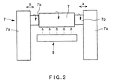
図2は、上記の成膜材料Tの回転装置7と加熱装置8とを説明するための図である。図2において、回転装置7は駆動基部7a,7aと、各駆動基部7aから回転可能に突設された一対の回転アーム7b、7bを備えており、駆動基部7a,7aは矢印方向aに離接するように移動可能であり、回転アーム7b、7bは同軸上で回転可能である。そして、駆動基部7a,7aを移動させることにより、成膜材料T(図示例では、円柱形状をなしている)を回転アーム7b、7b間に挟持して装着することができる。この状態で回転アーム7b、7bを同方向に回転させることにより、成膜材料Tを回転することができる。このような回転アーム7b、7bによる成膜材料Tの回転軸は、成膜材料Tに照射されるプラズマビームに対して80〜100°の範囲の角度をなすように設定する。また、加熱装置8は、回転装置7に挟持され回転している成膜材料Tを外部から加熱するものであり、成膜材料Tの下方近傍に配設されている。この加熱装置8としては、通電加熱ヒーター等の抵抗加熱体や赤外線ランプ等を用いることができる。
【0010】
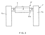
また、図3は、成膜材料Tの回転装置と加熱装置の他の例を説明するための図である。図3において、回転装置7′は駆動基部7′a,7′aを備え、加熱装置8′は円筒状の抵抗加熱体8′aを有し、この抵抗加熱体8′aは駆動基部7′a,7′aの図示しない回転係合部の間に架設することにより回転可能とされる。また、駆動基部7′a,7′aには、架設された抵抗加熱体8aに通電するための配線(図示せず)が配設されている。そして、円筒形状に成形された成膜材料Tの中空部に円筒状の抵抗加熱体8′aを挿入し、抵抗加熱体8′aの両端部を駆動基部7′a,7′aの図示しない回転係合部間に架設して成膜材料Tを装着することにより、成膜材料Tは回転可能なものとなる。このような成膜材料Tの回転軸は、成膜材料Tに照射されるプラズマビームに対して80〜100°の範囲の度をなすように設定する。また、抵抗加熱体8′aに通電することにより、成膜材料Tを内部から加熱することができる。抵抗加熱体8′aとしては、タングステン、タンタル、モリブデン、プラチナ等の高融点材料を用いて成形することができる。また、抵抗加熱体8′aは、上記のような抵抗加熱材料を他の材料で成形した円筒形状体中に配設したものであってもよい。尚、抵抗加熱体8′aの形状は円筒形状の他に棒形状等であってもよい。
【0011】
上記のような本発明のイオンプレーティング装置1では、加熱装置8によって成膜材料Tを加熱することができ、これにより成膜材料T中に含有されている水分を除去することができる。また、圧力勾配型プラズマガン10で発生したプラズマビームは収束用コイル11により収束され、シート化磁石12とアノード磁石9で形成されている磁界に導かれて成膜材料Tに照射される。そして、成膜材料Tは照射されるプラズマビームに対して80〜100°の範囲の角度をなす回転軸で回転装置7によって回転されるため、プラズマビームに均一に曝され、蒸発による減少が均一となって、プラズマビームが照射される面は常に整面状態となる。
【0012】
次に、上述のような本発明のイオンプレーティング装置1を用いた成膜方法について説明する。
まず、回転装置7に装着した成膜材料Tを加熱装置8によって加熱して、成膜材料Tに含有されている水分を除去する。加熱装置8による成膜材料Tの加熱温度は、水分を蒸発除去する温度、例えば、120〜150℃程度に設定することが好ましい。この成膜材料Tの加熱は、回転装置7により成膜材料Tを回転させながら行うことが好ましい。使用する成膜材料Tとしては、酸化珪素(SiOx(1≦x≦2))、酸化マグネシウム、酸化インジウムスズ(ITO)、窒化珪素(SixNy)窒化酸化珪素(SixOyNz)等を挙げることができる。また、成膜材料Tとして、導電性材料を10重量%以下の範囲で含有したものを使用することにより、プラズマガンによる蒸発材料の蒸発が容易になり好ましい。成膜材料Tに含有させる導電性材料としては、B(ボロン)、P(リン)等を挙げることができる。添加回転装置7による成膜材料Tの回転速度は、例えば、0.5〜50rpm程度の範囲で設定することができる。
【0013】
次に、真空排気口6,14からチャンバー2内の空気を排出して所定の到達真空度まで減圧し、次いで、反応ガス供給口15から成膜チャンバー2B内に所定の反応ガスを導入し、チャンバー2内を所定の圧力に保ち、被成膜体Sを走行させる。次に、回転装置7により成膜材料Tを回転させている状態で、アルゴンガス等の不活性ガスを導入した圧力勾配型プラズマガン10にプラズマ生成のための電力を投入し、アノード磁石9の上方近傍に位置する成膜材料Tにプラズマビームを収束させて照射することにより成膜材料を蒸発させる。これにより、成膜材料の蒸発分子が高密度プラズマによりイオン化し、被成膜体S上に付着して薄膜が形成される。
【0014】
このような成膜方法では、プラズマビームによる成膜材料Tの蒸発開始前に、予め成膜材料Tの水分が除去されているので、プラズマビーム照射開始から成膜材料Tの蒸発開始までの時間を短いものとすることができ、また、蒸発を継続させるために圧力勾配型プラズマガン10に投入する電力パワーを増大させる必要がない。さらに、圧力勾配型プラズマガン10から照射されるプラズマビーム内で回転される成膜材料Tは、プラズマビームに均一に曝されるため、蒸発による減少が均一となり、プラズマビームが照射される面は常に整面状態であり、これにより成膜材料Tの蒸発後の飛翔方向が安定し、被成膜体への成膜性が安定したものとなる。また、回転装置が図2に示されるような成膜材料Tを挟持する構造であっても、成膜材料Tの局部的な減少が防止されるので、使用途中での成膜材料Tの割れ、破壊等が大幅に低減され、成膜材料Tの有効利用が可能となる。
尚、本発明は、上述の各実施形態に限定されるものではない。
【0015】
【実施例】
次に、実施例を示して本発明を更に詳細に説明する。
[実施例]
本発明のイオンプレーティング装置として、図1に示すような圧力勾配型プラズマガンを備えた巻取り式のホローカソード型イオンプレーティング装置を準備した。このイオンプレーティング装置は、図2に示されるように、成膜材料を挟持した状態で回転させる回転装置と、回転中の成膜材料を下方近傍から加熱するための抵抗加熱装置とを備えたものとした。そして、回転装置に成膜材料として90%の焼結密度を有する円柱形状(直径200mm、長さ400mm)の一酸化珪素(SiO)を装着した。
【0016】
次に、回転装置に装着した成膜材料を2rpmの回転速度で回転させながら、加熱装置によって成膜材料の温度が120℃となるような加熱処理(15分間)を施した。尚、成膜材料の加熱処理前の水分含有量は1重量%であり、加熱処理後の水分含有量は0.5重量%以下であった。
次いで、被成膜体として幅30cmの巻取り状の2軸延伸ポリエチレンテレフタレートフィルム(東洋紡績(株)製 PETフィルムA4100、厚み100μm、)を準備し、この基材フィルムのコロナ未処理面側を被成膜面として被成膜体搬送チャンバー内に装着した。尚、この基材フィルムと成膜材料との距離(TS距離)は約60cmに設定した。
次に、成膜時の添加ガスとして酸素ガス(大陽東洋酸素(株)製(純度99.9995%以上))、窒素ガス(大陽東洋酸素(株)製(純度99.9999%以上))、および、アルゴンガス(大陽東洋酸素(株)製(純度99.9999%以上))を準備した。
【0017】
次に、チャンバー内を到達真空度5.0×10⁻⁵Paまで減圧した。次いで、成膜チャンバー内に窒素ガスを流量200sccmで、酸素ガスを流量10sccmでそれぞれ導入するとともに、チャンバー内圧力を0.1Paに保ち、基材フィルムを走行させ、アルゴンガスを流量15sccmで導入した圧力勾配型プラズマガンにプラズマ生成のための電力を10kW投入し、アノード磁石の上方近傍で回転している成膜材料にプラズマビームを収束させて照射した。このプラズマビームは成膜材料の回転軸に対して約90°の角度で照射されるものとした。このようなプラズマビームの照射開始から約20分後に回転状態の成膜材料からの蒸発が始まった。その後、回転状態の成膜材料の蒸発を継続させ、高密度プラズマにより蒸発分子をイオン化させて、基材フィルム上に酸化窒化珪素膜からなるバリア層を形成して、バリアフィルムを得た。基材フィルムの走行速度は、成膜開始時点で形成される酸化窒化珪素膜の膜厚が100nmとなるように設定した。尚、sccmとは、standard cubic centimeter per minuteの略であり、以下の比較例においても同様である。
【0018】
このような酸化窒化珪素膜の成膜を100mの基材フィルムに連続して行った後の成膜材料は、直径が約130mmとなるまで減少していたが、外観は整面を備えた円柱形状であった。
【0019】
また、上記の連続成膜の最終部位であるバリアフィルムについて、酸化窒化珪素膜の厚みを測定した結果、約100nmであり、成膜直後と同等の成膜性が維持されていることが確認された。さらに、このバリアフィルムについて、下記の条件で酸素透過率および水蒸気透過率を測定した。その結果、酸素透過率が0.3cc/m2/day・atm以下であり、水蒸気透過率が0.1g/m2/day以下であり、優れたバリア性を有することが確認された。
【0020】
酸素透過率の測定
酸素ガス透過率測定装置(MOCON社製 OX−TRAN 2/20)を用いて、温度23℃、湿度90%RH、バックグラウンド除去測定を行うインディヴィジュアルゼロ(Individual Zero)測定ありの条件で測定した。
水蒸気透過率の測定
水蒸気透過率測定装置(MOCON社製 PERMATRAN−W 3/31)を用いて、温度40℃、湿度100%RHで測定した。
【0021】
[比較例1]
成膜材料に加熱処理を施さず、また、成膜材料を回転させない他は、実施例と同様にして、バリアフィルムを作製した。
このバリアフィルム作製では、プラズマビーム照射開始から成膜材料の蒸発開始まで約40分を要した。また、基材フィルムに対して55mの連続成膜を行った時点で成膜材料が割れて脱落し、成膜が不能となった。そして、連続成膜の最終部位であるバリアフィルムについて、酸化窒化珪素膜の厚みを測定した結果、約70nmであり、成膜直後に比べて成膜性が低下していることが確認された。また、このバリアフィルムについて、実施例と同様に酸素透過率および水蒸気透過率を測定した結果、酸素透過率が2.3cc/m2/day・atmであり、水蒸気透過率が6.0g/m2/dayであり、実施例に比べてバリア性が劣ることが確認された。
【0022】
[比較例2]
実施例におけるホローカソード型イオンプレーティング装置において、回転装置および加熱装置の代わりに坩堝を配設し、この坩堝中に加熱処理を施していない成膜材料(水分含有量は1重量%)を載置した。その後、実施例と同様にして成膜材料にプラズマビームを収束させて照射し、バリアフィルムを作製した。
このバリアフィルム作製では、プラズマビーム照射開始から成膜材料の蒸発開始まで約30分を要した。また、連続成膜の最終部位であるバリアフィルムについて、酸化窒化珪素膜の厚みを測定した結果、約85nmであり、成膜直後に比べて成膜性が低下していることが確認された。また、このバリアフィルムについて、実施例と同様に酸素透過率および水蒸気透過率を測定した。その結果、酸素透過率が1.2cc/m2/day・atmであり、水蒸気透過率が0.9g/m2/dayであり、実施例に比べてバリア性が劣ることが確認された。
【0023】
【発明の効果】
以上詳述したように、本発明によれば加熱手段によって成膜材料が加熱されて含有水分が除去されるので、プラズマガンによる成膜材料の蒸発時の水分の悪影響が排除され、蒸発が開始するまでの時間を短いものとすることができ、かつ、プラズマガンの電力パワーの増大を不要とすることができる。また、プラズマガンから照射されるプラズマビーム内で回転される成膜材料は、プラズマビームに均一に曝されるため、蒸発による減少が均一となり、プラズマビームが照射される面は常に整面状態であり、これにより成膜材料の蒸発後の飛翔方向が安定し、被成膜体への成膜性が安定したものとなる。さらに、上述のように成膜材料の局部的な減少が防止されるので、成膜材料を挟持した状態で使用する場合であっても、使用途中での成膜材料の割れ等が生じ難くなり、成膜材料の有効利用が可能となる。
【図面の簡単な説明】
【図1】本発明のイオンプレーティング装置の一実施形態の構成を示す図面である。
【図2】成膜材料の回転装置と加熱装置とを説明するための図である。
【図3】成膜材料の回転装置と加熱装置の他の例を説明するための図である。
【符号の説明】
1…イオンプレーティング装置
2…真空チャンバー
7,7′…回転装置
7a,7′a…駆動基部
7b…回転アーム
8,8′…加熱装置
8′a…抵抗加熱体
10…プラズマガン
S…被成膜体
T…成膜材料[0001]
TECHNICAL FIELD OF THE INVENTION
The present invention relates to an ion plating apparatus capable of forming a stable and uniform film, and a film forming method using the same.
[0002]
[Prior art]
[Patent Document 1] Japanese Patent Application Laid-Open No. 2000-144390 Japanese Patent Laid-Open Publication No. 2000-144390 A plasma beam generated by a plasma gun is converged and drawn into a vacuum chamber, and this plasma beam is irradiated on a film forming material by a magnetic field to evaporate the film forming material. Conventionally, an ion plating apparatus that forms a thin film by being ionized when passing through the above-described plasma beam and colliding with a film-forming object has been conventionally used. Such an ion plating apparatus has an advantage that a film forming material can be evaporated and ionized by a plasma gun, and that the formed thin film has high adhesion strength.
[0003]
[Problems to be solved by the invention]
However, for example, a sintered body of an inorganic material such as silicon oxide used as a film-forming material of an ion plating apparatus easily absorbs moisture, and a film-forming material provided in a vacuum chamber absorbs moisture. In the case of absorption, there are problems that the time until the start of evaporation by the plasma gun becomes longer and that the power supplied to the plasma gun needs to be increased.
Further, in a conventional ion plating apparatus, since a plasma beam is irradiated to a film forming material from a certain direction, only a portion or a surface to which the plasma beam is applied is partially reduced, and the plasma beam is irradiated as the film forming material evaporates. The surface of the film-forming material hit by the surface becomes rough and irregular. For this reason, there is also a problem that the variation in the flying direction of the evaporated film-forming material becomes large and the film-forming property is reduced.
[0004]
Furthermore, when the film-forming material is used in a sandwiched state, a part of the film-forming material is irradiated with the plasma beam from a certain direction as described above. There is also a problem in that the film-forming material is dropped and the utilization efficiency of the film-forming material is reduced.
The present invention has been made in view of such circumstances, and has an ion plating apparatus capable of stably evaporating a film forming material, forming a uniform film, and effectively using the film forming material. It is another object of the present invention to provide a film forming method using the same.
[0005]
[Means for Solving the Problems]
In order to achieve such an object, an ion plating apparatus of the present invention includes a vacuum chamber in which a film-forming target is disposed, a plasma gun, and a film-forming material disposed in the vacuum chamber. The apparatus is configured to include at least a rotating device for rotating in a plasma beam irradiated from the plasma gun and a heating unit for heating a film-forming material.
As a preferred embodiment of the present invention, the rotating device is configured to rotate the film-forming material on an axis forming an angle in a range of 80 to 100 ° with respect to a plasma beam applied to the film-forming material. .
As a preferred embodiment of the present invention, the rotating device includes a pair of holding members rotatable coaxially in a state where the film forming material is held, and the heating unit is configured to rotate the film forming material held by the holding member. The configuration was such that it was arranged to heat from the outside.
[0006]
As a preferred embodiment of the present invention, the rotating device has a rod-shaped body or a cylindrical body that can hold a film-forming material on a peripheral surface and is rotatable around an axial direction, and the rod-shaped body and the cylindrical body are The resistance heating element was formed, or the resistance heating element was provided.
Further, the present invention provides a film forming method using any one of the above ion plating apparatuses, wherein a step of heating the film forming material by the heating means to remove moisture contained in the film forming material, A step of irradiating the film-forming material with a plasma beam from the plasma gun and evaporating the film-forming material while the film-forming material is rotated by the rotating device to form a thin film on the film-forming target.
In a preferred embodiment of the present invention, the film forming material is configured to use a material containing a conductive material in a range of 10% by weight or less.
[0007]
In the present invention, since the moisture contained in the film-forming material is removed by the heating means, and the film-forming material is exposed to the plasma beam irradiated from the plasma gun while being rotated by the rotating device, The film forming material is uniformly reduced without any irregular surface.
[0008]
BEST MODE FOR CARRYING OUT THE INVENTION
Next, embodiments of the present invention will be described with reference to the drawings.
FIG. 1 is a drawing showing the configuration of an embodiment of the ion plating apparatus of the present invention. In FIG. 1, an
[0009]
FIG. 2 is a diagram for explaining the
[0010]
FIG. 3 is a diagram for explaining another example of a rotating device and a heating device for the film forming material T. In FIG. 3, the rotating device 7 'has driving bases 7'a, 7'a, and the heating device 8' has a cylindrical resistance heating element 8'a, which is connected to the driving base 7 '. 'A, 7'a is rotatable by being bridged between rotation engaging portions (not shown). Wiring (not shown) for supplying electricity to the installed resistance heating element 8a is provided on the driving bases 7'a and 7'a. Then, a cylindrical resistance heating element 8'a is inserted into a hollow portion of the film-forming material T formed into a cylindrical shape, and both ends of the resistance heating element 8'a are illustrated by driving bases 7'a and 7'a. The film-forming material T is rotatable by mounting the film-forming material T between the rotation engaging portions not to be mounted. The rotation axis of such a film forming material T is set so as to make a degree in the range of 80 to 100 ° with respect to the plasma beam irradiated on the film forming material T. Further, by supplying a current to the resistance heating element 8'a, the film-forming material T can be heated from the inside. The resistance heating element 8'a can be formed using a high melting point material such as tungsten, tantalum, molybdenum, and platinum. Further, the resistance heating body 8'a may be one in which the above-described resistance heating material is disposed in a cylindrical body formed of another material. The shape of the resistance heating element 8'a may be a rod shape or the like in addition to the cylindrical shape.
[0011]
In the
[0012]
Next, a film forming method using the above-described
First, the film forming material T mounted on the
[0013]
Next, the air in the
[0014]
In such a film forming method, since the moisture of the film forming material T is removed before the evaporation of the film forming material T by the plasma beam, the time from the start of the plasma beam irradiation to the start of the evaporation of the film forming material T is increased. Can be shortened, and there is no need to increase the power supplied to the pressure
Note that the present invention is not limited to the above embodiments.
[0015]
【Example】
Next, the present invention will be described in more detail with reference to examples.
[Example]
As an ion plating apparatus of the present invention, a winding hollow cathode type ion plating apparatus equipped with a pressure gradient plasma gun as shown in FIG. 1 was prepared. As shown in FIG. 2, the ion plating apparatus includes a rotating device for rotating the film-forming material while holding the film-forming material therebetween, and a resistance heating device for heating the rotating film-forming material from near below. It was taken. Then, a cylindrical (diameter 200 mm, length 400 mm) silicon monoxide (SiO) having a sintering density of 90% was mounted as a film forming material on a rotating device.
[0016]
Next, while rotating the film-forming material mounted on the rotating device at a rotation speed of 2 rpm, a heating treatment was performed by the heating device so that the temperature of the film-forming material became 120 ° C. (15 minutes). The water content of the film-forming material before the heat treatment was 1% by weight, and the water content after the heat treatment was 0.5% by weight or less.
Next, a rolled biaxially stretched polyethylene terephthalate film (PET film A4100 manufactured by Toyobo Co., Ltd., thickness 100 μm) having a width of 30 cm was prepared as a film-forming body, and the corona-untreated surface side of the base film was prepared. It was mounted in a film-forming body transfer chamber as a film-forming surface. The distance (TS distance) between the base film and the film-forming material was set to about 60 cm.
Next, oxygen gas (manufactured by Taiyo Toyo Oxygen Co., Ltd. (purity: 99.9995% or more)) and nitrogen gas (manufactured by Taiyo Toyo Oxygen Co., Ltd. (purity: 99.9999% or more)) are used as additive gases during film formation. ) And argon gas (manufactured by Taiyo Toyo Oxygen Co., Ltd. (purity: 99.9999% or more)).
[0017]
Next, the pressure in the chamber was reduced to the ultimate degree of vacuum of 5.0 × 10 −5 Pa. Next, nitrogen gas was introduced into the film formation chamber at a flow rate of 200 sccm, and oxygen gas was introduced at a flow rate of 10 sccm, while the pressure in the chamber was kept at 0.1 Pa, the substrate film was run, and argon gas was introduced at a flow rate of 15 sccm. An electric power for plasma generation was applied to the pressure gradient type plasma gun at 10 kW, and a plasma beam was converged and irradiated onto the film forming material rotating near and above the anode magnet. This plasma beam was applied at an angle of about 90 ° with respect to the rotation axis of the film-forming material. About 20 minutes after the start of the plasma beam irradiation, evaporation from the rotating film-forming material started. After that, the evaporation of the film-forming material in the rotating state was continued, the evaporated molecules were ionized by high-density plasma, and a barrier layer made of a silicon oxynitride film was formed on the base film to obtain a barrier film. The traveling speed of the base film was set so that the thickness of the silicon oxynitride film formed at the start of film formation was 100 nm. Note that sccm is an abbreviation for standard cubic centimeter per minute, and is the same in the following comparative examples.
[0018]
After such a silicon oxynitride film was continuously formed on a 100-m substrate film, the film-forming material was reduced to a diameter of about 130 mm. It was a shape.
[0019]
Further, the thickness of the silicon oxynitride film was measured for the barrier film, which is the final part of the above continuous film formation, and was found to be about 100 nm, indicating that the same film formability as that immediately after film formation was maintained. Was. Further, the oxygen permeability and the water vapor permeability of the barrier film were measured under the following conditions. As a result, the oxygen permeability was 0.3 cc / m 2 / day · atm or less, and the water vapor permeability was 0.1 g / m 2 / day or less, and it was confirmed that the composition had excellent barrier properties.
[0020]
Measurement of oxygen permeability Using an oxygen gas permeability measuring device (OX-
Measurement of water vapor transmission rate The water vapor transmission rate was measured at a temperature of 40 ° C and a humidity of 100% RH using a water vapor transmission rate measuring apparatus (PERMATRAN-
[0021]
[Comparative Example 1]
A barrier film was produced in the same manner as in the example except that the heat treatment was not performed on the film forming material and the film forming material was not rotated.
In this barrier film preparation, it took about 40 minutes from the start of plasma beam irradiation to the start of evaporation of the film-forming material. Further, when a 55 m continuous film was formed on the substrate film, the film-forming material was cracked and dropped off, and the film could not be formed. Then, the thickness of the silicon oxynitride film was measured for the barrier film, which is the final part of the continuous film formation, and was found to be about 70 nm, indicating that the film formability was lower than immediately after the film formation. Further, as a result of measuring the oxygen permeability and the water vapor permeability of this barrier film in the same manner as in the example, the oxygen permeability was 2.3 cc / m 2 / day · atm, and the water vapor permeability was 6.0 g /
[0022]
[Comparative Example 2]
In the hollow cathode type ion plating apparatus of the embodiment, a crucible is provided instead of the rotating apparatus and the heating apparatus, and a film-forming material (water content is 1% by weight) which is not subjected to the heat treatment is placed in the crucible. Was placed. Thereafter, in the same manner as in the example, a plasma beam was converged and irradiated on the film-forming material to produce a barrier film.
In this barrier film fabrication, it took about 30 minutes from the start of plasma beam irradiation to the start of evaporation of the film-forming material. Further, the thickness of the silicon oxynitride film of the barrier film which was the last part of the continuous film formation was measured to be about 85 nm, and it was confirmed that the film formability was lower than that immediately after the film formation. The oxygen permeability and the water vapor permeability of this barrier film were measured in the same manner as in the example. As a result, the oxygen transmission rate was 1.2 cc / m 2 / day · atm, and the water vapor transmission rate was 0.9 g / m 2 / day, and it was confirmed that the barrier properties were inferior to the examples.
[0023]
【The invention's effect】
As described in detail above, according to the present invention, since the film-forming material is heated by the heating means to remove the contained water, the adverse effect of water when the film-forming material is evaporated by the plasma gun is eliminated, and the evaporation starts. It is possible to shorten the time required to perform the operation, and it is not necessary to increase the power of the plasma gun. In addition, since the film-forming material rotated in the plasma beam irradiated from the plasma gun is uniformly exposed to the plasma beam, the reduction by evaporation becomes uniform, and the surface irradiated with the plasma beam is always in a uniform state. In this case, the flying direction of the film-forming material after evaporation is stabilized, and the film-forming property on the film-forming object becomes stable. Further, since the local decrease of the film-forming material is prevented as described above, even when the film-forming material is used in a sandwiched state, cracking of the film-forming material during use is less likely to occur. Thus, the film forming material can be effectively used.
[Brief description of the drawings]
FIG. 1 is a drawing showing a configuration of an embodiment of an ion plating apparatus of the present invention.
FIG. 2 is a diagram for explaining a film forming material rotating device and a heating device.
FIG. 3 is a view for explaining another example of a rotating device and a heating device of a film forming material.
[Explanation of symbols]
DESCRIPTION OF
Claims (6)
前記加熱手段により成膜材料を加熱して該成膜材料中に含有される水分を除去する工程と、前記回転装置により成膜材料を回転させながら、前記プラズマガンから成膜材料にプラズマビームを照射し蒸発させて被成膜体に薄膜を形成する工程と、を有することを特徴とするイオンプレーティング装置を用いた成膜方法。A film forming method using the ion plating apparatus according to any one of claims 1 to 4,
Heating the film-forming material by the heating means to remove moisture contained in the film-forming material; and, while rotating the film-forming material by the rotating device, applying a plasma beam from the plasma gun to the film-forming material. A step of irradiating and evaporating to form a thin film on a film-forming object, the method comprising using an ion plating apparatus.
Priority Applications (1)
| Application Number | Priority Date | Filing Date | Title |
|---|---|---|---|
| JP2003030520A JP4486308B2 (en) | 2003-02-07 | 2003-02-07 | Ion plating apparatus and film forming method using the same |
Applications Claiming Priority (1)
| Application Number | Priority Date | Filing Date | Title |
|---|---|---|---|
| JP2003030520A JP4486308B2 (en) | 2003-02-07 | 2003-02-07 | Ion plating apparatus and film forming method using the same |
Publications (2)
| Publication Number | Publication Date |
|---|---|
| JP2004238701A true JP2004238701A (en) | 2004-08-26 |
| JP4486308B2 JP4486308B2 (en) | 2010-06-23 |
Family
ID=32957390
Family Applications (1)
| Application Number | Title | Priority Date | Filing Date |
|---|---|---|---|
| JP2003030520A Expired - Fee Related JP4486308B2 (en) | 2003-02-07 | 2003-02-07 | Ion plating apparatus and film forming method using the same |
Country Status (1)
| Country | Link |
|---|---|
| JP (1) | JP4486308B2 (en) |
Cited By (2)
| Publication number | Priority date | Publication date | Assignee | Title |
|---|---|---|---|---|
| JP2009143759A (en) * | 2007-12-13 | 2009-07-02 | Dainippon Printing Co Ltd | Raw material powder of evaporation source material for ion plating, evaporation source material for ion plating and its manufacturing method and gas barrier sheet and its manufacturing method |
| JP2009280832A (en) * | 2008-05-19 | 2009-12-03 | Dainippon Printing Co Ltd | Raw powder for ion plating evaporation source material, ion plating evaporation source material and method for producing the same, gas barrier sheet and method for producing the same |
Citations (2)
| Publication number | Priority date | Publication date | Assignee | Title |
|---|---|---|---|---|
| JPS60194067A (en) * | 1984-03-16 | 1985-10-02 | Agency Of Ind Science & Technol | Formation of hard film |
| JPH0313571A (en) * | 1989-06-12 | 1991-01-22 | Hitachi Ltd | Vapor deposition device, vaporization source and formation of thin film |
-
2003
- 2003-02-07 JP JP2003030520A patent/JP4486308B2/en not_active Expired - Fee Related
Patent Citations (2)
| Publication number | Priority date | Publication date | Assignee | Title |
|---|---|---|---|---|
| JPS60194067A (en) * | 1984-03-16 | 1985-10-02 | Agency Of Ind Science & Technol | Formation of hard film |
| JPH0313571A (en) * | 1989-06-12 | 1991-01-22 | Hitachi Ltd | Vapor deposition device, vaporization source and formation of thin film |
Cited By (2)
| Publication number | Priority date | Publication date | Assignee | Title |
|---|---|---|---|---|
| JP2009143759A (en) * | 2007-12-13 | 2009-07-02 | Dainippon Printing Co Ltd | Raw material powder of evaporation source material for ion plating, evaporation source material for ion plating and its manufacturing method and gas barrier sheet and its manufacturing method |
| JP2009280832A (en) * | 2008-05-19 | 2009-12-03 | Dainippon Printing Co Ltd | Raw powder for ion plating evaporation source material, ion plating evaporation source material and method for producing the same, gas barrier sheet and method for producing the same |
Also Published As
| Publication number | Publication date |
|---|---|
| JP4486308B2 (en) | 2010-06-23 |
Similar Documents
| Publication | Publication Date | Title |
|---|---|---|
| JP4747802B2 (en) | Vacuum film forming method and vacuum film forming apparatus | |
| KR100736664B1 (en) | Substrate with ITO transparent conductive film and method for producing same | |
| JP2009108381A (en) | Film-forming apparatus and film-forming method | |
| EP2762605B1 (en) | Film formation method and film formation apparatus | |
| TWI397595B (en) | Evaporation system | |
| JP4167833B2 (en) | Film forming apparatus, oxide thin film forming substrate and manufacturing method thereof | |
| JP4486308B2 (en) | Ion plating apparatus and film forming method using the same | |
| WO2004042110A1 (en) | Method of forming film on substrate | |
| US20190164775A1 (en) | Etching method and etching apparatus | |
| JP2001262323A (en) | Film deposition method and system | |
| JP6987172B2 (en) | Etching method and etching equipment | |
| JPH08209329A (en) | Winding-up vapor-deposition device and cvd device | |
| JPH09165674A (en) | Vacuum coating apparatus | |
| JP2009043613A (en) | Pulsed electron beam generating device, and pulsed electron beam film deposition device | |
| JP2000128528A (en) | Production of superconducting thin film | |
| JP2012214831A (en) | Vacuum film deposition apparatus | |
| JP4649789B2 (en) | Barrier laminate | |
| JPH07166335A (en) | Ion plating device | |
| JPH05230630A (en) | Formation of thin film | |
| JP2003301260A (en) | Winding type electron beam vacuum vapor deposition device | |
| WO1987005637A1 (en) | Continuous ion plating device for rapidly moving film | |
| JPH0860360A (en) | Production of optical thin film and apparatus for production therefor | |
| JPH08225927A (en) | Crucible for evaporation | |
| JPH0196372A (en) | Ion plating apparatus | |
| JPH06264227A (en) | Ion plating device |
Legal Events
| Date | Code | Title | Description |
|---|---|---|---|
| A621 | Written request for application examination |
Free format text: JAPANESE INTERMEDIATE CODE: A621 Effective date: 20060127 |
|
| A977 | Report on retrieval |
Free format text: JAPANESE INTERMEDIATE CODE: A971007 Effective date: 20080812 |
|
| A131 | Notification of reasons for refusal |
Free format text: JAPANESE INTERMEDIATE CODE: A131 Effective date: 20080819 |
|
| A521 | Written amendment |
Free format text: JAPANESE INTERMEDIATE CODE: A523 Effective date: 20080924 |
|
| A131 | Notification of reasons for refusal |
Free format text: JAPANESE INTERMEDIATE CODE: A131 Effective date: 20090915 |
|
| A521 | Written amendment |
Free format text: JAPANESE INTERMEDIATE CODE: A523 Effective date: 20091105 |
|
| TRDD | Decision of grant or rejection written | ||
| A01 | Written decision to grant a patent or to grant a registration (utility model) |
Free format text: JAPANESE INTERMEDIATE CODE: A01 Effective date: 20100316 |
|
| A01 | Written decision to grant a patent or to grant a registration (utility model) |
Free format text: JAPANESE INTERMEDIATE CODE: A01 |
|
| A61 | First payment of annual fees (during grant procedure) |
Free format text: JAPANESE INTERMEDIATE CODE: A61 Effective date: 20100326 |
|
| R150 | Certificate of patent (=grant) or registration of utility model |
Free format text: JAPANESE INTERMEDIATE CODE: R150 |
|
| FPAY | Renewal fee payment (prs date is renewal date of database) |
Free format text: PAYMENT UNTIL: 20130402 Year of fee payment: 3 |
|
| FPAY | Renewal fee payment (prs date is renewal date of database) |
Free format text: PAYMENT UNTIL: 20140402 Year of fee payment: 4 |
|
| LAPS | Cancellation because of no payment of annual fees |