JP2004234792A - Head slider, head gimbals assembly and hard disc device - Google Patents
Head slider, head gimbals assembly and hard disc device Download PDFInfo
- Publication number
- JP2004234792A JP2004234792A JP2003024621A JP2003024621A JP2004234792A JP 2004234792 A JP2004234792 A JP 2004234792A JP 2003024621 A JP2003024621 A JP 2003024621A JP 2003024621 A JP2003024621 A JP 2003024621A JP 2004234792 A JP2004234792 A JP 2004234792A
- Authority
- JP
- Japan
- Prior art keywords
- heater
- electrode pad
- head
- wiring
- electrode pads
- Prior art date
- Legal status (The legal status is an assumption and is not a legal conclusion. Google has not performed a legal analysis and makes no representation as to the accuracy of the status listed.)
- Granted
Links
Images


Classifications
-
- G—PHYSICS
- G11—INFORMATION STORAGE
- G11B—INFORMATION STORAGE BASED ON RELATIVE MOVEMENT BETWEEN RECORD CARRIER AND TRANSDUCER
- G11B5/00—Recording by magnetisation or demagnetisation of a record carrier; Reproducing by magnetic means; Record carriers therefor
- G11B5/48—Disposition or mounting of heads or head supports relative to record carriers ; arrangements of heads, e.g. for scanning the record carrier to increase the relative speed
- G11B5/4806—Disposition or mounting of heads or head supports relative to record carriers ; arrangements of heads, e.g. for scanning the record carrier to increase the relative speed specially adapted for disk drive assemblies, e.g. assembly prior to operation, hard or flexible disk drives
- G11B5/4853—Constructional details of the electrical connection between head and arm
-
- G—PHYSICS
- G11—INFORMATION STORAGE
- G11B—INFORMATION STORAGE BASED ON RELATIVE MOVEMENT BETWEEN RECORD CARRIER AND TRANSDUCER
- G11B5/00—Recording by magnetisation or demagnetisation of a record carrier; Reproducing by magnetic means; Record carriers therefor
- G11B5/48—Disposition or mounting of heads or head supports relative to record carriers ; arrangements of heads, e.g. for scanning the record carrier to increase the relative speed
- G11B5/58—Disposition or mounting of heads or head supports relative to record carriers ; arrangements of heads, e.g. for scanning the record carrier to increase the relative speed with provision for moving the head for the purpose of maintaining alignment of the head relative to the record carrier during transducing operation, e.g. to compensate for surface irregularities of the latter or for track following
- G11B5/60—Fluid-dynamic spacing of heads from record-carriers
- G11B5/6005—Specially adapted for spacing from a rotating disc using a fluid cushion
- G11B5/6011—Control of flying height
- G11B5/6064—Control of flying height using air pressure
Landscapes
- Magnetic Heads (AREA)
- Adjustment Of The Magnetic Head Position Track Following On Tapes (AREA)
Abstract
Description
【0001】
【発明の属する技術分野】
本発明は、磁気抵抗効果素子と誘導型電磁変換素子とを備えた薄膜磁気ヘッドを有するヘッドスライダ、ヘッドジンバルアセンブリ及びハードディスク装置に関する。
【0002】
【従来の技術】
一般に、ヘッドジンバルアセンブリは、薄膜磁気ヘッドが形成されたヘッドスライダをサスペンションに接続されたジンバルに搭載して構成される。ヘッドスライダにおけるジンバルの先端側に位置する面には、薄膜磁気ヘッドに備えられた再生用の磁気抵抗効果素子と書込用の誘導型電磁変換素子とに通電するための複数の電極パッドが設けられている(例えば、特許文献1参照。)。
【0003】
上記の電極パッドには、電気信号を入出力するための配線の一端が接続されている。この配線は、ヘッドスライダの周囲のジンバル上を這ってサスペンションの基端まで伸長しており、他端が磁気ディスクドライブ装置の信号端子に接続されている。再生用の磁気抵抗効果素子の配線には、一定の電流(センス電流)が常時供給されている。
【0004】
【特許文献1】
特開平8−111015号公報
【0005】
【発明が解決しようとする課題】
しかしながら、上記従来のヘッドジンバルアセンブリでは、磁気抵抗効果素子の配線と誘導型電磁変換素子の配線とがジンバル上で並列に這わされているため、誘導型電磁変換素子の配線に電流を供給した場合、磁気抵抗効果素子の配線にノイズが乗る現象、すなわちクロストークを引き起こしてしまう虞がある。
【0006】
本発明の目的は、磁気抵抗効果素子の配線と誘導型電磁変換素子の配線との間におけるクロストークを防止することができるヘッドスライダ、ヘッドジンバルアセンブリ及びハードディスク装置を提供することである。
【0007】
【課題を解決するための手段】
本発明のヘッドスライダは、再生用の磁気抵抗効果素子と、書込用の誘導型電磁変換素子と、通電されることにより発熱するヒータと、を備えた薄膜磁気ヘッドを有し、磁気抵抗効果素子に通電するための第1素子用電極パッドと、誘導型電磁変換素子に通電するための第2素子用電極パッドと、ヒータに通電するためのヒータ用電極パッドとを同一面に備え、ヒータ用電極パッドは、第1及び第2素子用電極パッドの群の両側に位置していることを特徴とするものである。
【0008】
本発明のヘッドスライダは、同一面内において、ヒータ用電極パッドが、磁気抵抗効果素子用の第1素子用電極パッド及び誘導型電磁変換素子用の第2素子用電極パッドよりも外側に配されている。これらの電極パッドに接続される配線は、電極パッドが備えられた面から折り返されてヘッドスライダの周囲を回り込み、ヘッドスライダの後方へと這わされる。この際、2本のヒータの配線がスライダを挟むようにする。従って、ヒータ用電極パッドに接続された配線は、第1素子用電極パッドに接続された配線と第2誘導素子用電極パッドに接続された配線との間に位置することとなる。これにより、誘導型電磁変換素子の配線と磁気抵抗効果素子の配線との間がヒータの配線によって隔てられるため、誘導型電磁変換素子の配線に電流が供給された場合でも、磁気抵抗効果素子の配線へのクロストークを防止することができる。
【0009】
本発明は、薄膜磁気ヘッドが形成されたヘッドスライダと、ヘッドスライダが搭載されるアームとを備えたヘッドジンバルアセンブリであって、薄膜磁気ヘッドは、再生用の磁気抵抗効果素子と、書込用の誘導型電磁変換素子と、通電されることにより発熱するヒータと、を備え、ヘッドスライダは、磁気抵抗効果素子に通電するための第1素子用電極パッドと、誘導型電磁変換素子に通電するための第2素子用電極パッドと、ヒータに通電するためのヒータ用電極パッドとを同一面に備え、ヒータ用電極パッドは、第1及び第2素子用電極パッドの群の両側に位置していることを特徴とするものである。
【0010】
また、本発明のヘッドジンバルアセンブリでは、第1素子用電極パッド、第2素子用電極パッド及びヒータ用電極パッドに接続される通電用の配線は、電極パッドが備えられた面から折り返され、ヘッドスライダの周囲を回り込んでアームの基端側へ伸長しており、電極パッドが備えられた面とアームの基端との間の領域において、ヒータ用電極パッドの配線が、第1素子用電極パッドの配線と第2素子用電極パッドの配線との間に位置していることを特徴としている。
【0011】
本発明のヘッドジンバルアセンブリでは、ヘッドスライダの同一面内において、ヒータ用電極パッドが、磁気抵抗効果素子用の第1素子用電極パッド及び誘導型電磁変換素子用の第2素子用電極パッドよりも外側に配されている。これらの電極パッドに接続される配線は、アームの先端側から折り返されてヘッドスライダの周囲を回り込み、アームの基端側へと這わされる。この際、2本のヒータの配線がスライダを挟むようにする。従って、ヒータ用電極パッドに接続された配線は、第1素子用電極パッドに接続された配線と第2誘導素子用電極パッドに接続された配線との間に位置することとなる。これにより、誘導型電磁変換素子の配線と磁気抵抗効果素子の配線との間がヒータの配線によって隔てられるため、誘導型電磁変換素子の配線に電流が供給された場合でも、磁気抵抗効果素子の配線へのクロストークを防止することができる。
【0012】
本発明は、薄膜磁気ヘッドが形成されたヘッドスライダと、ヘッドスライダが搭載されるアームとを備えたヘッドジンバルアセンブリを有するハードディスク装置であって、薄膜磁気ヘッドは、再生用の磁気抵抗効果素子と、書込用の誘導型電磁変換素子と、通電されることにより発熱するヒータと、を備え、ヘッドスライダは、磁気抵抗効果素子に通電するための第1素子用電極パッドと、誘導型電磁変換素子に通電するための第2素子用電極パッドと、ヒータに通電するためのヒータ用電極パッドとを同一面に備え、ヒータ用電極パッドは、第1及び第2素子用電極パッドの群の両側に位置していることを特徴とするものである。
【0013】
また、本発明のハードディスク装置では、第1素子用電極パッド、第2素子用電極パッド及びヒータ用電極パッドに接続される通電用の配線は、電極パッドが備えられた面から折り返され、ヘッドスライダの周囲を回り込んでアームの基端側へ伸長しており、電極パッドが備えられた面とアームの基端との間の領域において、ヒータ用電極パッドの配線が、第1素子用電極パッドの配線と第2素子用電極パッドの配線との間に位置していることを特徴としている。
【0014】
本発明のハードディスク装置では、ヘッドスライダの同一面内において、ヒータ用電極パッドが、磁気抵抗効果素子用の第1素子用電極パッド及び誘導型電磁変換素子用の第2素子用電極パッドよりも外側に配されている。これらの電極パッドに接続される配線は、アームの先端側から折り返されてヘッドスライダの周囲を回り込み、アームの基端側へと這わされる。この際、2本のヒータの配線がスライダを挟むようにする。従って、ヒータ用電極パッドに接続された配線は、第1素子用電極パッドに接続された配線と第2素子用電極パッドに接続された配線との間に位置することとなる。これにより、誘導型電磁変換素子の配線と磁気抵抗効果素子の配線との間がヒータの配線によって隔てられるため、誘導型電磁変換素子の配線に電流が供給された場合でも、磁気抵抗効果素子の配線へのクロストークを防止することができる。
【0015】
【発明の実施の形態】
以下、図面を参照して、本発明の好適な実施形態について詳細に説明する。尚、同一要素には同一符号を用いるものとし、重複する説明は省略する。
【0016】
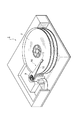
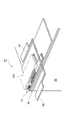
図1は、本実施形態のヘッドスライダを備えたハードディスク装置を示す図であり、図2は、図1に示すハードディスク装置に備えられ、薄膜磁気ヘッドが形成されたヘッドスライダを搭載したヘッドジンバルアセンブリの拡大斜視図である。ハードディスク装置1は、ヘッドジンバルアセンブリ(HGA:Head Gimbals Assembly)10を作動させて、高速回転するハードディスク2の記録面(図1の上面)に、薄膜磁気ヘッド11によって磁気情報を記録及び再生するものである。
【0017】
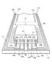
図2に示すように、ヘッドジンバルアセンブリ10は、金属製の薄板であるサスペンションアーム12を備えている。サスペンションアーム12の先端側には、切込みで囲われたタング部14が形成されており、このタング部14上に薄膜磁気ヘッド11が形成されたヘッドスライダ13が搭載されている。
【0018】
また、サスペンションアーム12上には、先端側に設けられた端子15a〜15fと基端側に設けられた端子16a〜16fとに接続される配線17a〜17cを絶縁層で被覆したプリント配線17が備えられている。配線17a〜17cは、順に、後述するヒータ用電極パッド23a,23b、記録用電極パッド21a,21b、再生用電極パッド22a,22bに電気的に接続される(図3参照)。
【0019】
プリント配線17は、端子15a〜15fからヘッドスライダ13の周囲を回り込んでヘッドスライダ13の後方へと這わされ、端子16a〜16fまで伸長している。このプリント配線17によって、ヘッドスライダ13に形成された薄膜磁気ヘッド11の各素子が端子15a〜15fを介して通電されるようになっている。
【0020】
尚、ヘッドスライダ13、プリント配線17及び各端子15a〜15f,16a〜16fは、絶縁層18を介してサスペンションアーム12上に配されており、金属製のサスペンションアーム12とは絶縁されている。
【0021】
以上のようなヘッドジンバルアセンブリ10は、図1に示すように、支軸3周りに例えばボイスコイルモータによって回転可能となっている。ヘッドジンバルアセンブリ10を回転させると、ヘッドスライダ13は、ハードディスク2の半径方向、すなわちトラックラインを横切る方向に移動する。
【0022】
図3は、図2に示すヘッドスライダ13の拡大図である。ヘッドスライダ13は、略直方体形状をなし、アルティック(Al2O3・TiC)からなる基台20上に、薄膜磁気ヘッド11が形成されている。尚、図では、薄膜磁気ヘッド11が、基台20の水平方向における中央付近に形成されているが、形成位置はこれには限定されない。
【0023】
図3におけるヘッドスライダ13の上面は、ハードディスク2の記録面に対向する記録媒体対向面であり、エアベアリング面(ABS:Air Bearing Surface)Sと称される。ハードディスク2が回転する際、この回転に伴う空気流によってヘッドスライダ13が浮上し、エアベアリング面Sはハードディスク2の記録面から離隔する。尚、エアベアリング面Sは、DLC(Diamond Like Carbon)等のコーティングが施されていてもよい。
【0024】
図3におけるヘッドスライダ13の手前側の面には、薄膜磁気ヘッド11を保護するために、オーバーコート層21が設けられている。オーバーコート層21の表面には、記録用電極パッド21a,21b、再生用電極パッド22a,22b及びヒータ用電極パッド23a,23bが取り付けられている。ヒータ用電極パッド23a,23bは、記録用電極パッド21a,21b及び再生用電極パッド22a,22bからなる群の両側に位置している。ヒータの詳細は後述する。尚、図では、記録用電極パッド21a,21bの右側に再生用電極パッド22a,22bが取り付けられているが、左右反対に取り付けられていてもよい。
【0025】
記録用電極パッド21a,21b、再生用電極パッド22a,22b及びヒータ用電極パッド23a,23bは、サスペンションアーム12に設けられた端子15a〜15fにそれぞれ電気的に接続されている。本実施形態では、記録用電極パッド21a,21bがそれぞれ端子15e,15fに、再生用電極パッド22a,22bがそれぞれ端子15a,15bに、ヒータ用電極パッド23a,23bがそれぞれ端子15d,15cに電気的に接続されている。
【0026】
各電極パッドと端子15a〜15fとの接続に際しては、例えば、ボンディングの材質として金を用いたボールボンディング(ゴールドボールボンディング;Gold Ball Bonding)が用いられる。
【0027】
更に、端子15a〜15fには、上述した配線17a〜17cが接続されている。本実施形態において、記録用電極パッド21a,21bに電気的に接続された配線17b,17bは、ヒータ用電極パッド23aに電気的に接続された配線17aと共に、各電極パッドが備えられた面から折り返されてヘッドスライダ13の周囲を回り込み、図2に示す端子16e,16fに接続される。この場合、配線17aは、端子16dに接続される。再生用電極パッド22a,22bに電気的に接続された配線17c,17cは、ヒータ用電極パッド23bに電気的に接続された配線17aと共に、配線17b,17bとは反対の方向に折り返されてヘッドスライダ13の周囲を回り込み、図2に示す端子16a,16bに接続される。この場合、配線17aは、端子16cに接続される。
【0028】
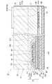
図4は、薄膜磁気ヘッド11におけるエアベアリング面Sに対して垂直な方向の概略断面図である。薄膜磁気ヘッド11は、基台20上に、再生用のGMR素子(磁気抵抗効果素子;Giant Magneto Resistive)30を有する再生ヘッド部31と、書込用の誘導型の電磁変換素子としての記録ヘッド部32とを積層した複合型薄膜磁気ヘッドとなっている。GMR素子は、磁気抵抗変化率が高い巨大磁気抵抗効果を利用したものである。
【0029】
記録ヘッド部32は、いわゆる面内記録方式を採用しており、下部磁極33と、GMR素子30との間に下部磁極33を挟むとともに下部磁極33に磁気的に連結された上部磁極34と、一部が下部磁極33と上部磁極34との間に位置する薄膜コイル35とを主として備えている。
【0030】
上部磁極34は、エアベアリング面S側に位置する磁極部分層34aと、これに接続されると共に薄膜コイル35の上方を迂回するヨーク部分層34bとから構成されている。
【0031】
また、GMR素子30におけるエアベアリング面Sとは反対側、すなわちエアベアリング面Sから見たGMR素子30の裏側には、Cu,NiFe,Ta,Ti,CoNiFe合金,FeAlSi合金等で形成されたヒータ40aが設けられている。このヒータ40aは、通電による発熱で周囲の層を熱膨張させ、GMR素子30とハードディスク2との間隔を調整するものである。
【0032】
ヒータ40aは、蛇行形状をしており、その両端には図中上方に伸びたCu等の導電材料からなる2つの導電部41a,41bが電気的に接続されている。該導電部41a,41bの上端(オーバーコート層21の表面)にはそれぞれ上述したヒータ用電極パッド23a,23bが取り付けられている。
【0033】
また同様に、再生ヘッド部31及び記録ヘッド部32に関しても、導電材料からなる2つの導電部(図示せず)が電気的に接続されており、導電部の上端において、それぞれ上述した再生用電極パッド22a,22b、記録用電極パッド21a,21bに接続されている。
【0034】
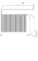
図5は、ヒータ40aの一例を示す平面図である。ヒータ40aは、一本のラインを蛇行させた構造となっており、ラインの両端にはそれぞれ引出し電極85a,85bが接続されている。引出し電極85a,85bは、それぞれ図4に示した導電部41a,41bに接続されている。
【0035】
ヒータ40aの寸法については、例えば蛇行させるラインのピッチを3μmとし、ライン幅を2μm、隣り合うラインの間隔を1μmとする。ヒータ用電極パッド23a,23b間に電圧を印加してヒータ40aに通電することで(例えば20mA程度の電流を流す)、ヒータ40aが発熱するようになっている。
【0036】
尚、導電部41a,41b、ヒータ用電極パッド23a,23b、記録用電極パッド21a,21b及び再生用電極パッド22a,22bは、図4の紙面に対し垂直な方向に並設されているため、図4では、ヒータ40aにおける導電部41a及びヒータ用電極パッド23aについてのみを示している。
【0037】
以上のように構成されたヘッドスライダ13は、図3に示すように、同一面内において、ヒータ用電極パッド23a,23bが、記録用電極パッド21a,21b及び再生用電極パッド22a,22bよりも外側に配されている。
【0038】
これらの電極パッドに接続される配線17a〜17cは、サスペンションアーム12の先端側から折り返されてヘッドスライダ13の周囲を回り込み、サスペンションアーム12の基端側へと這わされている。
【0039】
このため、プリント配線17のうち、ヒータ用電極パッド23a,23bに電気的に接続された配線17aは、各電極パッドが備えられた面とサスペンションアーム12の基端との間の領域において、記録用電極パッド21a,21bに電気的に接続された一対の配線17bと再生用電極パッド22a,22bに電気的に接続された一対の配線17cとの間に位置することとなる。
【0040】
従って、記録ヘッド部32の配線17bと再生ヘッド部31の配線17cとの間がヒータ40aの配線17aによって隔てられることとなり、記録ヘッド部32の配線17bに電流が供給された場合でも、再生ヘッド部31の配線17cにノイズが乗ることはなく、すなわちクロストークが防止される。
【0041】
ここで、図4に示した薄膜磁気ヘッドの製造方法の一例を説明する。
【0042】
まず、アルティック(Al2O3・TiC)等からなる基板38に、スパッタリング法によって、例えばアルミナ(Al2O3)等の絶縁材料からなる下地層39を厚さ約1μm〜約10μmで形成する。基板38及び下地層39は、後にヘッドスライダの基台20となるものである。
【0043】
次に、下部シールド層42上に、公知の手法によってGMR素子30を形成する。GMR素子30は、実際は複数の膜から構成されるが、図においては単層で示している。次に、下部シールド層42及びGMR素子30を覆うように、例えばスパッタリング法によってAl2O3等からなる絶縁層44を形成する。尚、図4において、ここで積層された絶縁層と、下部シールド層42とを一体的に絶縁層44として示している。
【0044】
続いて、GMR素子30及び絶縁層44を覆うように、例えばめっき法によって上部シールド層45を厚さ約1.0μm〜約4.0μmで形成する。また、上部シールド層45を形成するのと同時に、同じく絶縁層44上に、上部シールド層45の作製と同一の処理(例えばめっき法)によってCu,NiFe,Ta,Ti,CoNiFe合金,FeAlSi合金等の導電性材料からなるヒータ40aを形成する。ヒータ40aの高さは、例えば上部シールド層45と同程度にする。上部シールド層45とヒータ40aを同一の材料にする場合は、両者を同時に形成できる。
【0045】
次に、上部シールド層45及びヒータ40a上に、例えばスパッタリング法によって、Al2O3等の絶縁材料からなる絶縁層46をヒータ40aが覆われる程度に厚く積層する。その後、この絶縁層46の表面を研磨して平坦にする。このとき、絶縁層46は、上部シールド層45上での厚さが約0.1μm〜約0.5μmであり、上部シールド層45の後方ではそれより厚くなっている。以上により、再生ヘッド部31が得られる。尚、絶縁層46を始めから約0.1μm〜約0.5μmで積層してもよく、この場合、絶縁層46を積層し、ヒータ40aの絶縁層46から突出した部分を覆うように、後述するオーバーコート層21を形成する。
【0046】
次いで、絶縁層46上に、パーマロイからなる下部磁極33を例えばスパッタリング法で形成する。そして、下部磁極33上に例えばスパッタリング法で非磁性層50を形成し、この非磁性層50上にフォトレジスト層51を形成する。また、非磁性層50には、フォトリソグラフィ及びドライエッチングによってコンタクトホール50hを形成する。
【0047】
更に、フォトレジスト層51上に、フォトリソグラフィ及びめっき法等を利用して一段目の薄膜コイル35を厚さ約1μm〜約3μmで形成した後、薄膜コイル35上にフォトレジスト層53を形成する。薄膜コイル35の一部は、下部磁極33と上部磁極34との間に位置する。
【0048】
1段目の薄膜コイル35を形成した後に、上部磁極34の磁極部分層34aを形成し、その後2段目の薄膜コイル35を形成する。その後、薄膜コイル35の中央部に相当する位置において非磁性層50をエッチングすることでコンタクトホール50hを形成し、上部磁極34の後側部分となるヨーク部分層34bを形成する。本実施形態では薄膜コイル35及びフォトレジスト層53は2段積層するが、段数や形成手順はこれに限られない。
【0049】
次に、上部磁極34を覆うように、オーバーコート層21を形成する。尚、図4に示した導電部41a,41bは、概略以下の手法により形成することができる。すなわち、ヒータ40a及び引出し電極85a,85b(図5参照)を形成した後に、引出し電極85a,85bがその後の積層材料で覆われないようにレジストパターンを形成する。そして、例えばオーバーコート層21を形成した後に、このレジストパターンをリフトオフする。次いで、例えばフレームめっき法によって導電部41a,41bを形成し、これらの上端部にヒータ用電極パッド23a,23bを配設する。
【0050】
また、再生ヘッド部31及び記録ヘッド部32に関しても、ヒータ40aと同様に導電部を形成し、図3に示すように、記録用電極パッド21a,21b及び再生用電極パッド22a,22bを、ヒータ用電極パッド23a,23bと共にヘッドスライダ13の同一面上に配設する。
【0051】
以上により、記録ヘッド部32が得られ、本実施形態の薄膜磁気ヘッド11が完成する。
【0052】
ここで、ヒータの設置位置の他の形態について説明する。
【0053】
図6は、ヒータの設置位置の他の形態を示す図である。同図に示すように、ヒータは、例えば、基板38とGMR素子30との間に位置する層に設けてもよいし(図6中の二点鎖線で示すヒータ40b)、記録ヘッド部32の上方に設けてもよい(図6中の二点鎖線で示すヒータ40c)。
【0054】
ヒータ40cの位置にヒータを設ける場合は、まず、オーバーコート層21の上にヒータ40cを形成し、次いで、例えばスパッタリング法によって、Al2O3等の絶縁材料からなるオーバーコート層52を更に形成する。
【0055】
また、ヒータは、上述した位置に一つだけ配置してもよいし、2つに分割して配置してもよい。図7は、ヒータが分割して配置された薄膜磁気ヘッド11の一例を示す概略断面図である。同図において、分割配置されたヒータ60は、図6に示すオーバーコート層52内に設けられたヒータ40cと同じ高さ位置に配されている。同図では、ヒータ40cの高さ位置での分割配置を示しているが、図6に示すヒータ40a,40bの高さ位置で分割配置してももちろんよく、高さ位置は限定されない。
【0056】
上述したようにして薄膜磁気ヘッド11が完成したとき、薄膜磁気ヘッド11は、一枚の基板38上に複数形成された状態となっている。この状態から図3に示すヘッドスライダ13を得るためには、まず、基板38を切断して薄膜磁気ヘッド11が列状に配置された複数本のバーとし、更に、そのバーを切断して、それぞれが薄膜磁気ヘッド11を有するブロック単位に切断する。その後、所望のスライダレールを形成し(図示せず)、イオンミリング等を施し、ヘッドスライダ13が完成する。
【0057】
また、このヘッドスライダ13をサスペンションアーム12の先端側に搭載し、ヘッドスライダ13に電気的に接続する配線17a〜17cをサスペンションアーム12上に這わせ、配線17a〜17cの一端をサスペンションアーム12の先端側に設けられた端子15a〜15fにボンディングし、他端をサスペンションアーム12の基端側に設けられた端子16a〜16fにボンディングすることによってヘッドジンバルアセンブリ10を作製することができる。ヘッドジンバルアセンブリ10を作製した後、ヘッドスライダ13がハードディスク2上を移動可能で、且つ、磁気信号の記録及び再生が可能となるように組み立てることで、図1に示したハードディスク装置1が完成する。
【0058】
以上、本発明を実施形態に基づき具体的に説明したが、本発明は上記実施形態に限定されるものではない。例えば、第2の磁極を磁極部分層とヨーク部分層とに分けず、一体にしてもよい。また、薄膜磁気ヘッドを面内記録方式ではなく、垂直記録方式としてもよい。更に、再生ヘッド部において、GMR素子の代わりに、異方性磁気抵抗効果を利用するAMR(Anisotropy Magneto Resistive)素子、トンネル接合で生じる磁気抵抗効果を利用するTMR(Tunnel−type Magneto Resistive)素子等を利用してもよい。
【0059】
【発明の効果】
本発明によれば、ヘッドスライダの同一面内において、ヒータ用電極パッドが第1及び第2素子用電極パッドの群の両側に位置しているため、磁気抵抗効果素子の配線と誘導型電磁変換素子の配線との間におけるクロストークを防止することができる。
【図面の簡単な説明】
【図1】実施形態に係るヘッドスライダを備えたハードディスク装置を示す図である。
【図2】図1に示すハードディスク装置に備えられ、薄膜磁気ヘッドが形成されたヘッドスライダを搭載したヘッドジンバルアセンブリを示す拡大斜視図である。
【図3】図2に示すヘッドスライダの拡大図である。
【図4】薄膜磁気ヘッドにおけるエアベアリング面に対して垂直な方向の概略断面図である。
【図5】ヒータ40aの一例を示す平面図である。
【図6】ヒータの設置位置の他の形態を示す図である。
【図7】ヒータが分割して配置された薄膜磁気ヘッドの一例を示す概略断面図である。
【符号の説明】
1…ハードディスク装置、2…ハードディスク、3…支軸、10…ヘッドジンバルアセンブリ、11…薄膜磁気ヘッド、12…サスペンションアーム、13…ヘッドスライダ、14…タング部、15a〜15f,16a〜16f…端子、17…プリント配線、17a,17b,17c…配線、18…絶縁層、20…基台、21…オーバーコート層、21a,21b…記録用電極パッド(第2素子用電極パッド)、22a,22b…再生用電極パッド(第1素子用電極パッド)、23a,23b…ヒータ用電極パッド、31…再生ヘッド部、32…記録ヘッド部、33…下部磁極、34…上部磁極、34a…磁極部分層、34b…ヨーク部分層、35…薄膜コイル、38…基板、39…下地層、40a,40b,40c…ヒータ、41a,41b…導電部、42…下部シールド層、44…絶縁層、45…上部シールド層、46…絶縁層、50h…コンタクトホール、50…非磁性層、51…フォトレジスト層、52…オーバーコート層、53…フォトレジスト層、60…ヒータ、85a,85b…引出し電極、S…エアベアリング面(記録媒体対向面)。[0001]
TECHNICAL FIELD OF THE INVENTION
The present invention relates to a head slider, a head gimbal assembly, and a hard disk drive having a thin-film magnetic head including a magnetoresistive element and an inductive electromagnetic transducer.
[0002]
[Prior art]
Generally, a head gimbal assembly is configured by mounting a head slider on which a thin-film magnetic head is formed on a gimbal connected to a suspension. A plurality of electrode pads are provided on a surface of the head slider located on the leading end side of the gimbal for supplying current to the reproducing magnetoresistive effect element and the writing inductive electromagnetic transducer provided in the thin-film magnetic head. (See, for example, Patent Document 1).
[0003]
One end of a wiring for inputting and outputting an electric signal is connected to the electrode pad. The wiring extends along the gimbal around the head slider to the base end of the suspension, and the other end is connected to a signal terminal of the magnetic disk drive. A constant current (sense current) is constantly supplied to the wiring of the magnetoresistive element for reproduction.
[0004]
[Patent Document 1]
JP-A-8-111015
[0005]
[Problems to be solved by the invention]
However, in the above-mentioned conventional head gimbal assembly, since the wiring of the magnetoresistive effect element and the wiring of the inductive electromagnetic transducer are laid in parallel on the gimbal, when current is supplied to the wiring of the inductive electromagnetic transducer. In addition, there is a possibility that a noise may occur on the wiring of the magnetoresistive effect element, that is, crosstalk may be caused.
[0006]
An object of the present invention is to provide a head slider, a head gimbal assembly, and a hard disk device that can prevent crosstalk between wiring of a magnetoresistive element and wiring of an inductive electromagnetic transducer.
[0007]
[Means for Solving the Problems]
A head slider according to the present invention includes a thin-film magnetic head including a magnetoresistive element for reproduction, an inductive electromagnetic transducer for writing, and a heater that generates heat when energized, and has a magnetoresistive effect. A first element electrode pad for energizing the element, a second element electrode pad for energizing the inductive electromagnetic transducer, and a heater electrode pad for energizing the heater are provided on the same surface; The electrode pads for the first and second elements are located on both sides of the group of the electrode pads for the first and second elements.
[0008]
In the head slider of the present invention, the heater electrode pad is disposed outside the first element electrode pad for the magnetoresistive effect element and the second element electrode pad for the inductive electromagnetic transducer in the same plane. ing. The wirings connected to these electrode pads are folded back from the surface on which the electrode pads are provided, wrap around the head slider, and crawl behind the head slider. At this time, the wires of the two heaters sandwich the slider. Therefore, the wiring connected to the heater electrode pad is located between the wiring connected to the first element electrode pad and the wiring connected to the second inductive element electrode pad. Accordingly, the wiring of the inductive type electromagnetic transducer is separated from the wiring of the magnetoresistive element by the wiring of the heater. Crosstalk to wiring can be prevented.
[0009]
The present invention relates to a head gimbal assembly including a head slider on which a thin-film magnetic head is formed, and an arm on which the head slider is mounted, wherein the thin-film magnetic head comprises a magnetoresistive element for reproduction, The head slider includes a first element electrode pad for supplying current to the magnetoresistive element, and a power supply for the induction type electromagnetic transducer. Element electrode pads for supplying power to the heater and heater electrode pads for supplying electricity to the heater are provided on the same surface, and the heater electrode pads are located on both sides of the first and second element electrode pads. It is characterized by having.
[0010]
In the head gimbal assembly according to the present invention, the current supply wiring connected to the first element electrode pad, the second element electrode pad, and the heater electrode pad is folded back from the surface on which the electrode pad is provided, and The wire of the heater electrode pad extends around the slider and extends toward the base end of the arm, and in a region between the surface on which the electrode pad is provided and the base end of the arm, the first element electrode It is characterized in that it is located between the wiring of the pad and the wiring of the electrode pad for the second element.
[0011]
In the head gimbal assembly according to the present invention, the heater electrode pad is larger than the first element electrode pad for the magnetoresistive element and the second element electrode pad for the inductive electromagnetic conversion element in the same plane of the head slider. It is arranged outside. The wiring connected to these electrode pads is folded from the distal end side of the arm, goes around the head slider, and crawls to the base end side of the arm. At this time, the wires of the two heaters sandwich the slider. Therefore, the wiring connected to the heater electrode pad is located between the wiring connected to the first element electrode pad and the wiring connected to the second inductive element electrode pad. Thus, the wiring of the induction type electromagnetic transducer is separated from the wiring of the magnetoresistive element by the wiring of the heater. Therefore, even when a current is supplied to the wiring of the induction type electromagnetic transducer, the wiring of the magnetoresistive element is not affected. Crosstalk to wiring can be prevented.
[0012]
The present invention is a hard disk drive having a head gimbal assembly including a head slider on which a thin-film magnetic head is formed, and an arm on which the head slider is mounted, wherein the thin-film magnetic head has a magnetoresistive element for reproduction and An inductive electromagnetic transducer for writing, and a heater that generates heat when energized, wherein the head slider includes a first element electrode pad for energizing the magnetoresistive element, and an inductive electromagnetic transducer. A second element electrode pad for energizing the element and a heater electrode pad for energizing the heater are provided on the same surface, and the heater electrode pads are disposed on both sides of the first and second element electrode pads. Is characterized in that
[0013]
Further, in the hard disk drive of the present invention, the current supply wiring connected to the first element electrode pad, the second element electrode pad, and the heater electrode pad is folded back from the surface provided with the electrode pad, and the head slider is provided. And the wiring of the heater electrode pad is provided in the region between the surface provided with the electrode pad and the base end of the arm. And the wiring of the second element electrode pad.
[0014]
In the hard disk drive of the present invention, the heater electrode pad is located outside the first element electrode pad for the magnetoresistive effect element and the second element electrode pad for the inductive electromagnetic conversion element in the same plane of the head slider. It is arranged in. The wiring connected to these electrode pads is folded from the distal end side of the arm, goes around the head slider, and crawls to the base end side of the arm. At this time, the wires of the two heaters sandwich the slider. Therefore, the wiring connected to the heater electrode pad is located between the wiring connected to the first element electrode pad and the wiring connected to the second element electrode pad. Thus, the wiring of the induction type electromagnetic transducer is separated from the wiring of the magnetoresistive element by the wiring of the heater. Therefore, even when a current is supplied to the wiring of the induction type electromagnetic transducer, the wiring of the magnetoresistive element is not affected. Crosstalk to wiring can be prevented.
[0015]
BEST MODE FOR CARRYING OUT THE INVENTION
Hereinafter, preferred embodiments of the present invention will be described in detail with reference to the drawings. In addition, the same reference numerals are used for the same elements, and redundant description will be omitted.
[0016]
FIG. 1 is a diagram showing a hard disk drive provided with a head slider according to the present embodiment. FIG. 2 is a head gimbal assembly mounted on the hard disk drive shown in FIG. 1 and mounted with a head slider formed with a thin-film magnetic head. It is an expansion perspective view of. The
[0017]
As shown in FIG. 2, the
[0018]
On the
[0019]
The printed
[0020]
The
[0021]
As shown in FIG. 1, the
[0022]
FIG. 3 is an enlarged view of the
[0023]
The upper surface of the
[0024]
An
[0025]
The
[0026]
For connection between each electrode pad and the
[0027]
Further, the above-described
[0028]
FIG. 4 is a schematic sectional view of the thin-film
[0029]
The
[0030]
The upper
[0031]
Further, a heater formed of Cu, NiFe, Ta, Ti, CoNiFe alloy, FeAlSi alloy, or the like on the opposite side of the
[0032]
The
[0033]
Similarly, also with respect to the reproducing
[0034]
FIG. 5 is a plan view illustrating an example of the
[0035]
Regarding the dimensions of the
[0036]
Since the
[0037]
As shown in FIG. 3, in the
[0038]
The
[0039]
For this reason, of the printed
[0040]
Therefore, the
[0041]
Here, an example of a method for manufacturing the thin-film magnetic head shown in FIG. 4 will be described.
[0042]
First, Altic (Al 2 O 3 A substrate 38 made of TiC) or the like, for example, alumina (Al 2 O 3 ) Is formed with a thickness of about 1 μm to about 10 μm. The
[0043]
Next, the
[0044]
Subsequently, the
[0045]
Next, an Al film is formed on the
[0046]
Next, the lower
[0047]
Further, after forming the first-stage
[0048]
After forming the first-stage thin-
[0049]
Next, the
[0050]
In addition, as for the reproducing
[0051]
As described above, the
[0052]
Here, another configuration of the installation position of the heater will be described.
[0053]
FIG. 6 is a diagram showing another configuration of the installation position of the heater. 6, the heater may be provided, for example, in a layer located between the
[0054]
When providing a heater at the position of the
[0055]
Further, only one heater may be disposed at the above-described position, or the heater may be divided into two. FIG. 7 is a schematic cross-sectional view showing an example of the thin-film
[0056]
When the thin-film
[0057]
The
[0058]
As described above, the present invention has been specifically described based on the embodiments. However, the present invention is not limited to the above embodiments. For example, the second magnetic pole may be integrated without being divided into the magnetic pole partial layer and the yoke partial layer. Further, the thin film magnetic head may be of a perpendicular recording system instead of the in-plane recording system. Further, in the read head, instead of the GMR element, an AMR (Anisotropic Magneto Resistive) element using an anisotropic magnetoresistance effect, a TMR (Tunnel-type Magneto Resistive) element using a magnetoresistance effect generated in a tunnel junction, and the like. May be used.
[0059]
【The invention's effect】
According to the present invention, since the heater electrode pads are located on both sides of the group of the first and second element electrode pads in the same plane of the head slider, the wiring of the magnetoresistive element and the inductive electromagnetic conversion are provided. Crosstalk between the element and the wiring can be prevented.
[Brief description of the drawings]
FIG. 1 is a diagram showing a hard disk drive provided with a head slider according to an embodiment.
2 is an enlarged perspective view showing a head gimbal assembly provided in the hard disk device shown in FIG. 1 and having a head slider on which a thin film magnetic head is formed.
FIG. 3 is an enlarged view of the head slider shown in FIG.
FIG. 4 is a schematic sectional view of a thin-film magnetic head in a direction perpendicular to an air bearing surface.
FIG. 5 is a plan view showing an example of a
FIG. 6 is a view showing another form of the installation position of the heater.
FIG. 7 is a schematic sectional view showing an example of a thin-film magnetic head in which a heater is divided and arranged.
[Explanation of symbols]
DESCRIPTION OF
Claims (5)
前記磁気抵抗効果素子に通電するための第1素子用電極パッドと、前記誘導型電磁変換素子に通電するための第2素子用電極パッドと、前記ヒータに通電するためのヒータ用電極パッドとを同一面に備え、
前記ヒータ用電極パッドは、前記第1及び第2素子用電極パッドの群の両側に位置していることを特徴とするヘッドスライダ。A thin-film magnetic head including a magnetoresistive element for reproduction, an inductive electromagnetic transducer for writing, and a heater that generates heat when energized;
A first element electrode pad for energizing the magnetoresistive effect element, a second element electrode pad for energizing the inductive electromagnetic transducer, and a heater electrode pad for energizing the heater. Prepare for the same side,
The head slider, wherein the heater electrode pads are located on both sides of the group of the first and second element electrode pads.
前記薄膜磁気ヘッドは、再生用の磁気抵抗効果素子と、書込用の誘導型電磁変換素子と、通電されることにより発熱するヒータと、を備え、
前記ヘッドスライダは、前記磁気抵抗効果素子に通電するための第1素子用電極パッドと、前記誘導型電磁変換素子に通電するための第2素子用電極パッドと、前記ヒータに通電するためのヒータ用電極パッドとを同一面に備え、
前記ヒータ用電極パッドは、前記第1及び第2素子用電極パッドの群の両側に位置していることを特徴とするヘッドジンバルアセンブリ。A head gimbal assembly including a head slider on which a thin-film magnetic head is formed, and an arm on which the head slider is mounted,
The thin-film magnetic head includes a magnetoresistive element for reproduction, an inductive electromagnetic transducer for writing, and a heater that generates heat when energized,
The head slider includes a first element electrode pad for energizing the magnetoresistive element, a second element electrode pad for energizing the inductive electromagnetic transducer, and a heater for energizing the heater. And electrode pads for
The head gimbal assembly according to claim 1, wherein the heater electrode pads are located on both sides of the group of the first and second element electrode pads.
前記電極パッドが備えられた面と前記アームの基端との間の領域において、前記ヒータ用電極パッドの配線が、前記第1素子用電極パッドの配線と前記第2素子用電極パッドの配線との間に位置していることを特徴とする請求項2記載のヘッドジンバルアセンブリ。The current supply wiring connected to the first element electrode pad, the second element electrode pad, and the heater electrode pad is folded back from the surface on which the electrode pad is provided, and turns around the head slider. And extends toward the base end of the arm,
In a region between the surface on which the electrode pads are provided and the base end of the arm, the wiring of the heater electrode pad is formed by the wiring of the first element electrode pad and the wiring of the second element electrode pad. 3. The head gimbal assembly according to claim 2, wherein the head gimbal assembly is located between the two.
前記薄膜磁気ヘッドは、再生用の磁気抵抗効果素子と、書込用の誘導型電磁変換素子と、通電されることにより発熱するヒータと、を備え、
前記ヘッドスライダは、前記磁気抵抗効果素子に通電するための第1素子用電極パッドと、前記誘導型電磁変換素子に通電するための第2素子用電極パッドと、前記ヒータに通電するためのヒータ用電極パッドとを同一面に備え、
前記ヒータ用電極パッドは、前記第1及び第2素子用電極パッドの群の両側に位置していることを特徴とするハードディスク装置。A hard disk drive having a head gimbal assembly including a head slider on which a thin film magnetic head is formed, and an arm on which the head slider is mounted,
The thin-film magnetic head includes a magnetoresistive element for reproduction, an inductive electromagnetic transducer for writing, and a heater that generates heat when energized,
The head slider includes a first element electrode pad for energizing the magnetoresistive element, a second element electrode pad for energizing the inductive electromagnetic transducer, and a heater for energizing the heater. And electrode pads for
The hard disk device according to claim 1, wherein the heater electrode pads are located on both sides of the group of the first and second element electrode pads.
前記電極パッドが備えられた面と前記アームの基端との間の領域において、前記ヒータ用電極パッドの配線が、前記第1素子用電極パッドの配線と前記第2素子用電極パッドの配線との間に位置していることを特徴とする請求項4記載のハードディスク装置。The current supply wiring connected to the first element electrode pad, the second element electrode pad, and the heater electrode pad is folded back from the surface on which the electrode pad is provided, and turns around the head slider. And extends toward the base end of the arm,
In a region between the surface on which the electrode pads are provided and the base end of the arm, the wiring of the heater electrode pad is formed by the wiring of the first element electrode pad and the wiring of the second element electrode pad. The hard disk drive according to claim 4, wherein the hard disk drive is located between the two.
Priority Applications (2)
| Application Number | Priority Date | Filing Date | Title |
|---|---|---|---|
| JP2003024621A JP3681376B2 (en) | 2003-01-31 | 2003-01-31 | Head gimbal assembly and hard disk device |
| US10/764,460 US7113369B2 (en) | 2003-01-31 | 2004-01-27 | Head slider, head gimbal assembly, and hard disk drive |
Applications Claiming Priority (1)
| Application Number | Priority Date | Filing Date | Title |
|---|---|---|---|
| JP2003024621A JP3681376B2 (en) | 2003-01-31 | 2003-01-31 | Head gimbal assembly and hard disk device |
Publications (2)
| Publication Number | Publication Date |
|---|---|
| JP2004234792A true JP2004234792A (en) | 2004-08-19 |
| JP3681376B2 JP3681376B2 (en) | 2005-08-10 |
Family
ID=32953105
Family Applications (1)
| Application Number | Title | Priority Date | Filing Date |
|---|---|---|---|
| JP2003024621A Expired - Fee Related JP3681376B2 (en) | 2003-01-31 | 2003-01-31 | Head gimbal assembly and hard disk device |
Country Status (2)
| Country | Link |
|---|---|
| US (1) | US7113369B2 (en) |
| JP (1) | JP3681376B2 (en) |
Cited By (5)
| Publication number | Priority date | Publication date | Assignee | Title |
|---|---|---|---|---|
| JP2006331485A (en) * | 2005-05-24 | 2006-12-07 | Hitachi Global Storage Technologies Netherlands Bv | Magnetic head slider and magnetic head assembly |
| JP2007287191A (en) * | 2006-04-12 | 2007-11-01 | Hitachi Global Storage Technologies Netherlands Bv | Thin film magnetic head |
| JP2008226439A (en) * | 2007-03-13 | 2008-09-25 | Headway Technologies Inc | Recording/reproducing head and its manufacturing method |
| US7633703B2 (en) | 2006-08-18 | 2009-12-15 | Tdk Corporation | Measuring method of flying height and magnetic disk drive apparatus capable of adjusting flying height |
| US7986481B2 (en) | 2006-08-24 | 2011-07-26 | Tdk Corporation | Magnetic reproducing method for suppressing low temperature noise |
Families Citing this family (18)
| Publication number | Priority date | Publication date | Assignee | Title |
|---|---|---|---|---|
| US7086931B2 (en) * | 2003-04-18 | 2006-08-08 | Tdk Corporation | Magnetic head bar holding unit, lapping device, and method of lapping medium-opposing surface of thin-film magnetic head |
| JP3978420B2 (en) * | 2003-10-30 | 2007-09-19 | ヒタチグローバルストレージテクノロジーズネザーランドビーブイ | Magnetic head slider and method for manufacturing magnetic head support mechanism |
| US7187520B2 (en) * | 2004-03-01 | 2007-03-06 | Hitachi Global Storage Technologies Netherlands, B.V. | Magnetic head having thermally assisted recording device, and method of fabrication thereof |
| JP4255869B2 (en) * | 2004-03-24 | 2009-04-15 | ヒタチグローバルストレージテクノロジーズネザーランドビーブイ | Magnetic disk drive and magnetic head slider used therefor |
| US7542243B2 (en) * | 2005-02-18 | 2009-06-02 | Seagate Technology Llc | Slider with transducing and heating elements formed on trailing end thereof and sharing same thin film structure |
| JP2007026591A (en) * | 2005-07-20 | 2007-02-01 | Alps Electric Co Ltd | Thin-film magnetic head |
| JP2007207307A (en) * | 2006-01-31 | 2007-08-16 | Fujitsu Ltd | Flying head slider and recording medium driving apparatus |
| US7948714B2 (en) * | 2006-01-31 | 2011-05-24 | Seagate Technology Llc | Transducer including an element of a transducer and a sidewall in an electrically conductive magnetic layer |
| JP2007335062A (en) * | 2006-05-19 | 2007-12-27 | Alps Electric Co Ltd | Thin film magnetic head |
| US20080023468A1 (en) * | 2006-07-27 | 2008-01-31 | Fujitsu Limited | Magnetic head |
| JP4923295B2 (en) * | 2006-09-13 | 2012-04-25 | 株式会社東芝 | Suspension device |
| US20080218900A1 (en) * | 2007-03-09 | 2008-09-11 | Tdk Corporation | Multi-channel thin-film magnetic head and magnetic tape drive apparatus with the multi-channel thin-film magnetic head |
| US20080253021A1 (en) * | 2007-04-12 | 2008-10-16 | Seagate Technology Llc | Non-magnetic contact enhancement feature |
| US8094418B2 (en) * | 2008-04-02 | 2012-01-10 | Headway Technologies, Inc. | Vertically stacked DFH heater design for protrusion shape control |
| US20100265618A1 (en) * | 2009-04-15 | 2010-10-21 | Zine-Eddine Boutaghou | Method and Apparatus for Reducing Head Media Spacing in a Disk Drive |
| US8760808B2 (en) * | 2010-04-29 | 2014-06-24 | Seagate Technology Llc | Magnetic device containing a heater |
| US9773514B2 (en) * | 2011-02-25 | 2017-09-26 | Headway Technologies, Inc. | Magnetic head for perpendicular magnetic recording that includes a sensor for detecting contact with a recording medium |
| US8760787B2 (en) * | 2011-12-02 | 2014-06-24 | HGST Netherlands B.V. | Magnetic head having a thermal fly-height control (TFC) structure under a flat lower shield |
Family Cites Families (19)
| Publication number | Priority date | Publication date | Assignee | Title |
|---|---|---|---|---|
| US5530604A (en) * | 1994-05-19 | 1996-06-25 | International Business Machines Corporation | Electrical connection and slider-suspension assembly having an improved electrical connection |
| JPH08111015A (en) | 1994-09-01 | 1996-04-30 | Tdk Corp | Supporting device of magnetic head slider and magnetic head device |
| US5889636A (en) * | 1997-06-12 | 1999-03-30 | International Business Machines Corporation | Electrical connection for slider/suspension assembly |
| JP2002260203A (en) * | 2001-03-02 | 2002-09-13 | Tdk Corp | Manufacturing method of thin film magnetic head, and its wafer structure |
| US6813118B2 (en) * | 2002-01-04 | 2004-11-02 | Seagate Technology Llc | Transducing head having improved studs and bond pads to reduce thermal deformation |
| JP3669975B2 (en) * | 2002-06-21 | 2005-07-13 | Tdk株式会社 | Thin film magnetic head |
| JP4076434B2 (en) * | 2002-12-12 | 2008-04-16 | 株式会社日立グローバルストレージテクノロジーズ | Magnetic head and head gimbal assembly |
| JP3632025B2 (en) * | 2003-02-26 | 2005-03-23 | Tdk株式会社 | Thin film magnetic head, head gimbal assembly, and hard disk drive |
| JP3940688B2 (en) * | 2003-03-20 | 2007-07-04 | Tdk株式会社 | Head slider, head gimbal assembly and hard disk device |
| JP4047252B2 (en) * | 2003-06-09 | 2008-02-13 | アルプス電気株式会社 | Method for manufacturing thin film structure |
| JP2005056508A (en) * | 2003-08-05 | 2005-03-03 | Tdk Corp | Method for manufacturing thin film magnetic head |
| JP4433727B2 (en) * | 2003-09-02 | 2010-03-17 | Tdk株式会社 | Flexure, suspension and head gimbal assembly |
| JP3978420B2 (en) * | 2003-10-30 | 2007-09-19 | ヒタチグローバルストレージテクノロジーズネザーランドビーブイ | Magnetic head slider and method for manufacturing magnetic head support mechanism |
| US7027264B1 (en) * | 2003-10-31 | 2006-04-11 | Western Digital Technologies, Inc. | Slider with a slider ground pad electrically connected to write head poles and read head shields |
| JP4255869B2 (en) * | 2004-03-24 | 2009-04-15 | ヒタチグローバルストレージテクノロジーズネザーランドビーブイ | Magnetic disk drive and magnetic head slider used therefor |
| JP4020114B2 (en) * | 2004-10-07 | 2007-12-12 | Tdk株式会社 | Thin-film magnetic head with heating element, head gimbal assembly with thin-film magnetic head, and magnetic disk drive with head gimbal assembly |
| US7495856B2 (en) * | 2004-10-29 | 2009-02-24 | Hitachi Global Storage Technologies Netherlands B.V. | Disk drive slider design for thermal fly-height control and burnishing-on-demand |
| JP2006164414A (en) * | 2004-12-08 | 2006-06-22 | Hitachi Global Storage Technologies Netherlands Bv | Magnetic disk unit |
| JP2006196141A (en) * | 2004-12-13 | 2006-07-27 | Tdk Corp | Thin film magnetic head with heating means, head gimbal assembly with the thin film magnetic head, and magnetic disk device with the head gimbal assembly |
-
2003
- 2003-01-31 JP JP2003024621A patent/JP3681376B2/en not_active Expired - Fee Related
-
2004
- 2004-01-27 US US10/764,460 patent/US7113369B2/en not_active Expired - Lifetime
Cited By (6)
| Publication number | Priority date | Publication date | Assignee | Title |
|---|---|---|---|---|
| JP2006331485A (en) * | 2005-05-24 | 2006-12-07 | Hitachi Global Storage Technologies Netherlands Bv | Magnetic head slider and magnetic head assembly |
| JP2007287191A (en) * | 2006-04-12 | 2007-11-01 | Hitachi Global Storage Technologies Netherlands Bv | Thin film magnetic head |
| US7633703B2 (en) | 2006-08-18 | 2009-12-15 | Tdk Corporation | Measuring method of flying height and magnetic disk drive apparatus capable of adjusting flying height |
| US7986481B2 (en) | 2006-08-24 | 2011-07-26 | Tdk Corporation | Magnetic reproducing method for suppressing low temperature noise |
| JP2008226439A (en) * | 2007-03-13 | 2008-09-25 | Headway Technologies Inc | Recording/reproducing head and its manufacturing method |
| US9659584B2 (en) | 2007-03-13 | 2017-05-23 | Headway Technologies, Inc. | Dynamic flying height read/write head with off-track contact capability at touch down in hard disk drives |
Also Published As
| Publication number | Publication date |
|---|---|
| US20040257706A1 (en) | 2004-12-23 |
| JP3681376B2 (en) | 2005-08-10 |
| US7113369B2 (en) | 2006-09-26 |
Similar Documents
| Publication | Publication Date | Title |
|---|---|---|
| JP3681376B2 (en) | Head gimbal assembly and hard disk device | |
| JP3669975B2 (en) | Thin film magnetic head | |
| JP3940688B2 (en) | Head slider, head gimbal assembly and hard disk device | |
| US7203035B2 (en) | Thin-film magnetic head having a sheet-shaped heater with a lead part connected in series with the heater and having a resistance lower than the heater | |
| JP3636133B2 (en) | Thin film magnetic head, head gimbal assembly including the thin film magnetic head, and magnetic disk apparatus including the head gimbal assembly | |
| JP3632025B2 (en) | Thin film magnetic head, head gimbal assembly, and hard disk drive | |
| US7436633B2 (en) | Thin-film magnetic head, head gimbal assembly and hard disk system | |
| US7102856B2 (en) | Head slider and manufacturing method thereof | |
| JP3626954B2 (en) | Thin-film magnetic head manufacturing method, thin-film magnetic head, head gimbal assembly, and hard disk device | |
| JP2005056509A (en) | Thin-film magnetic head, head gimbals assembly, and hard disk device | |
| US6909584B2 (en) | Magnetic tunnel effect type magnetic head having a magnetic tunnel junction element sandwiched with conductive gap layers between a pair of magnetic shielding layers | |
| US7180707B2 (en) | Thin-film magnetic head, head gimbal assembly, and hard disk drive | |
| JPWO2004051762A1 (en) | Electromagnetic conversion element and CPP structure magnetoresistive effect element | |
| JP2004288352A (en) | Lapping method of surface facing medium for thin film magnetic head | |
| JP2006040447A (en) | Method for manufacturing slider | |
| WO2001003129A1 (en) | Method of manufacturing thin-film magnetic head | |
| JP3975206B2 (en) | Method of lapping of medium facing surface in thin film magnetic head | |
| JP2006196127A (en) | Thin-film magnetic head, magnetic head assembly, and magnetic-disk drive device | |
| JPH08153312A (en) | Magnetic head and magnetic disk device | |
| JP2004022003A (en) | Thin film magnetic head |
Legal Events
| Date | Code | Title | Description |
|---|---|---|---|
| A871 | Explanation of circumstances concerning accelerated examination |
Free format text: JAPANESE INTERMEDIATE CODE: A871 Effective date: 20040827 |
|
| A975 | Report on accelerated examination |
Free format text: JAPANESE INTERMEDIATE CODE: A971005 Effective date: 20040903 |
|
| A131 | Notification of reasons for refusal |
Free format text: JAPANESE INTERMEDIATE CODE: A131 Effective date: 20040907 |
|
| A521 | Written amendment |
Free format text: JAPANESE INTERMEDIATE CODE: A523 Effective date: 20041019 |
|
| A02 | Decision of refusal |
Free format text: JAPANESE INTERMEDIATE CODE: A02 Effective date: 20041207 |
|
| A521 | Written amendment |
Free format text: JAPANESE INTERMEDIATE CODE: A523 Effective date: 20050207 |
|
| A521 | Written amendment |
Free format text: JAPANESE INTERMEDIATE CODE: A523 Effective date: 20050225 |
|
| A911 | Transfer to examiner for re-examination before appeal (zenchi) |
Free format text: JAPANESE INTERMEDIATE CODE: A911 Effective date: 20050330 |
|
| TRDD | Decision of grant or rejection written | ||
| A01 | Written decision to grant a patent or to grant a registration (utility model) |
Free format text: JAPANESE INTERMEDIATE CODE: A01 Effective date: 20050510 |
|
| A61 | First payment of annual fees (during grant procedure) |
Free format text: JAPANESE INTERMEDIATE CODE: A61 Effective date: 20050517 |
|
| R150 | Certificate of patent or registration of utility model |
Ref document number: 3681376 Country of ref document: JP Free format text: JAPANESE INTERMEDIATE CODE: R150 Free format text: JAPANESE INTERMEDIATE CODE: R150 |
|
| FPAY | Renewal fee payment (event date is renewal date of database) |
Free format text: PAYMENT UNTIL: 20080527 Year of fee payment: 3 |
|
| FPAY | Renewal fee payment (event date is renewal date of database) |
Free format text: PAYMENT UNTIL: 20090527 Year of fee payment: 4 |
|
| FPAY | Renewal fee payment (event date is renewal date of database) |
Free format text: PAYMENT UNTIL: 20090527 Year of fee payment: 4 |
|
| FPAY | Renewal fee payment (event date is renewal date of database) |
Free format text: PAYMENT UNTIL: 20100527 Year of fee payment: 5 |
|
| FPAY | Renewal fee payment (event date is renewal date of database) |
Free format text: PAYMENT UNTIL: 20110527 Year of fee payment: 6 |
|
| FPAY | Renewal fee payment (event date is renewal date of database) |
Free format text: PAYMENT UNTIL: 20130527 Year of fee payment: 8 |
|
| FPAY | Renewal fee payment (event date is renewal date of database) |
Free format text: PAYMENT UNTIL: 20140527 Year of fee payment: 9 |
|
| LAPS | Cancellation because of no payment of annual fees |