JP2004233807A - Liquid crystal device and its driving method, and electronic equipment - Google Patents
Liquid crystal device and its driving method, and electronic equipment Download PDFInfo
- Publication number
- JP2004233807A JP2004233807A JP2003024080A JP2003024080A JP2004233807A JP 2004233807 A JP2004233807 A JP 2004233807A JP 2003024080 A JP2003024080 A JP 2003024080A JP 2003024080 A JP2003024080 A JP 2003024080A JP 2004233807 A JP2004233807 A JP 2004233807A
- Authority
- JP
- Japan
- Prior art keywords
- liquid crystal
- polarity
- period
- source
- line
- Prior art date
- Legal status (The legal status is an assumption and is not a legal conclusion. Google has not performed a legal analysis and makes no representation as to the accuracy of the status listed.)
- Withdrawn
Links
Images


Abstract
Description
【0001】
【発明の属する技術分野】
本発明は、縦クロストークを軽減するようにした電圧変調方式の液晶装置及びその駆動方法並びに電子機器に関する。
【0002】
【従来の技術】
電気光学装置、例えば、電気光学物質として液晶を用いた液晶表示装置は、陰極線管(CRT)に代わるディスプレイデバイスとして、各種情報処理機器の表示部や液晶テレビ等に広く用いられている。
【0003】
このような液晶表示装置は、例えば、マトリクス状に配列した画素電極と、この画素電極に接続されたTFT(Thin Film Transistor : 薄膜トランジスタ)のようなスイッチング素子等が設けられた素子基板と、画素電極に対向する対向電極が形成された対向基板と、これら両基板との間に充填された電気光学物質たる液晶とによって構成される。
【0004】
このような構成における液晶表示装置の表示モードには、電圧が加わらない状態で白表示するモードであるノーマリーホワイトと、黒表示するモードであるノーマリーブラックとがある。
【0005】
次に、液晶表示装置において画像を階調表示する動作について説明する。
【0006】
スイッチング素子は走査線(ゲート線)を介して供給される走査信号(ゲート信号)によって導通する。走査信号を印加してスイッチング素子を導通状態にした状態で、データ線(ソース線)を介して画素電極に、階調に応じた電圧の画像信号を印加する。そうすると、画素電極と対向電極に、画像信号の電圧に応じた電荷が蓄積される。電荷蓄積後、走査信号を取り去りスイッチング素子を非導通状態にしても、各電極における電荷の蓄積状態は、液晶層の容量性や蓄積容量等によって維持される。
【0007】
このように、各スイッチング素子を駆動させ、蓄積させる電荷量を階調に応じて制御すると、画素毎に液晶の配向状態が変化して光の透過率が変わり、画素毎に明るさを変化させることができる。こうして、階調表示することが可能となる。
【0008】
液晶層及び蓄積容量の容量性を考慮すると、各画素の液晶層に電荷を印加するのは一部の期間のみでよい。従って、マトリクス状に配設された複数の画素を駆動する場合には、同一走査ラインに接続された画素に各走査線によって同時に走査信号を印加し、画像信号をデータ線を介して各画素に供給し、また画像信号を供給する走査線を順次切換えればよい。即ち、液晶表示装置では、走査線及びデータ線を複数の画素について共通化した時分割マルチプレックス駆動が可能となる。
【0009】
なお、液晶装置では、印加信号の直流成分の印加などによって、例えば、液晶成分の分解、液晶セル中の不純物による汚染が発生し、表示画像の焼き付き等の現象が現れる。そこで、一般的には、各画素電極の駆動電圧の極性を、例えば画像信号におけるフレーム毎に反転させる反転駆動が行われる。フレーム反転駆動等の面反転駆動は、画像表示領域を構成する全画素電極の駆動電圧の極性を全て同じにして、一定周期で駆動電圧を反転させる方式である。
【0010】
上述したように、液晶装置では、容量性を考慮して、画素には一部の期間にのみ駆動電圧が印加される。しかし、駆動電圧が印加されない期間においても、結合容量の影響及び電荷のリークによって、画素に印加される電圧が変化する。このような電位変動によって、特に、中間調領域では画質の劣化が目立ってしまう。
【0011】
図15はこのような問題点を説明するための説明図であり、図16及び図17は図15に対応した液晶駆動電位を説明するための波形図である。図16及び図17のVsはソース線に印加される電位を示し、図16及び図17のVA (実線),VB(1点鎖線)は夫々図中のA点及びB点における画素電極の印加電位を示している。図16は容量結合による縦クロストーク現象を示しており、図17は電流リークによる縦クロストーク現象を示している。
【0012】
いま、画面の中央に矩形の黒を表示すると共に、その他の画面の領域に中間調のグレー表示を表示するための画像信号を液晶パネルに与えるものとする。図15はこの場合における液晶パネルの画面全域の表示を示している。図15に示すように、この場合には、黒表示部分の上方において、本来のグレー表示よりも暗い画像部分が表示され、黒表示部分の下方において、本来のグレー表示よりも明るい画像部分が表示されてしまう。
【0013】
図16及び図17のVsは、このような画像の左右方向の中央、例えば図15の点A,Bを通過する縦線の位置に対応するソース線に印加されるソース電位波形を示している。図16及び図17のNフレームは液晶の正極性駆動時の波形であり、(N+1)フレームは液晶の負極性駆動時の波形である。図15の黒部分の表示に対応する期間T1 ,T2 において、ソース電位は対向電極の電位(対向電位 )との差が大きくなっており、C点等のグレー表示に対応する期間では、対向電位との差が小さくなっている。
【0014】
図16のVA,VBにおいて、期間T1 ,T2 を破線に変えた波形は、縦クロストークが生じていない理想的な画素電極の印加電位波形を示している。第NフレームのA点の画面垂直位置に対応するタイミングt1で、A点の画素のTFTがオンとなってA点の画素電極に中間調のグレー表示に対応したレベルの画像信号(駆動電位)が印加される。A点の次のラインの画素に画像信号が供給されるタイミングでは、A点の画素のTFTはオフであり、A点の画素電極の駆動電位は、液晶容量及び付加容量によって保持される。第N+1フレームにおいてA点の画面垂直位置に対応するタイミングになると、A点の画素には負極性の駆動電位が印加される。この駆動電位も次のN+2フレームまで保持される。B点についても同様であり、B点の画素の画素電極に印加される駆動電位は、液晶容量及び付加容量によって、次のフレームまで保持される。
【0015】
しかしながら、結合容量及び電荷のリークによって、画素電極はTFTがオフの期間においても、ソース線電位の影響を受ける。即ち、図16及び図17のVA,VBに示すように、期間T1においては、A点及びB点の画素の駆動電位は、斜線部に示すように、画像信号に基づくレベルよりも高くなり、期間T2においては、A点及びB点の画素の駆動電位は、画像信号に基づくレベルよりも低くなる。結局、A点の画素の駆動電位はVAに示すものとなり、B点の画素の駆動電位はVBに示すものとなる。T1期間及びT2期間にはA点では駆動電位と対向電位との差が大きくなってグレー表示よりも暗くなり、B点では駆動電位と対向電位との差が小さくなってグレー表示よりも明るくなってしまう。
【0016】
このような問題点を回避するために、液晶装置においては、1フレーム毎の反転駆動処理と共に、例えばライン毎に駆動電位の極性を異ならせるライン反転駆動等とを組み合わせた反転駆動が採用される。
【0017】
このようなライン反転駆動を行う装置としては特許文献1に開示のもの等がある。
【0018】
【特許文献1】
特開平05−61440号公報
【0019】
【発明が解決しようとする課題】
しかしながら、ライン反転駆動等では、極性が相異なる電圧が印加される列方向又は行方向において、同一基板上の相隣接する画素電極間で電界(以下、横電界という)が生じてしまう。この横電界によって、液晶分子はチルト方向の回動が影響を受けてしまう。即ち、ライン反転をすると隣接画素との間で電位差が生じ隣接画素間に電界が生じる。この電界の影響によって、画素電極と対向電極との間で発生する電界により液晶の配向状態を制御する液晶装置においては、画質の劣化が生じてしまうという問題があった。
【0020】
本発明はかかる問題点に鑑みてなされたものであって、面反転駆動及び1/2ライン反転駆動を組み合わせることによって、結合容量、電荷のリーク及び横電界等の影響を回避することを可能にして、画質を向上させることができる液晶装置及びその駆動方法並びに電子機器を提供することを目的とする。
【0021】
【課題を解決するための手段】
本発明に係る液晶装置は、格子状に配設された複数のソース線及び複数のゲート線の各交差に対応して画素が構成され、前記ゲート線に供給されるゲート信号によって前記画素に設けられたスイッチング素子がオンされることによって前記ソース線に供給されたソース電圧が前記スイッチング素子を介して各画素の画素電極に与えられて液晶が駆動される液晶表示部に対して、前記ゲート信号を前記ゲート線に順次供給するYドライバと、前記液晶表示部の前記ゲート線方向の1ラインの画素を駆動する期間内において入力された画像信号の極性を反転させて、前記ソース線に前記ソース電圧として供給するXドライバ手段とを具備したことを特徴とする。
【0022】
このような構成によれば、液晶表示部は、格子状に配設された複数のソース線及び複数のゲート線の各交差に対応して画素が構成され、Yドライバからゲート線に供給されるゲート信号によって画素に設けられたスイッチング素子がオンされ、これにより、ソース線に供給されたソース電圧がスイッチング素子を介して各画素の画素電極に与えられて液晶が駆動される。ソース線に供給されるソース電圧は、Xドライバ手段によって、入力された画像信号が、液晶表示部のゲート線方向の1ラインの画素を駆動する期間内において極性反転されたものである。最終的には、液晶には液晶表示部のゲート線方向の1ラインの画素を駆動する期間の後半において印加された極性のソース電圧が書込まれる。従って、液晶表示部の全画素の液晶は同一フレーム期間では同一極性で書込みが行われることになり、横電界は生じない。また、ソース電圧は、液晶表示部のゲート線方向の1ラインの画素を駆動する期間内において極性反転されているので、画素電極がソース電圧の影響を受ける場合でも、ソース電圧の影響は液晶表示部のゲート線方向の1ラインの画素を駆動する期間で平均化され、スイッチング素子のオフ期間における実効電圧の変化は相殺される。これにより、ソース電圧の影響による縦クロストークが軽減される。
【0023】
また、前記Yドライバは、前記Xドライバ手段によって反転された前記画像信号の一方極性から他方極性又は他方極性から一方極性への切換りタイミングの前の期間及び後の期間の少なくとも一方の期間に、前記ソース電圧を前記画素電極に供給するためのゲート信号を発生することを特徴とする。
【0024】
このような構成によれば、液晶には、液晶表示部のゲート線方向の1ラインの画素を駆動する期間の後半において印加された極性のソース電圧、又は前半において印加された極性のソース電圧が書込まれる。従って、液晶表示部の全画素の液晶は同一フレーム期間では同一極性で書込みが行われることになり、横電界は生じない。
【0025】
また、前記Xドライバ手段は、前記画像信号の一方極性から他方極性又は他方極性から一方極性への切換りタイミングを前記液晶表示部の前記ゲート線方向の1ラインの画素を駆動する期間の1/2のタイミングに設定することを特徴とする。
【0026】
このような構成によれば、正極性駆動期間と負極性駆動期間とが等しく、ソース電圧の影響を効果的に抑制することができる。
【0027】
また、前記Xドライバ手段は、前記画像信号の一方極性から他方極性又は他方極性から一方極性への切換りタイミングを前記液晶表示部の前記ゲート線方向の1ラインの画素を駆動する期間の1/2以外のタイミングに設定することを特徴とする。
【0028】
このような構成によれば、正極性駆動期間と負極性駆動期間とを適宜設定することができ、Xドライバ手段の駆動能力に応じた設定が可能である。
【0029】
また、前記Yドライバは、前記Xドライバ手段によって反転された前記画像信号の一方極性から他方極性又は他方極性から一方極性への切換りタイミングの前の期間又は後の期間のいずれか一方の期間に、前記ソース電圧を前記画素電極に供給するためのゲート信号を発生し、前記Xドライバ手段は、前記液晶表示部の前記ゲート線方向の1ラインの画素を駆動する期間と前記ソース電圧を前記画素電極に供給するためのゲート信号が発生している期間との割合に応じて、前記ソース電圧のレベルを変化させることを特徴とする。
【0030】
このような構成によれば、正極性駆動期間と負極性駆動期間とが異なる場合でも、これらの期間同士の割合に応じたレベルのソース電圧が画素電極に供給されるので、ソース電圧の影響を効果的に抑制することができる。
【0031】
また、前記Xドライバ手段は、前記液晶表示部の全ラインの画素を駆動する期間毎に入力された前記画像信号の極性を反転させて前記ソース線に前記ソース電圧として供給することを特徴とする。
【0032】
このような構成によれば、ソース線に供給されるソース電圧は、Xドライバ手段によって、入力された画像信号が、液晶表示部のゲート線方向の1ラインの画素を駆動する期間内において極性反転されると共に、液晶表示部の全ラインの画素を駆動する期間毎に極性反転されたものである。最終的には、液晶には液晶表示部のゲート線方向の1ラインの画素を駆動する期間の後半において印加された極性のソース電圧が書込まれる。従って、液晶表示部の全画素の液晶は、前後のフレーム同士では極性が反転しているが、同一フレーム期間では同一極性で書込みが行われることになり、横電界は生じない。
【0033】
また、本発明に係る液晶装置の駆動方法は、格子状に配設された複数のソース線及び複数のゲート線の各交差に対応して画素が構成され、前記ゲート線に供給されるゲート信号によって前記画素に設けられたスイッチング素子がオンされることによって前記ソース線に供給されたソース電圧が前記スイッチング素子を介して各画素の画素電極に与えられて液晶が駆動される液晶表示部に対して、前記ゲート信号を前記ゲート線に順次供給する処理と、前記液晶表示部の前記ゲート線方向の1ラインの画素を駆動する期間内において入力された画像信号の極性を反転させて、前記ソース線に前記ソース電圧として供給する処理とを具備したことを特徴とする。
【0034】
このような構成によれば、ゲート線に供給されるゲート信号によって画素に設けられたスイッチング素子がオンとなる。これにより、ソース線に供給されたソース電圧がスイッチング素子を介して各画素の画素電極に与えられて液晶が駆動される。入力された画像信号は、液晶表示部のゲート線方向の1ラインの画素を駆動する期間内において極性反転されると共に、液晶表示部の全ラインの画素を駆動する期間毎に極性反転させてソース線に供給される。これにより、液晶表示部の全画素の液晶は同一フレーム期間では同一極性で書込みが行われ、横電界は生じない。また、ソース電圧は、液晶表示部のゲート線方向の1ラインの画素を駆動する期間内において極性反転されているので、画素電極がソース電圧の影響を受ける場合でも、ソース電圧の影響は液晶表示部のゲート線方向の1ラインの画素を駆動する期間で平均化され、スイッチング素子のオフ期間における実効電圧の変化は相殺される。これにより、ソース電圧の影響による縦クロストークが軽減される。
【0035】
また、前記ソース線にソース電圧を供給する処理は、前記液晶表示部の全ラインの画素を駆動する期間毎に入力された前記画像信号の極性を反転させる処理を含むことを特徴とする。
【0036】
このような構成によれば、入力された画像信号は、液晶表示部のゲート線方向の1ラインの画素を駆動する期間内において極性反転されると共に、液晶表示部の全ラインの画素を駆動する期間毎に極性反転させてソース線に供給される。これにより、液晶表示部の全画素の液晶は前後のフレーム同士では極性が反転するが、同一フレーム期間では同一極性で書込みが行われ、横電界は生じない。
【0037】
また、本発明に係る電子機器は、上記液晶装置を具備したことを特徴とする。
【0038】
このような構成によれば、横電界及び縦クロストークの悪影響を回避した高画質の画像が得られる。
【0039】
【発明の実施の形態】
以下、図面を参照して本発明の実施の形態について詳細に説明する。図1は本発明の一実施の形態に係る液晶装置を示すブロック図である。
【0040】
本実施の形態は結合容量、電荷のリークによる悪影響及び横電界による悪影響を回避するために、液晶を(1/2)H(水平期間)毎で且つフレーム期間毎に極性を反転させて駆動するようにしたものである。
【0041】
本実施の形態に係る液晶装置は、電気光学材料である液晶を用いた表示領域101aと、この表示領域101aの各画素を駆動するYドライバ401及びXドライバ500と、これらのYドライバ401及びXドライバ500に各種信号を供給する駆動回路301とによって構成されている。
【0042】
液晶装置は、素子基板としてガラス基板等の透明基板が用いられ、素子基板上に、画素を駆動するトランジスタと共に、周辺駆動回路等も形成されている。素子基坂上の表示領域101aには、複数本のゲート線(走査線)112が、図1のX(行)方向に延在して形成され、また、複数本のソース線(データ線)114が、Y(列)方向に沿って延在して形成されている。画素110は、ゲート線112とソース線114との各交差に対応して設けられて、マトリクス状に配列されている。
【0043】
図2は図1中の画素の具体的な構成を示す説明図である。
【0044】
各画素110は、スイッチング手段として、TFT116が設けられている。TFT116はゲートがゲート線112に、ソースがソース線114に、ドレインが画素電極118に、それぞれ接続される。画素電極118と対向電極108との間には電気光学材料たる液晶105が挟持されて液晶層が形成されている。対向電極108は、後述するように、実際には画素電極118と対向するように対向基板の全面に形成される透明電極である。
【0045】
対向電極108には対向電極電圧VLCCOMが印加されるようなっている。また、画素電極118と対向電極108との間においては蓄積容量119が形成されて、液晶層を挟む電極と共に電荷を蓄積する。なお、図2の例では、蓄積容量119を画素電極118と対向電極108との間に形成したが、画素電極118と接地電位GND間や画素電極118とゲート線間等に形成してもよい。また素子基板側に対向電極電圧VLCCOMと同じ電位を持つ配線を配し、その間に形成することもできる。
【0046】
各ゲート線112には後述するYドライバ401から夫々ゲート信号G1,G2,…Gmが供給される。各ゲート信号によって、各ラインの画素を構成する全てのTFT116が同時にオンとなり、これにより、後述するXドライバ500から各ソース線114に供給された画像信号が画素電極118に書込まれる。画像信号が書き込まれた画素電極118と対向電極108との電位差に応じて液晶105の分子集合の配向状態が変化して、光の変調が行われ、階調表示が可能となる。
【0047】
駆動回路301は、Xドライバ500及びYドライバ401を駆動する各種信号を生成する。これらの各種信号を生成するために、駆動回路301はタイミングジェネレータ(図示せず)を備えている。タイミングジェネレータには、外部から供給された垂直同期信号Vs、水平同期信号Hs及びドットクロックDCLKが入力される。タイミングジェネレータは、入力された水平同期信号Hs、垂直同期信号Vs、ドットクロックDCLKを基にタイミング信号を生成する。
【0048】
即ち、タイミングジェネレータは、ディスプレイ駆動用の信号である、転送クロックCLX、データイネーブル信号ENBXを生成してXドライバ500に出力する。また、タイミングジェネレータは、走査スタートパルスDY、転送クロックCLYを生成してYドライバ401に出力する。更に、本実施の形態においては、タイミングジェネレータは、液晶を反転駆動するための極性反転信号FR,FHLを生成してXドライバ500内の極性反転回路302に出力するようになっている。
【0049】
タイミングジェネレータが生成する極性反転信号FRは、1フレーム毎に反転する信号である。また、極性反転信号FHLは、(1/2)H毎に反転する信号である。走査スタートパルスDYは、各フレームの開始点で出力されるパルス信号であり、走査スタートパルスDYがYドライバ401に入力されることにより、Yドライバ401はゲートパルス(G1〜Gm)を出力する。スタートパルスDYは、フレームの切り替わりを示す信号である。
【0050】
転送クロックCLYは、走査側(Y側)の走査速度を規定する信号で、ゲートパルス(G1〜Gm)はこの転送クロックに同期してゲート線毎に送られる。データイネーブル信号ENBXは、Xドライバ500中のサンプリングホールド回路(図示せず)に保持された画像信号を水平画素数分並列に出力させるタイミングを決定するものである。転送クロックCLXは、各ソース線に対応したサンプリングホールド回路のサンプリングタイミングを決定するクロック信号である。
【0051】
図1において、Yドライバ401は、いわゆるYシフトレジスタと呼ばれるものであり、フレームの開始点で供給される走査スタートパルスDYを転送クロックCLYに従って転送し、各々のゲート線112にゲート信号G1、G2、G3、…、Gmとして順次排他的に供給する。
【0052】
Xドライバ500は、表示領域101aの水平方向画素数に対応した数のサンプリングホールド回路(図示せず)を有している。Xドライバ500は、極性反転回路302から極性が反転制御された画像信号が与えられ、入力された画像信号を転送クロックCLX信号のタイミングで各サンプリングホールド回路によってサンプリングホールドし、データイネーブル信号ENBXのタイミングで対応するソース線114に画像信号d1,d2,d3,…,dnとして一斉に供給するようになっている。
【0053】
本実施の形態においては、極性反転回路302はフレーム期間及び(1/2)H期間毎に画像信号の極性を反転させるようになっている。
図3は極性反転回路302からの画像信号に基づいてソース線114に供給される画像信号の波形(ソース波形)を示す波形図である。図3(a)は黒表示に対応した波形を示し、図3(b)は白表示に対応した波形を示している。図3(a),(b)は、夫々所定の黒レベル又は白レベルの画像信号に基づくものである。所定の黒レベル又は白レベルの画像信号は極性反転回路302によって、対向電位を中心電位として正又は負の極性に周期的に極性反転されている。
【0054】
図3(a),(b)に示すように、1フレーム目においては、画像信号は各水平期間の前半において正の極性となっており、各水平期間の後半には負の極性になっている。また、2フレーム目においては、画像信号は各水平期間の前半において負の極性となっており、各水平期間の後半には正の極性になっている。即ち、画像信号は(1/2)H期間毎に反転されると共に、1フレーム期間毎に反転される。
【0055】
次に、このように構成された実施の形態の動作について図4乃至図7を参照して説明する。図4は第N,N+1フレームにおいてYドライバ401が出力するゲート信号(ゲートパルス)を示すタイミングチャートであり、図4(a)はソース電圧を示し、図4(b)乃至(d)はゲート信号の例を示している。なお、図4では、図面の簡略化のために、1フレーム期間のパルス数は実際よりも少なく記載してある。
【0056】
いま、第Nフレーム及び第N+1フレームにおいてレベルが一定の画像信号、例えば、画面全面で同色の表示(ベタ表示)を行う場合の画像信号を極性反転回路302に与えるものとする。画像信号は極性反転回路302によって、(1/2)H期間で且つフレーム期間毎に極性が反転される。極性反転回路302からの画像信号は、Xドライバ500に供給され、サンプリングホールドされて、データイネーブル信号ENBXのタイミングで、各ソース線114に供給される。図4(a)はこの場合にソース線のうちの所定のソース線に印加されるソース電圧を示している。ソース電圧は、対向電位を中心電位として、(1/2)H期間で極性が反転している。
【0057】
一方、Yドライバ401は、駆動回路302からの各信号に基づいて1H周期のゲートパルスを発生する。図4(b)はゲートパルスの例を示している。図4(b)に示すゲートパルスは、各水平期間の前半及び後半のいずれの期間にもハイレベル(以下“H”という)の期間を有する。1H周期の各ゲートパルスは、1H毎に順次表示領域101aの各ゲート線112に供給される。こうして、表示領域101aの各ラインは1H毎に順次“H”となる。
【0058】
各ラインのTFT116が、ゲートパルスの“H”でオンになるものとすると、各ゲート線に接続された各ラインのTFT116は、ゲートパルスの“H”期間にオンとなって、ソース線114に供給されている画像信号をドレインに接続された画素電極に供給する。こうして、各ラインのTFT116は、1フレーム期間中の1H期間だけ、ソース電圧を画素電極に供給する。
【0059】
本実施の形態においては、ソース電圧は(1/2)H期間毎に反転している。しかし、第Nフレームにおいては、各水平期間の後半にはソース電圧は正極性になっており、最終的には液晶は正極性で駆動される。逆に、第N+1フレームにおいては、各水平期間の後半にはソース電圧は負極性になっており、最終的には液晶は負極性で駆動される。即ち、図4の(a),(b)の例では、液晶は第Nフレームにおいて正極性駆動され、第N+1フレームにおいて負極性で駆動される。従って、液晶には、フレーム反転駆動時と同様の駆動電圧で駆動されることになる。
【0060】
即ち、同一フレームでは全ての画素は同一極性となり、隣接する上下の画素間での横電界が生じることはない。
図4(b)の例は、一般的なYドライバによるTFT116の駆動法をそのまま採用したものである。即ち、図4(b)の例では、水平期間の前半と後半とでは、画素に印加される駆動電圧の極性が変化した。これに対し、ソース電圧の極性反転に応じて、ゲートパルスを変化させる方法も考えられる。
【0061】
図4(c)はこの場合の1例を示している。図4(c)の例は、各水平期間の前半はローレベル(以下、“L”という)で後半が“H”のゲートパルスを示している。即ち、この場合には、各ラインのTFT116は、水平期間の後半にのみオンとなり、各ラインの画素電極には、水平期間後半のソース電圧のみが供給される。即ち、第Nフレームにおいては、各水平期間の後半の正極性のソース電圧が駆動電圧として画素電極に印加され、第N+1フレームにおいては、各水平期間の後半の負極性のソース電圧が駆動電圧として画素電極に印加される。従って、図4の(a),(c)の例では、液晶は第Nフレームにおいて正極性駆動され、第N+1フレームにおいて負極性で駆動される。この場合においても、液晶には、フレーム反転駆動時と同様の駆動電圧が印加されることになり、同一フレームでは全ての画素は同一極性となり、隣接する上下の画素間での横電界が生じることはない。
【0062】
また、図4(d)のゲートパルスを採用することもできる。図4(d)の例は、各水平期間の前半は“H”で後半が“L”のゲートパルスを示している。即ち、この場合には、各ラインのTFT116は、水平期間の前半にのみオンとなり、各ラインの画素電極には、水平期間前半のソース電圧のみが供給される。即ち、第Nフレームにおいては、各水平期間の前半の負極性のソース電圧が駆動電圧として画素電極に印加され、第N+1フレームにおいては、各水平期間の前半の正極性のソース電圧が駆動電圧として画素電極に印加される。従って、図4の(a),(d)の例では、液晶は第Nフレームにおいて負極性駆動され、第N+1フレームにおいて正極性で駆動される。この場合においても、液晶には、フレーム反転駆動時と同様の駆動電圧が印加されることになり、同一フレームでは全ての画素は同一極性となり、隣接する上下の画素間での横電界が生じることはない。
【0063】
次に、図5乃至図7を参照して本実施の形態による縦クロストークの軽減効果について説明する。図5は画面の中央が矩形の黒表示でその他の画面の領域が中間調のグレー表示である画像を示している。図6は図5の画像を表示するため理想的な液晶駆動電圧を説明するための波形図であり、図7は本実施の形態における液晶駆動電圧を説明するための波形図である。なお、図6及び図7においてソース波形の波数はゲート線数と同数であるが、図面の簡略化のために、1フレーム期間のパルス数は実際より少なく記載してある。
【0064】
図6(b)及び図7(b)はソース線に印加される電圧を示し、図6(a)及び図7(a)のVA(実線),VB(1点鎖線)は夫々図中のA点及びB点における画素電極の印加電圧を示している。なお、図7は容量結合が生じた場合の駆動電圧波形を示している。
【0065】
図6(b)及び図7(b)に示すように、画像の左右方向の中央、例えば図5の点A,Bを通過する縦線の位置に対応するソース線に印加されるソース電圧波形は、極性反転回路302によって(1/2)H期間毎に反転している。図6(b)及び図7(b)のNフレームは、例えば図4(c)の例に対応させた場合には、液晶の負極性駆動時の波形であり、(N+1)フレームは液晶の正極性駆動時の波形である。図5の黒部分の表示に対応する位置において、ソース電位は対向電極の電位(対向電位 )との差が大きくなっており、C点等のグレー表示に対応する部分では、対向電位との差が小さくなっている。
【0066】
図6はA点の画素における縦クロストークが生じていない理想的な画素電極の印加電圧波形を示している。第NフレームのA点の画面垂直位置に対応するタイミングt1では、A点の画素のTFTがオンとなってA点の画素電極に中間調のグレー表示に対応したレベルの画像信号(駆動電圧)が印加される。A点の次のラインの画素に画像信号が供給されるタイミングでは、A点の画素のTFTはオフであり、A点の画素電極の駆動電圧は、液晶容量及び付加容量によって保持される。第N+1フレームにおいてA点の画面垂直位置に対応するタイミングになると、A点の画素には負極性の駆動電圧が印加され、この駆動電圧も次のN+2フレームまで保持される。B点についても同様であり、B点の画素の画素電極に印加される駆動電圧は、次のフレームまで保持される。こうして、A点及びB点においても、図5のC点と同様に、中間調のグレー表示が行われる。
【0067】
しかしながら、上述した図16及び図17に示したように、実際には、結合容量及び電荷のリークによって、画素電極の印加電圧はソース線電圧の影響を受け、黒表示期間において、A点の画素では駆動電位と対向電位との差が大きくなり、B点の画素では駆動電位と対向電位との差が小さくなってしまう。
【0068】
一方、本実施の形態においては、上述したように、各画素の画素電極には、(1/2)H期間毎に反転するソース電圧が供給される。図7はこの場合において、各画素が容量結合の影響を受けた場合の駆動電圧波形を示している。
【0069】
図7(a)に示すように、各画素に印加される駆動電圧は、(1/2)H期間で且つ1フレーム期間で反転している。例えば図4(b)のゲートパルスを印加することによって、各画素の画素電極には、第Nフレームでは、正極性から負極性に変化し最終的に負極性となる駆動電圧が印加され、第N+1フレームでは、負極性から正極性に変化し最終的に正極性となる駆動電圧が印加される。また、図4(c)のゲートパルスを印加することによって、各画素の画素電極には、第Nフレームでは、負極性の駆動電圧が印加され、第N+1フレームでは、正極性の駆動電圧が印加される。また、図4(d)のゲートパルスを印加することによって、各画素の画素電極には、第Nフレームでは、正極性の駆動電圧が印加され、第N+1フレームでは、負極性の駆動電圧が印加される。
【0070】
容量結合が生じている場合には、各画素電極はソース線電圧の影響を受ける。図7(a)はこの状態を示しており、各画素電極はソース電圧の変化の影響によって、ソース電圧のレベルに応じたレベルで変動する。しかし、この変動は、ソース電圧が(1/2)H期間毎に反転していることから、ソース電圧の反転周期でソース電圧に応じて変化したものとなっている。即ち、中間調表示期間においても黒表示期間においても画素電極の印加電圧は、比較的短い周期である(1/2)H期間毎に反転駆動される。
【0071】
中間調表示期間においては、ソース線に印加する電圧は黒表示に必要な電圧よりも小さく、正極側と負極側の電位の振れ幅が小さい。即ち、中間調表示期間における駆動電圧の実効値は、理想的な電圧が画素に印加された場合の中間調の実効値と略々等しい。
【0072】
アナログ駆動(電圧変調駆動)においては、液晶は、液晶の透過率を飽和させる駆動電圧以下で駆動され、液晶の透過率は、画素電極に印加する駆動電圧の実効値(積分値)に略比例し、駆動電圧の実効値に比例した明るさの画面が得られる。従って、中間調表示期間においては、実効値的に見れば、理想的な電圧が画素に印加された場合の中間調の輝度とほぼ等しくなる。
【0073】
一方、ソース線に黒表示に必要な高い電圧が印加された黒表示期間において、従来例のように1Hの期間内でソース線に印加される電圧が常時同極性の場合には、黒表示に必要な高い電圧がソース線に印加されることになり、ソース線と画素電極との間の容量結合等によって画素印加電位は1フレーム内で常時片側の電位に大きく変動してしまう。この画素電位の変動により、上述したように、画素Aの液晶の実効電圧は高くなり、画素Bの液晶の実効電圧は小さくなって、この輝度変化によるクロストークが生じる。
【0074】
しかしながら、本実施の形態においては、(1/2)H期間毎の反転駆動法を採用しており、黒表示に必要な高い電圧をソース線に印加する場合でも1Hの期間内で両極性の電圧が画素電極に印加されることになる。この場合において、画素印加電圧は正極側と負極側の両方に変動することから、液晶印加電圧の実効値は、ソース線の影響を受けない場合の印加電圧の実効値に略々等しい。つまり、液晶には画素Cに対する駆動電圧と実効値が略同様の駆動電圧が印加されることになり、本来のグレー表示部分はいずれの画面領域においても略均一な明るさで表示される。
【0075】
なお、図7では容量結合に対する影響について説明したが、電流リークによる影響についても、(1/2)H期間反転駆動によって、同様に縦クロストークによる悪影響を改善することができることは明らかである。
【0076】
このように、本実施の形態においては、液晶をフレーム反転駆動すると共に、(1/2)H反転駆動しており、横電界の影響を回避すると共に、縦クロストークを改善することができる。
【0077】
ところで、上記実施の形態においては、(1/2)H期間毎及び1フレーム期間毎に液晶を反転駆動する例について説明した。本発明においては、液晶を1H期間で正極性及び負極性で反転駆動すればよく、必ずしも(1/2)H期間毎に液晶を反転駆動する必要はない。例えば、Xドライバの駆動能力によっては、画素電極に最終的に印加する極性の時間を(1/2)H期間よりも短く設定することも可能である。また、逆に、(1/2)H期間よりも長く設定することも可能である。
【0078】
図8はこの場合の例を示す波形図である。図8はゲートパルスとソース電位との関係を示す波形図であり、図4に対応させて上側にソース電位を示し、下側にゲートパルスを示している。図8(a)は上記実施の形態と同様の(1/2)H反転駆動を示し、図8(b)は(3/4)H反転駆動を示し、図8(c)は(1/4)H反転駆動を示している。なお、図8では、図面の簡略化のために、1フレーム期間のパルス数は実際よりも少なく記載してある。
【0079】
図8(a)は図4(a),(b)と同様のゲートパルス及びソース電圧を示している。図8(b)は図4(b)と同様のゲートパルスに対して、極性反転回路302において1H期間の最初の1/4期間のタイミングで極性を反転させる例を示している。これにより、ソース電圧は、Nフレームにおいて、1H期間の最初の1/4の期間が負極性で、後の3/4の期間が正極性となる。次のN+1フレームでは、ソース電圧は1H期間の最初の1/4の期間が正極性で、後の3/4の期間が負極性となる。各画素に印加される電圧は、最終的には、1H期間の後の3/4の期間の極性の電圧によって決定される。従って、この場合には、Xドライバの駆動能力が低い場合でも、液晶に十分な書き込みを行うことが可能である。
【0080】
一方、図8(c)は図4(b)と同様のゲートパルスに対して、極性反転回路302において1H期間の最初の3/4期間のタイミングで極性を反転させる例を示している。これにより、ソース電圧は、Nフレームにおいて、1H期間の最初の3/4の期間が負極性で、後の1/4の期間が正極性となる。次のN+1フレームでは、ソース電圧は、1H期間の最初の3/4の期間が正極性で、後の1/4の期間が負極性となる。各画素に印加される電圧は、最終的には、1H期間の後の1/4の期間の極性の電圧によって決定される。
【0081】
このように、1H期間で極性を反転させればよく、(1/2)H期間毎に限らず、1H期間の任意の分割比で極性を反転させてもよい。
【0082】
ところで、図8(b),(c)の例のように、ソース線に供給する電圧が非対称である場合には、図7における電圧変動も非対称となり、液晶に印加する実効電圧が理想的な値から変化してしまう。そこで、液晶に印加する実効電圧を理想的な値に近づけるために、ソース線に印加する電圧を変化させることが考えられる。図9はこの場合の例を示すものである。
【0083】
図9はゲートパルスとソース電位との関係を示す波形図であり、図4に対応させて上側にソース電位を示し、下側にゲートパルスを示している。図9(a)は上記実施の形態と同様の(1/2)H反転駆動を示し、図9(b)は図4(c)及び図8(c)に対応した(1/4)H反転駆動を示している。なお、図9では、図面の簡略化のために、1フレーム期間のパルス数は実際よりも少なく記載してある。
【0084】
図9(a)は図4(a),(c)と同様のゲートパルス及びソース電圧を示している。図9(b)は図4(c)及び図8(c)に対応させたゲートパルスを示している。即ち、図9の例では、(1/4)H反転駆動を採用すると同時に、1H期間の後の1/4の期間にTFT116をオンにして、この期間にTFT116からソース電圧を画素電極に供給するためのゲートパルスを発生する。更に、図9(b)の例では、1H期間の後の1/4の期間においては、ソース電圧を(1/2)H反転駆動時のソース電圧(−V1〜+V1)よりも大きいソース電圧(−V2〜+V2)に設定する。
【0085】
液晶の応答によっては、画素電極の書込み時間が短い場合には、液晶が画像信号に対応した所望の書込み電圧まで上昇しないことがある。この場合でも、図9(b)の例のように、画像信号のレベル及び画素電極への書込み時間に応じてソース電圧を高くすることで、液晶を画像信号に対応した所望の書込み電圧で駆動することが可能となる。
【0086】
次に、上述した実施形態や応用形態に係る液晶装置の構造について、図10及び図11を参照して説明する。ここで、図10は液晶装置100の構成を示す平面図であり、図11は、図10におけるA−A’線の断面図である。
【0087】
これらの図に示されるように、液晶装置100は、画素電極118等が形成された素子基板101と、対向電極108等が形成された対向基板102とが、互いにシール材104によって一定の間隙を保って貼り合わせられると共に、この間隙に電気光学材料としての液晶105が挟持された構造となっている。なお、実際には、シール材104には切欠部分があって、ここを介して液晶105が封入された後、封止材により封止されるが、これらの図においては省略されている。
【0088】
対向基板102は、ガラス等から構成される透明な基板である。また、上述した説明では、素子基板101は透明基板からなると記載したが、反射型の液晶装置の場合は、半導体基板とすることもできる。この場合、半導体基板は不透明なので、画素電極118はアルミニウム等の反射性金属で形成される。
【0089】
素子基板101において、シール材104の内側かつ表示領域101aの外側領域には、遮光膜106が設けられている。この遮光膜106が形成される領域内のうち、領域130aにはYドライバ401が形成され、また、領域140aにはXドライバ500が形成されている。
【0090】
即ち、遮光膜106は、この領域に形成される駆動回路に光が入射するのを防止している。この遮光膜106には、対向電極108と共に、対向電極電圧VLCCOMが印加される構成となっている。
【0091】
また、素子基板101において、Xドライバ500が形成される領域140a外側で、あって、シール材104を隔てた領域107には、複数の接続端子が形成されて、外部からの制御信号や電源等を入力する構成となっている。
【0092】
一方、対向基板102の対向電極108は、基板貼合部分における4隅のうち、少なくとも1箇所において設けられた導通材(図示省略)によって、素子基板101における遮光膜106及び接続端子と電気的な導通が図られている。即ち、対向電極電圧VLCCOMは、素子基板101に設けられた接続端子を介して、遮光膜106に、さらに、導通材を介して対向電極108に、それぞれ印加される構成となっている。
【0093】
また、対向基板102には、液晶装置100の用途に応じて、例えば、直視型であれば、第1に、ストライプ状や、モザイク状、トライアングル状等に配列したカラーフィルタが設けられ、第2に、例えば、金属材料や樹脂等からなる遮光膜(ブラックマトリクス)が設けられる。なお、色光変調の用途の場合には、例えば、後述するプロジェクタのライトバルブとして用いる場合には、カラーフィルタは形成されない。また、直視型の場合、液晶装置100に光を対向基板102側もしくは素子基板側から照射するライトか必要に応じて設けられる。くわえて、素子基板101及び対向基板102の電極形成間には、それぞれ所定の方向にラビング処理された配向膜(図示省略)等が設けられて、電圧無印加状態における液晶分子の配向方向を規定する一方、対向基板102の側には、配向方向に応じた偏光子(図示省略)が設けられる。ただし、液晶105として、高分子中に微小粒として分散させた高分子分散型液晶を用いれば、前述の配向膜や偏光子等が不要となる結果、光利用効率か高まるので、高輝度化や低消費電力化等の点において有利である。
【0094】
次に、上述した液晶装置を具体的な電子機器に用いた例のいくつかについて説明する。
【0095】
まず、実施形態に係る液晶装置をライトバルブとして用いたプロジェクタについて説明する。図12はこのプロジェクタの構成を示す平面図である。この図に示されるように、プロジェクタ1100内部には、偏光照明装置1110がシステム光軸PLに沿って配置している。この偏光照明装置1110において、ランプ1112からの出射光は、リフレクタ1114による反射で略平行な光束となって、第1のインテグレータレンズ1120に入射する。これにより、ランプ1112からの出射光は、複数の中間光束に分割される。この分割された中間光束は、第2のインテグレータレンズを光入射側に有する偏光変換素子1130によって、偏光方向が略々揃った一種類の偏光光束(s偏光光束)に変換されて、偏光照明装置1110から出射されることとなる。
【0096】
偏光照明装置1110から出射されたs偏光光束は、偏光ビームスプリッタ1140のs偏光光束反射面1141によって反射される。この反射光束のうち、青色光(B)の光束がダイクロイックミラー1151の青色光反射層にて反射され、反射型の液晶装置100Bによって変調される。また、ダイクロイックミラー1151の青色光反射層を透過した光束のうち、赤色光(R)の光束は、ダイクロイックミラー1152の赤色光反射層にて反射され、反射型の液液晶装置100Rによって変調される。
【0097】
一方、ダイクロイックミラー1151の青色光反射層を透過した光束のうち、緑色光(G)の光束は、ダイクロイックミラー1152の赤色光反射層を透過して、反射型の液晶装置100Gによって変調される。
【0098】
このようにして、液晶装置100R、100G、100Bによってそれぞれ色光変調された赤色、緑色、青色の光は、ダイクロイックミラー1152、1151、偏光ビームスプリッタ1140によって順次合成された後、投射光学系1160によって、スクリーン1170に投射されることとなる。なお、液晶装置100R、100Bおよび100Gには、ダイクロイックミラー1151、1152によって、R、G、Bの各原色に対応する光束が入射するので、カラーフィルタは必要ない。
【0099】
なお、本実施形態においては、反射型の液晶装置を用いたが、透過型表示の液晶装置を用いたプロジェクタとしても構わない。
【0100】
次に、上記液晶装置を、モバイル型のパーソナルコンピュータに適用した例について説明する。図13はこのパーソナルコンピュータの構成を示す斜視図である。同図において、コンピュータ1200は、キーボード1202を備えた本体部1204と、表示ユニット1206とから構成されている。この表示ユニット1206は、先に述べた液晶装置100の前面にフロントライトを付加することにより構成されている。
【0101】
なお、この構成では、液晶装置100を反射直視型として用いることになるので、画素電極118において、反射光が様々な方向に散乱するように、凹凸が形成される構成が望ましい。
【0102】
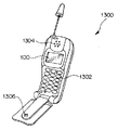
さらに、上記液晶装置を、携帯電話に適用した例について説明する。図14はこの携帯電話の構成を示す斜視図である。同図において、携帯電話1300は、複数の操作ボタン1302のほか、受話口1304、送話口1306と共に、液晶装置100を備えるものである。
【0103】
この液晶装置100にも、必要に応じてその前面にフロントライトが設けられる。また、この構成でも、液晶装置100が反射直視型として用いられることになるので、画素電極118に凹凸が形成される構成が望ましい。
【0104】
なお、電子機器としては、図13、図14を参照して説明した他にも、液晶テレビや、ビューファインダ型、モニタ直視型のビデオテープレコーダ、カーナビゲーション装置、ページャ、電子手帳、電卓、ワードプロセッサ、ワークステーション、テレビ電話、POS端末、タッチパネルを備えた機器等等が挙げられる。そして、これらの各種電子機器に対して、上記各実施形態や応用形態に係る液晶装置が適用可能なのは言うまでもない。
【0105】
また、上記実施の形態においては、1H期間内の反転駆動とフレーム反転駆動とを組み合わせた例について説明したが、1H期間内の反転駆動と1H反転、ソース反転又はドット反転駆動との組み合わせにも適用可能である。
【図面の簡単な説明】
【図1】本発明の一実施の形態に係る液晶装置を示すブロック図。
【図2】図1中の画素の具体的な構成を示す説明図。
【図3】図1中の極性反転回路302からの画像信号に基づいてソース線114に供給される画像信号の波形(ソース波形)を示す波形図。
【図4】実施の形態の動作を説明するためのタイミングチャート。
【図5】本実施の形態による縦クロストークの軽減効果を説明するための説明図。
【図6】本実施の形態による縦クロストークの軽減効果を説明するための波形図。
【図7】本実施の形態による縦クロストークの軽減効果を説明するための波形図。
【図8】本実施の形態の変形例を示す波形図。
【図9】本実施の形態の変形例を示す波形図。
【図10】本実施の形態に係る液晶装置の構造を説明するための平面図。
【図11】本実施の形態に係る液晶装置の構造を説明するための断面図。
【図12】本実施の形態に係る液晶装置をライトバルブとして用いたプロジェクタを示す平面図。
【図13】本発明に係る電子機器としてのパーソナルコンピュータの構成を示す斜視図。
【図14】本発明に係る電子機器としての携帯電話の構成を示す斜視図。
【図15】従来例の問題点を説明するための説明図。
【図16】図15に対応した液晶駆動電圧を説明するための波形図。
【図17】図15に対応した液晶駆動電圧を説明するための波形図。
【符号の説明】
101a…表示領域、301…駆動回路、302…極性反転回路、401…Yドライバ、500…Xドライバ。[0001]
TECHNICAL FIELD OF THE INVENTION
The present invention relates to a voltage modulation type liquid crystal device that reduces vertical crosstalk, a driving method thereof, and an electronic apparatus.
[0002]
[Prior art]
2. Description of the Related Art Electro-optical devices, for example, liquid crystal display devices using liquid crystal as an electro-optical material are widely used as display devices in place of cathode ray tubes (CRTs) for display units of various information processing apparatuses and liquid crystal televisions.
[0003]
Such a liquid crystal display device includes, for example, an element substrate provided with pixel electrodes arranged in a matrix, a switching element such as a TFT (Thin Film Transistor) connected to the pixel electrodes, and a pixel electrode. And a liquid crystal, which is an electro-optical material, filled between the two substrates.
[0004]
The display modes of the liquid crystal display device having such a configuration include a normally white mode for displaying white when no voltage is applied and a normally black mode for displaying black.
[0005]
Next, an operation of displaying an image in gradation in a liquid crystal display device will be described.
[0006]
The switching element is turned on by a scanning signal (gate signal) supplied via a scanning line (gate line). An image signal of a voltage corresponding to the gradation is applied to the pixel electrode via the data line (source line) in a state where the scanning element is turned on by applying the scanning signal. Then, charges corresponding to the voltage of the image signal are accumulated in the pixel electrode and the counter electrode. After the charge accumulation, even if the scanning signal is removed and the switching element is turned off, the charge accumulation state in each electrode is maintained by the capacitance of the liquid crystal layer, the storage capacitance, and the like.
[0007]
As described above, when each switching element is driven and the amount of charge to be stored is controlled according to the gradation, the alignment state of the liquid crystal changes for each pixel, the light transmittance changes, and the brightness changes for each pixel. be able to. Thus, gradation display can be performed.
[0008]
Considering the capacitance of the liquid crystal layer and the storage capacitor, it is only necessary to apply a charge to the liquid crystal layer of each pixel only during a part of the period. Therefore, when driving a plurality of pixels arranged in a matrix, a scanning signal is simultaneously applied to each pixel connected to the same scanning line by each scanning line, and an image signal is applied to each pixel via a data line. The scanning lines for supplying and supplying the image signals may be sequentially switched. That is, in the liquid crystal display device, time-division multiplex driving in which a scanning line and a data line are shared by a plurality of pixels can be performed.
[0009]
In a liquid crystal device, for example, the application of a DC component of an applied signal causes decomposition of the liquid crystal component, contamination by impurities in the liquid crystal cell, and a phenomenon such as burn-in of a displayed image. Therefore, in general, inversion driving is performed in which the polarity of the driving voltage of each pixel electrode is inverted for each frame of an image signal, for example. The surface inversion drive such as the frame inversion drive is a method in which the polarity of the drive voltage of all the pixel electrodes constituting the image display area is all the same, and the drive voltage is inverted at a constant period.
[0010]
As described above, in the liquid crystal device, the driving voltage is applied to the pixel only in a part of the period in consideration of the capacitance. However, even during the period in which the drive voltage is not applied, the voltage applied to the pixel changes due to the influence of the coupling capacitance and the leakage of the charge. Due to such a potential fluctuation, the deterioration of the image quality becomes conspicuous, particularly in the halftone area.
[0011]
FIG. 15 is an explanatory diagram for explaining such a problem, and FIGS. 16 and 17 are waveform diagrams for explaining a liquid crystal driving potential corresponding to FIG. Vs in FIGS. 16 and 17 indicates the potential applied to the source line, and VA (solid line) and VB (dashed line) in FIGS. 16 and 17 indicate the application of the pixel electrode at points A and B in the drawings, respectively. The potential is shown. FIG. 16 shows a vertical crosstalk phenomenon due to capacitive coupling, and FIG. 17 shows a vertical crosstalk phenomenon due to current leakage.
[0012]
Now, assume that a rectangular black is displayed at the center of the screen, and an image signal for displaying a halftone gray display is provided to the liquid crystal panel in other areas of the screen. FIG. 15 shows a display on the entire screen of the liquid crystal panel in this case. As shown in FIG. 15, in this case, an image portion darker than the original gray display is displayed above the black display portion, and an image portion brighter than the original gray display is displayed below the black display portion. Will be done.
[0013]
Vs in FIGS. 16 and 17 indicates a source potential waveform applied to the center in the left-right direction of such an image, for example, a source line corresponding to the position of a vertical line passing through points A and B in FIG. . The N frame in FIGS. 16 and 17 is a waveform when the liquid crystal is driven in the positive polarity, and the (N + 1) frame is a waveform when the liquid crystal is driven in the negative polarity. In the periods T1 and T2 corresponding to the display of the black portion in FIG. 15, the difference between the source potential and the potential of the counter electrode (counter potential) is large. And the difference is smaller.
[0014]
In VA and VB of FIG. 16, the waveforms obtained by changing the periods T1 and T2 to dashed lines indicate ideal applied potential waveforms of the pixel electrode where no vertical crosstalk occurs. At timing t1 corresponding to the screen vertical position at point A of the Nth frame, the TFT of the pixel at point A is turned on, and the pixel electrode at point A has an image signal (drive potential) of a level corresponding to gray display of halftone. Is applied. At the timing when the image signal is supplied to the pixel on the line next to the point A, the TFT of the pixel at the point A is off, and the driving potential of the pixel electrode at the point A is held by the liquid crystal capacitance and the additional capacitance. At the timing corresponding to the screen A vertical position at the point A in the (N + 1) th frame, a negative drive potential is applied to the pixel at the point A. This driving potential is also held until the next N + 2 frames. The same applies to the point B, and the driving potential applied to the pixel electrode of the pixel at the point B is held until the next frame by the liquid crystal capacitance and the additional capacitance.
[0015]
However, the pixel electrode is affected by the source line potential even when the TFT is off due to the coupling capacitance and the leakage of electric charge. That is, as shown by VA and VB in FIGS. 16 and 17, in the period T1, the driving potentials of the pixels at the points A and B become higher than the level based on the image signal, as indicated by the hatched portions, In the period T2, the driving potential of the pixels at the points A and B becomes lower than the level based on the image signal. As a result, the driving potential of the pixel at point A becomes VA, and the driving potential of the pixel at point B becomes VB. In the periods T1 and T2, the difference between the driving potential and the opposing potential is increased at point A and becomes darker than gray display, and the difference between the driving potential and the opposing potential is reduced at point B and becomes brighter than gray display. Would.
[0016]
In order to avoid such a problem, in the liquid crystal device, inversion driving that combines inversion driving processing for each frame and line inversion driving for changing the polarity of the driving potential for each line, for example, is adopted. .
[0017]
As an apparatus for performing such a line inversion drive, there is an apparatus disclosed in Japanese Patent Application Laid-Open No. H11-163873.
[0018]
[Patent Document 1]
JP 05-61440 A
[0019]
[Problems to be solved by the invention]
However, in line inversion driving or the like, an electric field (hereinafter referred to as a horizontal electric field) is generated between adjacent pixel electrodes on the same substrate in a column direction or a row direction to which voltages having different polarities are applied. This horizontal electric field affects the rotation of the liquid crystal molecules in the tilt direction. That is, when line inversion is performed, a potential difference is generated between adjacent pixels, and an electric field is generated between adjacent pixels. Due to the influence of the electric field, a liquid crystal device that controls the alignment state of the liquid crystal by an electric field generated between the pixel electrode and the counter electrode has a problem that the image quality is deteriorated.
[0020]
The present invention has been made in view of such a problem, and it is possible to avoid the effects of coupling capacitance, charge leakage, lateral electric field, and the like by combining surface inversion driving and 1/2 line inversion driving. Accordingly, it is an object to provide a liquid crystal device capable of improving image quality, a driving method thereof, and an electronic device.
[0021]
[Means for Solving the Problems]
In the liquid crystal device according to the present invention, a pixel is formed corresponding to each intersection of a plurality of source lines and a plurality of gate lines arranged in a lattice, and provided in the pixel by a gate signal supplied to the gate line. When the switching element is turned on, a source voltage supplied to the source line is supplied to a pixel electrode of each pixel via the switching element, and the gate signal is supplied to a liquid crystal display unit in which liquid crystal is driven. And a Y driver for sequentially supplying the source line to the gate line, and inverting the polarity of an image signal input during a period for driving one line of pixels in the gate line direction of the liquid crystal display unit, so that the source line is connected to the source line. X driver means for supplying a voltage.
[0022]
According to such a configuration, in the liquid crystal display unit, pixels are configured corresponding to respective intersections of the plurality of source lines and the plurality of gate lines arranged in a grid pattern, and the pixels are supplied from the Y driver to the gate lines. The switching element provided in the pixel is turned on by the gate signal, whereby the source voltage supplied to the source line is supplied to the pixel electrode of each pixel via the switching element, and the liquid crystal is driven. The source voltage supplied to the source line is obtained by inverting the polarity of the input image signal in a period for driving one line of pixels in the gate line direction of the liquid crystal display unit by the X driver means. Finally, the source voltage of the polarity applied in the latter half of the period for driving one line of pixels in the gate line direction of the liquid crystal display portion is written in the liquid crystal. Therefore, the liquid crystal of all the pixels of the liquid crystal display section is written with the same polarity during the same frame period, and no horizontal electric field is generated. Further, the polarity of the source voltage is inverted during a period for driving one line of pixels in the gate line direction of the liquid crystal display portion. Therefore, even when the pixel electrode is affected by the source voltage, the influence of the source voltage is not affected by the liquid crystal display. Are averaged during the period of driving one line of pixels in the direction of the gate line of the section, and the change in the effective voltage during the off period of the switching element is cancelled. Thereby, vertical crosstalk due to the influence of the source voltage is reduced.
[0023]
Further, the Y driver is configured to perform at least one of a period before and after a switching timing from one polarity to the other polarity or from the other polarity to the one polarity of the image signal inverted by the X driver means, A gate signal for supplying the source voltage to the pixel electrode is generated.
[0024]
According to such a configuration, the source voltage having the polarity applied in the second half of the period for driving one line of pixels in the gate line direction of the liquid crystal display portion or the source voltage having the polarity applied in the first half is applied to the liquid crystal. Written. Therefore, the liquid crystal of all the pixels of the liquid crystal display section is written with the same polarity during the same frame period, and no horizontal electric field is generated.
[0025]
Further, the X driver means switches the switching timing of the image signal from one polarity to the other polarity or from the other polarity to one polarity by 1 / th of a period for driving one line of pixels in the gate line direction of the liquid crystal display unit. 2 is set.
[0026]
According to such a configuration, the positive drive period and the negative drive period are equal, and the effect of the source voltage can be effectively suppressed.
[0027]
Further, the X driver means switches the switching timing of the image signal from one polarity to the other polarity or from the other polarity to one polarity by 1 / th of a period for driving one line of pixels in the gate line direction of the liquid crystal display unit. The timing is set to a timing other than 2.
[0028]
According to such a configuration, the positive drive period and the negative drive period can be appropriately set, and the setting according to the driving capability of the X driver means is possible.
[0029]
Further, the Y driver may be configured to operate in one of a period before and after a switching timing from one polarity to the other polarity or from the other polarity to the one polarity of the image signal inverted by the X driver means. Generating a gate signal for supplying the source voltage to the pixel electrode, wherein the X driver means drives the pixel of one line in the direction of the gate line of the liquid crystal display section and the source voltage to the pixel. The level of the source voltage is changed according to a ratio to a period during which a gate signal to be supplied to the electrode is generated.
[0030]
According to such a configuration, even when the positive drive period and the negative drive period are different, a source voltage of a level corresponding to the ratio between these periods is supplied to the pixel electrode, so that the influence of the source voltage is reduced. It can be suppressed effectively.
[0031]
Further, the X driver means inverts the polarity of the image signal input every period of driving the pixels of all lines of the liquid crystal display unit and supplies the inverted signal to the source line as the source voltage. .
[0032]
According to such a configuration, the source voltage supplied to the source line is inverted by the X driver means during the period in which the input image signal drives one line of pixels in the gate line direction of the liquid crystal display unit. At the same time, the polarity is inverted every period during which the pixels of all lines of the liquid crystal display section are driven. Finally, the source voltage of the polarity applied in the latter half of the period for driving one line of pixels in the gate line direction of the liquid crystal display portion is written in the liquid crystal. Therefore, although the polarity of the liquid crystal of all pixels of the liquid crystal display unit is inverted between the preceding and succeeding frames, writing is performed with the same polarity during the same frame period, and no horizontal electric field is generated.
[0033]
Further, in the driving method of the liquid crystal device according to the present invention, a pixel is formed corresponding to each intersection of a plurality of source lines and a plurality of gate lines arranged in a grid, and a gate signal supplied to the gate line is provided. When a switching element provided in the pixel is turned on, a source voltage supplied to the source line is supplied to a pixel electrode of each pixel via the switching element, and a liquid crystal display unit is driven. A process of sequentially supplying the gate signal to the gate line, and inverting the polarity of an input image signal during a period for driving one line of pixels in the direction of the gate line of the liquid crystal display unit. Supplying the source voltage to the line as the source voltage.
[0034]
According to such a configuration, the switching element provided in the pixel is turned on by the gate signal supplied to the gate line. Accordingly, the source voltage supplied to the source line is applied to the pixel electrode of each pixel via the switching element, and the liquid crystal is driven. The polarity of the input image signal is inverted during a period for driving one line of pixels in the gate line direction of the liquid crystal display unit, and the polarity is inverted for each period for driving pixels on all lines of the liquid crystal display unit. Supplied to the wire. Thus, the liquid crystal of all the pixels of the liquid crystal display section is written with the same polarity during the same frame period, and no horizontal electric field is generated. Further, the polarity of the source voltage is inverted during a period for driving one line of pixels in the gate line direction of the liquid crystal display portion. Therefore, even when the pixel electrode is affected by the source voltage, the influence of the source voltage is not affected by the liquid crystal display. Are averaged during the period of driving one line of pixels in the direction of the gate line of the section, and the change in the effective voltage during the off period of the switching element is cancelled. Thereby, vertical crosstalk due to the influence of the source voltage is reduced.
[0035]
In addition, the process of supplying a source voltage to the source line includes a process of inverting the polarity of the input image signal every period during which pixels on all lines of the liquid crystal display unit are driven.
[0036]
According to such a configuration, the polarity of the input image signal is inverted during the period of driving one line of pixels in the gate line direction of the liquid crystal display unit, and the pixels of all lines of the liquid crystal display unit are driven. The polarity is inverted every period and supplied to the source line. As a result, the polarity of the liquid crystal of all the pixels of the liquid crystal display unit is inverted between the previous and next frames, but writing is performed with the same polarity during the same frame period, and no horizontal electric field is generated.
[0037]
According to another aspect of the invention, an electronic apparatus includes the above-described liquid crystal device.
[0038]
According to such a configuration, a high-quality image in which the adverse effects of the horizontal electric field and the vertical crosstalk are avoided can be obtained.
[0039]
BEST MODE FOR CARRYING OUT THE INVENTION
Hereinafter, embodiments of the present invention will be described in detail with reference to the drawings. FIG. 1 is a block diagram showing a liquid crystal device according to one embodiment of the present invention.
[0040]
In this embodiment mode, the liquid crystal is driven by inverting the polarity every (1/2) H (horizontal period) and every frame period in order to avoid the adverse effects due to the coupling capacitance and charge leakage and the adverse effects due to the lateral electric field. It is like that.
[0041]
The liquid crystal device according to the present embodiment includes a display area 101a using liquid crystal which is an electro-optical material, a
[0042]
In a liquid crystal device, a transparent substrate such as a glass substrate is used as an element substrate, and a peripheral driving circuit and the like are formed on the element substrate along with transistors for driving pixels. A plurality of gate lines (scanning lines) 112 are formed in the display area 101 a on the element base, extending in the X (row) direction in FIG. 1, and a plurality of source lines (data lines) 114 Are formed extending along the Y (column) direction. The
[0043]
FIG. 2 is an explanatory diagram showing a specific configuration of the pixel in FIG.
[0044]
Each
[0045]
A counter electrode voltage VLCCOM is applied to the
[0046]
Each
[0047]
The
[0048]
That is, the timing generator generates a transfer clock CLX and a data enable signal ENBX, which are signals for driving the display, and outputs them to the
[0049]
The polarity inversion signal FR generated by the timing generator is a signal that is inverted every frame. The polarity inversion signal FHL is a signal that is inverted every (1 /) H. The scan start pulse DY is a pulse signal output at the start point of each frame. When the scan start pulse DY is input to the
[0050]
The transfer clock CLY is a signal that defines the scanning speed on the scanning side (Y side), and gate pulses (G1 to Gm) are sent for each gate line in synchronization with the transfer clock. The data enable signal ENBX determines the timing at which image signals held in a sampling and holding circuit (not shown) in the
[0051]
In FIG. 1, a
[0052]
The
[0053]
In this embodiment, the
FIG. 3 is a waveform diagram showing a waveform (source waveform) of an image signal supplied to the
[0054]
As shown in FIGS. 3A and 3B, in the first frame, the image signal has a positive polarity in the first half of each horizontal period, and has a negative polarity in the second half of each horizontal period. I have. In the second frame, the image signal has a negative polarity in the first half of each horizontal period, and has a positive polarity in the second half of each horizontal period. That is, the image signal is inverted every (1/2) H period, and is also inverted every frame period.
[0055]
Next, the operation of the embodiment configured as described above will be described with reference to FIGS. 4 is a timing chart showing a gate signal (gate pulse) output from the
[0056]
Now, it is assumed that an image signal having a constant level in the Nth frame and the (N + 1) th frame, for example, an image signal for displaying the same color (solid display) on the entire screen is supplied to the
[0057]
On the other hand, the
[0058]
Assuming that the
[0059]
In the present embodiment, the source voltage is inverted every (1 /) H period. However, in the Nth frame, the source voltage is positive in the latter half of each horizontal period, and the liquid crystal is finally driven with positive polarity. Conversely, in the (N + 1) th frame, the source voltage is negative in the latter half of each horizontal period, and finally the liquid crystal is driven with negative polarity. That is, in the examples of FIGS. 4A and 4B, the liquid crystal is driven with a positive polarity in the Nth frame, and is driven with a negative polarity in the N + 1th frame. Therefore, the liquid crystal is driven by the same drive voltage as that in the frame inversion drive.
[0060]
That is, in the same frame, all pixels have the same polarity, and no horizontal electric field is generated between adjacent upper and lower pixels.
In the example of FIG. 4B, the driving method of the
[0061]
FIG. 4C shows an example of this case. In the example of FIG. 4C, the gate pulse in the first half of each horizontal period is a low level (hereinafter, referred to as “L”) and the second half is “H”. That is, in this case, the
[0062]
Also, the gate pulse shown in FIG. 4D can be employed. In the example of FIG. 4D, the gate pulse in the first half of each horizontal period is “H” and the latter half is “L”. That is, in this case, the
[0063]
Next, the effect of reducing vertical crosstalk according to the present embodiment will be described with reference to FIGS. FIG. 5 shows an image in which the center of the screen is rectangular black display and the other screen areas are halftone gray display. FIG. 6 is a waveform chart for explaining an ideal liquid crystal drive voltage for displaying the image of FIG. 5, and FIG. 7 is a waveform chart for explaining the liquid crystal drive voltage in the present embodiment. Although the number of waves of the source waveform is the same as the number of gate lines in FIGS. 6 and 7, the number of pulses in one frame period is less than the actual number for simplification of the drawing.
[0064]
6 (b) and 7 (b) show the voltages applied to the source line, and VA (solid line) and VB (dotted line) in FIGS. 6 (a) and 7 (a) respectively indicate The voltage applied to the pixel electrode at points A and B is shown. FIG. 7 shows a drive voltage waveform when capacitive coupling occurs.
[0065]
As shown in FIGS. 6B and 7B, the source voltage waveform applied to the source line corresponding to the center in the horizontal direction of the image, for example, the vertical line passing through points A and B in FIG. Are inverted every (1 /) H period by the
[0066]
FIG. 6 shows an ideal applied voltage waveform of the pixel electrode where no vertical crosstalk occurs in the pixel at the point A. At timing t1 corresponding to the screen vertical position at point A of the Nth frame, the TFT of the pixel at point A is turned on, and the pixel electrode at point A has an image signal (drive voltage) of a level corresponding to gray display of halftone. Is applied. At the timing when the image signal is supplied to the pixel on the line next to the point A, the TFT of the pixel at the point A is off, and the driving voltage of the pixel electrode at the point A is held by the liquid crystal capacitance and the additional capacitance. At the timing corresponding to the screen vertical position at point A in the (N + 1) th frame, a negative drive voltage is applied to the pixel at point A, and this drive voltage is also held until the next N + 2 frame. The same applies to the point B, and the driving voltage applied to the pixel electrode of the pixel at the point B is held until the next frame. In this manner, the grayscale display of the halftone is performed at the points A and B, similarly to the point C in FIG.
[0067]
However, as shown in FIGS. 16 and 17 described above, actually, the applied voltage of the pixel electrode is affected by the source line voltage due to the coupling capacitance and the leakage of the electric charge, and the pixel at the point A in the black display period. In this case, the difference between the driving potential and the opposing potential becomes large, and the difference between the driving potential and the opposing potential becomes small in the pixel at point B.
[0068]
On the other hand, in the present embodiment, as described above, a source voltage that is inverted every (1 /) H period is supplied to the pixel electrode of each pixel. FIG. 7 shows a drive voltage waveform when each pixel is affected by capacitive coupling in this case.
[0069]
As shown in FIG. 7A, the driving voltage applied to each pixel is inverted in the (1/2) H period and in one frame period. For example, by applying the gate pulse shown in FIG. 4B, in the Nth frame, a drive voltage that changes from positive to negative and finally becomes negative is applied to the pixel electrode of each pixel. In the (N + 1) th frame, a drive voltage is changed from negative polarity to positive polarity and finally to positive polarity. By applying the gate pulse shown in FIG. 4C, a negative drive voltage is applied to the pixel electrode of each pixel in the Nth frame, and a positive drive voltage is applied in the (N + 1) th frame. Is done. Further, by applying the gate pulse shown in FIG. 4D, a positive drive voltage is applied to the pixel electrode of each pixel in the Nth frame, and a negative drive voltage is applied in the (N + 1) th frame. Is done.
[0070]
When capacitive coupling occurs, each pixel electrode is affected by the source line voltage. FIG. 7A shows this state, and each pixel electrode fluctuates at a level corresponding to the level of the source voltage due to the influence of the change in the source voltage. However, since the source voltage is inverted every (1 /) H period, this variation changes according to the source voltage in the inversion cycle of the source voltage. That is, in both the halftone display period and the black display period, the applied voltage to the pixel electrode is driven to be inverted every (1 /) H period which is a relatively short cycle.
[0071]
In the halftone display period, the voltage applied to the source line is smaller than the voltage required for black display, and the fluctuation range of the potential on the positive electrode side and the negative electrode side is small. That is, the effective value of the drive voltage during the halftone display period is substantially equal to the effective value of the halftone when an ideal voltage is applied to the pixel.
[0072]
In the analog drive (voltage modulation drive), the liquid crystal is driven at a drive voltage or less that saturates the transmittance of the liquid crystal, and the transmittance of the liquid crystal is substantially proportional to the effective value (integral value) of the drive voltage applied to the pixel electrode. Thus, a screen having a brightness proportional to the effective value of the drive voltage is obtained. Therefore, in the halftone display period, from the viewpoint of the effective value, the luminance becomes almost equal to the halftone luminance when an ideal voltage is applied to the pixel.
[0073]
On the other hand, in the black display period in which a high voltage required for black display is applied to the source line, when the voltage applied to the source line is always of the same polarity within the 1H period as in the conventional example, the black display is performed. A necessary high voltage is applied to the source line, and the potential applied to the pixel always greatly fluctuates to one side in one frame due to capacitive coupling between the source line and the pixel electrode. Due to the fluctuation of the pixel potential, as described above, the effective voltage of the liquid crystal of the pixel A increases and the effective voltage of the liquid crystal of the pixel B decreases, and crosstalk occurs due to the change in luminance.
[0074]
However, in the present embodiment, the inversion driving method is employed for each (1/2) H period, and even when a high voltage necessary for black display is applied to the source line, the bipolar driving is performed within the 1H period. A voltage will be applied to the pixel electrode. In this case, since the pixel applied voltage fluctuates on both the positive electrode side and the negative electrode side, the effective value of the liquid crystal applied voltage is substantially equal to the effective value of the applied voltage when not affected by the source line. That is, a driving voltage having an effective value substantially the same as the driving voltage for the pixel C is applied to the liquid crystal, and the original gray display portion is displayed with substantially uniform brightness in any screen area.
[0075]
Although the effect on the capacitive coupling has been described with reference to FIG. 7, it is clear that the effect of the current leakage can be similarly reduced by the (1/2) H period inversion drive.
[0076]
As described above, in the present embodiment, the liquid crystal is subjected to the frame inversion driving and the ()) H inversion driving, so that the influence of the horizontal electric field can be avoided and the vertical crosstalk can be improved.
[0077]
By the way, in the above-described embodiment, an example in which the liquid crystal is inverted and driven every (1/2) H period and every one frame period has been described. In the present invention, it is only necessary to invert the liquid crystal in the positive polarity and the negative polarity in the 1H period, and it is not always necessary to invert the liquid crystal every (() H period. For example, depending on the driving capability of the X driver, the time of the polarity finally applied to the pixel electrode can be set shorter than the (1/2) H period. Conversely, it can be set longer than the (1/2) H period.
[0078]
FIG. 8 is a waveform diagram showing an example in this case. FIG. 8 is a waveform diagram showing the relationship between the gate pulse and the source potential. The source potential is shown on the upper side and the gate pulse is shown on the lower side corresponding to FIG. FIG. 8A shows (() H inversion driving similar to the above embodiment, FIG. 8B shows (3/4) H inversion driving, and FIG. 4) H inversion drive is shown. In FIG. 8, for simplification of the drawing, the number of pulses in one frame period is smaller than the actual number.
[0079]
FIG. 8A shows the same gate pulse and source voltage as in FIGS. 4A and 4B. FIG. 8B shows an example in which the polarity is inverted at the timing of the first (period of the 1H period in the
[0080]
On the other hand, FIG. 8C shows an example in which the polarity is inverted in the
[0081]
As described above, the polarity may be inverted in the 1H period, and the polarity may be inverted not only in the (1 /) H period but also in an arbitrary division ratio in the 1H period.
[0082]
By the way, when the voltage supplied to the source line is asymmetric as in the examples of FIGS. 8B and 8C, the voltage fluctuation in FIG. 7 is also asymmetric, and the effective voltage applied to the liquid crystal is ideal. It changes from the value. Therefore, it is conceivable to change the voltage applied to the source line in order to make the effective voltage applied to the liquid crystal closer to an ideal value. FIG. 9 shows an example in this case.
[0083]
FIG. 9 is a waveform diagram showing the relationship between the gate pulse and the source potential. The source potential is shown on the upper side and the gate pulse is shown on the lower side corresponding to FIG. FIG. 9A shows the same (1 /) H inversion drive as that of the above embodiment, and FIG. 9B shows the (1 /) H inversion corresponding to FIGS. 4C and 8C. This shows inversion driving. In FIG. 9, the number of pulses in one frame period is smaller than the actual number in order to simplify the drawing.
[0084]
FIG. 9A shows the same gate pulse and source voltage as in FIGS. 4A and 4C. FIG. 9B shows a gate pulse corresponding to FIGS. 4C and 8C. That is, in the example of FIG. 9, the (() H inversion drive is employed, and at the same time, the
[0085]
Depending on the response of the liquid crystal, when the writing time of the pixel electrode is short, the liquid crystal may not increase to a desired writing voltage corresponding to the image signal. Even in this case, the liquid crystal is driven at a desired writing voltage corresponding to the image signal by increasing the source voltage according to the level of the image signal and the writing time to the pixel electrode as in the example of FIG. It is possible to do.
[0086]
Next, the structure of the liquid crystal device according to the above-described embodiment or application will be described with reference to FIGS. Here, FIG. 10 is a plan view showing the configuration of the
[0087]
As shown in these drawings, in the
[0088]
The opposing
[0089]
In the
[0090]
That is, the light-shielding
[0091]
In the
[0092]
On the other hand, the opposing
[0093]
In addition, depending on the application of the
[0094]
Next, some examples in which the above-described liquid crystal device is used in specific electronic devices will be described.
[0095]
First, a projector using the liquid crystal device according to the embodiment as a light valve will be described. FIG. 12 is a plan view showing the configuration of this projector. As shown in this figure, inside the
[0096]
The s-polarized light beam emitted from the polarized
[0097]
On the other hand, among the light beams transmitted through the blue light reflecting layer of the
[0098]
In this way, the red, green, and blue lights modulated by the
[0099]
In the present embodiment, a reflection type liquid crystal device is used, but a projector using a transmission type liquid crystal device may be used.
[0100]
Next, an example in which the liquid crystal device is applied to a mobile personal computer will be described. FIG. 13 is a perspective view showing the configuration of this personal computer. In the figure, a
[0101]
In this configuration, since the
[0102]
Further, an example in which the liquid crystal device is applied to a mobile phone will be described. FIG. 14 is a perspective view showing the configuration of the mobile phone. In the figure, a
[0103]
The
[0104]
In addition to the electronic devices described with reference to FIGS. 13 and 14, a liquid crystal television, a viewfinder type, a monitor direct-view type video tape recorder, a car navigation device, a pager, an electronic notebook, a calculator, a word processor , A workstation, a videophone, a POS terminal, a device equipped with a touch panel, and the like. Needless to say, the liquid crystal device according to each of the above embodiments and application forms can be applied to these various electronic devices.
[0105]
Further, in the above-described embodiment, an example in which inversion driving and frame inversion driving in the 1H period are combined has been described. However, a combination of inversion driving and 1H inversion, source inversion, or dot inversion driving in the 1H period is also applicable. Applicable.
[Brief description of the drawings]
FIG. 1 is a block diagram showing a liquid crystal device according to one embodiment of the present invention.
FIG. 2 is an explanatory diagram showing a specific configuration of a pixel in FIG.
3 is a waveform diagram showing a waveform (source waveform) of an image signal supplied to a
FIG. 4 is a timing chart illustrating operation of the embodiment.
FIG. 5 is an explanatory diagram for explaining an effect of reducing vertical crosstalk according to the embodiment;
FIG. 6 is a waveform chart for explaining the effect of reducing vertical crosstalk according to the present embodiment.
FIG. 7 is a waveform chart for explaining the effect of reducing vertical crosstalk according to the present embodiment.
FIG. 8 is a waveform chart showing a modification of the present embodiment.
FIG. 9 is a waveform chart showing a modification of the present embodiment.
FIG. 10 is a plan view illustrating a structure of a liquid crystal device according to this embodiment.
FIG. 11 is a cross-sectional view illustrating a structure of a liquid crystal device according to this embodiment.
FIG. 12 is a plan view showing a projector using the liquid crystal device according to the present embodiment as a light valve.
FIG. 13 is a perspective view showing a configuration of a personal computer as an electronic apparatus according to the invention.
FIG. 14 is a perspective view showing a configuration of a mobile phone as an electronic device according to the invention.
FIG. 15 is an explanatory diagram for explaining a problem of the conventional example.
FIG. 16 is a waveform chart for explaining a liquid crystal drive voltage corresponding to FIG.
FIG. 17 is a waveform chart for explaining a liquid crystal drive voltage corresponding to FIG.
[Explanation of symbols]
101a: display area, 301: drive circuit, 302: polarity inversion circuit, 401: Y driver, 500: X driver.
Claims (9)
前記液晶表示部の前記ゲート線方向の1ラインの画素を駆動する期間内において入力された画像信号の極性を反転させて、前記ソース線に前記ソース電圧として供給するXドライバ手段とを具備したことを特徴とする液晶装置。A pixel is formed corresponding to each intersection of the plurality of source lines and the plurality of gate lines arranged in a lattice, and a switching element provided in the pixel is turned on by a gate signal supplied to the gate line. Accordingly, the source signal supplied to the source line is supplied to the pixel electrode of each pixel via the switching element, and the gate signal is sequentially supplied to the gate line to a liquid crystal display unit in which liquid crystal is driven. A Y driver,
X driver means for inverting the polarity of an input image signal during a period for driving one line of pixels in the gate line direction of the liquid crystal display unit and supplying the source signal to the source line as the source voltage. A liquid crystal device characterized by the above-mentioned.
前記Xドライバ手段は、前記液晶表示部の前記ゲート線方向の1ラインの画素を駆動する期間と前記ソース電圧を前記画素電極に供給するためのゲート信号が発生している期間との割合に応じて、前記ソース電圧のレベルを変化させることを特徴とする請求項1に記載の液晶装置。The Y driver is configured to control the image signal, which is inverted by the X driver means, during one of a period before and after a switching timing from one polarity to the other polarity or from the other polarity to the one polarity. Generating a gate signal for supplying a source voltage to the pixel electrode;
The X driver means determines a ratio between a period during which one line of pixels in the gate line direction of the liquid crystal display unit is driven and a period during which a gate signal for supplying the source voltage to the pixel electrode is generated. 2. The liquid crystal device according to claim 1, wherein the level of the source voltage is changed.
前記液晶表示部の前記ゲート線方向の1ラインの画素を駆動する期間内において入力された画像信号の極性を反転させて、前記ソース線に前記ソース電圧として供給する処理とを具備したことを特徴とする液晶装置の駆動方法。A pixel is formed corresponding to each intersection of the plurality of source lines and the plurality of gate lines arranged in a lattice, and a switching element provided in the pixel is turned on by a gate signal supplied to the gate line. Accordingly, the source signal supplied to the source line is supplied to the pixel electrode of each pixel via the switching element, and the gate signal is sequentially supplied to the gate line to a liquid crystal display unit in which liquid crystal is driven. Processing,
A process of inverting the polarity of an input image signal during a period for driving one line of pixels in the gate line direction of the liquid crystal display unit and supplying the inverted signal to the source line as the source voltage. Driving method for a liquid crystal device.
Priority Applications (1)
| Application Number | Priority Date | Filing Date | Title |
|---|---|---|---|
| JP2003024080A JP2004233807A (en) | 2003-01-31 | 2003-01-31 | Liquid crystal device and its driving method, and electronic equipment |
Applications Claiming Priority (1)
| Application Number | Priority Date | Filing Date | Title |
|---|---|---|---|
| JP2003024080A JP2004233807A (en) | 2003-01-31 | 2003-01-31 | Liquid crystal device and its driving method, and electronic equipment |
Publications (1)
| Publication Number | Publication Date |
|---|---|
| JP2004233807A true JP2004233807A (en) | 2004-08-19 |
Family
ID=32952716
Family Applications (1)
| Application Number | Title | Priority Date | Filing Date |
|---|---|---|---|
| JP2003024080A Withdrawn JP2004233807A (en) | 2003-01-31 | 2003-01-31 | Liquid crystal device and its driving method, and electronic equipment |
Country Status (1)
| Country | Link |
|---|---|
| JP (1) | JP2004233807A (en) |
Cited By (3)
| Publication number | Priority date | Publication date | Assignee | Title |
|---|---|---|---|---|
| JP2009271267A (en) * | 2008-05-07 | 2009-11-19 | Casio Comput Co Ltd | Driver, display device, and driving method of the same |
| US8169555B2 (en) | 2006-09-19 | 2012-05-01 | Sony Corporation | Liquid crystal display device |
| CN107564483A (en) * | 2017-09-12 | 2018-01-09 | 惠科股份有限公司 | A kind of drive device of display panel, driving method and display device |
-
2003
- 2003-01-31 JP JP2003024080A patent/JP2004233807A/en not_active Withdrawn
Cited By (3)
| Publication number | Priority date | Publication date | Assignee | Title |
|---|---|---|---|---|
| US8169555B2 (en) | 2006-09-19 | 2012-05-01 | Sony Corporation | Liquid crystal display device |
| JP2009271267A (en) * | 2008-05-07 | 2009-11-19 | Casio Comput Co Ltd | Driver, display device, and driving method of the same |
| CN107564483A (en) * | 2017-09-12 | 2018-01-09 | 惠科股份有限公司 | A kind of drive device of display panel, driving method and display device |
Similar Documents
| Publication | Publication Date | Title |
|---|---|---|
| KR100632750B1 (en) | Driving circuit and driving method for electro-optical apparatus | |
| US7474302B2 (en) | Electro-optical device, driving method of electro-optical device, driving circuit of electro-optical device and electronic apparatus | |
| JP4114655B2 (en) | Brightness unevenness correction method, brightness unevenness correction circuit, electro-optical device, and electronic apparatus | |
| JP2003177723A (en) | Method for driving electro-optical device, driving circuit therefor, electro-optical device, and electronic equipment | |
| US6873319B2 (en) | Method for driving electrooptical device, driving circuit, and electrooptical device, and electronic apparatus | |
| US7358940B2 (en) | Electro-optical device, circuit for driving electro-optical device, method of driving electro-optical device, and electronic apparatus | |
| JP3659103B2 (en) | Electro-optical device, driving circuit and driving method of electro-optical device, and electronic apparatus | |
| JP2001075534A (en) | Liquid crystal display device | |
| JP3661523B2 (en) | Electro-optical device driving method, driving circuit, electro-optical device, and electronic apparatus | |
| JP3873544B2 (en) | Electro-optical device and projection display device | |
| JP2004233808A (en) | Liquid crystal device, its driving method, and electronic equipment | |
| JP2008076804A (en) | Electro-optical device and electronic apparatus with same | |
| JP4179289B2 (en) | Electro-optical device, driving method thereof, and electronic apparatus | |
| JP2004233807A (en) | Liquid crystal device and its driving method, and electronic equipment | |
| JP3800962B2 (en) | Electro-optical device, electronic apparatus, and projection display device | |
| JP4258501B2 (en) | Electro-optical device, electronic apparatus, and driving method of electro-optical device | |
| JP2005301170A (en) | Driving circuit for electro-optical device and driving method for electro-optical device, and electro-optical device and electronic equipment equipped therewith | |
| JP4386608B2 (en) | Electro-optical device, driving method thereof, and electronic apparatus | |
| JP3775137B2 (en) | Electro-optical device driving method, driving circuit, electro-optical device, and electronic apparatus | |
| JP4590879B2 (en) | Liquid crystal device, driving circuit of liquid crystal device, driving method thereof, and electronic apparatus | |
| JP3888076B2 (en) | Electro-optical device driving method, electro-optical device driving device, electro-optical device, and electronic apparatus | |
| JP4617680B2 (en) | Liquid crystal device, driving circuit of liquid crystal device, driving method thereof, and electronic apparatus | |
| JP2010026085A (en) | Driving device and method for electrooptical device, electrooptical device, and electronic apparatus | |
| JP2003186448A (en) | Driving method and driving circuit of electrooptic device, the electrooptic device, and electronic equipment | |
| JP2004233968A (en) | Liquid crystal device and its driving method, and electronic equipment |
Legal Events
| Date | Code | Title | Description |
|---|---|---|---|
| A300 | Withdrawal of application because of no request for examination |
Free format text: JAPANESE INTERMEDIATE CODE: A300 Effective date: 20060404 |