JP2004228551A - Method to produce substrate for use in transference and wiring plate - Google Patents
Method to produce substrate for use in transference and wiring plate Download PDFInfo
- Publication number
- JP2004228551A JP2004228551A JP2003149809A JP2003149809A JP2004228551A JP 2004228551 A JP2004228551 A JP 2004228551A JP 2003149809 A JP2003149809 A JP 2003149809A JP 2003149809 A JP2003149809 A JP 2003149809A JP 2004228551 A JP2004228551 A JP 2004228551A
- Authority
- JP
- Japan
- Prior art keywords
- metal film
- resin layer
- metal
- transfer substrate
- transfer
- Prior art date
- Legal status (The legal status is an assumption and is not a legal conclusion. Google has not performed a legal analysis and makes no representation as to the accuracy of the status listed.)
- Granted
Links
- 239000000758 substrate Substances 0.000 title claims abstract description 157
- 238000000034 method Methods 0.000 title claims abstract description 27
- 229910052751 metal Inorganic materials 0.000 claims abstract description 245
- 239000002184 metal Substances 0.000 claims abstract description 245
- 238000012546 transfer Methods 0.000 claims abstract description 182
- 229920005989 resin Polymers 0.000 claims abstract description 131
- 239000011347 resin Substances 0.000 claims abstract description 131
- 239000007769 metal material Substances 0.000 claims abstract description 38
- XEEYBQQBJWHFJM-UHFFFAOYSA-N Iron Chemical compound [Fe] XEEYBQQBJWHFJM-UHFFFAOYSA-N 0.000 claims description 162
- 229910052742 iron Inorganic materials 0.000 claims description 86
- 238000007747 plating Methods 0.000 claims description 75
- 239000000463 material Substances 0.000 claims description 72
- PXHVJJICTQNCMI-UHFFFAOYSA-N Nickel Chemical compound [Ni] PXHVJJICTQNCMI-UHFFFAOYSA-N 0.000 claims description 48
- 238000005530 etching Methods 0.000 claims description 47
- RYGMFSIKBFXOCR-UHFFFAOYSA-N Copper Chemical compound [Cu] RYGMFSIKBFXOCR-UHFFFAOYSA-N 0.000 claims description 31
- 239000010949 copper Substances 0.000 claims description 30
- 229910052802 copper Inorganic materials 0.000 claims description 29
- 229910052759 nickel Inorganic materials 0.000 claims description 26
- 229910021578 Iron(III) chloride Inorganic materials 0.000 claims description 19
- RBTARNINKXHZNM-UHFFFAOYSA-K iron trichloride Chemical compound Cl[Fe](Cl)Cl RBTARNINKXHZNM-UHFFFAOYSA-K 0.000 claims description 19
- 238000004519 manufacturing process Methods 0.000 claims description 17
- 229910021645 metal ion Inorganic materials 0.000 claims description 16
- 238000004381 surface treatment Methods 0.000 claims description 14
- 230000003746 surface roughness Effects 0.000 claims description 12
- 229910052804 chromium Inorganic materials 0.000 claims description 9
- 239000011651 chromium Substances 0.000 claims description 9
- -1 iron ions Chemical class 0.000 claims description 8
- PCHJSUWPFVWCPO-UHFFFAOYSA-N gold Chemical compound [Au] PCHJSUWPFVWCPO-UHFFFAOYSA-N 0.000 claims description 7
- 239000010931 gold Substances 0.000 claims description 7
- 229910052737 gold Inorganic materials 0.000 claims description 7
- 150000002500 ions Chemical class 0.000 claims description 6
- NMCUIPGRVMDVDB-UHFFFAOYSA-L iron dichloride Chemical compound Cl[Fe]Cl NMCUIPGRVMDVDB-UHFFFAOYSA-L 0.000 claims description 6
- 229960002089 ferrous chloride Drugs 0.000 claims description 5
- VYZAMTAEIAYCRO-UHFFFAOYSA-N Chromium Chemical compound [Cr] VYZAMTAEIAYCRO-UHFFFAOYSA-N 0.000 claims description 4
- 239000002023 wood Substances 0.000 claims 1
- 239000004020 conductor Substances 0.000 abstract description 35
- 238000010030 laminating Methods 0.000 abstract description 4
- 238000001721 transfer moulding Methods 0.000 abstract description 2
- 239000010410 layer Substances 0.000 description 124
- 239000000243 solution Substances 0.000 description 45
- 238000012545 processing Methods 0.000 description 23
- 229910001220 stainless steel Inorganic materials 0.000 description 22
- 239000010935 stainless steel Substances 0.000 description 22
- 238000000465 moulding Methods 0.000 description 19
- JPVYNHNXODAKFH-UHFFFAOYSA-N Cu2+ Chemical compound [Cu+2] JPVYNHNXODAKFH-UHFFFAOYSA-N 0.000 description 15
- 229910001431 copper ion Inorganic materials 0.000 description 15
- 238000007788 roughening Methods 0.000 description 14
- 230000005484 gravity Effects 0.000 description 11
- 230000033116 oxidation-reduction process Effects 0.000 description 11
- 229910000679 solder Inorganic materials 0.000 description 11
- 238000006243 chemical reaction Methods 0.000 description 9
- 230000000052 comparative effect Effects 0.000 description 8
- 238000007639 printing Methods 0.000 description 7
- 238000011156 evaluation Methods 0.000 description 6
- 239000011342 resin composition Substances 0.000 description 6
- 230000015572 biosynthetic process Effects 0.000 description 5
- FBAFATDZDUQKNH-UHFFFAOYSA-M iron chloride Chemical compound [Cl-].[Fe] FBAFATDZDUQKNH-UHFFFAOYSA-M 0.000 description 5
- 238000005498 polishing Methods 0.000 description 4
- 239000002344 surface layer Substances 0.000 description 4
- 229920001187 thermosetting polymer Polymers 0.000 description 4
- 239000003990 capacitor Substances 0.000 description 3
- 238000005553 drilling Methods 0.000 description 3
- 230000000694 effects Effects 0.000 description 3
- 239000003822 epoxy resin Substances 0.000 description 3
- 238000010438 heat treatment Methods 0.000 description 3
- 230000007774 longterm Effects 0.000 description 3
- 238000005259 measurement Methods 0.000 description 3
- 239000000203 mixture Substances 0.000 description 3
- 229910001453 nickel ion Inorganic materials 0.000 description 3
- 229920000647 polyepoxide Polymers 0.000 description 3
- 239000000126 substance Substances 0.000 description 3
- VEXZGXHMUGYJMC-UHFFFAOYSA-N Hydrochloric acid Chemical compound Cl VEXZGXHMUGYJMC-UHFFFAOYSA-N 0.000 description 2
- VEQPNABPJHWNSG-UHFFFAOYSA-N Nickel(2+) Chemical compound [Ni+2] VEQPNABPJHWNSG-UHFFFAOYSA-N 0.000 description 2
- 244000137852 Petrea volubilis Species 0.000 description 2
- 230000002411 adverse Effects 0.000 description 2
- 239000011889 copper foil Substances 0.000 description 2
- 229910000365 copper sulfate Inorganic materials 0.000 description 2
- ORTQZVOHEJQUHG-UHFFFAOYSA-L copper(II) chloride Chemical compound Cl[Cu]Cl ORTQZVOHEJQUHG-UHFFFAOYSA-L 0.000 description 2
- ARUVKPQLZAKDPS-UHFFFAOYSA-L copper(II) sulfate Chemical compound [Cu+2].[O-][S+2]([O-])([O-])[O-] ARUVKPQLZAKDPS-UHFFFAOYSA-L 0.000 description 2
- YPHMISFOHDHNIV-FSZOTQKASA-N cycloheximide Chemical compound C1[C@@H](C)C[C@H](C)C(=O)[C@@H]1[C@H](O)CC1CC(=O)NC(=O)C1 YPHMISFOHDHNIV-FSZOTQKASA-N 0.000 description 2
- 230000007613 environmental effect Effects 0.000 description 2
- 239000000945 filler Substances 0.000 description 2
- 239000011888 foil Substances 0.000 description 2
- 238000003475 lamination Methods 0.000 description 2
- 239000004065 semiconductor Substances 0.000 description 2
- 238000012360 testing method Methods 0.000 description 2
- 235000001674 Agaricus brunnescens Nutrition 0.000 description 1
- 229920002799 BoPET Polymers 0.000 description 1
- VEXZGXHMUGYJMC-UHFFFAOYSA-M Chloride anion Chemical compound [Cl-] VEXZGXHMUGYJMC-UHFFFAOYSA-M 0.000 description 1
- 229910021592 Copper(II) chloride Inorganic materials 0.000 description 1
- 229910021577 Iron(II) chloride Inorganic materials 0.000 description 1
- XUIMIQQOPSSXEZ-UHFFFAOYSA-N Silicon Chemical compound [Si] XUIMIQQOPSSXEZ-UHFFFAOYSA-N 0.000 description 1
- 238000010306 acid treatment Methods 0.000 description 1
- NIXOWILDQLNWCW-UHFFFAOYSA-N acrylic acid group Chemical group C(C=C)(=O)O NIXOWILDQLNWCW-UHFFFAOYSA-N 0.000 description 1
- 239000000654 additive Substances 0.000 description 1
- 230000000996 additive effect Effects 0.000 description 1
- 239000004840 adhesive resin Substances 0.000 description 1
- 229920006223 adhesive resin Polymers 0.000 description 1
- 239000007864 aqueous solution Substances 0.000 description 1
- JRPBQTZRNDNNOP-UHFFFAOYSA-N barium titanate Chemical compound [Ba+2].[Ba+2].[O-][Ti]([O-])([O-])[O-] JRPBQTZRNDNNOP-UHFFFAOYSA-N 0.000 description 1
- 229910002113 barium titanate Inorganic materials 0.000 description 1
- 230000015556 catabolic process Effects 0.000 description 1
- 239000000919 ceramic Substances 0.000 description 1
- 229940077239 chlorous acid Drugs 0.000 description 1
- 239000011248 coating agent Substances 0.000 description 1
- 238000000576 coating method Methods 0.000 description 1
- 239000011162 core material Substances 0.000 description 1
- 238000005034 decoration Methods 0.000 description 1
- 238000006731 degradation reaction Methods 0.000 description 1
- 238000011161 development Methods 0.000 description 1
- 239000003989 dielectric material Substances 0.000 description 1
- 238000007772 electroless plating Methods 0.000 description 1
- 238000009713 electroplating Methods 0.000 description 1
- 238000005516 engineering process Methods 0.000 description 1
- 239000000835 fiber Substances 0.000 description 1
- 238000010304 firing Methods 0.000 description 1
- 238000007667 floating Methods 0.000 description 1
- 239000007788 liquid Substances 0.000 description 1
- 238000003754 machining Methods 0.000 description 1
- 239000012528 membrane Substances 0.000 description 1
- 150000002739 metals Chemical class 0.000 description 1
- 125000005395 methacrylic acid group Chemical group 0.000 description 1
- 229910052750 molybdenum Inorganic materials 0.000 description 1
- 239000000843 powder Substances 0.000 description 1
- 238000003825 pressing Methods 0.000 description 1
- 238000004439 roughness measurement Methods 0.000 description 1
- 238000005488 sandblasting Methods 0.000 description 1
- 238000000926 separation method Methods 0.000 description 1
- 229910052710 silicon Inorganic materials 0.000 description 1
- 239000010703 silicon Substances 0.000 description 1
- 238000009966 trimming Methods 0.000 description 1
- 238000007740 vapor deposition Methods 0.000 description 1
- 230000000007 visual effect Effects 0.000 description 1
- XLYOFNOQVPJJNP-UHFFFAOYSA-N water Substances O XLYOFNOQVPJJNP-UHFFFAOYSA-N 0.000 description 1
Images
Landscapes
- Laminated Bodies (AREA)
- Electroplating Methods And Accessories (AREA)
- ing And Chemical Polishing (AREA)
- Non-Metallic Protective Coatings For Printed Circuits (AREA)
- Manufacturing Of Printed Wiring (AREA)
Abstract
Description
【0001】
【発明の属する技術分野】
本発明は、表面に金属皮膜が設けられた転写用基材を、樹脂層に対して、金属皮膜と樹脂層とが対向するように積層し、転写用基材を樹脂層から剥離すると共に金属皮膜を樹脂層側に残存させることにより金属皮膜を樹脂層に転写するために用いられる転写用基材、及びこの転写用基材を用いて樹脂層に導体配線を形成する配線板の製造方法に関するものである。
【0002】
【従来の技術】
近年、電子機器の高機能化、小型薄型化の要求に伴い、配線距離の短縮化、プリント配線板の小型化が求められている。
【0003】
このような配線板に対する要求に対しては、積層板に対するアディティブ法やサブトラクティブ法の適用による導体配線の形成では対処することが困難となってきており、新たな導体配線形成の技術が求められていた。
【0004】
このような新たな導体配線形成技術として提案されているものの一つとして、表面が粗面化されたステンレス板等のような転写用基材の表面にめっき法等により導体配線を形成し、この転写用基材の導体配線と接着性の樹脂層とを対向させて積層し、次いで転写用基材のみを剥離することによって樹脂層に導体配線を転写・埋め込みする方法がある(特許文献1)。
【0005】
【特許文献1】
特許第3241505号公報(図1)
【0006】
【発明が解決しようとする課題】
しかし、特許文献1に開示されているような方法では、転写用基材の表面処理として粗面化のみがなされているため、転写用基材の表面の密着性を所望のものとすることが困難である。すなわち、転写用基材にて導体配線を樹脂層に転写するためには、導体配線を転写用基材にある程度の密着性をもって形成すると共に、転写用基材を剥離する際には転写用基材に導体配線が残存せず且つ転写用基材に樹脂層の樹脂が付着してこの樹脂が剥ぎ取られることがないように、適度の離型性を有している必要があった。このような転写用基材の密着性の調整は、転写用基材の粗面化のみでは困難なものであった。
【0007】
また、金属の表面処理による密着性の制御を行う技術としては、例えば特開平11−293576号公報や特開2002−53977号公報に開示されているように、金属の表面に皮膜形成を伴う化学エッチング処理を施した後、この皮膜を化学的に除去することにより粗面化を行い、更に必要に応じて金属表面に皮膜を形成する手法が提案されているが、これらは金属表面の密着性を向上させる技術に関するものであり、また処理薬液の濃度を薄くする等の処理条件の変更により密着性を低減することも考えられるが、特殊な工程であるため処理コストが非常に高くなってしまうという問題があった。
【0008】
本発明は上記の点に鑑みて為されたものであり、表面に金属皮膜が設けられた転写用基材を、樹脂層に対して、金属皮膜と樹脂層とが対向するように積層し、転写用基材を樹脂層から剥離すると共に金属皮膜を樹脂層側に残存させることにより金属皮膜を樹脂層に転写するにあたって、簡易な工程により転写用基材に適度な密着性と剥離性とを付与し、特に配線板に対して導体配線を転写成形するために好適に用いられる転写用基材、及びこの転写用基材を用いた配線板の製造方法を提供することを目的とするものである。
【0009】
【課題を解決するための手段】
請求項1に係る転写用基材は、表面に金属皮膜2が設けられた転写用基材1を、樹脂層4に対して、金属皮膜2と樹脂層4とが対向するように積層し、転写用基材1を樹脂層4から剥離すると共に金属皮膜2を樹脂層4側に残存させることにより金属皮膜2を樹脂層4に転写するために用いられる転写用基材1において、金属鉄を含有する金属材の表面に鉄よりもイオン化傾向が小さい金属を含有する被処理面3を形成して成ることを特徴とするものである。これにより、被処理面3は、金属皮膜2との間で適度な密着性と離型性を有することとなるものである。
【0010】
請求項2の発明は、請求項1において、金属鉄を含有する金属材の表面に、鉄イオンと、鉄よりもイオン化傾向が小さい金属のイオンとを含有するエッチング液を用いて表面処理を施すことにより被処理面を形成して成ることを特徴とするものであり、これにより、形成される被処理面3に特に優れた密着性と離型性とを付与することができるものである。
【0011】
請求項3の発明は、請求項2において、上記エッチング液が、塩化第二鉄、又は塩化第二鉄及び塩化第一鉄を含有すると共に、鉄よりもイオン化傾向が小さい金属として銅及びニッケルのうち少なくとも一方の金属のイオンを0.01〜20重量%の濃度で含有するものであり、これにより、特に金属皮膜2として銅めっき皮膜を形成する場合に、形成される被処理面3に更に優れた密着性と離型性とを付与することができるものである。
【0012】
請求項4の発明は、請求項1乃至3のいずれかにおいて、上記金属鉄を含有する金属材が、ステンレス材であることを特徴とするものであり、ステンレス材は入手容易であるため、製造コスト削減が可能なものである。
【0013】
請求項5の発明は、請求項1乃至4のいずれかにおいて、被処理面3の表面粗度Raを0.05〜1.00μmとして成ることを特徴とするものであり、これにより、形成される被処理面3に特に優れた密着性と離型性とを付与することができるものである。
【0014】
請求項6の発明は、請求項1乃至5において、金属鉄を含有する金属材のクロム含有率が10〜20%、ニッケル含有率が0〜15%であることを特徴とするものであり、これにより、被処理面3に表面粗化処理を施す場合に粗化容易となるようにすることができるものである。
【0015】
請求項7の発明は、請求項1乃至6のいずれかにおいて、被処理面3に、銅、銅及びニッケル、銅及びニッケル及び金、並びにニッケルのうちの、いずれかからなるめっき皮膜による金属皮膜2を形成して成ることを特徴とするものであり、これにより、特に配線板の導体配線形成用途に好適に用いることができるものである。
【0016】
請求項8の発明は、請求項1乃至7のいずれかにおいて、被処理面3に、めっき皮膜による金属皮膜2を形成し、金属皮膜2の表面に密着性付与のための表面処理を施して成ることを特徴とするものであり、これにより、金属皮膜2の転写時における樹脂層4と金属皮膜2との密着性を向上することができ、特に配線板用途において、長期信頼性を向上することができるものである。
【0017】
請求項9の発明は、請求項1乃至8のいずれかにおいて、被処理面3にめっきレジスト皮膜5を形成した後、めっき処理を施すことにより被処理面3に金属皮膜2を形成して成ることを特徴とするものであり、これにより、めっき処理により被処理面3に金属皮膜2を形成することができるものである。
【0018】
請求項10の発明は、請求項1乃至9のいずれかにおいて、被処理面3に厚み1〜150μmの金属皮膜2を形成して成ることを特徴とするものであり、これにより、金属皮膜2の表面を平坦に形成すると共に処理コストの増大を抑制することができるものである。
【0019】
請求項11の発明は、請求項1乃至10のいずれかにおいて、金属鉄を含有する金属材が、ばね性を有するものであることを特徴とするものであり、これにより、転写用基材1を剥離する際に撓ませたり応力をかけたりしても転写用基材1に破損が生じにくくなり、使用後の転写用基材1を洗浄して有機分の除去を行えば、再度めっき処理等により転写用基材1に金属皮膜2を設けて、転写用基材1を繰り返し使用することが可能となり、材料コストの削減でき、また資源の有効活用により環境保護につながるものである。
【0020】
請求項12の発明は、請求項1乃至11のいずれかにおいて、金属鉄を含有する金属材が、厚み20〜150μmであることを特徴とするものであり、これにより、転写用基材1を剥離する際に、転写用基材1をめくりあげて撓ませながら容易に剥離することができ、且つこのとき樹脂層4に対して過大な応力がかかることを抑制して樹脂層4の破損等を防止することができるものである。
【0021】
請求項13に係る配線板の製造方法は、被処理面3に金属皮膜2が設けられた請求項1乃至12に記載の転写用基材1を、樹脂層4に対して、金属皮膜2と樹脂層4とが対向するように積層し、前記転写用基材1を樹脂層4から剥離すると共に金属皮膜2を樹脂層4側に残存させることにより金属皮膜2を樹脂層4に転写することを特徴とするものである。これにより、金属皮膜2の転写時に転写用基材1に金属皮膜2が残存しないようにすることができて良好な剥離性を有し、また金属皮膜2を設けた転写用基材1の取り扱い時等においては金属皮膜2が転写用基材1から不用意に剥離するようなことを防止することができるものである。
【0022】
請求項14に係る配線板の製造方法は、請求項13において、転写用基材1に設けられた金属皮膜2に電気部品6を実装し、前記転写用基材1を樹脂層4に対して、金属皮膜2及び電気部品6と樹脂層4とが対向するように積層すると共に電気部品6を樹脂層4に埋設し、前記転写用基材1を樹脂層4から剥離すると共に金属皮膜2を樹脂層4側に残存させることにより金属皮膜2を樹脂層4に転写することを特徴とするものであり、これにより、金属皮膜2の転写時に転写用基材1に金属皮膜2が残存しないようにすることができて良好な剥離性を有し、また金属皮膜2を設けた転写用基材1の取り扱い時等においては金属皮膜2が転写用基材1から不用意に剥離するようなことを防止することができるものである。
【0023】
【発明の実施の形態】
以下、本発明の実施の形態を説明する。
【0024】
本発明に係る転写用基材1は、金属鉄を含有する金属材の表面に鉄よりもイオン化傾向が小さい金属を含有する被処理面3を形成することにより得られる。
【0025】
この金属鉄を含有する金属材としては適宜のものが用いられるが、特に表面粗化処理を施す場合に粗化容易となるようにするためには、好ましくはクロム含有率が10〜20%、ニッケル含有率が0〜15%のものを用いるものである。このような金属鉄を含有する金属材としては、適宜のステンレス材、例えばSUS301、SUS304からなるもの等が挙げられる。これ以外の材質でも表面粗化は可能であるが、粗化処理のためのエッチング液の濃度管理等が難しくなる。またこれらの組成のステンレス材は汎用されて入手容易であるため、製造コスト削減が可能である。
【0026】
また、ばね性を有する金属鉄を含有する金属材を用いることが好ましい。ばね性を有する金属鉄を含有する金属材としては、JIS G 4313に規定されるばね用ステンレス鋼帯が挙げられるものであり、例えばSUS301−CSP、SUS631−CSP等が挙げられる。このような金属鉄を含有する金属材を用いると、転写用基材1を樹脂層4から剥離する際に撓ませたり応力をかけたりしても転写用基材1に破損が生じにくくなる。このため転写用基材1による金属皮膜2の転写後に転写用基材1を洗浄して有機分の除去を行えば、再度めっき処理等により転写用基材1に金属皮膜2を設けて、転写用基材1を繰り返し使用することが可能となり、材料コストが削減でき、また資源の有効活用により環境保護につながる。
【0027】
また剥離性の向上のためには、金属鉄を含有する金属材の厚みが20〜150μmの範囲であることが好ましく、この場合、転写用基材1を樹脂層4から剥離する際に、転写用基材1を樹脂層4からめくりあげて撓ませながら容易に剥離することができ、且つこのとき樹脂層4に対して過大な応力がかかることを抑制して樹脂層4の破損等を防止することができる。尚、樹脂層4がフレキシブル性がある場合、あるいは加工上の制限により転写用基材1に十分な剛直性が必要とされる場合などには、厚みが150μmを超えてもよい。
【0028】
そしてこのような金属鉄を含有する金属材の表面に、鉄よりもイオン化傾向が小さい金属を含有する被処理面3を形成することにより、転写用基材1が得られる。ここで被処理面3は、金属鉄を含有する金属材に鉄よりもイオン化傾向が小さい金属又はこの金属のイオンを付着させて形成することができる。このような鉄よりもイオン化傾向が小さい金属を含有する被処理面3は、金属めっき皮膜、特に銅めっき皮膜との間で適度な密着性と離型性を有し、めっき皮膜からなる金属皮膜2を設けた場合に、金属皮膜2の転写時に転写用基材1を剥離する際には転写用基材1に金属皮膜2が残存しないようにすることができる。また金属皮膜2を設けた転写用基材1の取り扱い時等においては金属皮膜2が転写用基材1から不用意に剥離するようなことを防止することができ、例えば後述するように転写用基材1に設けた金属皮膜2に半田リフロー等により電気部品6を実装する場合には、半田リフロー中における金属皮膜2の剥離を防止して電気部品6の脱落が発生することを防ぐことができるものである。
【0029】
転写用基材1を作製するにあたっては、例えば金属鉄を含有する金属材の一面にまず適宜の粗化処理を施した後に、処理後の一面に蒸着等により銅等の鉄よりもイオン化傾向が小さい金属を薄く析出させることができる。
【0030】
またエッチング液を用いてステンレス材の一面を処理することにより、金属鉄を含有する金属材の表面に粗化処理を施すと同時にこの表面に、被処理面3を形成することもできる。このとき、エッチング液としては、鉄イオンと、鉄よりもイオン化傾向が小さい金属のイオンとを含むエッチング液を用いて金属鉄を含有する金属材の一面を処理することにより、金属鉄を含有する金属材の表面に粗化処理を施すと同時にこの表面に鉄よりもイオン化傾向が小さい金属を含有させて、被処理面3を形成することができる。
【0031】
このエッチング液としては、塩化第二鉄を含み、或いは塩化第二鉄と塩化第一鉄とを含むことにより鉄イオンを含有させたアルカリエッチング液(塩化鉄エッチング液)に、鉄よりもイオン化傾向が小さい金属のイオンを含有させたものを用いることが好ましく、またこの鉄よりもイオン化傾向が小さい金属のイオンとしては、銅イオン又はニッケルイオンを含有させることが好ましい。
【0032】
ここで、通常のステンレス材等の加工には660mV以上の酸化還元電位を有するエッチング液を用いて、サイドエッチの少ない加工を行うが、本発明においては表面の金属鉄を含有する金属材に密着性を向上させる凹凸を形成することが目的であり、表面の粗化のみを行うために通常のステンレス加工よりも低い酸化還元電位を有するエッチング液で処理を行うことが好ましい。具体的には、上記の塩化第二鉄を含み、或いは塩化第二鉄と塩化第一鉄とを含むアルカリエッチング液として、比重が1.1〜1.7であり、且つ酸化還元電位が400〜660mVの範囲のものを用いることが好ましいものである。
【0033】
このようなエッチング液を、金属鉄を含有する金属材の表面処理液として使用すると、金属鉄を含有する金属表面で主として次の2つの反応が同時に起こり、これにより表面処理を可能にすると考えられる。
【0034】
まず1つ目の反応は、下記に示されるような、金属鉄を含有する金属表面を粗化させる反応である。
【0035】
2FeCl3+Fe→3FeCl2
すなわち金属鉄を含有する金属材の主成分である鉄をエッチングさせる反応である。これは一般的に鉄が、溶液中の3価の鉄イオンと反応し、2価の鉄イオンとなり溶解する反応と考えられる。尚、鉄を溶解するという意味で、一般のエッチング液の酸化還元電位は、660〜700mVと高い状態で使用することで、エッチング力も高く好ましいとされているが、本発明において転写基材を作製するような場合、金属鉄を含有する金属材の表面処理のみを必要とすることから、400〜660mVとエッチング力の弱い状態でのエッチング液を使用することが好ましく、これにより、金属鉄を含有する金属材の処理前後の厚みは殆ど変えずに、表面粗化を可能とする。
【0036】
2つ目の反応は、下記に示されるような、金属鉄を含有する金属材の表面に銅等の鉄よりもイオン化傾向が小さい金属を付着含有させる反応である。下記の式は、エッチング液中に塩化銅を含有させることで銅イオンを含有させた場合のものである。
【0037】
CuCl2+Fe→FeCl2+Cu
この反応においては、エッチング液に銅イオン等の鉄よりもイオン化傾向が小さい金属のイオンを含有させていることにより、液中の鉄よりもイオン化傾向が小さい金属のイオンと金属鉄を含有する金属材の主成分である鉄とが反応し、鉄はエッチングされイオン化するが、鉄よりもイオン化傾向が小さい金属のイオンは、金属となって金属鉄を含有する金属材の表面粗化部に析出含有する状態になるものである。
【0038】
この2つの反応により、金属鉄を含有する金属の表面粗化処理面に銅を含有する被処理面3を形成させることができ、金属めっき皮膜、特に銅めっき皮膜との間で適度な密着性を有することを可能とする。
【0039】
本発明では、このように、一般に使われる塩化鉄エッチング液に鉄よりもイオン化傾向が小さい金属のイオンを含有させたエッチング液を用いて、被処理面3を形成することで、従来あるエッチング技術で粗化処理しただけでは得られないめっき皮膜との密着性を付与させることがはじめて可能となった。ここでの塩化鉄エッチング液に鉄よりもイオン化傾向が小さい金属のイオンを含有させたエッチング液の比重は、1.1〜1.7が好ましく、酸化還元電位は、400〜660mVが好ましい。これにより、後にも詳しく述べるが、部品を金属鉄を含有する金属材にめっき等により形成された金属皮膜2(導体配線)上に半田リフローにより実装しても熱による金属皮膜2の剥離は全く起こさなくなるものである。また逆に樹脂シート等のシート材への金属皮膜2の転写時においては、100℃程度の温度領域で金属皮膜2の転写が可能となり、樹脂シート等の硬化を促進させない条件での転写が可能となるものである。これにより部品を内蔵した樹脂シート等の一括多層化が容易にできるものである。
【0040】
このように、塩化鉄エッチング溶液に鉄よりもイオン化傾向の小さい金属のイオンを含有させたエッチング液を用いると、金属鉄を含有する金属の粗化表面に、これら金属が付着含有し、被処理面3を形成することが可能なものであるが、特に金属皮膜2として銅めっき皮膜を形成し、この銅めっき皮膜と被処理面3との間における適度な密着性を得るためには、イオン化傾向のより小さい銅イオン又はニッケルイオン、殊に銅イオンを含有する塩化鉄溶液エッチング液で、金属鉄を含有する金属材の表面処理をする方が、効率が良い。
【0041】
上記のように塩化第二鉄溶液等のアルカリエッチング液に鉄よりもイオン化傾向が小さい金属のイオンを溶解させたものを用いる場合には、エッチング液中における鉄よりもイオン化傾向が小さい金属のイオンの含有量は0.01〜20重量%となるようにするのが好ましく、この含有量が0.01重量%に満たないと半田リフロー中に金属皮膜2が剥離してしまい、電気部品6の脱落が発生するおそれがあり、またこの含有量が20重量%を超えると転写用基材1と金属皮膜2との密着性が強くなりすぎて樹脂層4への金属皮膜2の転写が困難となる場合がある。また銅イオンの含有量が高いと過度の粗面化を防止するためには短時間で処理を行う必要があって、処理度合いにバラツキが生じやすくなるため、特に銅イオンの含有量が0.1〜5.0重量%、となるようにすることが好ましい。
【0042】
被処理面3における鉄よりもイオン化傾向が小さい金属の含有量は特に制限されず、またエッチング液を用いた処理を行う場合には粗面化に要する処理時間等の処理条件に応じて好適な付着量も変動する場合がある。例えば鉄よりもイオン化傾向が小さい金属のイオンの含有量が少ないエッチング液で表面処理する場合は、処理時間を長くし、この含有量が高いエッチング液で表面処理する場合は、処理時間を短くする等の処理条件を変えることで、被処理面3と金属めっき皮膜の間の適度な密着性得ることができる。
【0043】
また転写用基材1の被処理面3は、表面粗度Raを0.05〜1.00μmの範囲となるように形成することが好ましい。この表面粗度は、JIS B0601に基づき、カットオフ値λc=0.80mm、測定長さL=λc×5=4.0mmで測定することにより得られる。この場合、金属皮膜2の転写性を更に向上すると共に、半田リフロー時等における転写用基材1からの金属皮膜2の不用意な脱落を更に抑制することができる。ここで、この表面粗度は小さいものであって通常では転写用基材1と金属皮膜2との間に十分な密着性は得られないが、上記のように転写用基材1の被処理面3は銅を含有していることから、転写用基材1と金属皮膜2との間に適度な未着性が得られるものである。この表面粗度Raが0.05μmに満たないと半田リフロー中に金属皮膜2が剥離してしまい、電気部品6の脱落が発生するおそれがあり、また表面粗度Raが1.00μmを超えると転写用基材1と金属皮膜2との密着性が強くなりすぎて樹脂層4への金属皮膜2の転写が困難となる場合がある。
【0044】
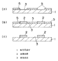
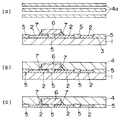
このような転写用基材1に対して金属皮膜2を形成するにあたっては、例えば図1に示すように、転写用基材1の被処理面3に適宜のパターン形状を有するめっきレジスト皮膜5を形成した後、無電解めっき処理と電解めっき処理の少なくとも一方にてめっき皮膜を形成し、これにより金属皮膜2を形成することができる。
【0045】
めっきレジスト皮膜5としては適宜のものを形成することができるが、例えばアクリル系やメタクリル系等の感光性樹脂組成物からなるものを用いることができる。
【0046】
金属皮膜2の材質は特に制限されないが、配線板製造時の導体配線の転写用に適用する場合には、銅めっき皮膜、銅めっきとニッケルめっきを順次施した銅・ニッケルめっき皮膜、銅めっき、金めっき、ニッケルめっきを順次施した銅・金・ニッケルめっき皮膜等を形成することが好ましい。配線板製造時の導体配線の転写用以外の用途に用いる場合には、めっきによる皮膜形成可能な金属皮膜2でれば特に制限はない。
【0047】
金属皮膜2の厚みは特に制限されないが、一般的な金属箔の厚みと同等な1〜150μmの範囲とすることが好ましい。また金属皮膜2の厚みを1μm未満とし、樹脂層4への金属皮膜2の転写後にこの金属皮膜2にめっき処理を施すことで厚膜化することもできる。また金属皮膜2の厚みが150μmを超えると、金属皮膜2の形成に時間がかかりすぎて処理コストも増大するものであり、まためっき皮膜も厚膜とする必要があり、めっき皮膜に十分な厚みがなければ金属皮膜2がその上部が盛り上がったキノコ状に形成されてしまう。また特に金属皮膜2の厚みは10〜35μmとすることが好ましく、この場合、被処理面3を銅イオンを含有するエッチング液による表面処理にて形成する場合は銅イオンを1〜3重量%の範囲で含有するエッチング液を用いることが好ましい。
【0048】
また転写用基材1に設けられた金属皮膜2には、その表面に黒化処理、サンドブラスト処理、アルカリ−亜塩素酸系黒化処理、ホーニング等のような、物理研磨、化学研磨等により、金属皮膜2に密着性付与のための表面処理を施すことにより、転写時における樹脂層4と金属皮膜2との密着性を向上することが好ましい。このようにすると、特に配線板用途において、長期信頼性を向上することができる。
【0049】
上記のようにしてめっき処理により転写用基材1に金属皮膜2を形成する際には、図1(c)に示すように金属皮膜2の形成後にめっきレジスト皮膜5を剥離するが、めっきレジスト皮膜5を転写用基材1に残存させ、樹脂層4に金属皮膜2を転写する際に同時にめっきレジスト皮膜5も樹脂層4に転写することもできる。詳しくは後述する。
【0050】
上記のようにして構成される転写用基材1を用いると、適宜の樹脂層4に対して金属皮膜2を転写することができ、特に配線板の製造にあたって導体配線を転写するために好適に用いることができるが、このような用途に限られず、配線板以外の電気機器に導体配線を転写したり、あるいは金属皮膜2による装飾を形成したりするためなど、種々の用途に適用することができる。
【0051】
上記のように構成される転写用基材1を用いた金属皮膜2の転写方法について、特に配線板を形成する場合に樹脂層4に導体配線を形成する場合を例に挙げて説明する。
【0052】
樹脂層4は、エポキシ樹脂組成物等のような適宜の電気絶縁性の熱硬化性樹脂組成物から構成することができる。
【0053】
樹脂層4の形成には、例えば樹脂組成物をシート状に成形し、加熱乾燥して半硬化状態とした樹脂シートや、繊維シートに樹脂組成物を含浸させ加熱乾燥して半硬化状態としたプリプレグなどといった、Bステージ状態の電気絶縁性の樹脂組成物から構成されるシート材を用いることができる。樹脂層4は一枚のシート材にて形成し、又は複数枚のシート材を積層一体化して形成することができる。
【0054】
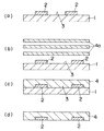
そして金属皮膜2が設けられた転写用基材1を金属皮膜2と樹脂層4とが対向するようにして樹脂層4に積層し、転写用基材1のみを剥離して金属皮膜2を樹脂層4側に残存させることにより、金属皮膜2を樹脂層4に転写して導体配線を形成し、配線板を得ることができる。
【0055】
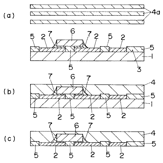
図2に示す例では、めっきレジスト皮膜5を剥離した転写用基材1を用い、まず一枚のシート材4a又はシート材4aを複数枚積層したものの一面又は両面に、金属皮膜2の形成がなされた転写用基材1を、金属皮膜2を形成した面がシート材4aと対向するように積層配置して加熱加圧成形を行うことにより一体化するものである。この加熱加圧成形は、成形後のシート材4aから形成される樹脂層4がBステージ状態に維持される条件又は樹脂層4がCステージ状態に形成される条件で行う。
【0056】
次いで、転写用基材1を樹脂層4から剥離すると共に、金属皮膜2を樹脂層4に残存させるものであり、これにより、樹脂層4(絶縁層)の一面又は両面に金属皮膜2からなる導体配線が設けられた配線板を得ることができる。
【0057】
このように形成される配線板では、樹脂層4(絶縁層)の片側又は両側の表層に、金属皮膜2からなる導体配線が樹脂層4(絶縁層)の表面に露出するように埋設されて形成されており、樹脂層4(絶縁層)の外面と導体配線の露出面とが面一となって、表面が凹凸なく平坦に形成される。
【0058】
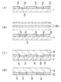
図3に示す例では、金属皮膜2の形成後にめっきレジスト皮膜5を剥離せずに残存させた転写用基材1を用い、まず一枚のシート材4a又はシート材4aを複数枚積層したものの一面又は両面に、金属皮膜2の形成がなされた転写用基材1を、金属皮膜2を形成すると共にめっきレジスト皮膜5を残存させた面がシート材4aと対向するように積層配置して加熱加圧成形を行うことにより一体化するものである。この加熱加圧成形は、成形後のシート材4aから形成される樹脂層4がBステージ状態に維持される条件又は樹脂層4がCステージ状態に形成される条件で行う。
【0059】
ここで、このようにめっきレジスト皮膜5を残存させたまま積層成形を行う場合には、めっきレジスト皮膜5を、プリント配線板用途に用いられる適宜の永久レジストで形成することが好ましく、例えばタムラ化研製のDSRシリーズ、アサヒ化研製のDPRシリーズ、太陽インキ製のPSRシリーズ等を用いることができる。
【0060】
次いで、転写用基材1を金属皮膜2及びめっきレジスト皮膜5から剥離すると共に、金属皮膜2とめっきレジスト皮膜5とを樹脂層4に残存させるものであり、これにより、絶縁層の一面又は両面に金属皮膜2からなる導体配線が設けられた配線板を得ることができる。
【0061】
このように形成される配線板では、樹脂層4と、これに密着して一体に成形されためっきレジスト皮膜5とから絶縁層が形成され、この絶縁層の片側又は両側の表層に、金属皮膜2からなる導体配線が絶縁層の表面に露出するように埋設されて形成されており、絶縁層の外面と導体配線の露出面とが面一となって、表面が凹凸なく平坦に形成される。このとき、樹脂層4に対する金属皮膜2の転写時には樹脂層4を構成する樹脂が大きく流動することがなく、成形性が更に向上する。
【0062】
また転写用基材1を剥離した後に、更にめっきレジスト皮膜5を樹脂層4から剥離することにより配線板を得るようにしても良い。この場合、樹脂層4からなる絶縁層の一面又は両面に、金属皮膜2からなる導体配線が凸状に形成された配線板が得られる。
【0063】
上記のようにして作製された配線板には、レーザ加工やドリル加工等による孔あけ加工を施した後に、この孔内にホールめっきを施したり導電性ペーストを充填したりするなどしてスルーホールを形成することができる。また金属皮膜2の転写前に予め樹脂層4に孔あけ加工を施すと共にこの孔内に導電性ペーストを充填し、次いでこの導電性ペーストを充填した孔の金属皮膜2とを位置合わせするようにして金属皮膜2を樹脂層4に転写することにより配線板を形成することもできる。
【0064】
また、配線板を作製するにあたっては、転写用基材1を形成した金属皮膜2の所定位置に電気部品6を実装した状態で樹脂層4に金属皮膜2を転写することにより、絶縁層内に電気部品6が埋設された配線板を作製することもできる。さらにこのように作製する配線板は、転写用基材1を用いることで、絶縁層内に電気部品6を所定位置に高精度に埋設することができる。
【0065】
図4に示す例では、転写用基材1を形成した金属皮膜2の所定位置に電気部品6を実装する。この電気部品6としては、チップ状抵抗体、チップ状コンデンサ、チップ状インダクタ等のような受動部品を実装することができるものであり、このときチップ状部品は半田7にて金属皮膜2に接続して実装することができる。また電気部品6としては、シリコンベアチップ等の半導体ベアチップのような能動部品を実装することもでき、この場合は、半導体ベアチップを半田ボール等により金属皮膜2に接続し、アンダーフィルを充填硬化して実装することができる。アンダーフィルとしては、一般的に用いられるエポキシ樹脂組成物等からなるものを用いることができる。
【0066】
尚、電気部品6の実装は半田7によるものには限られず、導電性ペーストを用いて実装することもできるが、半田7による接続の方が実装信頼性が高い。
【0067】
また、電気部品6を実装するにあたり、金属皮膜2が形成された転写用基材1上の所定箇所に、電気部品6として抵抗素子及びコンデンサ素子の少なくともいずれかを印刷成形することもできる。例えば抵抗素子(印刷抵抗)を印刷成形する場合には、熱硬化性樹脂中に金属粉を混入するなどしたペースト状の抵抗材料を印刷した後、加熱することにより、高容量の素子を形成することができる。またコンデンサ素子を印刷成形する場合には熱硬化性樹脂中に高誘電率フィラーとして、チタン酸バリウム等を混入するなどしたペースト状の誘電材料を印刷した後、加熱することにより高容量の素子を形成することができる。特に、ペーストの樹脂分を焼成して揮散させることによりセラミック状にして、より高い誘電素子を形成することができる。
【0068】
このように電気部品6を印刷成形する場合には、非常に薄い素子を形成することが可能になり薄型化を実現できる。また、電気部品6を半田実装することがないので、プリント配線板加工の既存設備での加工が可能となる。
【0069】
また、印刷成形された電気部品6に対しては、レーザによるトリミング等により容量値や抵抗値の調整が行われるが、この場合、FR−4タイプ等の配線板上に直接印刷成形する場合、熱による基板の破損や、熱収縮、熱劣化等による基板の信頼性低下などの、悪影響が生じるおそれがある。これに対して、電気部品6を転写用基材1上に印刷成形すると、電気部品6を転写用基材1上に実装した状態でレーザ加工を施すことができ、下地の破損や配線板シート材本体に対する熱による悪影響等を考慮せずに加工を行うことができるものである。
【0070】
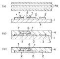
このように金属皮膜2に電気部品6が実装された転写用基材1を用いて、配線板を作製するにあたっては、まず一枚のシート材4a又はシート材4aを複数枚積層したものの一面又は両面に、金属皮膜2の形成がなされると共にこの金属皮膜2に電気部品6が実装された転写用基材1を、金属皮膜2を形成すると共に電気部品6が実装された面がシート材4aと対向するように積層配置して加熱加圧成形を行うことにより一体化するものである。この加熱加圧成形は、成形後のシート材4aから形成される樹脂層4がBステージ状態に維持される条件又は樹脂層4がCステージ状態に形成される条件で行う。
【0071】
この成形過程においては、まずシート材4aが溶融軟化すると共に複数のシート材4aが積層されている場合にはこれらのシート材4aが一体化し、またこの溶融軟化したシート材4aが流動することにより、転写用基材1に形成された金属皮膜2及び金属皮膜2に実装された電気部品6が、シート材4aから形成される樹脂層4中に埋設される。
【0072】
次いで、転写用基材1を樹脂層4から剥離すると共に、金属皮膜2を樹脂層4に残存させるものであり、これにより、樹脂層4(絶縁層)の一面又は両面に金属皮膜2からなる導体配線が設けられ、且つ絶縁層内に電気部品6が埋設された配線板を得ることができる。
【0073】
このように形成される配線板では、樹脂層4(絶縁層)の片側又は両側の表層に、金属皮膜2からなる導体配線が樹脂層4(絶縁層)の表面に露出するように埋設されて形成されており、樹脂層4(絶縁層)の外面と導体配線の露出面とが面一となって、表面が凹凸なく平坦に形成される。
【0074】
図5に示す例では、図3に示すものと同様に金属皮膜2の形成後にめっきレジスト皮膜5を剥離せずに残存させた転写用基材1を用い、この金属皮膜2の所定位置に、図4に示すものと同様に電気部品6を実装する。尚、図5に示す例では、めっきレジスト皮膜5の厚みよりも金属皮膜2の厚みを薄く形成しており、このときめっきレジスト皮膜5がアンダーフィルの役割を果たしている。
【0075】
そして、まず一枚のシート材4a又はシート材4aを複数枚積層したものの一面又は両面に、金属皮膜2の形成がなされた転写用基材1を、金属皮膜2を形成すると共にめっきレジスト皮膜5を残存させた面がシート材4aと対向するように積層配置して加熱加圧成形を行うことにより一体化するものである。この加熱加圧成形は、成形後のシート材4aから形成される樹脂層4がBステージ状態に維持される条件又は樹脂層4がCステージ状態に形成される条件で行う。
【0076】
この成形過程においては、まずシート材4aが溶融軟化すると共に複数のシート材4aが積層されている場合にはこれらのシート材4aが一体化し、またこの溶融軟化したシート材4aが流動することにより、転写用基材1に形成された金属皮膜2に実装された電気部品6が、シート材4aから形成される樹脂層4中に埋設される。また転写用基材1に残存させためっきレジスト皮膜5は、樹脂層4と積層一体化する。
【0077】
次いで、転写用基材1を金属皮膜2及びめっきレジスト皮膜5から剥離すると共に、金属皮膜2とめっきレジスト皮膜5とを樹脂層4に残存させるものであり、これにより、絶縁層の一面又は両面に金属皮膜2からなる導体配線が設けられ、且つ絶縁層内に電気部品6が埋設された配線板を得ることができる。
【0078】
このように形成される配線板では、樹脂層4と、これに密着して一体に成形されためっきレジスト皮膜5とから絶縁層が形成され、この絶縁層の片側又は両側の表層に、金属皮膜2からなる導体配線が絶縁層の表面に露出するように埋設されて形成されており、絶縁層の外面と導体配線の露出面とが面一となって、表面が凹凸なく平坦に形成される。
【0079】
このようにして形成された、絶縁層に電気部品6が埋設された配線板には、レーザ加工やドリル加工等による孔あけ加工を施した後に、この孔内にホールめっきを施したり導電性ペーストを充填したりするなどしてスルーホールを形成することができる。また金属皮膜2の転写前に予め樹脂層4に孔あけ加工を施すと共にこの孔内に導電性ペーストを充填し、次いでこの導電性ペーストを充填した孔の金属皮膜2とを位置合わせするようにして金属皮膜2を樹脂層4に転写することにより配線板を形成することもできる。
【0080】
以上のようにして得られる配線板は、絶縁層をCステージ状態まで硬化させる場合には、一層の絶縁層の片面又は両面に導体配線を有する配線板として用いられる。またこの配線板をコア材としてビルドアップ工法等により、更に多層の配線板を作製することもできる。
【0081】
また、絶縁層をBステージ状態に維持し、又はCステージ状態まで硬化させた配線板の一面又は両面に、絶縁層をBステージ状態に維持した他の配線板を積層し、加熱硬化することにより一体成形して、多層の配線板を得ることもできる。
【0082】
【実施例】
(実施例1)
ステンレス材として、SUS301(76%Fe,17%Cr,7%Ni)、調質3/4H、厚み100μmのものを用い、その一面に対して、3.0重量%の銅イオンを含有する塩化第二鉄溶液(酸化還元電位550mV、比重1.46)にてエッチング処理を15秒間施すことにより被処理面を形成し、転写用基材を得た。
【0083】
この転写用基材の被処理面の水洗、脱脂を行った後、被処理面にレジスト用感光性樹脂組成物(デュポン社製、品番「FX−140」)を塗布し、露光・現像処理を施すことによりめっきレジスト皮膜を形成した。次いで、7%塩酸水溶液を用いて45秒間酸処理を施した後、電解銅めっき(硫酸銅めっき)処理を施して、厚み10μmの金属皮膜を形成し、続いてめっきレジスト皮膜を剥離した。
【0084】
(実施例2)
被処理面の形成のためのエッチング処理を、8.0重量%の銅イオンを含有する塩化第二鉄溶液(酸化還元電位550mV、比重1.46)を用いて行い、その処理時間を5秒間とした。それ以外は実施例1と同様にして転写用基材に金属皮膜を形成した。
【0085】
(実施例3)
被処理面の形成のためのエッチング処理を、1.0重量%の銅イオンを含有する塩化第二鉄溶液(酸化還元電位555mV、比重1.46)を用いて行い、その処理時間を40秒間とした。それ以外は実施例1と同様にして転写用基材に金属皮膜を形成した。
【0086】
(実施例4)
被処理面の形成のためのエッチング処理を、3.0重量%の銅イオンを含有する塩化第二鉄溶液(酸化還元電位545mV、比重1.46)を用いて行い、その処理時間を40秒間とした。また形成する金属皮膜の厚みは35μmとなるようにした。それ以外は実施例1と同様にして転写用基材に金属皮膜を形成した。
【0087】
(実施例5)
使用するステンレス材の厚みを50μmとし、また形成する金属皮膜の厚みは50μmとなるようにした。それ以外は実施例1と同様にして転写用基材に金属皮膜を形成した。
【0088】
(実施例6)
使用するステンレス材の厚みを200μmとし、また形成する金属皮膜の厚みは50μmとなるようにした。それ以外は実施例1と同様にして転写用基材に金属皮膜を形成した。
【0089】
(実施例7)
被処理面の形成のためのエッチング処理を、3.0重量%の銅イオンを含有する塩化第二鉄溶液(酸化還元電位552mV、比重1.46)を用いて行い、その処理時間を40秒間とした。また形成された金属皮膜の表面には、黒化処理を施した。それ以外は実施例1と同様にして転写用基材に金属皮膜を形成した。
【0090】
(実施例8)
めっきレジスト皮膜を、耐金めっき性を有する永久レジスト(タムラ化研製、品番「DSR 2200KGX−88」)にて厚み9μmに形成した。また金属皮膜の形成にあたっては、硫酸銅めっき処理にて厚み10μmの皮膜を形成した後、厚み5μmのニッケルめっきの皮膜と厚み0.5μmの金めっきの皮膜を形成した。また転写用基材にはめっきレジスト皮膜を剥離せずに残存させた。それ以外は実施例1と同様にして転写用基材に金属皮膜を形成した。
【0091】
(実施例9)
ステンレス基材として、SUS304(74%Fe,18%Cr,8%Ni)、調質3/4H、厚み100μmのものを用いた以外は、実施例1と同様にして、転写用基材に金属皮膜を形成した。
【0092】
(実施例10)
ステンレス基材として、SUS316(67.5%Fe,18%Cr,12%Ni,2.5%Mo)、調質H、厚み100μmのものを用いた以外は、実施例1と同様にして、転写用基材に金属皮膜を形成した。
【0093】
(実施例11)
ステンレス基材として、SUS631−CSP(75%Fe,17%Cr,7%Ni,1%Al)、調質H、厚み100μmのものを用いた以外は、実施例1と同様にして、転写用基材に金属皮膜を形成した。
【0094】
(実施例12)
被処理面の形成のためのエッチング処理を、0.08重量%の銅イオンを含有する塩化第二鉄溶液(酸化還元電位555mV、比重1.46)を用いて行い、その処理時間を120秒間とした。また形成された金属皮膜の表面には、黒化処理を施した。それ以外は実施例1と同様にして転写用基材に金属皮膜を形成した。
【0095】
(実施例13)
被処理面の形成のためのエッチング処理を、3重量%のニッケルイオンを含有する塩化第二鉄溶液(酸化還元電位550mV、比重1.45)を用いて行い、その処理時間を40秒間とした。また形成された金属皮膜の表面には、黒化処理を施した。それ以外は実施例1と同様にして転写用基材に金属皮膜を形成した。
【0096】
(比較例1)
ステンレス材に被処理面を形成しないものを転写用基材として用いた以外は実施例1と同様にして、転写用基材に金属皮膜を形成した。
【0097】
(比較例2)
ステンレス材に対するエッチング処理を、銅イオンを含有しない塩化第二鉄溶液(酸化還元電位560mV、比重1.45)を用いて行い、その処理時間を40秒間とした。それ以外は実施例1と同様にして転写用基材に金属皮膜を形成した。
【0098】
(比較例3)
ステンレス基材として、SUS304(74%Fe,18%Cr,8%Ni)、調質3/4H、厚み100μmのもの(実施例9と同様のもの)を用い、ステンレス材に対するエッチング処理を、銅イオンを含有しない塩化第二鉄溶液(酸化還元電位560mV、比重1.46)を用いて行い、その処理時間を40秒間とした。それ以外は実施例1と同様にして転写用基材に金属皮膜を形成した。
【0099】
(比較例4)
ステンレス材に対してエッチング処理を施す代わりに、#1500のサンドペーパにて研磨することにより粗化して転写用基材を形成し、この粗化面に対して金属皮膜を形成するようにした。それ以外は実施例1と同様にして転写用基材に金属皮膜を形成した。
【0100】
(比較例5)
ステンレス材に対してエッチング処理を施す代わりに、#100のサンドペーパにて研磨することにより粗化して転写用基材を形成し、この粗化面に対して金属皮膜を形成するようにした。それ以外は実施例1と同様にして転写用基材に金属皮膜を形成した。
【0101】
(評価試験)
1.表面粗度測定
各実施例及び比較例につき、金属皮膜が設けられている側の転写用基材の面の表面粗度Raを、JIS B0601に基づき、触針式の小型表面粗さ測定器(ハンディーサーフ;型番「E−35A」;東京精密社製)を用いて、カットオフ値λc=0.80mm、測定長さL=λc×5=4.0mmで測定した。
【0102】
2.半田耐熱性試験
各実施例及び比較例につき、転写用基材に設けた金属皮膜を、260℃のリフロー炉にて20秒間加熱した後の、転写用基材からの金属皮膜の剥離の有無を観察し、次のような評価基準で評価した。
○:剥離発生なし。×:浮き剥離発生。−:リフロー処理前に剥離発生していて判定不可。
【0103】
3.ピール強度評価及び転写性評価
各実施例及び比較例につき、まずフィラー85重量%含有させた熱硬化性エポキシ樹脂を使用した松下電工株式会社製の樹脂付き銅箔(品番「R−0870」)における樹脂の厚みを400μmに変更し、この樹脂付き銅箔の樹脂面に転写用基材6を、金属皮膜5を形成した面が樹脂シートと対向するように積層配置すると共に他面にステンレス箔を配置し、更にその両側に厚み75μmの離型性PETフィルム、厚み2mmのSUSプレート、2枚のパット紙をそれぞれ順次配置したものを、減圧チャンバー内で熱盤間に配置した。
【0104】
この状態で減圧チャンバー内を真空引きして1.3kPa(10Torr)以下の減圧雰囲気としてから加熱加圧成形を行った。成形は、まず130℃、29MPa(3kgf/cm2)で10分保持した後、15分間かけて175℃まで昇温し、この状態で10分間保持することにより行った。
【0105】
成形後、転写用基材のみを剥離する際におけるピール強度を、引っ張り試験機によるバネばかりの目視計測により測定した。
【0106】
また、転写用基材の剥離後の、樹脂層に転写された金属皮膜を観察し、次の評価基準にて転写性を評価した。
○:全て転写。△:転写するが実施しにくい。×:転写せず。−:転写前に金属皮膜が剥離して評価不能。
【0107】
以上の結果を表1に示す。
【0108】
【表1】
【発明の効果】
上記のように請求項1に係る転写用基材では、金属鉄を含有する金属材に形成された鉄よりもイオン化傾向が小さい金属を含有する被処理面は、金属めっき皮膜との間で適度な密着性と離型性を有し、転写用基材にめっき皮膜からなる金属皮膜を設けた場合に、金属皮膜の転写時に転写用基材に金属皮膜が残存しないようにすることができて良好な剥離性を有し、また金属皮膜を設けた転写用基材の取り扱い時等においては金属皮膜が転写用基材から不用意に剥離するようなことを防止することができるものである。
【0110】
また請求項2の発明では、鉄イオンと、鉄よりもイオン化傾向が小さい金属のイオンとを含有するエッチング液を用いることで、形成される被処理面に特に優れた密着性と離型性とを付与することができるものである。
【0111】
また請求項3の発明では、塩化第二鉄、又は塩化第二鉄及び塩化第一鉄を含有すると共に銅及びニッケルのうち少なくとも一方の金属のイオンを0.01〜20重量%の濃度で含有するエッチング液を用いることで、特に金属皮膜として銅めっき皮膜を形成する場合に、形成される被処理面に更に優れた密着性と離型性とを付与することができるものである。
【0112】
また請求項4の発明では、ステンレス材を用いることで、ステンレス材は入手容易であるため、製造コスト削減が可能なものである。
【0113】
また請求項5の発明では、表面粗度Raが0.05〜1.00μmの被処理面によって特に優れた密着性と離型性とを付与することができるものである。
【0114】
また請求項6の発明では、クロム含有率が10〜20%、ニッケル含有率が0〜15%の、金属鉄を含有する金属材により、被処理面に表面粗化処理を施す場合に粗化容易となるようにすることができるものである。
【0115】
また請求項7の発明では、銅、銅及びニッケル、銅及びニッケル及び金、又はニッケルからなるめっき皮膜による金属皮膜により、特に配線板の導体配線形成用途に好適に用いることができるものである。
【0116】
また請求項8の発明は、めっき皮膜による金属皮膜の転写時における樹脂層と金属皮膜との密着性を、金属皮膜の表面に密着性付与のための表面処理を施すことで向上することができ、特に配線板用途において、長期信頼性を向上することができるものである。
【0117】
また請求項9の発明は、被処理面にめっきレジスト皮膜を形成した後にめっき処理を施すことで、めっき処理により被処理面に金属皮膜を形成することができるものである。
【0118】
また請求項10の発明は、金属皮膜を厚み1〜150μmに形成することでその表面を平坦に形成すると共に処理コストの増大を抑制することができるものである。
【0119】
また請求項11の発明は、ばね性を有する金属鉄を含有する金属材により、転写用基材を剥離する際に撓ませたり応力をかけたりしても転写用基材に破損が生じにくくなり、使用後の転写用基材を洗浄して有機分の除去を行えば、再度めっき処理等により転写用基材に金属皮膜を設けて、転写用基材を繰り返し使用することが可能となり、材料コストを削減でき、また資源の有効活用により環境保護につながるものである。
【0120】
また請求項12の発明は、金属鉄を含有する金属材の厚みを20〜150μmとすることで、転写用基材を剥離する際に、転写用基材をめくりあげて撓ませながら容易に剥離することができ、且つこのとき樹脂層に対して過大な応力がかかることを抑制して樹脂層の破損等を防止することができるものである。
【0121】
また請求項13に係る配線板の製造方法では、金属皮膜の転写時に転写用基材に金属皮膜が残存しないようにすることができて良好な剥離性を有し、また金属皮膜を設けた転写用基材の取り扱い時等においては金属皮膜が転写用基材から不用意に剥離するようなことを防止することができるものである。
【0122】
また請求項14に係る配線板の製造方法では、金属皮膜の転写時に転写用基材に金属皮膜が残存しないようにすることができて良好な剥離性を有し、また金属皮膜を設けた転写用基材の取り扱い時等においては金属皮膜が転写用基材から不用意に剥離するようなことを防止することができるものである。
【図面の簡単な説明】
【図1】本発明の実施の形態の一例を示すものであり、(a)乃至(c)は概略断面図である。
【図2】配線板の製造工程の一例を示すものであり、(a)乃至(d)は概略断面図である。
【図3】配線板の製造工程の他例を示すものであり、(a)乃至(d)は概略断面図である。
【図4】配線板の製造工程の更に他例を示すものであり、(a)乃至(c)は概略断面図である。
【図5】配線板の製造工程の更に他例を示すものであり、(a)乃至(c)は概略断面図である。
【符号の説明】
1 転写用基材
2 金属皮膜
3 被処理面
4 樹脂層
5 めっきレジスト皮膜
6 電気部品[0001]
BACKGROUND OF THE INVENTION
In the present invention, a transfer substrate having a metal film on the surface is laminated so that the metal film and the resin layer face the resin layer, and the transfer substrate is peeled off from the resin layer and the metal The present invention relates to a transfer substrate used for transferring a metal film to a resin layer by allowing the film to remain on the resin layer side, and a method of manufacturing a wiring board in which conductor wiring is formed on the resin layer using the transfer substrate. Is.
[0002]
[Prior art]
In recent years, with the demand for higher functionality and smaller size and thinner electronic devices, there has been a demand for shorter wiring distances and smaller printed wiring boards.
[0003]
The demand for such wiring boards has become difficult to cope with by forming conductor wiring by applying additive and subtractive methods to laminated boards, and new techniques for forming conductor wiring are required. It was.
[0004]
As one of the proposals for such a new conductor wiring formation technology, a conductor wiring is formed by plating or the like on the surface of a transfer substrate such as a stainless steel plate whose surface is roughened. There is a method of transferring and embedding a conductor wiring in a resin layer by laminating a conductor wiring of a transfer substrate and an adhesive resin layer facing each other, and then peeling only the transfer substrate (Patent Document 1). .
[0005]
[Patent Document 1]
Japanese Patent No. 3241505 (FIG. 1)
[0006]
[Problems to be solved by the invention]
However, in the method disclosed in
[0007]
In addition, as a technique for controlling adhesion by metal surface treatment, for example, as disclosed in Japanese Patent Application Laid-Open No. 11-293576 and Japanese Patent Application Laid-Open No. 2002-53977, chemicals that involve film formation on a metal surface After etching treatment, this film is chemically removed to roughen the surface, and if necessary, a method to form a film on the metal surface has been proposed. Although it is possible to reduce the adhesion by changing the processing conditions such as reducing the concentration of the processing chemical solution, it is a special process, so the processing cost becomes very high. There was a problem.
[0008]
The present invention has been made in view of the above points, and the transfer base material provided with a metal film on the surface is laminated so that the metal film and the resin layer face the resin layer, When transferring the metal film to the resin layer by peeling the transfer substrate from the resin layer and leaving the metal film on the resin layer side, the transfer substrate is provided with appropriate adhesion and peelability by a simple process. In particular, it is intended to provide a transfer base material suitably used for transfer molding of conductor wiring on a wiring board, and a method of manufacturing a wiring board using the transfer base material. is there.
[0009]
[Means for Solving the Problems]
The transfer substrate according to
[0010]
According to a second aspect of the present invention, in the first aspect, the surface of the metal material containing metallic iron is subjected to surface treatment using an etching solution containing iron ions and metal ions having a smaller ionization tendency than iron. Thus, a surface to be processed is formed, and thereby, particularly excellent adhesion and releasability can be imparted to the
[0011]
A third aspect of the present invention is that, in the second aspect, the etching solution contains ferric chloride, or ferric chloride and ferrous chloride, and copper and nickel as metals having a smaller ionization tendency than iron. Of these, at least one metal ion is contained at a concentration of 0.01 to 20% by weight. With this, particularly when a copper plating film is formed as the
[0012]
The invention of
[0013]
According to a fifth aspect of the present invention, in any one of the first to fourth aspects, the surface roughness Ra of the surface to be processed 3 is 0.05 to 1.00 μm. The
[0014]
The invention of
[0015]
A seventh aspect of the present invention is the metal film according to any one of the first to sixth aspects, wherein the surface to be treated 3 is a metal film formed of any one of copper, copper and nickel, copper, nickel and gold, and nickel. In this way, it can be suitably used particularly for a conductor wiring forming application of a wiring board.
[0016]
The invention of claim 8 is the method according to any one of
[0017]
A ninth aspect of the present invention is the method according to any one of the first to eighth aspects, wherein after the plating resist
[0018]
The invention of
[0019]
The invention of claim 11 is characterized in that, in any one of
[0020]
The invention of claim 12 is characterized in that, in any one of
[0021]
The method for manufacturing a wiring board according to claim 13 is characterized in that the substrate for
[0022]
According to a fourteenth aspect of the present invention, there is provided a method of manufacturing a wiring board according to the thirteenth aspect, wherein the
[0023]
DETAILED DESCRIPTION OF THE INVENTION
Embodiments of the present invention will be described below.
[0024]
The substrate for
[0025]
As the metal material containing this metallic iron, an appropriate material is used, but in order to facilitate the roughening particularly when the surface roughening treatment is performed, the chromium content is preferably 10 to 20%, A nickel content of 0 to 15% is used. Examples of such a metal material containing metallic iron include an appropriate stainless steel material such as one made of SUS301 or SUS304. Surface roughening is possible with other materials, but it becomes difficult to control the concentration of the etching solution for the roughening treatment. Moreover, since the stainless steel materials having these compositions are widely used and easily available, manufacturing costs can be reduced.
[0026]
Moreover, it is preferable to use a metal material containing metallic iron having spring properties. Examples of the metal material containing metallic iron having spring properties include a stainless steel band for springs defined in JIS G 4313, and examples thereof include SUS301-CSP and SUS631-CSP. When such a metal material containing metallic iron is used, the
[0027]
In order to improve peelability, the thickness of the metal material containing metallic iron is preferably in the range of 20 to 150 μm. In this case, when the
[0028]
And the
[0029]
In producing the
[0030]
In addition, by treating one surface of the stainless steel material with an etching solution, the surface of the metal material containing metallic iron can be roughened, and at the same time, the surface to be treated 3 can be formed on this surface. At this time, as the etching solution, the metal solution contains metal iron by treating one surface of the metal material containing metal iron using an etching solution containing iron ions and metal ions having a smaller ionization tendency than iron. The surface to be treated 3 can be formed by applying a roughening treatment to the surface of the metal material and simultaneously containing a metal having a smaller ionization tendency than iron on the surface.
[0031]
This etchant contains ferric chloride, or an alkaline etchant (iron chloride etchant) containing ferric chloride and ferrous chloride to contain iron ions, which is more ionized than iron. It is preferable to use a metal ion containing a small metal ion, and it is preferable to contain a copper ion or a nickel ion as the metal ion having a smaller ionization tendency than iron.
[0032]
Here, for processing of a normal stainless steel material or the like, an etching solution having an oxidation-reduction potential of 660 mV or more is used to perform processing with less side etching. The purpose is to form irregularities that improve the properties, and it is preferable to perform the treatment with an etching solution having a lower redox potential than ordinary stainless steel processing in order to only roughen the surface. Specifically, as an alkaline etching solution containing ferric chloride or containing ferric chloride and ferrous chloride, the specific gravity is 1.1 to 1.7, and the redox potential is 400. It is preferable to use one in the range of ˜660 mV.
[0033]
If such an etching solution is used as a surface treatment solution for a metal material containing metallic iron, the following two reactions mainly occur simultaneously on the metal surface containing metallic iron, which is considered to enable surface treatment. .
[0034]
The first reaction is a reaction for roughening a metal surface containing metallic iron as shown below.
[0035]
2FeCl3+ Fe → 3FeCl2
That is, it is a reaction that etches iron, which is a main component of a metal material containing metallic iron. This is generally considered to be a reaction in which iron reacts with trivalent iron ions in the solution to become divalent iron ions and dissolves. It should be noted that, in the sense of dissolving iron, it is preferable that the oxidation-reduction potential of a general etching solution is as high as 660 to 700 mV. In such a case, since only the surface treatment of the metal material containing metallic iron is required, it is preferable to use an etching solution having a weak etching power of 400 to 660 mV, thereby containing metallic iron. Surface roughness can be achieved with almost no change in the thickness of the metal material before and after treatment.
[0036]
The second reaction is a reaction in which a metal having a smaller ionization tendency than iron such as copper is attached to the surface of a metal material containing metallic iron as shown below. The following formula is for the case where copper ions are contained by containing copper chloride in the etching solution.
[0037]
CuCl2+ Fe → FeCl2+ Cu
In this reaction, a metal ion containing metal ions and metal iron having a smaller ionization tendency than iron in the liquid by containing metal ions having a smaller ionization tendency than iron such as copper ions in the etching solution. Reacts with iron, which is the main component of the material, and the iron is etched and ionized, but metal ions that have a lower ionization tendency than iron are deposited on the roughened surface of the metal material containing metal iron as a metal. It will be in the state of containing.
[0038]
By these two reactions, the surface to be treated 3 containing copper can be formed on the surface roughened surface of the metal containing metallic iron, and appropriate adhesion between the metal plating film, particularly the copper plating film. It is possible to have
[0039]
In the present invention, a conventional etching technique is formed by forming the surface to be processed 3 by using an etching solution containing a metal ion having a smaller ionization tendency than iron in a generally used iron chloride etching solution. It became possible for the first time to provide adhesion with a plating film that could not be obtained by simply roughening with. The specific gravity of the etching solution containing metal ions having a smaller ionization tendency than iron in the iron chloride etching solution is preferably 1.1 to 1.7, and the oxidation-reduction potential is preferably 400 to 660 mV. Thus, as will be described in detail later, even if the component is mounted on a metal film 2 (conductor wiring) formed by plating or the like on a metal material containing metallic iron by solder reflow, the
[0040]
In this way, when an etching solution containing ions of a metal having a smaller ionization tendency than iron is used in the iron chloride etching solution, the metal adheres to the roughened surface of the metal containing metal iron, and the object to be processed The
[0041]
When using an alkaline etching solution such as a ferric chloride solution in which ions of a metal having a smaller ionization tendency than iron are used as described above, a metal ion having a smaller ionization tendency than iron in the etching solution is used. The content of is preferably 0.01 to 20% by weight. If this content is less than 0.01% by weight, the
[0042]
The content of the metal having a smaller ionization tendency than iron in the surface to be processed 3 is not particularly limited, and is suitable according to processing conditions such as processing time required for roughening when performing processing using an etching solution. The amount of adhesion may also vary. For example, when the surface treatment is performed with an etching solution having a smaller ionization tendency than that of iron with a metal ion content, the treatment time is lengthened. When the surface treatment is performed with an etching solution having a high content, the treatment time is shortened. By changing the processing conditions such as, it is possible to obtain appropriate adhesion between the surface to be processed 3 and the metal plating film.
[0043]
Moreover, it is preferable to form the to-
[0044]
In forming the
[0045]
As the plating resist
[0046]
The material of the
[0047]
Although the thickness in particular of the metal membrane | film |
[0048]
Further, the
[0049]
When the
[0050]
When the
[0051]
The transfer method of the
[0052]
The
[0053]
For the formation of the
[0054]
Then, the
[0055]
In the example shown in FIG. 2, the
[0056]
Next, the
[0057]
In the wiring board thus formed, the conductor wiring made of the
[0058]
In the example shown in FIG. 3, the
[0059]
Here, when performing lamination molding with the plating resist
[0060]
Next, the
[0061]
In the wiring board formed in this way, an insulating layer is formed from the
[0062]
Further, after the
[0063]
The wiring board produced as described above is subjected to hole processing by laser processing, drilling, etc., and then plated with holes or filled with conductive paste in the holes. Can be formed. Before transferring the
[0064]
Further, when producing the wiring board, the
[0065]
In the example shown in FIG. 4, the
[0066]
Note that the mounting of the
[0067]
In mounting the
[0068]
In this way, when the
[0069]
In addition, for the printed and molded
[0070]
In producing a wiring board using the
[0071]
In this molding process, first, when the
[0072]
Next, the
[0073]
In the wiring board thus formed, the conductor wiring made of the
[0074]
In the example shown in FIG. 5, similarly to the case shown in FIG. 3, the
[0075]
First, the
[0076]
In this molding process, first, when the
[0077]
Next, the
[0078]
In the wiring board formed in this way, an insulating layer is formed from the
[0079]
The thus formed wiring board in which the
[0080]
The wiring board obtained as described above is used as a wiring board having conductor wiring on one side or both sides of a single insulating layer when the insulating layer is cured to the C stage state. Further, a multilayer wiring board can be produced by a build-up method using this wiring board as a core material.
[0081]
In addition, by stacking another wiring board that maintains the insulating layer in the B stage state on one or both sides of the wiring board that is maintained in the B stage state or cured to the C stage state, and heat-cured A multilayer wiring board can also be obtained by integral molding.
[0082]
【Example】
(Example 1)
As the stainless steel, SUS301 (76% Fe, 17% Cr, 7% Ni), tempered 3 / 4H, thickness 100 μm was used, and chloride containing 3.0% by weight of copper ions on one side thereof. A surface to be treated was formed by performing an etching treatment with a ferric solution (oxidation-reduction potential 550 mV, specific gravity 1.46) for 15 seconds to obtain a transfer substrate.
[0083]
After the surface to be treated of the transfer substrate is washed with water and degreased, a photosensitive resin composition for resist (manufactured by DuPont, product number “FX-140”) is applied to the surface to be treated, and exposure and development are performed. A plating resist film was formed by applying. Next, after performing an acid treatment for 45 seconds using a 7% hydrochloric acid aqueous solution, an electrolytic copper plating (copper sulfate plating) treatment was performed to form a metal film having a thickness of 10 μm, and then the plating resist film was peeled off.
[0084]
(Example 2)
Etching for forming the surface to be processed is performed using a ferric chloride solution (redox potential 550 mV, specific gravity 1.46) containing 8.0% by weight of copper ions, and the processing time is 5 seconds. It was. Otherwise, a metal film was formed on the transfer substrate in the same manner as in Example 1.
[0085]
(Example 3)
Etching for forming the surface to be processed is performed using a ferric chloride solution (oxidation-reduction potential 555 mV, specific gravity 1.46) containing 1.0% by weight of copper ions, and the processing time is 40 seconds. It was. Otherwise, a metal film was formed on the transfer substrate in the same manner as in Example 1.
[0086]
Example 4
Etching for forming the surface to be processed is performed using a ferric chloride solution (oxidation-reduction potential 545 mV, specific gravity 1.46) containing 3.0% by weight of copper ions, and the processing time is 40 seconds. It was. The thickness of the metal film to be formed was set to 35 μm. Otherwise, a metal film was formed on the transfer substrate in the same manner as in Example 1.
[0087]
(Example 5)
The thickness of the stainless steel used was 50 μm, and the thickness of the metal film to be formed was 50 μm. Otherwise, a metal film was formed on the transfer substrate in the same manner as in Example 1.
[0088]
(Example 6)
The thickness of the stainless steel used was 200 μm, and the thickness of the metal film to be formed was 50 μm. Otherwise, a metal film was formed on the transfer substrate in the same manner as in Example 1.
[0089]
(Example 7)
Etching for forming the surface to be processed is performed using a ferric chloride solution (oxidation-reduction potential 552 mV, specific gravity 1.46) containing 3.0% by weight of copper ions, and the processing time is 40 seconds. It was. Moreover, the surface of the formed metal film was blackened. Otherwise, a metal film was formed on the transfer substrate in the same manner as in Example 1.
[0090]
(Example 8)
A plating resist film was formed to a thickness of 9 μm using a permanent resist having a gold plating resistance (product number “DSR 2200KGX-88” manufactured by Tamura Kaken). In forming the metal film, a 10 μm thick film was formed by copper sulfate plating, and then a 5 μm thick nickel plated film and a 0.5 μm thick gold plated film were formed. Further, the plating resist film was left on the transfer substrate without peeling off. Otherwise, a metal film was formed on the transfer substrate in the same manner as in Example 1.
[0091]
Example 9
As a stainless steel base material, the same material as in Example 1 was used except that SUS304 (74% Fe, 18% Cr, 8% Ni), tempered 3 / 4H, and a thickness of 100 μm was used. A film was formed.
[0092]
(Example 10)
As a stainless steel base material, except that SUS316 (67.5% Fe, 18% Cr, 12% Ni, 2.5% Mo), tempered H, and a thickness of 100 μm were used, the same as in Example 1, A metal film was formed on the transfer substrate.
[0093]
(Example 11)
For transfer in the same manner as in Example 1 except that SUS631-CSP (75% Fe, 17% Cr, 7% Ni, 1% Al), tempered H, and thickness of 100 μm was used as the stainless steel substrate. A metal film was formed on the substrate.
[0094]
(Example 12)
Etching treatment for forming the surface to be treated is performed using a ferric chloride solution (oxidation-reduction potential 555 mV, specific gravity 1.46) containing 0.08% by weight of copper ions, and the treatment time is 120 seconds. It was. Moreover, the surface of the formed metal film was blackened. Otherwise, a metal film was formed on the transfer substrate in the same manner as in Example 1.
[0095]
(Example 13)
Etching treatment for forming the surface to be treated is performed using a ferric chloride solution (oxidation-reduction potential 550 mV, specific gravity 1.45) containing 3% by weight of nickel ions, and the treatment time is 40 seconds. . Moreover, the surface of the formed metal film was blackened. Otherwise, a metal film was formed on the transfer substrate in the same manner as in Example 1.
[0096]
(Comparative Example 1)
A metal film was formed on the transfer substrate in the same manner as in Example 1 except that a stainless steel material having no surface to be processed was used as the transfer substrate.
[0097]
(Comparative Example 2)
Etching treatment for the stainless steel material was performed using a ferric chloride solution (oxidation-reduction potential 560 mV, specific gravity 1.45) containing no copper ions, and the treatment time was 40 seconds. Otherwise, a metal film was formed on the transfer substrate in the same manner as in Example 1.
[0098]
(Comparative Example 3)
As the stainless steel substrate, SUS304 (74% Fe, 18% Cr, 8% Ni), tempered 3 / 4H, 100 μm thick (same as in Example 9) was used, and the etching treatment for the stainless steel material was performed using copper. This was carried out using a ferric chloride solution containing no ions (oxidation-reduction potential 560 mV, specific gravity 1.46), and the treatment time was 40 seconds. Otherwise, a metal film was formed on the transfer substrate in the same manner as in Example 1.
[0099]
(Comparative Example 4)
Instead of etching the stainless steel, it was roughened by polishing with # 1500 sand paper to form a transfer substrate, and a metal film was formed on the roughened surface. Otherwise, a metal film was formed on the transfer substrate in the same manner as in Example 1.
[0100]
(Comparative Example 5)
Instead of etching the stainless steel, it was roughened by polishing with # 100 sand paper to form a transfer substrate, and a metal film was formed on the roughened surface. Otherwise, a metal film was formed on the transfer substrate in the same manner as in Example 1.
[0101]
(Evaluation test)
1. Surface roughness measurement
For each of the examples and comparative examples, the surface roughness Ra of the surface of the transfer base on which the metal film is provided is determined based on JIS B0601, a stylus type small surface roughness measuring instrument (handy surf; model number) Cut-off value λ using “E-35A” (manufactured by Tokyo Seimitsu)c= 0.80 mm, measurement length L = λc× 5 = Measured at 4.0 mm.
[0102]
2. Solder heat resistance test
For each of the examples and comparative examples, the metal film provided on the transfer substrate was heated in a reflow oven at 260 ° C. for 20 seconds, and then observed for the peeling of the metal film from the transfer substrate. Evaluation was made according to the following evaluation criteria.
○: No peeling occurred. X: Floating peeling occurred. -: Separation occurred before reflow treatment, and determination is not possible.
[0103]
3. Peel strength evaluation and transferability evaluation
For each of the examples and comparative examples, the resin thickness of the resin-coated copper foil (product number “R-0870”) manufactured by Matsushita Electric Works, Ltd. using a thermosetting epoxy resin containing 85% by weight of filler was first changed to 400 μm. Then, the
[0104]
In this state, the inside of the reduced pressure chamber was evacuated to form a reduced pressure atmosphere of 1.3 kPa (10 Torr) or less, and then heat and pressure molding was performed. Molding is first performed at 130 ° C. and 29 MPa (3 kgf / cm2) For 10 minutes, then the temperature was raised to 175 ° C. over 15 minutes, and this state was maintained for 10 minutes.
[0105]
After molding, the peel strength when only the transfer substrate was peeled was measured by visual measurement of only the springs using a tensile tester.
[0106]
Further, the metal film transferred to the resin layer after the transfer substrate was peeled was observed, and the transferability was evaluated according to the following evaluation criteria.
○: All transferred. Δ: Transfer is difficult to implement. X: Not transferred. -: The metal film peels off before transfer and cannot be evaluated.
[0107]
The results are shown in Table 1.
[0108]
[Table 1]
【The invention's effect】
As described above, in the transfer substrate according to the first aspect, the surface to be treated containing a metal having a smaller ionization tendency than the iron formed on the metal material containing metal iron is moderate between the metal plating film. It has excellent adhesion and releasability, and when a metal film consisting of a plating film is provided on the transfer substrate, the metal film can be prevented from remaining on the transfer substrate when the metal film is transferred. It has good releasability and can prevent the metal film from being inadvertently peeled off from the transfer substrate when handling the transfer substrate provided with the metal film.
[0110]
Further, in the invention of
[0111]
The invention of
[0112]
In the invention of
[0113]
In the invention of
[0114]
Further, in the invention of
[0115]
Further, in the invention of
[0116]
The invention of claim 8 can improve the adhesion between the resin layer and the metal film during the transfer of the metal film by the plating film by applying a surface treatment for imparting adhesion to the surface of the metal film. In particular, long-term reliability can be improved in wiring board applications.
[0117]
According to the ninth aspect of the present invention, a metal film can be formed on the surface to be treated by plating by forming a plating resist film on the surface to be treated and then performing a plating treatment.
[0118]
In the invention of
[0119]
According to the invention of claim 11, even if the transfer base material is bent or stressed when the transfer base material is peeled off, the transfer base material is less likely to be damaged by the metal material containing metallic iron having a spring property. If the transfer substrate after use is washed to remove the organic component, the transfer substrate can be used repeatedly by providing a metal film on the transfer substrate again by plating, etc. Costs can be reduced, and effective use of resources leads to environmental protection.
[0120]
In the invention of claim 12, when the thickness of the metal material containing metallic iron is 20 to 150 μm, when the transfer substrate is peeled off, the transfer substrate is turned up and bent easily while being bent. In this case, the resin layer can be prevented from being damaged by preventing an excessive stress from being applied to the resin layer.
[0121]
Further, in the method for manufacturing a wiring board according to claim 13, the metal film can be prevented from remaining on the transfer substrate during the transfer of the metal film, has a good releasability, and is provided with the metal film. It is possible to prevent the metal film from being inadvertently peeled off from the transfer substrate when handling the transfer substrate.
[0122]
Further, in the method for manufacturing a wiring board according to claim 14, the metal film can be prevented from remaining on the transfer substrate at the time of transferring the metal film, has a good releasability, and is provided with a metal film. It is possible to prevent the metal film from being inadvertently peeled off from the transfer substrate when handling the transfer substrate.
[Brief description of the drawings]
FIG. 1 shows an example of an embodiment of the present invention, and (a) to (c) are schematic cross-sectional views.
FIG. 2 shows an example of a manufacturing process of a wiring board, and (a) to (d) are schematic cross-sectional views.
FIG. 3 shows another example of the manufacturing process of the wiring board, and (a) to (d) are schematic cross-sectional views.
FIG. 4 shows still another example of the manufacturing process of the wiring board, and (a) to (c) are schematic cross-sectional views.
FIG. 5 shows still another example of the manufacturing process of the wiring board, and (a) to (c) are schematic cross-sectional views.
[Explanation of symbols]
1 Transfer substrate
2 Metal coating
3 Surface to be treated
4 Resin layer
5 Plating resist film
6 Electrical parts
Claims (14)
Priority Applications (1)
| Application Number | Priority Date | Filing Date | Title |
|---|---|---|---|
| JP2003149809A JP3894162B2 (en) | 2002-11-26 | 2003-05-27 | Substrate for transfer and method for producing wiring board |
Applications Claiming Priority (2)
| Application Number | Priority Date | Filing Date | Title |
|---|---|---|---|
| JP2002342915 | 2002-11-26 | ||
| JP2003149809A JP3894162B2 (en) | 2002-11-26 | 2003-05-27 | Substrate for transfer and method for producing wiring board |
Publications (2)
| Publication Number | Publication Date |
|---|---|
| JP2004228551A true JP2004228551A (en) | 2004-08-12 |
| JP3894162B2 JP3894162B2 (en) | 2007-03-14 |
Family
ID=32910879
Family Applications (1)
| Application Number | Title | Priority Date | Filing Date |
|---|---|---|---|
| JP2003149809A Expired - Fee Related JP3894162B2 (en) | 2002-11-26 | 2003-05-27 | Substrate for transfer and method for producing wiring board |
Country Status (1)
| Country | Link |
|---|---|
| JP (1) | JP3894162B2 (en) |
Cited By (8)
| Publication number | Priority date | Publication date | Assignee | Title |
|---|---|---|---|---|
| JP2006093625A (en) * | 2004-09-27 | 2006-04-06 | Matsushita Electric Works Ltd | Insulator with metal material, insulator for additive plating, and substrate with additive plated metal film |
| JP2007266316A (en) * | 2006-03-28 | 2007-10-11 | Matsushita Electric Works Ltd | Stainless transfer base having plated circuit layer, circuit board, and component built-in module |
| JP2007266324A (en) * | 2006-03-28 | 2007-10-11 | Matsushita Electric Works Ltd | Stainless transfer base, stainless transfer base having plated circuit layer, circuit board, and module incorporating component |
| JP2011065173A (en) * | 2006-11-27 | 2011-03-31 | Lg Display Co Ltd | Method for manufacturing flexible display device |
| JP2011102411A (en) * | 2009-11-10 | 2011-05-26 | Sumitomo Metal Ind Ltd | Stainless steel product having conductivity, and method for manufacturing the same |
| JP2012164912A (en) * | 2011-02-09 | 2012-08-30 | Toppan Printing Co Ltd | Wiring sheet for solar cell and manufacturing method of the wiring sheet for the solar cell, and solar cell module using the same |
| CN103228108A (en) * | 2012-01-26 | 2013-07-31 | 阿尔卑斯电气株式会社 | Method for manufacturing wiring pattern |
| JP2017224787A (en) * | 2016-06-17 | 2017-12-21 | 株式会社ジェイデバイス | Manufacturing method of semiconductor package |
Families Citing this family (1)
| Publication number | Priority date | Publication date | Assignee | Title |
|---|---|---|---|---|
| US10483196B2 (en) | 2017-02-22 | 2019-11-19 | Advanced Semiconductor Engineering, Inc. | Embedded trace substrate structure and semiconductor package structure including the same |
-
2003
- 2003-05-27 JP JP2003149809A patent/JP3894162B2/en not_active Expired - Fee Related
Cited By (10)
| Publication number | Priority date | Publication date | Assignee | Title |
|---|---|---|---|---|
| JP2006093625A (en) * | 2004-09-27 | 2006-04-06 | Matsushita Electric Works Ltd | Insulator with metal material, insulator for additive plating, and substrate with additive plated metal film |
| JP2007266316A (en) * | 2006-03-28 | 2007-10-11 | Matsushita Electric Works Ltd | Stainless transfer base having plated circuit layer, circuit board, and component built-in module |
| JP2007266324A (en) * | 2006-03-28 | 2007-10-11 | Matsushita Electric Works Ltd | Stainless transfer base, stainless transfer base having plated circuit layer, circuit board, and module incorporating component |
| JP2011065173A (en) * | 2006-11-27 | 2011-03-31 | Lg Display Co Ltd | Method for manufacturing flexible display device |
| US8257129B2 (en) | 2006-11-27 | 2012-09-04 | Lg Display Co., Ltd. | Method for manufacturing flexible display device having an insulative overcoat and flexible display device having the same |
| US8258694B2 (en) | 2006-11-27 | 2012-09-04 | Lg Display Co., Ltd. | Method for manufacturing flexible display device having an insulative overcoat and flexible display device having the same |
| JP2011102411A (en) * | 2009-11-10 | 2011-05-26 | Sumitomo Metal Ind Ltd | Stainless steel product having conductivity, and method for manufacturing the same |
| JP2012164912A (en) * | 2011-02-09 | 2012-08-30 | Toppan Printing Co Ltd | Wiring sheet for solar cell and manufacturing method of the wiring sheet for the solar cell, and solar cell module using the same |
| CN103228108A (en) * | 2012-01-26 | 2013-07-31 | 阿尔卑斯电气株式会社 | Method for manufacturing wiring pattern |
| JP2017224787A (en) * | 2016-06-17 | 2017-12-21 | 株式会社ジェイデバイス | Manufacturing method of semiconductor package |
Also Published As
| Publication number | Publication date |
|---|---|
| JP3894162B2 (en) | 2007-03-14 |
Similar Documents
| Publication | Publication Date | Title |
|---|---|---|
| JP6311200B2 (en) | Printed wiring board, electronic component, and printed wiring board manufacturing method | |
| CN105746003A (en) | Manufacturing method of printed wiring board with embedded circuit and printed wiring board obtained by the manufacturing method | |
| JP3894162B2 (en) | Substrate for transfer and method for producing wiring board | |
| CN104334346B (en) | Carrier-attached metal foil | |
| CN110612783A (en) | Printed wiring board and method of manufacturing the same | |
| JP2006093650A (en) | Manufacturing method of package substrate using electroless nickel plating | |
| JP4894067B2 (en) | Method for forming conductor pattern | |
| CN103416109A (en) | Printed circuit board and method for manufacturing the same | |
| CN104619486A (en) | Carrier-attached metal foil | |
| JP2010232418A (en) | Multilayer wiring board and manufacturing method thereof | |
| JP4853832B2 (en) | Method for forming conductor pattern | |
| JP2019160929A (en) | Wiring board and manufacturing method of the same | |
| WO2016107649A1 (en) | Peelable copper foils, manufacturing method of coreless substrate, and coreless substrate obtained by the manufacturing method | |
| JP3940617B2 (en) | Wiring board and manufacturing method thereof | |
| JP2000208881A (en) | Method for forming conductor pattern of printed wiring board and printed wiring board | |
| JP4508140B2 (en) | Built-in module | |
| JP4734875B2 (en) | Insulator for additive plating, substrate with additive plating metal film | |
| KR101026000B1 (en) | Resistive coating conductor, manufacturing method and printed circuit board | |
| JPH1174640A (en) | Manufacturing method of printed wiring board | |
| JP4508141B2 (en) | Stainless steel transfer substrate, stainless steel transfer substrate with plating circuit layer | |
| JP4894835B2 (en) | Method for manufacturing printed wiring board | |
| KR101154352B1 (en) | Imbeded printed circuit board member and manufacturing method the same and imbeded printed circuit board using the same | |
| JP4900353B2 (en) | Method for manufacturing printed wiring board | |
| JP2006196813A (en) | Wiring board and manufacturing method thereof | |
| JP2007012865A (en) | Manufacturing method of laminated plate and of printed circuit board |
Legal Events
| Date | Code | Title | Description |
|---|---|---|---|
| A621 | Written request for application examination |
Free format text: JAPANESE INTERMEDIATE CODE: A621 Effective date: 20040625 |
|
| A131 | Notification of reasons for refusal |
Free format text: JAPANESE INTERMEDIATE CODE: A131 Effective date: 20060523 |
|
| A521 | Written amendment |
Free format text: JAPANESE INTERMEDIATE CODE: A523 Effective date: 20060724 |
|
| TRDD | Decision of grant or rejection written | ||
| A01 | Written decision to grant a patent or to grant a registration (utility model) |
Free format text: JAPANESE INTERMEDIATE CODE: A01 Effective date: 20061121 |
|
| A61 | First payment of annual fees (during grant procedure) |
Free format text: JAPANESE INTERMEDIATE CODE: A61 Effective date: 20061204 |
|
| R151 | Written notification of patent or utility model registration |
Ref document number: 3894162 Country of ref document: JP Free format text: JAPANESE INTERMEDIATE CODE: R151 |
|
| FPAY | Renewal fee payment (event date is renewal date of database) |
Free format text: PAYMENT UNTIL: 20091222 Year of fee payment: 3 |
|
| S533 | Written request for registration of change of name |
Free format text: JAPANESE INTERMEDIATE CODE: R313533 |
|
| FPAY | Renewal fee payment (event date is renewal date of database) |
Free format text: PAYMENT UNTIL: 20091222 Year of fee payment: 3 |
|
| R350 | Written notification of registration of transfer |
Free format text: JAPANESE INTERMEDIATE CODE: R350 |
|
| FPAY | Renewal fee payment (event date is renewal date of database) |
Free format text: PAYMENT UNTIL: 20091222 Year of fee payment: 3 |
|
| FPAY | Renewal fee payment (event date is renewal date of database) |
Free format text: PAYMENT UNTIL: 20101222 Year of fee payment: 4 |
|
| FPAY | Renewal fee payment (event date is renewal date of database) |
Free format text: PAYMENT UNTIL: 20111222 Year of fee payment: 5 |
|
| FPAY | Renewal fee payment (event date is renewal date of database) |
Free format text: PAYMENT UNTIL: 20121222 Year of fee payment: 6 |
|
| FPAY | Renewal fee payment (event date is renewal date of database) |
Free format text: PAYMENT UNTIL: 20121222 Year of fee payment: 6 |
|
| FPAY | Renewal fee payment (event date is renewal date of database) |
Free format text: PAYMENT UNTIL: 20131222 Year of fee payment: 7 |
|
| LAPS | Cancellation because of no payment of annual fees |