JP2004228317A - Semiconductor memory device - Google Patents
Semiconductor memory device Download PDFInfo
- Publication number
- JP2004228317A JP2004228317A JP2003013801A JP2003013801A JP2004228317A JP 2004228317 A JP2004228317 A JP 2004228317A JP 2003013801 A JP2003013801 A JP 2003013801A JP 2003013801 A JP2003013801 A JP 2003013801A JP 2004228317 A JP2004228317 A JP 2004228317A
- Authority
- JP
- Japan
- Prior art keywords
- voltage
- operation mode
- transistor
- external terminal
- detection circuit
- Prior art date
- Legal status (The legal status is an assumption and is not a legal conclusion. Google has not performed a legal analysis and makes no representation as to the accuracy of the status listed.)
- Withdrawn
Links
- 239000004065 semiconductor Substances 0.000 title claims abstract description 14
- 238000001514 detection method Methods 0.000 claims description 41
- 230000015556 catabolic process Effects 0.000 abstract description 17
- 229910021420 polycrystalline silicon Inorganic materials 0.000 abstract 1
- 229920005591 polysilicon Polymers 0.000 abstract 1
- 238000010586 diagram Methods 0.000 description 7
- 238000000034 method Methods 0.000 description 4
- 239000002184 metal Substances 0.000 description 3
- 230000000694 effects Effects 0.000 description 2
- 238000002955 isolation Methods 0.000 description 2
- 230000007423 decrease Effects 0.000 description 1
- 230000003247 decreasing effect Effects 0.000 description 1
- 238000009792 diffusion process Methods 0.000 description 1
- 230000005685 electric field effect Effects 0.000 description 1
- 238000012986 modification Methods 0.000 description 1
- 230000004048 modification Effects 0.000 description 1
Images

Classifications
-
- G—PHYSICS
- G11—INFORMATION STORAGE
- G11C—STATIC STORES
- G11C29/00—Checking stores for correct operation ; Subsequent repair; Testing stores during standby or offline operation
- G11C29/04—Detection or location of defective memory elements, e.g. cell constructio details, timing of test signals
- G11C29/08—Functional testing, e.g. testing during refresh, power-on self testing [POST] or distributed testing
- G11C29/12—Built-in arrangements for testing, e.g. built-in self testing [BIST] or interconnection details
- G11C29/46—Test trigger logic
-
- G—PHYSICS
- G11—INFORMATION STORAGE
- G11C—STATIC STORES
- G11C16/00—Erasable programmable read-only memories
- G11C16/02—Erasable programmable read-only memories electrically programmable
- G11C16/04—Erasable programmable read-only memories electrically programmable using variable threshold transistors, e.g. FAMOS
-
- G—PHYSICS
- G11—INFORMATION STORAGE
- G11C—STATIC STORES
- G11C29/00—Checking stores for correct operation ; Subsequent repair; Testing stores during standby or offline operation
- G11C29/04—Detection or location of defective memory elements, e.g. cell constructio details, timing of test signals
- G11C29/50—Marginal testing, e.g. race, voltage or current testing
- G11C2029/5004—Voltage
Landscapes
- Semiconductor Integrated Circuits (AREA)
- Tests Of Electronic Circuits (AREA)
- Non-Volatile Memory (AREA)
- For Increasing The Reliability Of Semiconductor Memories (AREA)
- Semiconductor Memories (AREA)
- Read Only Memory (AREA)
- Metal-Oxide And Bipolar Metal-Oxide Semiconductor Integrated Circuits (AREA)
Abstract
Description
【0001】
【発明の属する技術分野】
本発明は、半導体記憶装置に関し、特に、電気的に書き換え可能な不揮発性半導体メモリ集積回路(以下、EEPROMとする)に関する。また、通常動作モードとは異なるテスト用動作モードを備えており、所定の外部端子に通常動作モードで推奨する電圧以上の電圧を印加することでテスト用動作モードに切り替えることのできる回路を備えた半導体記憶装置に関する。
【0002】
【従来技術の説明】
半導体記憶装置において、外部端子に高電圧を印加することによってテスト用動作モードに切り替わる機能を有するものが存在する。ここで示した高電圧とは、通常動作モードで印加する範囲の電源電圧より高い電圧を示しており、たとえば該ICの最大動作電源電圧が5Vであるならば、5V超の電圧を示しており一般的には10V程度の電圧を印加するものである。
【0003】
該機能を実現するために、高電圧を検出するための電圧検出回路を内蔵している。前述の例においては該電圧検出回路の検出電圧を5V超10V未満(一般的には9V)となるよう設定することで所定の外部端子に10Vの電圧を印加することで電圧検出回路が検出信号を出力しテスト用動作モードに切り替えることができる。検出電圧は最大動作電源電圧の仕様、使用する半導体プロセスのデバイス特性により決定するため前述の例以外の電圧条件となることも考えられる。
【0004】
高電圧を印加する外部端子は、テスト用動作モードを検出することを唯一の目的とし他の機能を有しない専用の端子である。また、該外部端子は電源電圧印加端子であり、電源電圧印加の目的とテスト用動作モードに切り替えるための電圧検出機能を兼用する端子とすることも可能である。また、該外部端子は入力端子または出力端子または入出力端子であり、該端子に割り当てられた機能とテスト用動作モードに切り替えるための電圧検出機能を兼用する端子とすることも可能である(例えば、特許文献1参照。)。
【0005】
【特許文献1】
特開2002−15599号公報 (第2−4貢、第1図)
【0006】
【発明が解決しようとする課題】
従来のテスト用動作モード検出のため電圧検出回路は以下のような問題がある。
【0007】
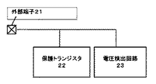
図2はテスト用動作モード検出機能を有した外部端子21、テスト用動作モード用電圧検出回路23、静電気的なノイズが印加した時にICを保護するための保護トランジスタ22を示したブロック図である。
【0008】
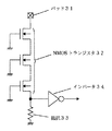
図3は一般的な従来の電圧検出回路を示す回路図である。テスト用動作モードに切り替えるために高電圧を印加するパッド31、n個のNMOSトランジスタ32、抵抗33、インバータ34から構成されている。パッド31とグランド電圧との間に直列にNMOSトランジスタ32と抵抗33が接続されており、抵抗33のハイ電圧側がインバータ34の入力となっている。この回路ではパッド31に直列接続されたn段分のNMOSトランジスタ32の閾値電圧の合計(n×Vth)よりも高い電圧が印加されるとインバータ34が反転し、出力はHレベルからLレベルに変化しテスト用動作モードに切り替わる。
【0009】
図2に示した保護トランジスタ22は、一般的にNMOSでありゲート電圧とソース電圧をグランド、ドレイン電圧をパッドに接続したオフトランジスタである。該保護トランジスタのMOS構造は電圧検出回路で用いたNMOSトランジスタよりもオフトランジスタのドレインブレークダウン耐圧が低いMOS構造のトランジスタを用いることによって、保護すべき内部トランジスタより先に保護トランジスタでブレークダウンし内部回路を保護する機能を有している。
【0010】
該保護トランジスタのドレイン電圧は、前述のとおり電圧検出回路のパッドに接続されたNMOSのドレインにも接続されている。
【0011】
このため保護トランジスタのドレインブレークダウン耐圧は、電圧検出回路の検出電圧よりも低い電圧に設定する必要がある。仮に検出電圧を保護トランジスタのドレインブレークダウン耐圧より高く設定した場合、該ブレークダウン耐圧以上の電圧を印加しても保護トランジスタでブレークダウンを起こし、ブレークダウン耐圧以上の電圧はかからないため電圧検出回路は検出することができず、それはすなわちテスト用動作モードに切り替えることができないことを示している。
【0012】
図4は、パッドに印加する電圧と電圧検出回路の直列に接続したNMOSトランジスタに流れる電流の関係を示したグラフである。
【0013】
パッドに電圧を印加する電圧を高くすると電圧に応じた電流が電圧検出回路に流れ、検出電圧(n×Vth)を印加すると前述のとおりテスト用動作モードに切り替わる。検出電圧より低い電圧では検出電流より少ない電流が電圧検出回路には流れる。
【0014】
通常動作モードの電源電圧範囲において、該電流は端子のリーク電流となり一般的に該リーク電流はEEPROMのIC仕様として一定電流値以下にする必要がある。特に低温時においてリーク電流は大きくなることから通常動作モードでの電源電圧範囲におけるリーク電流は製品として重要な要素となるものである。
【0015】
さらに検出電圧を高くすると最大動作電圧におけるリーク電流は少なくなり、検出電圧を低くすると最大動作電圧におけるリーク電流は多くなる。つまりリーク電流を少なくするためにはできる限り検出電圧を高く設定することが不可欠である。
【0016】
該電圧検出回路の設定可能な検出電圧の上限は、前記保護用オフトランジスタのドレインブレークダウン耐圧によって制限されるため該ドレインブレークダウン耐圧を高くする必要がある。
【0017】
しかし、該ドレインブレークダウン耐圧はMOSのゲート酸化膜厚やドレインの拡散濃度、フィールドの濃度をはじめとする半導体プロセスによって決定されるものであり、既に形成された半導体プロセスを使用する場合において容易にドレインブレークダウン耐圧のみを高くすることは不可能である。
【0018】
リーク電流が多くなる問題は、動作温度範囲が広く、特に低温で動作可能なICにおいて問題となる場合が多い。
【0019】
また、通常動作モードでの電源電圧範囲が広く、特に最大動作電圧の高いICにおいて問題になる場合が多い。
【0020】
また、保護トランジスタとして使用するオフトランジスタのドレインブレークダウン耐圧が低い場合、特に問題となる場合が多い。
【0021】
また、電圧検出回路を構成するNMOSトランジスタのサブスレッショルド電流が多い場合、特に問題になることが多い。
【0022】
【課題を解決するための手段】
そこで本発明は、上記問題を解決するために以下の手段を用いた。
本願発明にかかる半導体記憶装置は、テスト用動作モードに切り換える為の電圧が印加される外部端子と、前記外部端子と接地電位間に接続された保護トランジスタと、前記外部端子の電圧を検出し、テスト用動作モードに切り換える信号を出力する電圧検出回路と、を有し、前記保護トランジスタは、ドレイン領域がゲート電極で囲まれていることを特徴とする。
【0023】
さらに、前記電圧検出回路は、前記外部端子と接地電位の間に直列に接続された複数のMOSトランジスタを有し、前記直列に接続されたMOSトランジスタ間の接続点から前記信号を出力するものであり、前記外部端子に接続された前記MOSトランジスタは高耐圧MOSトランジスタであることを特徴とする。
【0024】
【本発明の実施の形態】
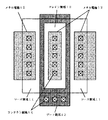
本発明の実施の形態を説明する。図1は、ドレインブレークダウン耐圧を高くすることを目的とした保護トランジスタの平面図である。
【0025】
図1に記したトランジスタは電気的にメタル電極12に接続されたゲート電極13により電気的に分離されたドレイン領域10とソース領域11にそれぞれコンタクト14を配置し、ドレイン領域10とソース領域11を、それぞれコンタクト14を介してメタル電極12に接続して所望の電気特性を得るものである。
【0026】
このトランジスタは外部端子に直接接続されているため、外部からのノイズが直接印加されノイズ耐性に優れた特性を有する。
【0027】
本発明ではドレイン領域10をゲート電極13で囲んだ構成とした。本構成を用いることによりドレイン領域10と素子分離領域との電気的な分離は、チャネル長方向端部のゲート電極13の電界効果を有するジャンクションダイオードで保たれているため、ノイズや静電気の電流経路の均一性が得られている。これによりドレインブレークダウン耐圧を向上させることができる。
【0028】
テスト用動作モードの切り替えを用とした電圧検出回路が備えられた外部端子の保護トランジスタに本発明によるトランジスタレイアウトを採用することにより、該電圧検出回路の検出電圧を高く設定することができ、延いては端子リーク電流を低減させた回路を実現することができるものである。
【0029】
本発明は、保護トランジスタのゲート領域となるレイアウトを変更する簡易な修正により、結果として端子リーク電流を容易な手段にて実現することが可能である。半導体プロセスのプロセスバイアスを一切変更することがなく目的を達成できる。
【0030】
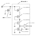
図5に、本発明を適用した実施例を示す。図5はテスト用動作モードに切り替えるための高電圧を印加する外部端子51、該外部端子51に接続した静電気的なノイズが印加した時ICを保護するための保護トランジスタ52、テスト用動作モードに切り替えるための高電圧を検出するための電圧検出回路53で構成している。
【0031】
電圧検出回路53は、外部端子にNMOSトランジスタ54のドレインが接続されており、該NMOSトランジスタ54のソースには飽和結線されたPMOSトランジスタ55が接続されており、該PMOSトランジスタ55のドレインにはPMOSトランジスタ56が接続されており、該PMOSトランジスタ56のゲート電圧はグランドである。該PMOSトランジスタ56のドレインはNMOSデプレッショントランジスタ57が接続され該NMOSデプレッショントランジスタ57のゲート電圧はグランドであり、一定電流59を流すことができる。PMOSトランジスタ56は、NMOSトランジスタ54とPMOSトランジスタ55とによって発生する電圧分がバックゲート電圧となりPMOSトランジスタ56の閾値電圧は高くなる。外部端子にバックゲート効果分を考慮したPMOSトランジスタ56の閾値以上の電圧を印加するとPMOSトランジスタ56にオン電流が流れる。該オン電流が前記一定電流59よりも大きくなると、インバータ58の出力はHレベルからLレベルに変化し、テスト用動作モードに切り替わる。
【0032】
NMOSトランジスタ54は高耐圧MOSで構成されており、該トランジスタのドレインジャンクションブレークダウン耐圧は一般的に20V程度と高い。
【0033】
前記保護トランジスタ52は低耐圧MOSで構成されており、一般的には該トランジスタのドレインジャンクションブレークダウン耐圧は12V程度である。本発明によるレイアウト構成を使用した保護トランジスタを用いることによりドレインジャンクションブレークダウン耐圧は1Vあるいは3V程度向上させることができる。
【0034】
【発明の効果】
以上、本願発明によれば、テスト動作モードでの端子リーク電流を低減した半導体記憶装置の提供が可能となる。
【図面の簡単な説明】
【図1】本発明の保護トランジスタ平面図を示す図である。
【図2】本発明の構成するブロック図を示す図である。
【図3】従来の電圧検出回路を示す図である。
【図4】電圧検出回路の特性グラフを示す図である。
【図5】本発明の実施の形態1の構成を示す図である。
【符号の説明】
11 ソース領域
12 メタル電極
13 ゲート領域
14 コンタクト領域[0001]
TECHNICAL FIELD OF THE INVENTION
The present invention relates to a semiconductor memory device, and more particularly, to an electrically rewritable nonvolatile semiconductor memory integrated circuit (hereinafter, referred to as an EEPROM). In addition, a test operation mode different from the normal operation mode is provided, and a circuit capable of switching to the test operation mode by applying a voltage higher than the voltage recommended in the normal operation mode to a predetermined external terminal is provided. The present invention relates to a semiconductor memory device.
[0002]
[Description of the Prior Art]
Some semiconductor memory devices have a function of switching to a test operation mode by applying a high voltage to an external terminal. The high voltage shown here indicates a voltage higher than the power supply voltage in the range applied in the normal operation mode. For example, if the maximum operation power supply voltage of the IC is 5 V, it indicates a voltage exceeding 5 V. Generally, a voltage of about 10 V is applied.
[0003]
In order to realize this function, a voltage detection circuit for detecting a high voltage is built in. In the above-described example, by setting the detection voltage of the voltage detection circuit to be more than 5 V and less than 10 V (generally 9 V), a voltage of 10 V is applied to a predetermined external terminal so that the voltage detection circuit detects the detection signal. Is output to switch to the test operation mode. Since the detection voltage is determined based on the specification of the maximum operating power supply voltage and the device characteristics of the semiconductor process to be used, it is conceivable that the voltage condition may be other than the above-described example.
[0004]
The external terminal to which a high voltage is applied is a dedicated terminal having the sole purpose of detecting the test operation mode and having no other function. In addition, the external terminal is a power supply voltage application terminal, and may be a terminal that has both a purpose of applying the power supply voltage and a voltage detection function for switching to a test operation mode. Further, the external terminal is an input terminal, an output terminal, or an input / output terminal, and may be a terminal that has both a function assigned to the terminal and a voltage detection function for switching to a test operation mode (for example, And
[0005]
[Patent Document 1]
Japanese Patent Application Laid-Open No. 2002-15599 (FIG. 2-4)
[0006]
[Problems to be solved by the invention]
The conventional voltage detection circuit for detecting the test operation mode has the following problems.
[0007]
FIG. 2 is a block diagram showing an external terminal 21 having a test operation mode detection function, a test operation mode voltage detection circuit 23, and a protection transistor 22 for protecting the IC when electrostatic noise is applied. .
[0008]
FIG. 3 is a circuit diagram showing a general conventional voltage detection circuit. It comprises a pad 31 for applying a high voltage to switch to the test operation mode, n NMOS transistors 32, a
[0009]
The protection transistor 22 shown in FIG. 2 is generally an NMOS, and is an off transistor in which a gate voltage and a source voltage are connected to ground, and a drain voltage is connected to a pad. The MOS structure of the protection transistor uses a MOS structure in which the drain breakdown voltage of the off transistor is lower than that of the NMOS transistor used in the voltage detection circuit. It has the function of protecting the circuit.
[0010]
The drain voltage of the protection transistor is also connected to the drain of the NMOS connected to the pad of the voltage detection circuit as described above.
[0011]
Therefore, it is necessary to set the drain breakdown voltage of the protection transistor to a voltage lower than the detection voltage of the voltage detection circuit. If the detection voltage is set higher than the drain breakdown voltage of the protection transistor, even if a voltage higher than the breakdown voltage is applied, a breakdown occurs in the protection transistor and a voltage higher than the breakdown voltage is not applied. No detection is possible, indicating that the test operating mode cannot be switched.
[0012]
FIG. 4 is a graph showing the relationship between the voltage applied to the pad and the current flowing through the NMOS transistor connected in series with the voltage detection circuit.
[0013]
When the voltage applied to the pad is increased, a current corresponding to the voltage flows to the voltage detection circuit, and when the detection voltage (n × Vth) is applied, the mode is switched to the test operation mode as described above. At a voltage lower than the detection voltage, a current smaller than the detection current flows through the voltage detection circuit.
[0014]
In the power supply voltage range in the normal operation mode, the current becomes a terminal leak current, and the leak current generally needs to be equal to or less than a certain current value according to the IC specification of the EEPROM. In particular, since the leak current increases at low temperatures, the leak current in the power supply voltage range in the normal operation mode is an important factor as a product.
[0015]
When the detection voltage is further increased, the leakage current at the maximum operating voltage decreases, and when the detection voltage is decreased, the leakage current at the maximum operation voltage increases. That is, in order to reduce the leak current, it is essential to set the detection voltage as high as possible.
[0016]
Since the upper limit of the detection voltage that can be set by the voltage detection circuit is limited by the drain breakdown voltage of the protection off transistor, it is necessary to increase the drain breakdown voltage.
[0017]
However, the drain breakdown voltage is determined by the semiconductor process including the gate oxide film thickness of the MOS, the diffusion concentration of the drain, and the concentration of the field. It is impossible to increase only the drain breakdown voltage.
[0018]
The problem that the leakage current increases is often a problem in an IC that can operate at a low temperature because of a wide operating temperature range.
[0019]
In addition, the power supply voltage range in the normal operation mode is wide, and this often causes a problem particularly in an IC having a high maximum operation voltage.
[0020]
Further, when the drain breakdown voltage of the off-transistor used as the protection transistor is low, it often causes a problem.
[0021]
Also, when the sub-threshold current of the NMOS transistor constituting the voltage detection circuit is large, it often causes a problem.
[0022]
[Means for Solving the Problems]
Therefore, the present invention uses the following means to solve the above problem.
A semiconductor memory device according to the present invention detects an external terminal to which a voltage for switching to a test operation mode is applied, a protection transistor connected between the external terminal and a ground potential, and a voltage of the external terminal, A voltage detection circuit that outputs a signal for switching to a test operation mode, wherein the protection transistor has a drain region surrounded by a gate electrode.
[0023]
Further, the voltage detection circuit has a plurality of MOS transistors connected in series between the external terminal and a ground potential, and outputs the signal from a connection point between the MOS transistors connected in series. The MOS transistor connected to the external terminal is a high voltage MOS transistor.
[0024]
[Embodiment of the present invention]
An embodiment of the present invention will be described. FIG. 1 is a plan view of a protection transistor for the purpose of increasing the drain breakdown voltage.
[0025]
In the transistor shown in FIG. 1, contacts 14 are respectively arranged in a drain region 10 and a source region 11 which are electrically separated by a
[0026]
Since this transistor is directly connected to an external terminal, external noise is directly applied to the transistor, and the transistor has excellent noise resistance.
[0027]
In the present invention, the drain region 10 is surrounded by the
[0028]
By employing the transistor layout according to the present invention for the protection transistor of the external terminal provided with the voltage detection circuit for switching the test operation mode, the detection voltage of the voltage detection circuit can be set high, and the In addition, a circuit with reduced terminal leak current can be realized.
[0029]
According to the present invention, it is possible to realize a terminal leak current by a simple means as a result of a simple modification for changing a layout serving as a gate region of a protection transistor. The object can be achieved without changing the process bias of the semiconductor process at all.
[0030]
FIG. 5 shows an embodiment to which the present invention is applied. FIG. 5 shows an external terminal 51 for applying a high voltage for switching to a test operation mode, a protection transistor 52 for protecting the IC when electrostatic noise is applied to the external terminal 51, and a test operation mode. It comprises a voltage detection circuit 53 for detecting a high voltage for switching.
[0031]
The voltage detection circuit 53 has an external terminal connected to the drain of the NMOS transistor 54, a source connected to the PMOS transistor 55 connected in saturation, and a drain connected to the PMOS transistor 55. The transistor 56 is connected, and the gate voltage of the PMOS transistor 56 is ground. The drain of the PMOS transistor 56 is connected to the NMOS depletion transistor 57, and the gate voltage of the NMOS depletion transistor 57 is ground, so that a constant current 59 can flow. In the PMOS transistor 56, the voltage generated by the NMOS transistor 54 and the PMOS transistor 55 becomes the back gate voltage, and the threshold voltage of the PMOS transistor 56 increases. When a voltage higher than the threshold value of the PMOS transistor 56 in consideration of the back gate effect is applied to the external terminal, an ON current flows through the PMOS transistor 56. When the on-current becomes larger than the constant current 59, the output of the inverter 58 changes from the H level to the L level, and switches to the test operation mode.
[0032]
The NMOS transistor 54 is composed of a high withstand voltage MOS, and the drain junction breakdown voltage of the transistor is generally as high as about 20V.
[0033]
The protection transistor 52 is formed of a low withstand voltage MOS, and generally has a drain junction breakdown withstand voltage of about 12V. By using the protection transistor using the layout configuration according to the present invention, the drain junction breakdown voltage can be improved by about 1 V or 3 V.
[0034]
【The invention's effect】
As described above, according to the present invention, it is possible to provide a semiconductor memory device with reduced terminal leak current in the test operation mode.
[Brief description of the drawings]
FIG. 1 is a plan view showing a protection transistor according to the present invention.
FIG. 2 is a diagram showing a block diagram constituting the present invention.
FIG. 3 is a diagram illustrating a conventional voltage detection circuit.
FIG. 4 is a diagram showing a characteristic graph of the voltage detection circuit.
FIG. 5 is a diagram showing a configuration of the first embodiment of the present invention.
[Explanation of symbols]
11
Claims (2)
前記外部端子と接地電位間に接続された保護トランジスタと、
前記外部端子の電圧を検出し、所定の電圧以上であれば第1の動作モードから第2の動作モードに切り換える信号を出力する電圧検出回路と、を有し、
前記保護トランジスタは、ドレイン領域がゲート電極で囲まれていることを特徴とする半導体記憶装置。An external terminal to which a voltage for switching the operation mode is applied,
A protection transistor connected between the external terminal and a ground potential;
A voltage detection circuit that detects a voltage of the external terminal and outputs a signal for switching from the first operation mode to the second operation mode if the voltage is equal to or higher than a predetermined voltage,
A semiconductor memory device, wherein the protection transistor has a drain region surrounded by a gate electrode.
前記直列に接続されたMOSトランジスタ間の接続点から前記信号を出力するものであり、前記外部端子に接続された前記MOSトランジスタは高耐圧MOSトランジスタであることを特徴とする請求項1に記載の半導体記憶装置。The voltage detection circuit has a plurality of MOS transistors connected in series between the external terminal and a ground potential,
2. The MOS transistor according to claim 1, wherein the signal is output from a connection point between the MOS transistors connected in series, and the MOS transistor connected to the external terminal is a high voltage MOS transistor. Semiconductor storage device.
Priority Applications (3)
| Application Number | Priority Date | Filing Date | Title |
|---|---|---|---|
| JP2003013801A JP2004228317A (en) | 2003-01-22 | 2003-01-22 | Semiconductor memory device |
| US10/761,954 US6980475B2 (en) | 2003-01-22 | 2004-01-21 | Semiconductor memory device |
| CNB2004100059035A CN100538911C (en) | 2003-01-22 | 2004-01-21 | Semiconductor storage unit |
Applications Claiming Priority (1)
| Application Number | Priority Date | Filing Date | Title |
|---|---|---|---|
| JP2003013801A JP2004228317A (en) | 2003-01-22 | 2003-01-22 | Semiconductor memory device |
Publications (1)
| Publication Number | Publication Date |
|---|---|
| JP2004228317A true JP2004228317A (en) | 2004-08-12 |
Family
ID=32866192
Family Applications (1)
| Application Number | Title | Priority Date | Filing Date |
|---|---|---|---|
| JP2003013801A Withdrawn JP2004228317A (en) | 2003-01-22 | 2003-01-22 | Semiconductor memory device |
Country Status (3)
| Country | Link |
|---|---|
| US (1) | US6980475B2 (en) |
| JP (1) | JP2004228317A (en) |
| CN (1) | CN100538911C (en) |
Cited By (2)
| Publication number | Priority date | Publication date | Assignee | Title |
|---|---|---|---|---|
| JP2009210448A (en) * | 2008-03-05 | 2009-09-17 | Toshiba Corp | Semiconductor device |
| CN101930982A (en) * | 2010-07-07 | 2010-12-29 | 中国电子科技集团公司第五十八研究所 | FLOTOX structure-based anti-radiation EEPROM storage unit structure |
Families Citing this family (5)
| Publication number | Priority date | Publication date | Assignee | Title |
|---|---|---|---|---|
| JP2009141278A (en) * | 2007-12-10 | 2009-06-25 | Toshiba Corp | Nonvolatile semiconductor memory device |
| KR102124628B1 (en) * | 2013-05-16 | 2020-06-19 | 삼성전자주식회사 | Test structures of semiconductor device |
| US9082739B2 (en) | 2013-05-16 | 2015-07-14 | Samsung Electronics Co., Ltd. | Semiconductor device having test structure |
| JP2019054102A (en) * | 2017-09-14 | 2019-04-04 | 東芝メモリ株式会社 | Storage device and manufacturing method thereof |
| CN110364522B (en) * | 2018-03-26 | 2021-10-08 | 瑞昱半导体股份有限公司 | Circuit Architecture to Protect Low Voltage Components |
Family Cites Families (5)
| Publication number | Priority date | Publication date | Assignee | Title |
|---|---|---|---|---|
| JPS55149871A (en) * | 1978-07-31 | 1980-11-21 | Fujitsu Ltd | Line voltage detector |
| KR100272164B1 (en) * | 1997-12-30 | 2000-11-15 | 윤종용 | Semiconductor device having mode register set circuit |
| US6081466A (en) * | 1998-10-30 | 2000-06-27 | Stmicroelectronics, Inc. | Stress test mode entry at power up for low/zero power memories |
| JP2002033000A (en) * | 2000-07-14 | 2002-01-31 | Mitsubishi Electric Corp | Semiconductor storage device |
| JP4257486B2 (en) * | 2002-02-14 | 2009-04-22 | Okiセミコンダクタ株式会社 | DRAM power supply control device |
-
2003
- 2003-01-22 JP JP2003013801A patent/JP2004228317A/en not_active Withdrawn
-
2004
- 2004-01-21 CN CNB2004100059035A patent/CN100538911C/en not_active Expired - Fee Related
- 2004-01-21 US US10/761,954 patent/US6980475B2/en not_active Expired - Lifetime
Cited By (2)
| Publication number | Priority date | Publication date | Assignee | Title |
|---|---|---|---|---|
| JP2009210448A (en) * | 2008-03-05 | 2009-09-17 | Toshiba Corp | Semiconductor device |
| CN101930982A (en) * | 2010-07-07 | 2010-12-29 | 中国电子科技集团公司第五十八研究所 | FLOTOX structure-based anti-radiation EEPROM storage unit structure |
Also Published As
| Publication number | Publication date |
|---|---|
| US20040165451A1 (en) | 2004-08-26 |
| US6980475B2 (en) | 2005-12-27 |
| CN1542859A (en) | 2004-11-03 |
| CN100538911C (en) | 2009-09-09 |
Similar Documents
| Publication | Publication Date | Title |
|---|---|---|
| US6573566B2 (en) | Low-voltage-triggered SOI-SCR device and associated ESD protection circuit | |
| JP4402109B2 (en) | Low voltage NMOS type electrostatic discharge clamp | |
| US5341003A (en) | MOS semiconductor device having a main unit element and a sense unit element for monitoring the current in the main unit element | |
| JP3639596B2 (en) | Protective switch | |
| US5760630A (en) | Input protection circuit having load resistor implemented by p-channel MIS transistor | |
| JP3164065B2 (en) | Semiconductor device | |
| US20080246345A1 (en) | Semiconductor Switch Arrangement and an Electronic Device | |
| US6469352B2 (en) | Two-terminal semiconductor overcurrent limiter | |
| US20130076400A1 (en) | Comparator circuit | |
| US6778366B2 (en) | Current limiting protection circuit | |
| US6088208A (en) | Electronic device, electronic switching apparatus including the same, and production method thereof | |
| US7733133B2 (en) | Power switch circuit having variable resistor coupled between input terminal and output transistor and changing its resistance based on state of output transistor | |
| US20030043517A1 (en) | Electro-static discharge protecting circuit | |
| JP2004228317A (en) | Semiconductor memory device | |
| CN110085583B (en) | Semiconductor device and operating method | |
| US9293451B2 (en) | Integrated circuit electrical protection device | |
| CN101236965B (en) | Semiconductor integrated circuit device | |
| JP3431127B2 (en) | Electronic device and electronic switch device | |
| US7723794B2 (en) | Load driving device | |
| US20250015075A1 (en) | Semiconductor apparatus | |
| JP3544499B2 (en) | Semiconductor integrated circuit device | |
| JP2007095848A (en) | Semiconductor device | |
| US20090302397A1 (en) | Field-Effect Transistor | |
| JP2003338555A (en) | Electronic switch device and manufacturing method thereof | |
| JP3187773B2 (en) | Semiconductor device with input protection element |
Legal Events
| Date | Code | Title | Description |
|---|---|---|---|
| A621 | Written request for application examination |
Free format text: JAPANESE INTERMEDIATE CODE: A621 Effective date: 20050809 |
|
| A977 | Report on retrieval |
Free format text: JAPANESE INTERMEDIATE CODE: A971007 Effective date: 20080313 |
|
| A131 | Notification of reasons for refusal |
Free format text: JAPANESE INTERMEDIATE CODE: A131 Effective date: 20090324 |
|
| A761 | Written withdrawal of application |
Free format text: JAPANESE INTERMEDIATE CODE: A761 Effective date: 20090512 |