JP2004227940A - Display body, display panel, display device, and manufacturing method - Google Patents
Display body, display panel, display device, and manufacturing method Download PDFInfo
- Publication number
- JP2004227940A JP2004227940A JP2003014730A JP2003014730A JP2004227940A JP 2004227940 A JP2004227940 A JP 2004227940A JP 2003014730 A JP2003014730 A JP 2003014730A JP 2003014730 A JP2003014730 A JP 2003014730A JP 2004227940 A JP2004227940 A JP 2004227940A
- Authority
- JP
- Japan
- Prior art keywords
- light
- emitting element
- light emitting
- display panel
- microlens
- Prior art date
- Legal status (The legal status is an assumption and is not a legal conclusion. Google has not performed a legal analysis and makes no representation as to the accuracy of the status listed.)
- Withdrawn
Links
- 238000004519 manufacturing process Methods 0.000 title claims description 14
- 238000000034 method Methods 0.000 claims abstract description 25
- 239000011347 resin Substances 0.000 claims description 17
- 229920005989 resin Polymers 0.000 claims description 17
- 238000007599 discharging Methods 0.000 claims description 12
- 230000003287 optical effect Effects 0.000 claims description 9
- 239000011261 inert gas Substances 0.000 claims description 7
- 239000011159 matrix material Substances 0.000 claims description 6
- 239000000758 substrate Substances 0.000 claims description 3
- 230000000694 effects Effects 0.000 description 4
- 238000005516 engineering process Methods 0.000 description 3
- XKRFYHLGVUSROY-UHFFFAOYSA-N Argon Chemical compound [Ar] XKRFYHLGVUSROY-UHFFFAOYSA-N 0.000 description 2
- 238000010586 diagram Methods 0.000 description 2
- 239000007789 gas Substances 0.000 description 2
- 239000000463 material Substances 0.000 description 2
- 230000003647 oxidation Effects 0.000 description 2
- 238000007254 oxidation reaction Methods 0.000 description 2
- IJGRMHOSHXDMSA-UHFFFAOYSA-N Atomic nitrogen Chemical compound N#N IJGRMHOSHXDMSA-UHFFFAOYSA-N 0.000 description 1
- 238000010521 absorption reaction Methods 0.000 description 1
- 229910052786 argon Inorganic materials 0.000 description 1
- 239000006059 cover glass Substances 0.000 description 1
- 230000002542 deteriorative effect Effects 0.000 description 1
- 229910001873 dinitrogen Inorganic materials 0.000 description 1
- 238000005401 electroluminescence Methods 0.000 description 1
- 238000000605 extraction Methods 0.000 description 1
- 238000010030 laminating Methods 0.000 description 1
- 238000007789 sealing Methods 0.000 description 1
- 230000009747 swallowing Effects 0.000 description 1
Images


Classifications
-
- H—ELECTRICITY
- H10—SEMICONDUCTOR DEVICES; ELECTRIC SOLID-STATE DEVICES NOT OTHERWISE PROVIDED FOR
- H10K—ORGANIC ELECTRIC SOLID-STATE DEVICES
- H10K59/00—Integrated devices, or assemblies of multiple devices, comprising at least one organic light-emitting element covered by group H10K50/00
- H10K59/80—Constructional details
- H10K59/875—Arrangements for extracting light from the devices
- H10K59/879—Arrangements for extracting light from the devices comprising refractive means, e.g. lenses
Landscapes
- Electroluminescent Light Sources (AREA)
Abstract
Description
【0001】
【発明の属する技術分野】
本発明は、有機エレクトロルミネセンス(有機EL)等の発光素子を有する表示体および表示パネルに関するものである。
【0002】
【従来の技術】
特開2001−135477号公報の図11には、透明板の積層側が平面であり、積層側と反対側である観測側は凸状のレンズであり、各絵素毎に1ケの片面凸レンズを形成した有機EL素子が開示されている。絵素単位で考えると、発光色材から臨界角以上で出力された光も凸レンズの部分では臨界角以下となり、観測側に届くことができるので取り出し効率が向上する。
【0003】
【特許文献1】
特開2001−135477号公報
【0004】
【発明が解決しようとする課題】
無機や有機のELを用いた上記の表示パネルのような自発光型の表示パネルにおいては、光の利用効率の向上、明るさの向上および消費電力の低減が常に求められる課題である。従来の自発光表示パネルは、屈折率が1より大きな透明媒質中で発光素子が発光し、その発光面を透明媒質の表面と空気との界面を通して見るものである。発光面からは、光がほぼすべての角度に発射されるために、その光の一部は、透明媒質の表面と空気との界面に対して全反射角以上で入射し、透明媒質から空気あるいは外界に出ることができず、光の利用効率を向上できない大きな要因となっている。上述した凸レンズを透明媒質の界面に配置した表示パネルは、光の利用効率を高められる点で優れている。しかしながら、発光面からレンズまでの間に厚みがあり、その間を通って発散した光まで外界に出力させるようなレンズ設計を行なうと、隣接する画素とのクロストークが問題になる。したがって、レンズの曲率を大きくすることはできず、レンズへの光の飲み込み量が少ないので、臨界角以上で出力された光の多くを利用できるようにすることは不可能である。
【0005】
そこで、本発明においては、発光素子の前面にマイクロレンズを配置した表示体および表示パネルにおいてレンズの飲み込み量を向上することができる表示体および表示パネルを提供することを目的としている。そして、光の利用効率をさらに向上できる表示体および表示パネルを提供することを目的としている。
【0006】
【課題を解決するための手段】
上述したクロストークの問題を解決するためには、発光素子から放出された光が、隣接する画素を形成するレンズに到達しないようにすればよく、たとえば、画素間にマイクロミラーを形成して分離することができる。しかしながら、マイクロミラーを形成する工程が増え、マイクロミラーをアレンジする厚みが必要になるために表示体および表示パネルが厚くなる。したがって、経済的な解ではなく、また、製品上も好ましい解であるとは言えない。そこで、本発明においては、発光素子の上の少なくとも発光素子の1辺の長さ以内の位置にレンズを配置し、隣接する画素へ光が伝播される空間を縮小する。これにより、クロストークの発生を防止できると共に、発光素子から放出される光のさらに多くをレンズに飲み込ませることが可能となり、観測側あるいは外界に出力することができる。したがって、光の利用効率を大幅に向上できる。すなわち、本発明の表示体は、電極間に発光素子が配置され、電極間に印加される電圧により発光素子が発光する発光層と、発光素子からの光が出力される射出方向の電極の上の少なくとも発光素子の1辺の長さ以内の位置に、少なくとも1つのマイクロレンズが形成されたレンズ層とを有する。
【0007】
したがって、複数の本発明の表示体を2次元にマトリクス状に配置した表示パネルにより、さらにコントラストが高く、鮮明なカラー画像が表示可能な表示パネルを提供できる。また、本発明の表示パネルと、この表示パネルの発光素子を駆動して画像を表示させる駆動装置とを有する表示装置により鮮明な画像を表示できる表示装置を提供できる。
【0008】
この表示体あるいは表示パネルにおいては、電極の上の少なくとも発光素子の1辺の長さ以内の位置にマイクロレンズが配置され、隣接するレンズに光が伝達される媒体あるいは媒質の厚みを限定し、クロストークを少なくして輝度と鮮度を向上させようとするものである。特に、電極の直上にマイクロレンズを配置することにより、隣接する画素へ光が伝播される空間を無くすあるいは最小限にすることができる。そして、隣接するレンズに光が伝達される媒体あるいは媒質の厚みを無くすことにより、個々のレンズ、あるいは少なくとも発光素子あるいは画素単位のレンズが独立した形状となる。したがって、マイクロレンズアレイあるいはマイクロレンズアレイシートを形成することができず、自発光素子を用いた表示パネルをシート材を積層する方法では製造できない。しかしながら、近年、プリンタに採用されているインクジェット技術はμmオーダの微細なドットを形成することが可能である。したがって、インクジェット方式でマイクロレンズを形成すれば、μmのオーダの形状および位置精度で独立したマイクロレンズを形成することが可能であり、本発明の表示体および表示パネルを実際に製造することができる。
【0009】
すなわち、本発明の表示体の製造方法は、電極間に発光素子が配置され、電極間に印加される電圧により発光素子が発光する発光層の、発光素子からの光が出力される射出方向の電極の上の少なくとも発光素子の1辺の長さ以内の位置に、微小液滴吐出装置により透明樹脂を吐出し、集光用のマイクロレンズを形成するマイクロレンズ形成工程を有する。また、本発明の表示パネルの製造方法は、電極間に発光素子が配置され、電極間に印加される電圧により発光素子が発光する発光層であって、複数の発光素子が2次元にマトリクス状に配置された発光層の、発光素子からの光が出力される射出方向の電極の上の少なくとも発光素子の1辺の長さ以内の位置に、微小液滴吐出装置により透明樹脂を吐出し、複数の集光用のマイクロレンズを形成するマイクロレンズ形成工程を有する。微小液滴吐出装置として最適なものはインクジェット方式で透明樹脂を吐出する装置であり、そのような微小液滴吐出装置は、すでに技術が確立しているプリンタ用のインク吐出装置を流用することができる。そして、このインクジェット方式であれば、発光素子の電極の直ぐ上に、独立した形状で隣接するマイクロレンズに光が伝達される空間が殆どない状態のマイクロレンズを形成できる。
【0010】
インクジェット方式によりマイクロレンズを形成する方法は、他の光学装置の製造方法にも適用できるものである。すなわち、光学素子が2次元に配置された光学素子層の射出側に、微小液滴吐出装置により透明樹脂を吐出し、複数の集光用のマイクロレンズを形成するマイクロレンズ形成工程を有する光学装置の製造方法も本発明に含められる。
【0011】
インクジェット方式によりマイクロレンズを形成することにより、凸レンズまたは半球レンズを形成でき、複数のマイクロレンズを形成したときに各々のマイクロレンズがほぼ独立した形状にすることができる。したがって、隣接する発光素子からの光がマイクロレンズ内に侵入することがほとんどないので、マイクロレンズの曲率を十分に大きくすることができ、発光素子から前方に放散されるほとんどの光をレンズに飲み込ませて外界に出力できる。
【0012】
このマイクロレンズで発光素子を機械的にカバーすることも可能であり、マイクロレンズの径を発光素子の径(方形の発光素子であれば対角線の長さ)よりも大きくすることで隙間なく発光素子をカバーできる。一方、発光素子の上の少なくとも発光素子の1辺の長さ以内の位置に複数のさらに小さなマイクロレンズを配置することも可能であり、その場合は、マイクロレンズ間に隙間が生ずる可能性があるので、電極の幅を発光素子の幅より広げて、電極により発光素子をカバーすることが望ましい。
【0013】
さらに、本発明にかかる表示パネルにおいては、発光素子から放散された光のほとんどが凸状のマイクロレンズに飲み込まれ、角度が射出方向にほぼ整った状態で出力される。したがって、レンズ層の射出方向に透明なカバー層を配置しても、カバー層の界面に対して臨界角以上で入射される光はほとんどなくなり、光の利用効率を低下させずに透明カバーを取り付けることができる。さらに、カバー層とレンズ層との間に屈折率がほぼ1である不活性ガスを充填することにより、レンズ層を保護でき、また、レンズとその周囲との屈折率差が十分になるので、十分なレンズ効果を得ることができる。
【0014】
【発明の実施の形態】
以下に図面を参照して本発明をさらに詳しく説明する。図1に示した携帯電話機1は、本発明に係る表示パネルを備えた表示装置を有する。携帯電話機1においてデータが表示される表示パネル3は、自発光型の素子である有機ELがマトリクス状に配置された発光層4と、その発光層4から発する光8をユーザ9がみやすい所望の方向に集光するレンズ層5と、カバーガラス6とを備えている。この表示パネル3は、マイクロコンピュータなどから構成される駆動装置2により、発光層4の有機ELが画素単位で発光され、それらから出力された光8によって、文字や画像などのデータがユーザ9に表示できる。
【0015】
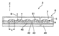
図2に、表示パネル3の概略構成を示してある。図2は、表示パネル3を部分的に拡大した断面図である。本例の発光層4は、上下の電極42および43の間に1辺の長さがxの発光素子45である有機ELが配置された構成となっており、電極42および43の間に印加される電圧により発光素子45が発光する。そして、発光層4の背面側には、基板を兼ねて光を吸収する吸収層49が設けられており、外光や発光素子45から背面に放出された光を吸収し前方(射出方向)Zにおけるコントラストが低下しないようにしている。
【0016】
レンズ層5は、発光素子45からの光8が出力される射出方向Zの電極42の上の発光素子45の1辺の長さx以内であって、光8の飲み込み量が最も高くなる位置、すなわち、電極42の直上に形成された複数のマイクロレンズ51を備えている。さらに、レンズ層5の射出方向Zに透明なカバー層6が配置されており、カバー層6とレンズ層5との間に屈折率がほぼ1である不活性ガス7が充填されている。
【0017】
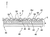
図3に、発光層4と、レンズ層5とをさらに拡大して示してある。各々の発光素子45の直上に透明電極42を挟んで凸状のマイクロレンズ51が形成されている。したがって、1つの発光素子45を備えた表示体46としてみると、各々の表示体46が1つのマイクロレンズ51を備えており、複数の表示体46が2次元方向にマトリクス状に配置されて表示パネル3を構成している。有機ELは密封する必要があるが、本例の表示パネル3においては、各々発光素子45は、透明電極42とマイクロレンズ51とで封止された状態で表示パネル3が形成されている。
【0018】
透明電極42の直上に形成された各々のマイクロレンズ51は、独立しており、ある発光素子45から放出された光8は、その発光素子45に対応するマイクロレンズ51に飲み込まれ、隣接する発光素子45に対応する他のマイクロレンズ51に伝達されることはほぼない。したがって、本例の表示パネル3においては、発光素子45から広い角度で放散される光8のほとんどをマイクロレンズ51により射出方向Zに向きを変えて外部に出力できる。特に、広い角度で出力された発散光8wは、レンズ層5が平面的な層であれば、外界との界面における臨界角以上の角度の光となり、外界には出力されない。しかしながら、レンズ層5を採用することにより、臨界角以下でレンズ51の界面52に入射させることが可能となり、外界に発散光8wを出力することができる。このため、本例の表示パネル3においては、発光素子45から出力される光8の利用効率を向上でき、明るく鮮明な画像を表示するのに適している。
【0019】
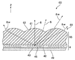
図4に、複数のマイクロレンズ61がシート69に形成された状態で発光層4に積層された表示パネル60を示してある。このような表示パネル60であると、発光素子45からマイクロレンズ61の屈折面あるいは界面62までの距離が長く、さらに複数のマイクロレンズ61をシート状にするために複数のマイクロレンズ61に共通する、あるいは支持する透明媒体部65がある。したがって、ある発光素子45から出力された光のうち、放出角度の大きな発散光8wは、隣接する発光素子45に対応するマイクロレンズ61の界面62に到達する可能性がある。このような発散光8wまでマイクロレンズ61から外界に放出されると、発光素子45の間でクロストークが発生し、コントラストが低下すると共に画質が劣化する。したがって、マイクロレンズ61の界面62は、入射角度の大きな発散光8wは外界に出ないような曲率となるように設計せざるを得ない。このため、マイクロレンズを発光素子45の前面に配置しても、それほど光の利用効率は向上しない。
【0020】
これに対し、図3に示した本発明にかかる表示パネル3においては、複数のマイクロレンズ51が独立した形状で成形されているので、隣接する発光素子45からの光はマイクロレンズ51に伝達されない。したがって、マイクロレンズ51の界面52の曲率は自由に設計することが可能であり、発光素子45から大きな角度で出力される発散光8wも含めて外界に出力できるような曲率のマイクロレンズとすることができる。
【0021】
図5に、本発明の異なる表示パネル31の発光層4およびレンズ層5の組み合わせを拡大して示してある。上述した凸レンズ状のマイクロレンズ51は曲率が小さいので比較的作成が容易であり、さらに、発光素子45に一対一で対応したサイズとなっているので、その点でも作成が容易である。一方、本発明にかかる表示パネルにおいては、マイクロレンズの界面の曲率は自由に選択することができ、本例の表示パネル31においては、ほぼ半球状の界面54を備えた独立したマイクロレンズ53を、各々の発光素子45に対応して設けている。曲率半径が小さく、曲率の大きな半球状のマイクロレンズ53を採用することにより、発散光8wをさらに効率良く外界に出力することができ、また、外界に出力された光の方向を射出方向Zに揃えやすい。したがって、このレンズ層5の前面に透明なカバー層6が配置されている場合であっても、透明なカバー層6を透過する光をさらに多くすることができ、さらに明るい画像を表示できる。
【0022】
図6に、本発明のさらに異なる表示パネル32を示してある。また、図7に、表示パネル32の発光層4およびレンズ層5を抜き出してさらに拡大して示してある。本例の表示パネル32においては、1つの発光素子45に対応して複数のマイクロレンズ55が設けられている。個々のマイクロレンズ55は独立しており、透明電極42の直上に配置されている。このため、上述した表示パネル3および31と同様に、レンズ55に起因してクロストークが発生する可能性はほとんどなく、レンズ55の界面56を自由に設計できる。そして、本例においては、レンズ55の界面56はほぼ半球状であり、上述した表示パネル31と同様に広い範囲の発散光8wを外界に出力でき、さらに、出力された光の方向を射出方向Zに揃えやすい表示パネルである。さらに、1つの発光素子45に対応して複数のマイクロレンズ55を配置することにより、個々のマイクロレンズ55は小さくなり高さも低くなる。したがって、光の利用効率が高く、さらに、非常に薄い表示パネル32を提供することが可能となる。
【0023】
一方、1つの発光素子45に対応して、その上を複数のマイクロレンズ55で覆うことにより、マイクロレンズ55の間に隙間が発生しやすくなる。しかしながら、本例の表示パネル32においては、射出側の電極42の幅を発光素子45の幅に対して十分に広くすることにより、透明電極42により発光素子45を密封することができる。したがって、上記の表示パネル3および31においては、マイクロレンズ51または53がEL製の発光素子45を密封する機能を発揮していたが、本例のようなさらに小さな複数のマイクロレンズ51を配置する場合であっても透明電極42で十分に発光素子45は密封できる。このため、本発明の表示パネルは、有機ELを発光素子として採用した表示パネルにおいて十分に対応できる。また、機械的な強度は、透明電極42に重ねてマイクロレンズ55を配置することにより十分に確保できる。
【0024】
1つの発光素子45に対応して複数のマイクロレンズ55を配置する本例の表示パネル32においては、1つ1つのマイクロレンズ55のサイズは小さくなる。しかしながら、発光素子45の大きさが10μmのオーダであると、マイクロレンズ55の形状および配置精度のオーダは1μmから10μmのオーダであり、現状のインクジェット技術により十分に対応できる。さらに、各々のマイクロレンズ55が個々の発光素子45に対応している必要はないので、アライメントフリーになりその点では製造しやすい表示パネルとなる。
【0025】
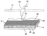
図8に、複数の発光素子45が2次元にマトリクス状に配置された発光層4の射出方向の電極42の直上に、微小液滴吐出装置であるインクジェットヘッド70により樹脂滴72を吐出し、マイクロレンズ55を形成する過程を示してある。インクジェットヘッド70はプリンタと同様にキャリッジシャフト71を往復動しながら供給パイプ75から供給された屈折率が約1.5の樹脂を適切な量だけ吐出し、所望の位置に所望の大きさのマイクロレンズを形成する。個々のマイクロレンズの形状は吐出量や吐出する樹脂の粘度などを調整することにより自由に設定できる。
【0026】
発光層4の上に、マイクロレンズ55からなるレンズ層5が形成された基板49に、図6に示すように、マイクロレンズ55の半径よりも深い段差を有する段差付き透明部材6がカバー層として装着される。カバー層6の取り付けを不活性ガス7の雰囲気で行なうことにより、カバー層6の内部を不活性ガス7で満たすことができる。カバー層6の内部は空気で満たしても良いが、空気中の水分によるELの劣化を確実に防止すること、また、マイクロレンズ55を形成する樹脂が酸化などにより劣化する可能性があることを考慮すると窒素ガスあるいはアルゴンガスなどの不活性ガス7を採用することが好ましい。
【0027】
さらに、樹脂の酸化や表示パネルの強度を考慮すると、カバー層6の内部を適当な透明の樹脂で満たすことも可能である。しかしながら、樹脂の屈折率はガスあるいは空気よりも大きく、多くの樹脂の屈折率は1よりも大きい。したがって、マイクロレンズ55との屈折率の差が小さくなってしまい、マイクロレンズ55のレンズ効果が薄れ、外界に出力された光8を射出方向Zに揃えにくくなる。カバー層6で覆った場合、カバー層6の表面6sが再度、外界に対する界面となるので、その界面6sで臨界角が生じ、臨界角以上で入射された光はカバー層6から外界に出力されなくなる。したがって、マイクロレンズ55から出力される光はできる限り射出方向Zに向いていることが望ましく、そのためにはマイクロレンズ55の屈折力は高いことが望ましい。
【0028】
図8には、1つの発光素子45に複数のマイクロレンズ55が配置された表示パネル32を例にインクジェット方式を用いた製造方法を示しているが、図3および図5に示した表示パネル3および31も同様にインクジェット方式でマイクロレンズ51および53を形成することができる。そして、上記と同様のプロセスで内部に不活性ガス7が封入された状態でカバー6を取付けることができ、耐久性があり、さらに、光の利用効率の高い表示パネルを提供することができる。
【0029】
なお、本発明の実施の形態では、光8が出力される射出方向Zの電極42の直ぐ上にマイクロレンズ51、53または55を配置しているが、マイクロレンズを配置する位置はこれに限定されるのもではなく、光8が出力される射出方向Zの電極42の上の少なくとも発光素子45の1辺の長さx以内の位置であれば、同様の効果を得ることが可能である。
【0030】
また、本発明にかかる表示パネル3、31および32は、上述した携帯電話機1にかぎらず、カーナビゲーションシステム、コンピュータのモニタ、テレビなどのあらゆる分野の表示装置に適用可能であり、明るく、鮮明な画像が表示可能で消費電力が小さな表示装置を提供できる。
【0031】
【発明の効果】
以上説明したように、本発明においては、インクジェット方式などの微小液滴吐出装置を用い、独立したマイクロレンズを、発光素子の電極の上の少なくとも発光素子の1辺の長さ以内の位置、特に、電極の直ぐ上に形成するようにしている。これにより、発光素子から出力された光がマイクロレンズに飲み込まれて外界に出力される量を大きくできるので、光の利用効率が高く、明るい画像を表示可能な表示パネルを提供することができる。
【図面の簡単な説明】
【図1】本発明に係る表示パネルが搭載された表示装置を備えた携帯電話機を示す図である。
【図2】本発明に係る表示パネルの概略構成を示す断面図である。
【図3】図2に示す表示パネルの発光層およびレンズ層をさらに拡大して示す断面図である。
【図4】図3に示す表示パネルと対比するために連続したマイクロレンズを備えた表示パネルを示す図である。
【図5】図3と異なる表示パネルの発光層およびレンズ層を示す断面図である。
【図6】さらに異なる表示パネルの概略構成を示す断面図である。
【図7】図6に示す表示パネルの発光層およびレンズ層を示す断面図である。
【図8】図6に示す表示パネルの製造過程を示す図である。
【符号の説明】
1 携帯電話機
2 駆動装置
3、31、32 表示パネル
4 発光層
5 レンズ層
51、53、55 マイクロレンズ[0001]
TECHNICAL FIELD OF THE INVENTION
The present invention relates to a display and a display panel having a light emitting element such as an organic electroluminescence (organic EL).
[0002]
[Prior art]
In FIG. 11 of JP-A-2001-135377, the laminated side of the transparent plate is a plane, and the observation side opposite to the laminated side is a convex lens. One single-sided convex lens is provided for each picture element. The formed organic EL device is disclosed. In terms of picture elements, light output from the luminescent color material at a critical angle or more is also less than the critical angle at the convex lens portion and can reach the observation side, so that the extraction efficiency is improved.
[0003]
[Patent Document 1]
Japanese Patent Application Laid-Open No. 2001-135377
[Problems to be solved by the invention]
In a self-luminous display panel such as the above-described display panel using an inorganic or organic EL, it is a problem that the improvement of light use efficiency, the improvement of brightness, and the reduction of power consumption are always required. In a conventional self-luminous display panel, a light-emitting element emits light in a transparent medium having a refractive index greater than 1, and its light-emitting surface is viewed through an interface between the surface of the transparent medium and air. Since light is emitted from the light emitting surface at almost all angles, a part of the light is incident on the interface between the surface of the transparent medium and air at a total reflection angle or more, and air or air is emitted from the transparent medium. This is a major factor that makes it impossible to enter the outside world and improve the light use efficiency. The display panel in which the above-described convex lens is disposed at the interface of the transparent medium is excellent in that the light use efficiency can be increased. However, if a lens is designed such that there is a thickness between the light emitting surface and the lens and light diverged through the gap is output to the outside, crosstalk between adjacent pixels becomes a problem. Therefore, the curvature of the lens cannot be increased, and the amount of light swallowed by the lens is small, so that it is impossible to use most of the light output at a critical angle or more.
[0005]
In view of the above, an object of the present invention is to provide a display body and a display panel in which a microlens is arranged on the front surface of a light emitting element and a swallowable amount of the lens can be improved. It is another object of the present invention to provide a display body and a display panel capable of further improving light use efficiency.
[0006]
[Means for Solving the Problems]
In order to solve the problem of crosstalk described above, it is sufficient that light emitted from the light emitting element does not reach a lens forming an adjacent pixel. For example, a micromirror is formed between pixels to separate light. can do. However, the number of steps for forming the micromirrors increases, and a thickness for arranging the micromirrors is required, so that the display body and the display panel become thick. Therefore, it is not an economical solution and it cannot be said that it is a preferable solution in terms of products. Therefore, in the present invention, a lens is arranged at a position on the light emitting element at least within a length of one side of the light emitting element, and a space in which light propagates to an adjacent pixel is reduced. Thereby, it is possible to prevent the occurrence of crosstalk, to allow more of the light emitted from the light emitting element to be swallowed by the lens, and to output the light to the observation side or the outside world. Therefore, the light use efficiency can be greatly improved. That is, in the display of the present invention, the light emitting element is disposed between the electrodes, and the light emitting layer emits light by the voltage applied between the electrodes, and the light emitting layer emits light from the light emitting element. And a lens layer on which at least one microlens is formed at least within a length of one side of the light emitting element.
[0007]
Therefore, with a display panel in which a plurality of display bodies of the present invention are arranged in a two-dimensional matrix, a display panel with higher contrast and capable of displaying clear color images can be provided. Further, a display device which can display a clear image can be provided by a display device including the display panel of the present invention and a driving device which drives a light-emitting element of the display panel to display an image.
[0008]
In this display body or display panel, a microlens is arranged at a position on the electrode at least within a length of one side of the light emitting element, and a thickness of a medium or a medium through which light is transmitted to an adjacent lens is limited. The purpose is to improve the brightness and freshness by reducing the crosstalk. In particular, by arranging the microlens immediately above the electrode, the space where light propagates to adjacent pixels can be eliminated or minimized. Then, by eliminating the thickness of the medium or medium through which light is transmitted to the adjacent lens, each lens, or at least the light emitting element or the lens of each pixel, has an independent shape. Therefore, a microlens array or a microlens array sheet cannot be formed, and a display panel using self-luminous elements cannot be manufactured by a method of laminating sheet materials. However, the ink jet technology used in printers in recent years can form fine dots on the order of μm. Therefore, if microlenses are formed by an inkjet method, it is possible to form independent microlenses with a shape and positional accuracy on the order of μm, and the display body and display panel of the present invention can be actually manufactured. .
[0009]
That is, in the method for manufacturing a display body of the present invention, the light emitting element is disposed between the electrodes, and the light emitting layer in which the light emitting element emits light by the voltage applied between the electrodes has the emission direction in which the light from the light emitting element is output. A microlens forming step of forming a condensing microlens by discharging a transparent resin by a microdroplet discharging device at least at a position on the electrode within a length of one side of the light emitting element. Further, in the method for manufacturing a display panel of the present invention, the light-emitting element is disposed between the electrodes, and the light-emitting element emits light by a voltage applied between the electrodes. The transparent resin is ejected by the microdroplet ejecting device to a position of at least one side of the light emitting element on the electrode in the emission direction from which the light from the light emitting element is outputted, The method includes a microlens forming step of forming a plurality of light collecting microlenses. The most suitable device for ejecting fine droplets is a device that ejects transparent resin using an ink jet method. Such a minute droplet ejecting device can use an ink ejecting device for a printer that has already established technology. it can. In addition, according to the inkjet method, a microlens having an independent shape and having almost no space for transmitting light to an adjacent microlens can be formed immediately above the electrode of the light emitting element.
[0010]
The method of forming a microlens by an inkjet method can be applied to a method of manufacturing another optical device. That is, an optical device having a microlens forming step of discharging a transparent resin by a microdroplet discharging device and forming a plurality of condensing microlenses on an emission side of an optical element layer in which optical elements are two-dimensionally arranged. Is also included in the present invention.
[0011]
By forming a microlens by an ink jet method, a convex lens or a hemispherical lens can be formed, and when a plurality of microlenses are formed, each microlens can have a substantially independent shape. Therefore, since the light from the adjacent light emitting element hardly enters the microlens, the curvature of the microlens can be made sufficiently large, and most of the light radiated forward from the light emitting element is swallowed by the lens. And output it to the outside world.
[0012]
It is also possible to mechanically cover the light emitting element with this micro lens, and by making the diameter of the micro lens larger than the diameter of the light emitting element (the length of a diagonal line in the case of a square light emitting element), the light emitting element without gaps Can be covered. On the other hand, it is also possible to arrange a plurality of smaller microlenses on the light emitting element at least within a length of one side of the light emitting element, in which case a gap may be generated between the microlenses. Therefore, it is desirable that the width of the electrode is wider than the width of the light emitting element and the light emitting element is covered with the electrode.
[0013]
Further, in the display panel according to the present invention, most of the light radiated from the light emitting element is swallowed by the convex microlenses, and the light is output in a state where the angles are substantially aligned in the emission direction. Therefore, even if a transparent cover layer is arranged in the exit direction of the lens layer, almost no light is incident on the interface of the cover layer at a critical angle or more, and the transparent cover is attached without lowering the light use efficiency. be able to. Further, by filling an inert gas having a refractive index of approximately 1 between the cover layer and the lens layer, the lens layer can be protected, and the refractive index difference between the lens and its surroundings becomes sufficient. A sufficient lens effect can be obtained.
[0014]
BEST MODE FOR CARRYING OUT THE INVENTION
Hereinafter, the present invention will be described in more detail with reference to the drawings. The mobile phone 1 shown in FIG. 1 has a display device provided with a display panel according to the present invention. The
[0015]
FIG. 2 shows a schematic configuration of the
[0016]
The
[0017]
FIG. 3 shows the
[0018]
Each microlens 51 formed directly above the
[0019]
FIG. 4 shows a
[0020]
On the other hand, in the
[0021]
FIG. 5 shows an enlarged combination of the
[0022]
FIG. 6 shows a further
[0023]
On the other hand, by covering one
[0024]
In the
[0025]
In FIG. 8, a plurality of
[0026]
As shown in FIG. 6, a
[0027]
Further, considering the oxidation of the resin and the strength of the display panel, the inside of the
[0028]
FIG. 8 shows a manufacturing method using an ink-jet method with the
[0029]
In the embodiment of the present invention, the
[0030]
Further, the
[0031]
【The invention's effect】
As described above, in the present invention, a micro-droplet ejection device such as an ink-jet method is used, and an independent microlens is placed on the electrode of the light-emitting element at least within a length of one side of the light-emitting element, particularly , Just above the electrodes. Thus, the amount of light output from the light-emitting element is swallowed by the microlenses and output to the outside world can be increased, so that a display panel with high light use efficiency and capable of displaying a bright image can be provided.
[Brief description of the drawings]
FIG. 1 is a diagram illustrating a mobile phone including a display device equipped with a display panel according to the present invention.
FIG. 2 is a cross-sectional view illustrating a schematic configuration of a display panel according to the present invention.
FIG. 3 is a cross-sectional view showing a light emitting layer and a lens layer of the display panel shown in FIG. 2 in a further enlarged manner.
FIG. 4 is a view showing a display panel provided with continuous microlenses for comparison with the display panel shown in FIG. 3;
FIG. 5 is a cross-sectional view illustrating a light emitting layer and a lens layer of a display panel different from FIG.
FIG. 6 is a cross-sectional view illustrating a schematic configuration of still another display panel.
FIG. 7 is a sectional view showing a light emitting layer and a lens layer of the display panel shown in FIG.
FIG. 8 is a diagram showing a manufacturing process of the display panel shown in FIG.
[Explanation of symbols]
DESCRIPTION OF SYMBOLS 1
Claims (20)
前記発光素子からの光が出力される射出方向の前記電極の上の少なくとも発光素子の1辺の長さ以内の位置に、少なくとも1つのマイクロレンズが形成されたレンズ層とを有する表示体。A light emitting element is disposed between the electrodes, and a light emitting layer in which the light emitting element emits light by a voltage applied between the electrodes,
A display body comprising: a lens layer having at least one microlens formed at least at a position within a length of one side of the light emitting element on the electrode in an emission direction in which light from the light emitting element is output.
Priority Applications (1)
| Application Number | Priority Date | Filing Date | Title |
|---|---|---|---|
| JP2003014730A JP2004227940A (en) | 2003-01-23 | 2003-01-23 | Display body, display panel, display device, and manufacturing method |
Applications Claiming Priority (1)
| Application Number | Priority Date | Filing Date | Title |
|---|---|---|---|
| JP2003014730A JP2004227940A (en) | 2003-01-23 | 2003-01-23 | Display body, display panel, display device, and manufacturing method |
Publications (2)
| Publication Number | Publication Date |
|---|---|
| JP2004227940A true JP2004227940A (en) | 2004-08-12 |
| JP2004227940A5 JP2004227940A5 (en) | 2005-09-08 |
Family
ID=32902686
Family Applications (1)
| Application Number | Title | Priority Date | Filing Date |
|---|---|---|---|
| JP2003014730A Withdrawn JP2004227940A (en) | 2003-01-23 | 2003-01-23 | Display body, display panel, display device, and manufacturing method |
Country Status (1)
| Country | Link |
|---|---|
| JP (1) | JP2004227940A (en) |
Cited By (16)
| Publication number | Priority date | Publication date | Assignee | Title |
|---|---|---|---|---|
| WO2006022273A2 (en) * | 2004-08-24 | 2006-03-02 | Tohoku Device Co Ltd | Organic el element, organic el element protection film and method for manufacturing the organic el element protection film |
| JP2006184678A (en) * | 2004-12-28 | 2006-07-13 | Seiko Epson Corp | Microlens array, electrooptical device, and manufacturing method of microlens array |
| JP2006196197A (en) * | 2005-01-11 | 2006-07-27 | Seiko Epson Corp | Light emitting device, its manufacturing method, image forming device, and image reading device |
| KR100712291B1 (en) | 2005-04-27 | 2007-04-27 | 삼성에스디아이 주식회사 | OLED and fabricating method of the same |
| KR100838087B1 (en) | 2007-06-13 | 2008-06-16 | 삼성에스디아이 주식회사 | Organic light emitting display apparatus |
| KR100863907B1 (en) * | 2007-03-06 | 2008-10-16 | 삼성에스디아이 주식회사 | Organic light emitting display apparatus |
| WO2010113737A1 (en) * | 2009-03-31 | 2010-10-07 | 凸版印刷株式会社 | El element, and illuminating device and display device using el element |
| WO2011027754A1 (en) * | 2009-09-01 | 2011-03-10 | パナソニック電工株式会社 | Organic luminescent element |
| JP2011054526A (en) * | 2009-09-04 | 2011-03-17 | Fujifilm Corp | Organic electroluminescent device and method of manufacturing the same |
| JP2011060606A (en) * | 2009-09-10 | 2011-03-24 | Fujifilm Corp | Organic electroluminescence device and method of manufacturing the same |
| KR20120093086A (en) * | 2011-02-14 | 2012-08-22 | 가부시키가이샤 한도오따이 에네루기 켄큐쇼 | Light-emitting device |
| JPWO2011016126A1 (en) * | 2009-08-06 | 2013-01-10 | キヤノン株式会社 | Display device |
| US8446093B2 (en) | 2008-06-04 | 2013-05-21 | Lg Display Co., Ltd. | Organic electro-luminescent display device and manufacturing method thereof |
| JP2017147246A (en) * | 2010-07-26 | 2017-08-24 | 株式会社半導体エネルギー研究所 | Light-emitting device |
| CN111341934A (en) * | 2020-03-05 | 2020-06-26 | 武汉华星光电半导体显示技术有限公司 | Display panel and preparation method thereof |
| WO2021155644A1 (en) * | 2020-02-07 | 2021-08-12 | 武汉华星光电半导体显示技术有限公司 | Oled display panel and preparation method therefor, and micro lens |
-
2003
- 2003-01-23 JP JP2003014730A patent/JP2004227940A/en not_active Withdrawn
Cited By (28)
| Publication number | Priority date | Publication date | Assignee | Title |
|---|---|---|---|---|
| WO2006022273A2 (en) * | 2004-08-24 | 2006-03-02 | Tohoku Device Co Ltd | Organic el element, organic el element protection film and method for manufacturing the organic el element protection film |
| WO2006022273A3 (en) * | 2004-08-24 | 2006-04-20 | Tohoku Device Co Ltd | Organic el element, organic el element protection film and method for manufacturing the organic el element protection film |
| JP2006184678A (en) * | 2004-12-28 | 2006-07-13 | Seiko Epson Corp | Microlens array, electrooptical device, and manufacturing method of microlens array |
| JP2006196197A (en) * | 2005-01-11 | 2006-07-27 | Seiko Epson Corp | Light emitting device, its manufacturing method, image forming device, and image reading device |
| KR100712291B1 (en) | 2005-04-27 | 2007-04-27 | 삼성에스디아이 주식회사 | OLED and fabricating method of the same |
| KR100863907B1 (en) * | 2007-03-06 | 2008-10-16 | 삼성에스디아이 주식회사 | Organic light emitting display apparatus |
| KR100838087B1 (en) | 2007-06-13 | 2008-06-16 | 삼성에스디아이 주식회사 | Organic light emitting display apparatus |
| US7948166B2 (en) | 2007-06-13 | 2011-05-24 | Samsung Mobile Display Co., Ltd. | Organic light emitting display apparatus |
| KR101318072B1 (en) * | 2008-06-04 | 2013-10-15 | 엘지디스플레이 주식회사 | Organic light emitting diode display device and method fabricating the same |
| US8446093B2 (en) | 2008-06-04 | 2013-05-21 | Lg Display Co., Ltd. | Organic electro-luminescent display device and manufacturing method thereof |
| JPWO2010113737A1 (en) * | 2009-03-31 | 2012-10-11 | 凸版印刷株式会社 | EL element, and illumination device and display device using the same |
| WO2010113737A1 (en) * | 2009-03-31 | 2010-10-07 | 凸版印刷株式会社 | El element, and illuminating device and display device using el element |
| JPWO2011016126A1 (en) * | 2009-08-06 | 2013-01-10 | キヤノン株式会社 | Display device |
| KR101335369B1 (en) | 2009-09-01 | 2013-12-02 | 파나소닉 주식회사 | Organic luminescent element |
| CN102612857B (en) * | 2009-09-01 | 2015-01-07 | 松下电器产业株式会社 | Organic luminescent element |
| CN102612857A (en) * | 2009-09-01 | 2012-07-25 | 松下电器产业株式会社 | Organic luminescent element |
| WO2011027754A1 (en) * | 2009-09-01 | 2011-03-10 | パナソニック電工株式会社 | Organic luminescent element |
| JP2011054407A (en) * | 2009-09-01 | 2011-03-17 | Panasonic Electric Works Co Ltd | Organic luminescent element |
| US8519610B2 (en) | 2009-09-01 | 2013-08-27 | Panasonic Corporation | Organic luminescent element |
| JP2011054526A (en) * | 2009-09-04 | 2011-03-17 | Fujifilm Corp | Organic electroluminescent device and method of manufacturing the same |
| JP2011060606A (en) * | 2009-09-10 | 2011-03-24 | Fujifilm Corp | Organic electroluminescence device and method of manufacturing the same |
| JP2017147246A (en) * | 2010-07-26 | 2017-08-24 | 株式会社半導体エネルギー研究所 | Light-emitting device |
| KR20120093086A (en) * | 2011-02-14 | 2012-08-22 | 가부시키가이샤 한도오따이 에네루기 켄큐쇼 | Light-emitting device |
| JP2012186159A (en) * | 2011-02-14 | 2012-09-27 | Semiconductor Energy Lab Co Ltd | Light-emitting device |
| KR101880184B1 (en) * | 2011-02-14 | 2018-07-19 | 가부시키가이샤 한도오따이 에네루기 켄큐쇼 | Light-emitting device |
| WO2021155644A1 (en) * | 2020-02-07 | 2021-08-12 | 武汉华星光电半导体显示技术有限公司 | Oled display panel and preparation method therefor, and micro lens |
| CN111341934A (en) * | 2020-03-05 | 2020-06-26 | 武汉华星光电半导体显示技术有限公司 | Display panel and preparation method thereof |
| US11659730B2 (en) | 2020-03-05 | 2023-05-23 | Wuhan China Star Optoelectronics Semiconductor Display Technology Co., Ltd. | Display panel having an encapsulation layer comprises plurality of protrusions and manufacturing method having the same thereof |
Similar Documents
| Publication | Publication Date | Title |
|---|---|---|
| JP2004227940A (en) | Display body, display panel, display device, and manufacturing method | |
| KR102525809B1 (en) | Electronic device | |
| JP5907651B2 (en) | Display device | |
| KR100567653B1 (en) | Self-luminescent device, display panel, display device, and method for fabricating self-luminescent | |
| CN110459560B (en) | Quantum dot display panel and display device | |
| US6570324B1 (en) | Image display device with array of lens-lets | |
| US6921148B2 (en) | Liquid drop discharge head, discharge method and discharge device; electro optical device, method of manufacture thereof, and device for manufacture thereof; color filter, method of manufacture thereof, and device for manufacture thereof; and device incorporating backing, method of manufacture thereof, and device for manufacture thereof | |
| US11848313B2 (en) | Display apparatus having display module and manufacturing method thereof | |
| JP2016167045A (en) | Display device | |
| US20220084994A1 (en) | Display apparatus having display module and method of manufacturing the same | |
| KR100624505B1 (en) | Method of manufacturing color filter substrate, method of manufacturing electroluminescent substrate, electro-optical device and method of manufacturing the same, and electronic apparatus and method of manufacturing the same | |
| CN112542480A (en) | Display device and method of manufacturing the same | |
| US20210183837A1 (en) | Display apparatus having display module and method of manufacturing the same | |
| CN1290712C (en) | Deposition of soluble materials | |
| JP2004227940A5 (en) | ||
| US20240114719A1 (en) | Display device and manufacturing method thereof | |
| JP4032956B2 (en) | Self-luminous element, display panel, display device, and self-luminous element manufacturing method | |
| JP2009151945A (en) | Organic el light-emitting device and its manufacturing method | |
| JP2004259607A (en) | Display panel and display device | |
| JP2004361493A (en) | Method and device for manufacturing color filter substrate, method and device for manufacturing electroluminescence substrate, method for manufacturing electrooptical device and method for manufacturing electronic equipment | |
| US20220199690A1 (en) | Display device | |
| US11609368B2 (en) | Display device having bank layers | |
| JP2004212716A (en) | Display panel, display device and its manufacturing method | |
| JP4561226B2 (en) | Color filter deposition method | |
| US20230090105A1 (en) | Display apparatus including display module and manufacturing method thereof |
Legal Events
| Date | Code | Title | Description |
|---|---|---|---|
| A521 | Request for written amendment filed |
Free format text: JAPANESE INTERMEDIATE CODE: A523 Effective date: 20050315 |
|
| A621 | Written request for application examination |
Free format text: JAPANESE INTERMEDIATE CODE: A621 Effective date: 20050315 |
|
| RD04 | Notification of resignation of power of attorney |
Free format text: JAPANESE INTERMEDIATE CODE: A7424 Effective date: 20070402 |
|
| A977 | Report on retrieval |
Free format text: JAPANESE INTERMEDIATE CODE: A971007 Effective date: 20080111 |
|
| A131 | Notification of reasons for refusal |
Free format text: JAPANESE INTERMEDIATE CODE: A131 Effective date: 20080122 |
|
| A761 | Written withdrawal of application |
Free format text: JAPANESE INTERMEDIATE CODE: A761 Effective date: 20080321 |