JP2004221496A - Photoelectric conversion device, its manufacturing method, and electronic apparatus - Google Patents
Photoelectric conversion device, its manufacturing method, and electronic apparatus Download PDFInfo
- Publication number
- JP2004221496A JP2004221496A JP2003010062A JP2003010062A JP2004221496A JP 2004221496 A JP2004221496 A JP 2004221496A JP 2003010062 A JP2003010062 A JP 2003010062A JP 2003010062 A JP2003010062 A JP 2003010062A JP 2004221496 A JP2004221496 A JP 2004221496A
- Authority
- JP
- Japan
- Prior art keywords
- layer
- electrode
- photoelectric conversion
- transport layer
- forming
- Prior art date
- Legal status (The legal status is an assumption and is not a legal conclusion. Google has not performed a legal analysis and makes no representation as to the accuracy of the status listed.)
- Pending
Links
Images


Classifications
-
- Y—GENERAL TAGGING OF NEW TECHNOLOGICAL DEVELOPMENTS; GENERAL TAGGING OF CROSS-SECTIONAL TECHNOLOGIES SPANNING OVER SEVERAL SECTIONS OF THE IPC; TECHNICAL SUBJECTS COVERED BY FORMER USPC CROSS-REFERENCE ART COLLECTIONS [XRACs] AND DIGESTS
- Y02—TECHNOLOGIES OR APPLICATIONS FOR MITIGATION OR ADAPTATION AGAINST CLIMATE CHANGE
- Y02E—REDUCTION OF GREENHOUSE GAS [GHG] EMISSIONS, RELATED TO ENERGY GENERATION, TRANSMISSION OR DISTRIBUTION
- Y02E10/00—Energy generation through renewable energy sources
- Y02E10/50—Photovoltaic [PV] energy
Abstract
Description
【0001】
【発明の属する技術分野】
本発明は、光電変換素子の製造方法、光電変換素子および電子機器に関するものである。
【0002】
【従来の技術】
従来から、環境にやさしい電源として、太陽電池(光電変換素子)が注目を集め、人工衛星用電源等に用いられる単結晶シリコン型の太陽電池、また、多結晶シリコンやアモルファスシリコンを用いた太陽電池が、産業用や家庭用に広く用いられている。また、最近では、安価な材料を用いて、大掛かりな設備を必要とせずに低コストで製造することができる太陽電池として、湿式色素増感型太陽電池(特許文献1参照。)、乾式色素増感型太陽電池(特許文献2参照。)が提案されている。
【0003】
これらの従来の太陽電池は、一般に、自由なデザインを施すことができず、太陽電池を搭載する各種の機器のデザインを制約することがあった。
すなわち、従来のシリコンを用いた太陽電池および乾式色素増感型太陽電池は、いずれも、その形状が四角形等に限定され、デザインの自由度がなく、また、湿式色素増感型太陽電池は、電解質を封止する構造を有するため、任意の形状に形成することができない。
【0004】
また、太陽電池は、発電のために太陽光を受光できる位置に配置し、しかも所要の発電量を確保できる受光面積を確保する必要がある。このため、太陽電池を搭載した機器では、太陽電池は、前面の目立つ位置に比較的大面積で配置しなければならず、このことが、太陽電池を搭載する機器のデザインを大きく制約するという問題があった。このような制約は、太陽電池を設置するのに、大きな設置面積を確保することができない小型機器において顕著である。
【0005】
【特許文献1】
特開2002−252040号公報
【特許文献2】
特開2002−314107号公報
【0006】
【発明が解決しようとする課題】
本発明の目的は、デザイン性に優れる光電変換素子が得られる光電変換素子の製造方法、デザイン性に優れる光電変換素子、および、この光電変換素子を備える電子機器を提供することにある。
【0007】
【課題を解決するための手段】
このような目的は、下記の本発明により達成される。
本発明の光電変換素子の製造方法は、基板上に、第1の電極を形成する工程と、
該第1の電極上に、少なくとも一部が多孔質な電子輸送層を形成する工程と、
該電子輸送層と接触するよう色素層を形成する工程と、
該色素層と接触するよう正孔輸送層を形成する工程と、
該正孔輸送層上に、第2の電極を形成する工程とを有する光電変換素子の製造方法であって、
前記第1の電極、前記電子輸送層、前記色素層、前記正孔輸送層および前記第2の電極のうちの少なくとも1つを、印刷法を用いて、所定の情報を表示する部分または所定のデザインを構成する部分を有する形状に形成することを特徴とする。
これにより、デザイン性に優れる光電変換素子が得られる。
【0008】
本発明の光電変換素子の製造方法では、前記色素層と、前記第2の電極、前記電子輸送層、前記正孔輸送層および前記第1の電極のうちの少なくとも1つとを、前記所定の情報を表示する部分または所定のデザインを構成する部分を有する形状に形成することが好ましい。
これにより、よりデザイン性に優れる光電変換素子が得られる。
【0009】
本発明の光電変換素子の製造方法は、基板上に、第1の電極を形成する工程と、
該第1の電極上に、緻密質な電子輸送層を形成する工程と、
該緻密質な電子輸送層と接触するよう多孔質な電子輸送層を形成する工程と、
該多孔質な電子輸送層と接触するよう色素層を形成する工程と、
該色素層と接触するよう正孔輸送層を形成する工程と、
該正孔輸送層上に、第2の電極を形成する工程とを有する光電変換素子の製造方法であって、
前記第1の電極、前記緻密質な電子輸送層、前記多孔質な電子輸送層、前記色素層、前記正孔輸送層および前記第2の電極のうちの少なくとも1つを、印刷法を用いて、所定の情報を表示する部分または所定のデザインを構成する部分を有する形状に形成することを特徴とする。
これにより、デザイン性に優れる光電変換素子が得られる。
【0010】
本発明の光電変換素子の製造方法では、前記色素層と、前記第1の電極、前記緻密質な電子輸送層、前記多孔質な電子輸送層、前記正孔輸送層および前記第2の電極のうちの少なくとも1つとを、前記所定の情報を表示する部分または所定のデザインを構成する部分を有する形状に形成することが好ましい。
これにより、よりデザイン性に優れる光電変換素子が得られる。
【0011】
本発明の光電変換素子の製造方法では、前記印刷法で用いられるマスクは、金属板、樹脂製不織布または樹脂フィルムで構成されていることが好ましい。
【0012】
本発明の光電変換素子の製造方法では、前記マスクは、感圧接着剤により固定されることが好ましい。
これにより、所定の情報を表示する部分または所定のデザインを構成する部分の輪郭をより鮮明にすることができるとともに、マスクの設置および除去を容易に行うことができる。
【0013】
本発明の光電変換素子の製造方法では、前記所定の情報は、文字、数字、記号、図形またはこれらの一部を構成するセグメントであることが好ましい。
【0014】
本発明の光電変換素子の製造方法では、前記第2の電極を形成する工程の後、前記基板の前記第1の電極と反対側に、前記所定の情報を表示する部分または所定のデザインを構成する部分の輪郭を縁取りする装飾部を形成する工程を有することが好ましい。
これにより、所定の情報を表示する部分または所定のデザインを構成する部分の輪郭をより鮮明にすることができる。
【0015】
本発明の光電変換素子は、本発明の光電変換素子の製造方法により製造されたことを特徴とする。
これにより、デザイン性に優れる光電変換素子が得られる。
【0016】
本発明の電子機器は、本発明の光電変換素子を備えることを特徴とする。
これにより、デザイン性に優れる電子機器が得られる。
【0017】
【発明の実施の形態】
以下、本発明の光電変換素子の製造方法、光電変換素子および電子機器について添付図面に示す好適な実施形態に基づいて詳細に説明する。
図1は、本発明の光電変換素子の実施形態を示す斜視図、図2は、図1中のA−A線断面図、図3および図4は、それぞれ、図1に示す光電変換素子を下側から見た図である。なお、以下の説明では、図1および図2中の紙面上、上側を「上」または「上方」、下側を「下」または「下方」と言い、各層(各部材)の上側の面を「上面」、下側の面を「下面」と言う。
【0018】
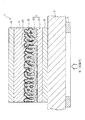
図1に示す光電変換素子1は、電解質溶液を必要としない、いわゆる乾式光電変換素子と呼ばれるものである。この光電変換素子1は、基板2と、第1の電極3と、緻密質層(緻密質な電子輸送層)41と、多孔質層(多孔質な電子輸送層)42と、色素層Dと、正孔輸送層5と、第2の電極6とが、この順で積層されている。以下、各層(各部)の構成について説明する。
基板2は、第1の電極3、緻密質層41、多孔質層42、色素層D、正孔輸送層5および第2の電極6の各層を支持するものであり、平板状(または層状)の部材で構成されている。
【0019】
本実施形態の光電変換素子1では、図1および図2に示すように、基板2および後述する第1の電極3側から、例えば、太陽光等の光(以下、単に「光」と言う。)を入射させて(照射して)使用するものである。このため、基板2および第1の電極3は、それぞれ、好ましくは実質的に透明(無色透明、着色透明または半透明)とされる。これにより、光を、後述する色素層Dに効率よく到達させることができる。
この基板2の構成材料としては、例えば、各種ガラス材料、各種セラミックス材料、ポリカーボネート(PC)、ポリエチレンテレフタレート(PET)のような各種樹脂材料等が挙げられる。また、基板2は、単層または複数層の積層体で構成されていてもよい。
【0020】
基板2の平均厚さは、材料、用途等により適宜設定され、特に限定されないが、例えば、次のようにすることができる。
基板2が硬質なものである場合、その平均厚さは、0.1〜1.5mm程度であるのが好ましく、0.8〜1.2mm程度であるのがより好ましい。また、基板2が可撓性(フレキシブル性)を有するものである場合、その平均厚さは、0.5〜150μm程度であるのが好ましく、10〜75μm程度であるのがより好ましい。
なお、例えば、光電変換素子1を各種の電子機器に搭載する場合、電子機器の構成部材を光電変換素子1の基板2として利用することができる。
【0021】
基板2の上面には、層状の第1の電極3が設けられている。
第1の電極3の構成材料には、例えば、インジウムティンオキサイド(ITO)、フッ素ドープした酸化錫(FTO)、酸化インジウム(IO)、酸化錫(SnO2)のような各種金属酸化物(透明導電性酸化物)、アルミニウム、ニッケル、コバルト、白金、銀、金、銅、モリブデン、チタン、タンタルまたはこれらを含む合金のような各種金属材料、黒鉛のような各種炭素材料等が挙げられ、これらのうちの1種または2種以上を組み合わせて用いることができる。
【0022】
第1の電極3の平均厚さは、材料、用途等により適宜設定され、特に限定されないが、例えば、次のようにすることができる。
第1の電極3を各種金属酸化物で構成する場合、その平均厚さは、0.05〜5μm程度であるのが好ましく、0.1〜1.5μm程度であるのがより好ましい。また、第1の電極3を各種金属材料や各種炭素材料で構成する場合、その平均厚さは、0.01〜1μm程度であるのが好ましく、0.03〜0.1μm程度であるのがより好ましい。
【0023】
第1の電極3の上面には、電子輸送層4が設けられている。本実施形態では、この電子輸送層4は、第1の電極3側に設けられた緻密質層41と、この緻密質層41と接触するようにして、緻密質層41の上面に設けられた多孔質層42とで構成されている。この電子輸送層4は、後述する色素層Dで発生した電子を補足し、輸送する機能を有する。
【0024】
電子輸送層4の構成材料としては、例えば、二酸化チタン(TiO2)、一酸化チタン(TiO)、三酸化二チタン(Ti2O3)等の酸化チタン、酸化亜鉛(ZnO)、酸化スズ(SnO2)、SrTiO3、SiO2、Al2O3、SnO2のような酸化物、TiC、SiCのような炭化物、Si3N4、B4N、BNのような窒化物、CdSのような硫化物、CdSeのようなセレン化物のような各種n型半導体材料が挙げられ、これらのうちの1種または2種以上を組み合わせて用いることができる。これらの中でも、電子輸送層4の構成材料としては、酸化チタン(特に、二酸化チタン)を用いるのが好ましい。すなわち、電子輸送層4は、二酸化チタンを主材料とするものが好適である。
【0025】
二酸化チタンは、特に、電子の輸送能力に優れる。また、二酸化チタンは、光に対する感受性が高く、二酸化チタンを主材料として電子輸送層4を構成することにより、電子輸送層4自体でも、電子を発生させることができる。これにより、光電変換素子1の光電変換効率(発電効率)をより向上させることができる。また、二酸化チタンは、その結晶構造が安定しているので、二酸化チタンを主材料とする電子輸送層4は、過酷な環境下に曝された場合でも、経年変化(劣化)が少なく、安定した性能が長期間継続して得られるという利点を有する。
【0026】
さらに、二酸化チタンとしては、アナターゼ型の二酸化チタン、ルチル型の二酸化チタン、または、これらの混合物を用いることができる。なお、二酸化チタンとして、アナターゼ型の二酸化チタンとルチル型の二酸化チタンとの混合物を用いる場合、これらの混合比は、特に限定されないが、重量比で95:5〜5:95程度とするのが好ましく、80:20〜20:80程度とするのがより好ましい。
【0027】
緻密質層41は、その空孔率が多孔質層42の空孔率より小さく設定されている。この緻密質層41は、後述する正孔輸送層5と第1の電極3とが接触するのを防止または抑制する機能を有する。この緻密質層41を設けることにより、光電変換素子1の光電変換効率(エネルギー変換効率)が低下するのを防止することができる。
【0028】
一方、多孔質層42は、その空孔率が比較的大きく設定されており、図2に示すように、複数の空孔421を有している。この多孔質層42には、後述するように、色素層Dが接触するように設けられるが、多孔質層42を複数の空孔421を有する形状とすることにより、色素層Dを多孔質層42の外面および空孔421の内面に沿って形成することができる。
【0029】
このため、色素層Dと多孔質層42との接触面積を十分に確保することができる。これにより、色素層Dで発生した電子を電子輸送層4へより効率よく伝達させることができる。また、多孔質層42に入射した光は、多孔質層42の内部まで侵入し、多孔質層42を透過、または、空孔421内で任意の方向に反射(乱反射、拡散等)して、より高い確率で色素層D中の色素に吸収されることになり、色素層Dでは、より効率よく電子および正孔が発生することになる。このようなことから、光電変換素子1の光電変換効率(エネルギー変換効率)をより向上させることができる。
【0030】
緻密質層41および多孔質層42に、それぞれ、それらの機能を如何なく発揮させる観点からは、緻密質層41および多孔質層42の条件を、次のように設定するのが好ましい。
緻密質層41の空孔率をA[%]とし、多孔質層42の空孔率をB[%]としたとき、B/Aは、1.1以上であるのが好ましく、5以上であるのがより好ましく、10以上であるのがさらに好ましい。
具体的には、緻密質層41の空孔率Aは、20%未満であるのが好ましく、5%未満であるのがより好ましく、2%未満であるのがさらに好ましい。一方、多孔質層42は、20%以上であるのが好ましく、20〜50%程度であるのがより好ましく、20〜40%程度であるのがさらに好ましい。
【0031】
また、緻密質層41と多孔質層42との厚さの比率は、特に限定されないが、1:99〜60:40程度であるのが好ましく、10:90〜40:60程度であるのがより好ましい。
具体的には、緻密質層41の平均厚さは、0.01〜10μm程度であるのが好ましく、0.1〜5μm程度であるのがより好ましい。一方、多孔質層42の平均厚さは、0.1〜300μm程度であるのが好ましく、0.5〜100μm程度であるのがより好ましく、1〜25μm程度であるのがさらに好ましい。
【0032】
また、緻密質層41と多孔質層42との界面は、不明確であること、すなわち、緻密質層41と多孔質層42とは、互いに部分的に重なりあった状態であることが好ましい。これにより、多孔質層42から緻密質層41へ電子をより確実に伝達させることができる。
なお、例えば、後述する正孔輸送層5の構成材料の種類等によっては、緻密質層41は、省略することもできる。すなわち、電子輸送層4は、図示の構成と異なり、その全体が多孔質なものであってもよい。また、例えば、電子輸送層4は、その厚さ方向の途中に緻密質層41を有する構成であってもよい。
【0033】
色素層Dは、多孔質層42に接触するように設けられている。この色素層Dは、主として色素で構成され、多孔質層42の外面および空孔421の内面に沿って形成されている。
この色素層D(色素)は、受光により電子と正孔とを発生する。このうち、電子は、前記の電子輸送層4へ、また、正孔は、後述する正孔輸送層5へ、それぞれ伝達される。
【0034】
この色素には、例えば、各種顔料や各種染料を単独または混合して使用することができるが、経時的変質(劣化)が少ないという点で顔料を、電子輸送層4(多孔質層42)への吸着性に優れるという点で染料を用いるのが好ましい。
顔料としては、例えば、フタロシアニン系顔料、アゾ系顔料、アントラキノン系顔料、アゾメチン系顔料、キノフタロン系顔料、イソインドリン系顔料、ニトロソ系顔料、ペリノン系顔料、キナクリドン系顔料、ペリレン系顔料、ピロロピロール系顔料、ジオキサジン系顔料のような各種有機顔料、炭素系顔料、クロム酸塩系顔料、硫化物系顔料、酸化物系顔料、水酸化物系顔料、フェロシアン化物系顔料、ケイ酸塩系顔料、リン酸塩系顔料、その他(例えば硫化カドミウム、セレン化カドミウム等)のような各種無機顔料等が挙げられる。
【0035】
また、染料としては、例えば、RuL2(SCN)2、RuL2Cl2、RuL2(CN)2、Rutenium535−bisTBA(Solaronics社製)、[RuL2(NCS)2]2H2Oのような金属錯体色素、シアン系色素、キサンテン系色素、アゾ系色素、ハイビスカス色素、ブラックベリー色素、ラズベリー色素、ザクロ果汁色素、クロロフィル色素等が挙げられる。なお、前記組成式中のLは、2,2’ーbipyridine、または、その誘導体を示す。
【0036】
色素層Dが形成された電子輸送層4の上面には、色素層Dに接触するように層状の正孔輸送層5が設けられている。この正孔輸送層5は、色素層Dで発生した正孔を捕捉し、輸送する機能を有する。
正孔輸送層5の構成材料としては、例えば、各種イオン伝導特性を有する物質、トリフェニルジアミン(モノマー、ポリマー等)、ポリアニリン、ポリピロール、ポリチオフェン、フタロシアニン化合物(例えば、銅フタロシアニン)またはこれらの誘導体のような各種p型半導体材料が挙げられ、これらのうちの1種または2種以上を組み合わせて用いることができる。これらの中でも、正孔輸送層5の構成材料としては、特に、イオン伝導特性を有する物質(イオン伝導性物質)が好ましい。すなわち、正孔輸送層5は、イオン伝導特性を有する物質を主材料とするものが好適である。イオン伝導特性を有する物質を主材料として正孔輸送層5を構成することにより、正孔輸送層5は、色素層Dで発生した正孔(ホール)をより効率よく補足し、輸送することができるようになる。これにより、光電変換素子1の光電変換効率(発電効率)をより向上させることができる。
【0037】
また、イオン伝導特性を有する物質としては、例えば、CuI、AgIのようなヨウ化物、AgBrのような臭化物等のハロゲン化物、CuSCNのようなチオシアン酸塩(ロダン化物)等が挙げられ、これらのうちの1種または2種以上を組み合わせて用いることができる。これらの中でも、イオン伝導特性を有する物質としては、ヨウ化物、臭化物等のハロゲン化物が好ましく、ヨウ化物がより好ましい。ハロゲン化物(特に、ヨウ化物)は、特に正孔の輸送能力に優れている。このため、ヨウ化物を主材料として正孔輸送層5を構成することにより、光電変換素子1の光電変換効率をより向上させることができる。
【0038】
また、正孔輸送層5は、図2に示すように、色素層Dが形成された多孔質層42の空孔421内に入り込んで形成され、色素層Dと正孔輸送層5との接触面積が十分に確保されている。このため、色素層Dで発生した正孔(ホール)を正孔輸送層5へより効率よく伝達させることができる。
正孔輸送層5の平均厚さは、特に限定されないが、1〜500μm程度であるのが好ましく、10〜300μm程度であるのがより好ましく、10〜30μm程度であるのがさらに好ましい。
【0039】
正孔輸送層5の上面には、層状の第2の電極6が設けられている。
この第2の電極6の構成材料としては、例えば、アルミニウム、ニッケル、コバルト、白金、銀、金、銅、モリブデン、チタン、タンタルまたはこれらを含む合金のような各種金属材料、あるいは、黒鉛のような各種炭素材料等が挙げられ、これらのうちの1種または2種以上を組み合わせて用いることができる。その他、第2の電極6の構成材料には、各種透明導電性酸化物を用いることもできる。
第2の電極6の平均厚さは、材料、用途等により適宜設定され、特に限定されないが、0.01〜5μm程度であるのが好ましく、0.03〜1.5μm程度であるのがより好ましい。
【0040】
以上のような構成の光電変換素子1に、基板2側から光が入射すると、主に色素層D(色素)において電子が励起され、電子(e−)と正孔(h+)とが発生する。このうち、電子は、電子輸送層4へ、正孔は、正孔輸送層5へ伝達され、各層中を輸送される。これにより、第1の電極3と第2の電極6との間に電位差(光起電力)が生じる。そして、光電変換素子1の第1の電極3と第2の電極6とを外部回路8により接続すると、外部回路8に電流(光励起電流)が流れる。
【0041】
このような光電変換素子1では、図1に示すように、第1の電極3、緻密質層41、多孔質層42、色素層D、正孔輸送層5および第2の電極6の各層が、それぞれ、アルファベット大文字「E」の形状(所定の情報を表示する形状)に形成されている。以下、かかるアルファベット大文字「E」の形状に形成された部分を「表示形状部X」と言う。
【0042】
前述したように、光電変換素子1は、基板2側から光を入射させて使用される。すなわち、光電変換素子1は、基板2の下面(図1中下側の面)が前面となるようにして使用される。このため、光電変換素子1の使用状態では、アルファベット大文字「E」なる表示形状部Xが視認されることになる。したがって、光電変換素子1は、デザイン性に優れたものとなる。
この表示形状部Xの平面視での面積は、用途等により適宜設定され、特に限定されないが、200〜10000mm2程度であるのが好ましく、500〜1000mm2程度であるのがより好ましい。これにより、光電変換素子1の光電変換効率をより向上させることができる。
【0043】
また、このような光電変換素子1には、図2および図3に示すように、基板2の下面(第1の電極3と反対側の面)に、表示形状部Xの輪郭を縁取りする帯状の装飾部7が設けるようにしてもよい。装飾部7を設けることにより、表示形状部Xの輪郭をより鮮明にすることができる。これにより、表示形状部Xを、基板2側からより明確に視認することができ、光電変換素子1の情報の表示またはデザインの構成上、有効である。
【0044】
この装飾部7の色と表示形状部Xの色とは、明度の差が大きくなるよう選択するのが好ましく、例えば、補色の関係にある色の組み合わせや、濃淡が異なる同系色の組み合わせ等を選択することができる。
装飾部7の構成材料としては、例えば、各種金属材料、各種樹脂材料、各種セラミックス材料等が挙げられる。
なお、装飾部7は、図4に示すように、表示形状部Xに対応する部分を残して、基板2の下面全体を覆うように設けられていてもよい。
【0045】
以下、本発明の光電変換素子の製造方法について、詳細に説明する。
本発明では、第1の電極3、緻密質層41、多孔質層42、色素層D、正孔輸送層5および第2の電極6のうちの少なくとも1つを、印刷法を用いて、所定の情報を表示する部分または所定のデザインを構成する部分を有する形状に形成することに特徴を有する。これにより、大掛かりな設備を必要とせず、微細な形状を高精度で形成することができる。
【0046】
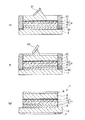
図5および図6は、それぞれ、本発明の光電変換素子の製造方法を説明するための図(縦断面図)である。なお、以下の説明では、図5および図6中の紙面上、上側を「上」または「上方」、下側を「下」または「下方」と言い、各層(各部材)の上側の面を「上面」、下側の面を「下面」と言う。
本実施形態では、光電変換素子1の各層(第1の電極3、緻密質層41、多孔質層42、色素層D、正孔輸送層5および第2の電極6)が、それぞれ、印刷法を用いて、表示形状部Xの形状に形成されている。
【0047】
印刷法では、図5および図6に示すように、表示形状部Xの形状をなす貫通孔901を有するマスク90が用いられる。
本実施形態では、マスク90を基板2に固定して、スキージ91により、印刷法を用いて形成すべき層の構成材料またはその前駆体を含む液体を掃いて、貫通孔901内に供給して、前記の各層を形成する。
用いる液体の粘度(常温)は、特に限定されないが、通常、10〜40cps程度であるのが好ましく、15〜30cps程度であるのがより好ましい。用いる液体の粘度をかかる範囲とすることにより、取り扱いが容易となる。
【0048】
また、マスク90は、表示形状部Xの形状に対応した形状の貫通孔901が形成されたものであれば、特に限定されないが、例えば、(I)エッチング、電鋳、レーザ加工、プレス加工等により所定の形状に形成された金属板、(II)プレス加工、カッティング加工等により所定の形状に形成された樹脂製不織布や樹脂フィルム等が好適に使用される。これらのものは、耐溶剤(耐薬品性)、耐熱性が良好であることから好ましい。
【0049】
金属板の構成材料としては、例えば、アルミニウムまたはアルミニウム合金、ステンレス、黄銅、洋白材等が挙げられる。
樹脂製不織布および樹脂フィルムの構成材料としては、それぞれ、例えば、ポリエステル、ポリオレフィン、ポリウレタン、ポリエチレンまたはこれらを主とする共重合体、ブレンド体、ポリマーアロイ等が挙げられる。
【0050】
また、図5および図6に示すように、マスク90は、感圧接着剤92により基板2の上面に固定(固着)される。これにより、マスク90と基板2との間隙が感圧接着剤92により封止されるので、この間隙から各層形成用の液体が流出するのを防止することができ、その結果、表示形状部Xの輪郭をより鮮明にすることができる。また、感圧接着剤92を用いれば、マスク90の設置および除去を容易に行うことができるという利点もある。
このような感圧接着剤92としては、例えば、アクリル系、シリコーン系、ポリエステル系、ポリウレタン系、ポリエーテル系、ゴム系等の各種のものが挙げられ、これらのうちの1種または2種以上を組み合わせて用いることができる。
なお、感圧接着剤92は、必要に応じて、省略することもできる。
【0051】
以下、光電変換素子1の製造方法の各工程について、順次説明する。
[1] 第1の電極3の形成
まず、基板2を用意する。この基板2には、厚さが均一で、たわみのないものが好適に用いられる。
この基板2の上面に、印刷法を用いて、第1の電極3形成用の液体を供給して、第1の電極3を形成する(図5(a)参照)。
【0052】
第1の電極3形成用の液体としては、例えば、次のようなものを用いることができる。
▲1▼:第1の電極3を各種金属酸化物、各種金属材料、各種炭素材料で構成する場合、第1の電極3形成用の液体としては、これらの材料で構成された粒子を含む分散液(懸濁液)を用いることができる。
この場合、第1の電極3形成用の液体中の粒子の含有量は、特に限定されないが、0.5〜25wt%程度であるのが好ましく、2〜15wt%程度であるのがより好ましい。
【0053】
用いる粒子の平均粒径は、特に限定されないが、1〜30nm程度であるのが好ましく、2〜10nm程度であるのがより好ましい。
また、粒子には、常温での凝集を阻止するための凝集阻止剤(分散剤)で被覆したものを用いるのが好ましい。この凝集阻止剤としては、例えば、アルキルアミンのような窒素原子を含む基を有する化合物、アルカンジオールのような酸素原子を含む基を有する化合物、アルキルチオール、アルカンジチオールのような硫黄原子を含む基を有する化合物等が挙げられる。
【0054】
また、この場合、第1の電極3形成用の液体中には、所定の処理(例えば、加熱等)により、凝集阻止剤を除去し得る除去剤が添加される。この除去剤としては、例えば、ギ酸、酢酸、プロピオン酸、ブタン酸、ヘキサン酸、オクチル酸のような炭素数1〜10の直鎖状または分岐状の飽和カルボン酸、アクリル酸、メタクリル酸、クロトン酸、ケイ皮酸、安息香酸、ソルビン酸のような不飽和カルボン酸、シュウ酸、マロン酸、セバシン酸、マレイン酸、フマル酸、イタコン酸のような二塩基酸等の各種カルボン酸類、これらのカルボン酸類のカルボキシル基をリン酸基やスルホニル基に置換した各種リン酸類や各種スルホン酸類等の有機酸、または、その有機酸エステル、その他、無水フタル酸、無水トリメリット酸、無水ピロメリット酸、無水ベンゾフェノンテトラカルボン酸、エチレングリコールビス(アンヒドロトリメリテート)、グリセロールトリス(アンヒドロトリメリテート)のような芳香族酸無水物、無水マレイン酸、無水コハク酸、テトラヒドロ無水フタル酸、メチルテトラヒドロ無水フタル酸、無水メチルナジック酸、アルケニル無水コハク酸、ヘキサヒドロ無水フタル酸、メチルヘキサヒドロ無水フタル酸、メチルシクロヘキセンテトラカルボン酸無水物のような環状脂肪族酸無水物、ポリアジピン酸無水物、ポリアゼライン酸無水物、ポリセバシン酸無水物などの脂肪族酸無水物等を挙げることができる。
分散媒には、例えば、テルピネオール、ミネラルスピリット、キシレン、トルエン、エチルベンゼン、メシチレン、ヘキサン、ヘプタン、オクタン、デカン、ドデカン、シクロヘキサン、シクロオクタンまたはこれらを含む混合液を用いることができる。
【0055】
また、第1の電極3形成用の液体中には、フェノール樹脂、エポキシ樹脂、不飽和ポリエステル樹脂、ビニルエステル樹脂、ジアリルフタレート樹脂、オリゴエステルアクリレート樹脂、キシレン樹脂、ビスマレイミドトリアジン樹脂、フラン樹脂、ユリア樹脂、ポリウレタン樹脂、メラミン樹脂、シリコーン樹脂のような各種熱硬化性樹脂の前駆体が添加(混合)されていてもよい。
なお、このような第1の電極3形成用の液体の粘度は、例えば、粒子の含有量、分散媒の種類や組成、添加物の有無や種類等を適宜設定することにより調整することができる。
【0056】
▲2▼:第1の電極3を各種金属材料で構成する場合、第1の電極3形成用の液体としては、各種金属材料の前駆体である金属錯体等で構成された金属塩と、還元剤とを含む分散液(懸濁液)を用いることができる。
この場合、第1の電極3形成用の液体中の金属の含有量は、特に限定されないが、0.1〜5wt%程度であるのが好ましく、0.5〜2wt%程度であるのがより好ましい。
成形される粒子の平均粒径は、特に限定されないが、10〜100nm程度であるのが好ましく、30〜70nm程度であるのがより好ましい。
【0057】
また、還元剤としては、例えば、ブドウ糖、果糖、ヒドラジン、ホルマリン等が挙げられる。
分散媒には、例えば、メタノール、エタノール、水、エチレングリコール、グリセリン等またはこれらを含む混合液を用いることができる。
なお、このような第1の電極3形成用の液体の粘度は、例えば、金属の含有量、分散媒の種類や組成等を適宜設定することにより調整することができる。
【0058】
▲3▼:第1の電極3を各種金属酸化物で構成する場合、第1の電極3形成用の液体としては、各種金属酸化物の前駆体を含む溶液を用いることができる。
用いる金属酸化物の前駆体としては、例えば、金属アルコキシド、酢酸または酢酸誘導体の金属塩のような有機金属化合物、金属塩化物、金属硫化物、金属シアン化物等の無機金属化合物等が挙げられ、これらのうちの1種または2種以上を組み合わせて用いることができる。
第1の電極3形成用の液体中の金属酸化物の前駆体の濃度(含有量)は、特に限定されないが、0.5〜25wt%程度であるのが好ましく、2〜15wt%程度であるのがより好ましい。
【0059】
また、溶媒には、例えば、水、エチレングリコール、グリセリン、ジエチレングリコール、トリエタノールアミンのような多価アルコール、メタノール、エタノール、イソプロパノール、ブタノール、アリルアルコール、フルフリルアルコール、エチレングリコールモノアセタートのような単価アルコールまたはこれらを含む混合液を用いることができる。
なお、このような第1の電極3形成用の液体の粘度は、例えば、金属酸化物の前駆体の濃度、溶媒の種類や組成等を適宜設定することにより調整することができる。
【0060】
基板2の上面に、マスク90を感圧接着剤92を介して固定する。このマスク90を用いて、第1の電極3形成用の液体をスキージ91で掃くことにより、貫通孔901内に供給して、膜(薄膜または厚膜)を形成する。
次いで、マスク90を除去した後、膜に対して、例えば、熱処理や、紫外線、電子線、放射線等の照射を行う。
必要に応じて、以上のような操作を繰り返し行って、所望の厚さの第1の電極3を形成する。
【0061】
[2] 電子輸送層4の形成
次に、第1の電極3の上面に、電子輸送層4を形成する。以下では、主として二酸化チタンで構成される電子輸送層4を形成する場合を一例として説明する。
[2−1] 緻密質層41の形成
まず、第1の電極3の上面に、印刷法を用いて、緻密質層41形成用の液体を供給して、緻密質層41を形成する(図5(b)参照)。
【0062】
緻密質層41形成用の液体としては、例えば、二酸化チタンの前駆体を含む溶液を用いることができる。
二酸化チタンの前駆体としては、例えば、チタンテトライソプロポキシド(TPT)、チタンテトラメトキシド、チタンテトラエトキシド、チタンテトラブトキシド等のチタンアルコキシド、チタンオキシアセチルアセトナート(TOA)のような有機チタン化合物や、四塩化チタン(TTC)のような無機チタン化合物等が挙げられ、これらのうちの1種または2種以上を混合して用いることができる。
【0063】
緻密質層41形成用の液体中の二酸化チタンの前駆体の濃度(含有量)は、特に限定されないが、0.1〜10mol/L程度であるのが好ましく、0.5〜5mol/L程度であるのがより好ましい。
また、溶媒には、例えば、無水エタノール、2−ブタノール、2−プロパノール、2−n−ブトキシエタノール、プロピレングリコール、モノブチルエーテルまたはこれらを含む混合液を用いることができる。
【0064】
なお、二酸化チタンの前駆体としてチタンアルコキシドを用いる場合、緻密質層41形成用の液体中には、例えば、四塩化チタン、酢酸、アセチルアセトン、トリエタノールアミン等の各種添加物を添加するのが好ましい。これにより、チタンアルコキシドの加水分解反応を抑止することができる。この添加物とチタンアルコキシドとの配合比は、特に限定されないが、モル比で1:2〜8:1程度とするのが好ましい。
【0065】
なお、このような緻密質層41形成用の液体の粘度は、例えば、二酸化チタンの前駆体の濃度、溶媒の種類や組成、添加物の有無、種類、組成や濃度等を適宜設定することにより調整することができる。
基板2の上面に、前記工程[1]で用いたマスク90より厚さの厚いマスク90を感圧接着剤92を介して固定する。このマスク90を用いて、緻密質層41形成用の液体をスキージ91で掃くことにより、貫通孔901内に供給して、膜(薄膜または厚膜)を形成する。
【0066】
次いで、マスク90を除去した後、膜に対して熱処理(乾燥)を施す。これにより、前記溶媒を揮発させ、除去する。この熱処理の条件は、好ましくは50〜250℃×1〜60分程度、より好ましくは100〜200℃×5〜30分程度とされる。また、熱処理の雰囲気は、例えば、大気、窒素ガス、不活性ガス、真空または減圧状態のような非酸化性雰囲気等とすることができる。
【0067】
さらに、膜に対して、前記熱処理より高温での熱処理(焼成)を施す。これにより、膜中に残存する有機成分(溶媒や添加物等)を除去することができるとともに、アモルファス状態またはアナターゼ型の二酸化チタンが生成する。この熱処理の条件は、好ましくは300〜700℃×1〜70分程度、より好ましくは400〜550℃×5〜45分程度とされる。また、熱処理の雰囲気は、前記と同様の雰囲気とすることができる。
【0068】
なお、基板2として、主として樹脂材料で構成されるもの(可撓性基板)を用いる場合には、前記膜に対して、水熱合成処理(水熱処理)を施すのが好ましい。
ここで、水熱合成処理とは、前記膜を高圧水蒸気(飽和水蒸気)で処理することを言う。具体的には、水熱合成処理は、前記膜が形成された基材を、少量の水とともに密閉容器内に収納し、密閉容器を加熱することにより行われる。加熱により密閉容器内では、水が水蒸気となり、密閉容器内の圧が上昇する。この高圧水蒸気により、膜中に存在する有機成分が除去されるとともに、二酸化チタンの前駆体に加水分解反応が進行して、アモルファス状態の二酸化チタンが生成する。かかる水熱合成処理によれば、水が蒸発する程度の比較的低い温度(例えば、100〜200℃程度)で、前記膜の処理を行うことができるという利点がある。
【0069】
必要に応じて、以上のような操作を繰り返し行って、所望の厚さの緻密質層41を形成する。
なお、緻密質層41の形成に先立って、第1の電極3の上面には、例えば、O2プラズマ処理、EB処理、有機溶剤(例えばエタノール、アセトン等)での洗浄処理等を行うことにより、第1の電極3の上面に付着した有機物を除去するようにしてもよい。
【0070】
[2−2] 多孔質層42の形成
次に、緻密質層41の上面に、印刷法を用いて、多孔質層42形成用の液体を供給して、多孔質層42を形成する(図5(c)参照)。
多孔質層42形成用の液体としては、例えば、二酸化チタン粉末と二酸化チタンの前駆体とを含む分散液(ゾル液)を用いることができる。これにより、前述したような構成の多孔質層42を比較的容易に得ることができる。
用いる二酸化チタン粉末(粒子)としては、アナターゼ型の二酸化チタン粉末単独、ルチル型の二酸化チタン粉末単独またはこれらの混合物のいずれであってもよい。
【0071】
二酸化チタン粉末の平均粒径は、特に限定されないが、1nm〜1μm程度であるのが好ましく、1〜100nm程度であるのがより好ましく、5〜50nm程度であるのがさらに好ましい。これにより、二酸化チタン粉末を多孔質層42形成用の液体中により均一に分散させることができ、多孔質層42の空孔形態(例えば、空孔率、空孔の分布等)の制御が容易となる。
【0072】
また、アナターゼ型の二酸化チタン粉末とルチル型の二酸化チタン粉末とを混合して用いる場合、これらの2種類の粉末は、それらの平均粒径が異なっていてもよいし、同じであってもよい。
多孔質層42形成用の液体中の二酸化チタン粉末の含有量は、特に限定されないが、0.1〜10wt%程度であるのが好ましく、0.5〜5wt%程度であるのがより好ましい。
【0073】
多孔質層42形成用の液体は、次のようにして調製することができる。
すなわち、まず、前述した緻密質層41形成用の液体と同様の液体を用意する。なお、この液体中の二酸化チタンの前駆体の濃度(含有量)は、特に限定されないが、0.1〜3mol/L程度であるのが好ましく、0.5〜2mol/L程度であるのがより好ましい。
【0074】
次に、この液体に水を混合する。この水と二酸化チタンの前駆体との配合比は、特に限定されないが、モル比で1:4〜4:1程度とするのが好ましい。
次に、この混合液に、二酸化チタン粉末を混合することにより、多孔質層42形成用の液体を得る。また、この多孔質層42形成用の液体は、必要に応じて、例えば、前記緻密質層41形成用の液体に用いる溶媒を用いて希釈して用いるようにしてもよい。
なお、このような多孔質層42形成用の液体の粘度は、例えば、二酸化チタン粉末の含有量、二酸化チタンの前駆体の濃度、溶媒の種類や組成、添加物の有無、種類、組成や濃度、希釈の程度(希釈倍率)等を適宜設定することにより調整することができる。
【0075】
基板2の上面に、前記工程[2−1]で用いたマスク90より厚さの厚いマスク90を感圧接着剤92を介して固定する。このマスク90を用いて、緻密質層41形成用の液体をスキージ91で掃くことにより、貫通孔901内に供給して、膜(薄膜または厚膜)を形成する。
この際、緻密質層41を加熱しつつ、緻密質層41の上面に多孔質層42形成用の液体を供給するのが好ましい。この加熱温度としては、特に限定されないが、80〜180℃程度であるのが好ましく、100〜160℃程度であるのがより好ましい。
【0076】
次いで、この膜に、必要に応じて、熱処理(例えば、焼成等)を施してもよい。この熱処理の条件としては、例えば、温度250〜500℃×0.5〜3時間程度とするのが好ましい。
また、基板2として、主として樹脂材料で構成されるもの(可撓性基板)を用いる場合には、この熱処理に代えて、前述したような水熱合成処理(水熱処理)を行うようにしてもよい。
必要に応じて、以上のような操作を繰り返し行って、所望の厚さの多孔質層42を形成する。
【0077】
[3] 色素層Dの形成
次に、多孔質層42(電子輸送層4)の上面に、印刷法を用いて、色素層D形成用の液体を供給して、色素層Dを形成する(図5(d)参照)。
色素層D形成用の液体としては、例えば、色素を含む溶液または分散液(懸濁液)を用いることができる。
色素層D形成用の液体中の色素の濃度(含有量)は、特に限定されないが、0.01〜1wt%程度であるのが好ましく、0.05〜0.1wt%程度であるのがより好ましい。
【0078】
また、溶媒または分散媒には、例えば、水、メタノール、エタノール、イソプロパノール、アセトニトリル、酢酸エチル、エーテル、塩化メチレン、NMP(N−メチル−2−ピロリドン)、グリセリン、ポリエチレングリコール、モノブチルエーテルまたはこれらを含む混合液を用いることができる。
なお、このような色素層D形成用の液体の粘度は、例えば、色素の濃度、溶媒または分散媒の種類や組成等を適宜設定することにより調整することができる。
【0079】
基板2の上面に、前記工程[2−2]で用いたマスク90より厚さの厚いマスク90を感圧接着剤92を介して固定する。このマスク90を用いて、色素層D形成用の液体をスキージ91で掃くことにより、貫通孔901内に供給して、膜(薄膜または厚膜)を形成する。
次いで、マスク90を除去した後、例えば、自然乾燥による方法や、空気、窒素ガス等の気体を吹き付ける方法等により溶媒を除去する。さらに、必要に応じて、例えば、60〜100℃×0.5〜2時間程度等の熱処理等を施すことにより乾燥してもよい。これにより、色素は、多孔質層42の外面および空孔421の内面に、例えば、吸着(化学吸着)、結合(共有結合、配位結合)等する。
必要に応じて、以上のような操作を繰り返し行って、所望の厚さの色素層Dを形成する。
【0080】
[4] 正孔輸送層5の形成
次に、色素層Dが形成された多孔質層42(電子輸送層4)の上面に、印刷法を用いて、正孔輸送層5形成用の液体を供給して、正孔輸送層5を形成する(図6(e)参照)。以下では、主としてイオン伝導特性を有する物質(イオン伝導性物質)で構成される正孔輸送層5を形成する場合を一例として説明する。
【0081】
正孔輸送層5形成用の液体としては、例えば、イオン伝導特性を有する物質を含む溶液を用いることができる。
正孔輸送層5形成用の液体中のイオン伝導特性を有する物質の濃度(含有量)は、特に限定されないが、5×10⁻⁴〜0.1mol/L程度であるのが好ましく、5×10−3〜5×10−2mol/L程度であるのがより好ましい。
また、溶媒には、例えば、水、アセトニトリル、エタノール、メタノール、イソプロピルアルコール、グリセリン、ポリエチレングリコール、モノブチルエーテルまたはこれらを含む混合液を用いることができるが、これらの中でも、特に、アセトニトリルが好ましい。
【0082】
なお、正孔輸送層5の構成材料として、イオン伝導特性を有する物質を用いる場合、正孔輸送層5形成用の液体中には、バインダーとして、例えばシアノレジン等のシアノエチル化物を添加するのが好ましい。この場合、正孔輸送層5形成用の液体中のシアノエチル化物の濃度(含有量)は、特に限定されないが、1×10⁻⁶〜10wt%程度とするのが好ましく、1×10⁻⁴〜1×10⁻²wt%程度とするのがより好ましい。
また、正孔輸送層5形成用の液体中には、正孔の輸送効率を向上させる機能を有する正孔輸送効率向上物質を添加するのが好ましい。これにより、正孔輸送層5のキャリア移動度(正孔輸送能)をより向上させることができる。
【0083】
この正孔輸送効率向上物質としては、例えば、ハロゲン化アンモニウム等の各種ハロゲン化物を用いることができるが、特に、テトラプロピルアンモニウムヨーダイド(TPAI)が好適である。
正孔輸送層5形成用の液体中の正孔輸送効率向上物質の濃度(含有量)は、特に限定されないが、1×10⁻⁴〜1×10⁻¹wt%程度であるのが好ましく、1×10⁻⁴〜1×10⁻²wt%程度であるのがより好ましい。これにより、前記効果をより向上させることができる。
【0084】
さらに、正孔輸送層5形成用の液体中には、イオン伝導特性を有する物質が結晶化する際に、その結晶サイズが増大するのを抑制する結晶サイズ粗大化抑制物質を添加するのが好ましい。これにより、イオン伝導特性を有する物質は、結晶化する際に結晶サイズが増大するのが防止または抑制される。このため、電子輸送層4でのクラックの発生、色素層Dと正孔輸送層5との接触性の低下等の不都合を好適に防止することができる。その結果、光電変換素子1の光電変換効率等の特性が低下(劣化)するのを防止することができる。
【0085】
この結晶サイズ粗大化抑制物質としては、例えば、前述したシアノエチル化物、正孔輸送効率向上物質の他、例えば、チオシアン酸ナトリウム(NaSCN)、チオシアン酸カリウム(KSCN)、チオシアン酸銅(CuSCN)、チオシアン酸アンモニウム(NH4SCN)のようなチオシアン酸塩(ロダン化物)等のうちの1種または2種以上を組み合わせて用いることができる。
【0086】
正孔輸送層5形成用の液体中の結晶サイズ粗大化抑制物質の濃度(含有量)は、特に限定されないが、1×10− 6〜10wt%程度であるのが好ましく、1×10⁻⁴〜1×10⁻²wt%程度であるのがより好ましい。これにより、前記効果をより向上させることができる。
なお、このような正孔輸送層5形成用の液体の粘度は、例えば、正孔輸送層の構成材料の種類、組成や濃度、正孔輸送効率向上物質の種類や濃度、溶媒の種類や組成、添加物の有無、種類や濃度等を適宜設定することにより調整することができる。
【0087】
基板2の上面に、前記工程[3]で用いたマスク90より厚さの厚いマスク90を感圧接着剤92を介して固定する。このマスク90を用いて、正孔輸送層5形成用の液体をスキージ91で掃くことにより、貫通孔901内に供給して、膜(薄膜または厚膜)を形成する。
この際、色素層D(色素層Dが形成された多孔質層42)を加熱しつつ、色素層Dが形成された多孔質層42の上面に液滴70を着弾させる(供給する)のが好ましい。この加熱温度としては、特に限定されないが、50〜150℃程度であるのが好ましく、80〜100℃程度であるのがより好ましい。
必要に応じて、以上のような操作を繰り返し行って、所望の厚さの正孔輸送層5を形成する。
【0088】
[5] 第2の電極6の形成
次に、正孔輸送層5の上面に、印刷法を用いて、第2の電極6形成用の液体を供給して、第2の電極6を形成する(図6(f)参照)。
第2の電極6は、前記工程[1]と同様にして形成することができる。
【0089】
[6] 装飾部7の形成
次に、基板2の下面に、装飾部7を形成する(図6(g)参照)。
この装飾部7は、例えば、印刷法、インクジェット法等を用いる方法、シート状の部材を接着する方法、装飾金属部材を接着する方法等により形成することができる。
以上のような工程を経て、光電変換素子1が製造される。
【0090】
なお、本実施形態では、1個の光電変換素子1を単独で製造する場合について説明したが、本発明の光電変換素子の製造方法は、複数個の光電変換素子1を同時に製造した後、各光電変換素子1を切り離して製造する、いわゆる多数個取りに適用することもできる。
また、マスク90は、各工程[1]〜[5]毎に新たなものを使用するようにしてもよく、また、連続する2以上の工程において共通のものを使用するようにしてもよい。
【0091】
以上説明したような光電変換素子1では、表示形状部Xが1つ設けられている構成であったが、本発明では、表示形状部Xは、複数設けられていてもよい。
また、本実施形態の光電変換素子1では、第1の電極3、緻密質層41、多孔質層42、色素層D、正孔輸送層5および第2の電極6の各層が、ほぼ同一の形状をなし、表示形状部Xが構成されているが、本発明では、第1の電極3、緻密質層41、多孔質層42、色素層D、正孔輸送層5および第2の電極6のうちの少なくとも1つにより表示形状部Xが構成されていてもよい。すなわち、本発明では、第1の電極3、緻密質層41、多孔質層42、色素層D、正孔輸送層5および第2の電極6のうちの少なくとも1つが表示形状部Xの形状に形成されていればよい。なお、光電変換素子1をよりデザイン性に優れるものとする観点からは、色素層Dと、それ以外の層の少なくとも1つとを、表示形状部Xの形状に形成するのが好ましい。
【0092】
また、前記実施形態のように、表示形状部Xの形状は、文字に限定されるものではなく、その他、記号、図形またはこれらの一部を構成するセグメントのような所定の情報を表示する形状や、所定のデザインを構成する形状であってもよい。
さらに、前記実施形態では、各層は、その全体が表示形状部Xの形状に形成されていたが、表示形状部Xの形状を一部に有するような構成であってもよい。
【0093】
本発明の電子機器は、このような光電変換素子1を備えるものである。
以下、図7および図8に基づいて、本発明の電子機器について説明する。
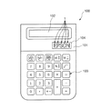
図7は、本発明の電子機器を適用した電卓を示す平面図、図8は、本発明の電子機器を適用した携帯電話機(PHSも含む)を示す斜視図である。
図7に示す電卓100は、本体部101と、本体部101の上面(前面)に設けられた表示部102、複数の操作ボタン103および光電変換素子設置部104とを備えている。
【0094】
図7に示す構成では、光電変換素子設置部104には、アルファベット大文字「E」、「P」、「S」、「O」、「N」なる表示形状部Xを、それぞれ備える光電変換素子1が5つ直列に接続されて配置されている。
これにより、光電変換素子1を電源として利用するとともに、情報を表示する要素として活用することができ、電卓100のデザイン性の向上を図ることができる。また、別途光電変換素子を設置する場所を省略することができ、有利である。
【0095】
図8に示す携帯電話機200は、本体部201と、本体部201の前面に設けられた表示部202、複数の操作ボタン203、受話口204、送話口205および光電変換素子設置部206とを備えている。
図8に示す構成では、光電変換素子設置部206が、表示部202の周囲を囲むようにして設けられ、平面視で正方形をなす表示形状部Xを備える光電変換素子1が複数、直列に接続されて配置されている。
【0096】
この場合、目立たない形で光電変換素子1を配置することができ、携帯電話機200のデザイン上の障害とならず、これにより、携帯電話機200をデザイン性に優れたものとすることができる。
また、光電変換素子1に、電源としての機能と情報を表示する機能とを併有させることにより、別途光電変換素子を設置する場所を省略することができ、有利である。
なお、本発明の電子機器としては、図7に示す電卓、図8に示す携帯電話機の他、例えば、光センサー、光スイッチ、電子手帳、電子辞書、腕時計、クロック等に適用することもできる。
【0097】
以上述べたように、本発明によれば、従来の光電変換素子のデザイン上の制約を開放し、デザイン性に優れる光電変換素子を得ることができる。
また、本発明の光電変換素子では、電源としての機能と情報を表示する機能(またはデザインを構成する機能)とを併有させることができるため、別途光電変換素子を設置する場所を省略することができる。このようなことから、本発明の光電変換素子は、特に、小型機器への適用に適している。
また、光電変換素子の配置個所、デザイン上の要請等に応じて、色素層の色を設定することにより、デザイン性の向上に有効である。
また、本発明の光電変換素子の製造方法によれば、光電変換素子を、安価かつ効率よく製造できる。
【0098】
以上、本発明の光電変換素子の製造方法、光電変換素子および電子機器について図示の実施形態について説明したが、本発明は、これに限定されるものではなく、各部の構成は、同様の機能を発揮する任意の構成と置換することができ、その他の構成(例えば、各層の間に、任意の目的の1層以上の層)が付加されていてもよい。
【図面の簡単な説明】
【図1】本発明の光電変換素子の実施形態を示す斜視図である。
【図2】図1中のA−A線断面図である。
【図3】図1に示す光電変換素子を下側から見た図である。
【図4】図1に示す光電変換素子を下側から見た図である。
【図5】本発明の光電変換素子の製造方法を説明するための図である。
【図6】本発明の光電変換素子の製造方法を説明するための図である。
【図7】本発明の電子機器を適用した電卓を示す平面図である。
【図8】本発明の電子機器を適用した携帯電話機を示す斜視図である。
【符号の説明】
1……光電変換素子 2……基板 3……第1の電極 4……電子輸送層 41……緻密質層 42……多孔質層 421……空孔 5……正孔輸送層 6……第2の電極 7……装飾部 8……外部回路 D……色素層 X……表示形状部 90……マスク 901……貫通孔 91……スキージ 92……感圧接着剤 100……電卓 101……本体部 102……表示部 103……操作ボタン 104……光電変換素子設置部 200……携帯電話機 201……本体部 202……表示部 203……操作ボタン 204……受話口 205……送話口 206……光電変換素子設置部[0001]
TECHNICAL FIELD OF THE INVENTION
The present invention relates to a method for manufacturing a photoelectric conversion element, a photoelectric conversion element, and an electronic device.
[0002]
[Prior art]
2. Description of the Related Art Conventionally, solar cells (photoelectric conversion elements) have attracted attention as environmentally friendly power supplies, and single-crystal silicon-type solar cells used for power supplies for artificial satellites and the like, and solar cells using polycrystalline silicon and amorphous silicon Is widely used for industry and home use. Recently, as a solar cell that can be manufactured at low cost without using a large-scale facility using inexpensive materials, a wet dye-sensitized solar cell (see Patent Document 1) and a dry dye-sensitized solar cell have been proposed. 2. Description of the Related Art A sensitive solar cell (see Patent Document 2) has been proposed.
[0003]
In general, these conventional solar cells cannot be freely designed, and may restrict the design of various devices on which the solar cells are mounted.
That is, conventional solar cells using silicon and dry dye-sensitized solar cells are all limited in shape to a square or the like, and there is no design freedom, and wet dye-sensitized solar cells are Since it has a structure for sealing the electrolyte, it cannot be formed into an arbitrary shape.
[0004]
Further, it is necessary to arrange a solar cell at a position where sunlight can be received for power generation, and to secure a light receiving area capable of securing a required power generation amount. For this reason, in a device equipped with a solar cell, the solar cell must be arranged in a relatively large area at a prominent position on the front surface, which greatly restricts the design of the device equipped with the solar cell. was there. Such a restriction is remarkable in a small device which cannot secure a large installation area for installing a solar cell.
[0005]
[Patent Document 1]
JP-A-2002-252040
[Patent Document 2]
JP-A-2002-314107
[0006]
[Problems to be solved by the invention]
An object of the present invention is to provide a method for manufacturing a photoelectric conversion element capable of obtaining a photoelectric conversion element having an excellent design, a photoelectric conversion element having an excellent design, and an electronic device including the photoelectric conversion element.
[0007]
[Means for Solving the Problems]
Such an object is achieved by the present invention described below.
The method for manufacturing a photoelectric conversion element of the present invention includes the steps of: forming a first electrode on a substrate;
Forming at least a partly porous electron transport layer on the first electrode;
Forming a dye layer to contact the electron transport layer;
Forming a hole transport layer to contact the dye layer,
Forming a second electrode on the hole transport layer, the method comprising the steps of:
At least one of the first electrode, the electron transport layer, the dye layer, the hole transport layer, and the second electrode is formed by using a printing method to display predetermined information or a predetermined portion. It is characterized in that it is formed in a shape having a part constituting a design.
Thereby, a photoelectric conversion element excellent in design can be obtained.
[0008]
In the method for manufacturing a photoelectric conversion element according to the aspect of the invention, the dye layer and at least one of the second electrode, the electron transport layer, the hole transport layer, and the first electrode may include the predetermined information. Is preferably formed in a shape having a portion for displaying a symbol or a portion constituting a predetermined design.
Thereby, a photoelectric conversion element having more excellent design properties can be obtained.
[0009]
The method for manufacturing a photoelectric conversion element of the present invention includes the steps of: forming a first electrode on a substrate;
Forming a dense electron transport layer on the first electrode;
Forming a porous electron transport layer to contact the dense electron transport layer;
Forming a dye layer to be in contact with the porous electron transport layer;
Forming a hole transport layer to contact the dye layer,
Forming a second electrode on the hole transport layer, the method comprising the steps of:
At least one of the first electrode, the dense electron transport layer, the porous electron transport layer, the dye layer, the hole transport layer, and the second electrode is formed using a printing method. And a portion having a portion for displaying predetermined information or a portion constituting a predetermined design.
Thereby, a photoelectric conversion element excellent in design can be obtained.
[0010]
In the method for manufacturing a photoelectric conversion element of the present invention, the dye layer, the first electrode, the dense electron transport layer, the porous electron transport layer, the hole transport layer, and the second electrode At least one of them is preferably formed in a shape having a portion for displaying the predetermined information or a portion constituting a predetermined design.
Thereby, a photoelectric conversion element having more excellent design properties can be obtained.
[0011]
In the method for manufacturing a photoelectric conversion element of the present invention, it is preferable that the mask used in the printing method is formed of a metal plate, a resin nonwoven fabric, or a resin film.
[0012]
In the method for manufacturing a photoelectric conversion element according to the aspect of the invention, it is preferable that the mask is fixed with a pressure-sensitive adhesive.
This makes it possible to sharpen the outline of a portion displaying predetermined information or a portion constituting a predetermined design, and to easily install and remove a mask.
[0013]
In the method for manufacturing a photoelectric conversion element according to the aspect of the invention, it is preferable that the predetermined information is a character, a number, a symbol, a graphic, or a segment forming a part thereof.
[0014]
In the method for manufacturing a photoelectric conversion element according to the present invention, after the step of forming the second electrode, a portion for displaying the predetermined information or a predetermined design is formed on a side of the substrate opposite to the first electrode. It is preferable to include a step of forming a decorative portion that borders the contour of the portion to be formed.
Thereby, the outline of a portion displaying predetermined information or a portion forming a predetermined design can be made clearer.
[0015]
The photoelectric conversion element of the present invention is characterized by being manufactured by the method for manufacturing a photoelectric conversion element of the present invention.
Thereby, a photoelectric conversion element excellent in design can be obtained.
[0016]
An electronic device according to the present invention includes the photoelectric conversion element according to the present invention.
Thereby, an electronic device having excellent design properties can be obtained.
[0017]
BEST MODE FOR CARRYING OUT THE INVENTION
Hereinafter, a method for manufacturing a photoelectric conversion element, a photoelectric conversion element, and an electronic device of the present invention will be described in detail based on preferred embodiments shown in the accompanying drawings.
FIG. 1 is a perspective view showing an embodiment of the photoelectric conversion device of the present invention, FIG. 2 is a sectional view taken along line AA in FIG. 1, and FIGS. 3 and 4 show the photoelectric conversion device shown in FIG. It is the figure seen from the lower side. In the following description, the upper side of the paper in FIGS. 1 and 2 is referred to as “upper” or “upper”, the lower side is referred to as “lower” or “lower”, and the upper side of each layer (each member) is referred to. The “upper surface” and the lower surface are referred to as “lower surface”.
[0018]
The
The
[0019]
In the
Examples of the constituent material of the
[0020]
The average thickness of the
When the
Note that, for example, when the
[0021]
On the upper surface of the
The constituent material of the
[0022]
The average thickness of the
When the
[0023]
An
[0024]
The constituent material of the
[0025]
Titanium dioxide is particularly excellent in the ability to transport electrons. In addition, titanium dioxide has high sensitivity to light, and by forming the
[0026]
Further, as titanium dioxide, anatase type titanium dioxide, rutile type titanium dioxide, or a mixture thereof can be used. When a mixture of anatase-type titanium dioxide and rutile-type titanium dioxide is used as the titanium dioxide, the mixing ratio thereof is not particularly limited, but is preferably about 95: 5 to 5:95 by weight. More preferably, it is more preferably about 80:20 to 20:80.
[0027]
The porosity of the
[0028]
On the other hand, the porosity of the
[0029]
Therefore, a sufficient contact area between the dye layer D and the
[0030]
From the viewpoint of allowing the
When the porosity of the
Specifically, the porosity A of the
[0031]
The ratio of the thickness of the
Specifically, the average thickness of the
[0032]
The interface between the
Note that the
[0033]
The dye layer D is provided so as to contact the
The dye layer D (dye) generates electrons and holes by receiving light. Of these, electrons are transmitted to the
[0034]
For this dye, for example, various pigments and various dyes can be used alone or in combination, but the pigment is transferred to the electron transport layer 4 (porous layer 42) in that there is little deterioration (deterioration) with time. It is preferable to use a dye from the viewpoint of excellent adsorbability.
Examples of the pigment include phthalocyanine pigments, azo pigments, anthraquinone pigments, azomethine pigments, quinophthalone pigments, isoindoline pigments, nitroso pigments, perinone pigments, quinacridone pigments, perylene pigments, and pyrrolopyrrole pigments Pigments, various organic pigments such as dioxazine pigments, carbon pigments, chromate pigments, sulfide pigments, oxide pigments, hydroxide pigments, ferrocyanide pigments, silicate pigments, Various inorganic pigments such as phosphate pigments and others (for example, cadmium sulfide, cadmium selenide, etc.) are exemplified.
[0035]
As the dye, for example, RuL2(SCN)2, RuL2Cl2, RuL2(CN)2, Rutenium 535-bisTBA (manufactured by Solaronics), [RuL2(NCS)2]2H2Examples include metal complex dyes such as O, cyan dyes, xanthene dyes, azo dyes, hibiscus dyes, blackberry dyes, raspberry dyes, pomegranate juice dyes, chlorophyll dyes, and the like. Note that L in the above composition formula represents 2,2'-bipyridine or a derivative thereof.
[0036]
On the upper surface of the
As a constituent material of the
[0037]
Examples of the substance having ion conduction properties include iodides such as CuI and AgI, halides such as bromide such as AgBr, and thiocyanates (rhodanides) such as CuSCN. One or two or more of them can be used in combination. Among these, as the substance having ion conduction properties, halides such as iodide and bromide are preferable, and iodide is more preferable. Halides (especially iodides) are particularly excellent in hole transporting ability. Therefore, by forming the
[0038]
Further, as shown in FIG. 2, the
The average thickness of the
[0039]
On the upper surface of the
As a constituent material of the
The average thickness of the
[0040]
When light enters the
[0041]
In such a
[0042]
As described above, the
The area of the display shape portion X in plan view is appropriately set depending on the use and the like, and is not particularly limited.2About 500 to 1000 mm2More preferably, it is about Thereby, the photoelectric conversion efficiency of the
[0043]
In addition, as shown in FIGS. 2 and 3, such a
[0044]
It is preferable that the color of the
Examples of the constituent material of the
The
[0045]
Hereinafter, the method for manufacturing the photoelectric conversion element of the present invention will be described in detail.
In the present invention, at least one of the
[0046]
5 and 6 are diagrams (longitudinal sectional views) for explaining the method for manufacturing the photoelectric conversion element of the present invention. In the following description, the upper side of the paper in FIGS. 5 and 6 is referred to as “upper” or “upper”, the lower side is referred to as “lower” or “lower”, and the upper side of each layer (each member) is referred to. The “upper surface” and the lower surface are referred to as “lower surface”.
In the present embodiment, each layer (the
[0047]
In the printing method, as shown in FIGS. 5 and 6, a
In the present embodiment, the
The viscosity (normal temperature) of the liquid used is not particularly limited, but is usually preferably about 10 to 40 cps, and more preferably about 15 to 30 cps. By setting the viscosity of the liquid used in such a range, handling becomes easy.
[0048]
The
[0049]
As a constituent material of the metal plate, for example, aluminum or an aluminum alloy, stainless steel, brass, nickel silver, or the like can be used.
Examples of the constituent materials of the resin nonwoven fabric and the resin film include, for example, polyester, polyolefin, polyurethane, polyethylene or copolymers, blends, and polymer alloys mainly containing these.
[0050]
Further, as shown in FIGS. 5 and 6, the
Examples of such a pressure-
Note that the pressure-
[0051]
Hereinafter, each step of the method for manufacturing the
[1] Formation of
First, the
A liquid for forming the
[0052]
For example, the following liquid can be used as the liquid for forming the
{Circle around (1)} When the
In this case, the content of the particles in the liquid for forming the
[0053]
The average particle size of the particles used is not particularly limited, but is preferably about 1 to 30 nm, more preferably about 2 to 10 nm.
Further, it is preferable to use particles coated with an aggregation inhibitor (dispersant) for inhibiting aggregation at room temperature. Examples of the aggregation inhibitor include a compound having a group containing a nitrogen atom such as an alkylamine, a compound having a group containing an oxygen atom such as an alkanediol, and a group containing a sulfur atom such as an alkylthiol and an alkanedithiol. And the like.
[0054]
In this case, a removing agent capable of removing the aggregation inhibitor is added to the liquid for forming the
As the dispersion medium, for example, terpineol, mineral spirit, xylene, toluene, ethylbenzene, mesitylene, hexane, heptane, octane, decane, dodecane, cyclohexane, cyclooctane, or a mixed solution containing these can be used.
[0055]
Further, in the liquid for forming the
The viscosity of the liquid for forming the
[0056]
{Circle around (2)} When the
In this case, the content of the metal in the liquid for forming the
The average particle size of the particles to be molded is not particularly limited, but is preferably about 10 to 100 nm, and more preferably about 30 to 70 nm.
[0057]
In addition, examples of the reducing agent include glucose, fructose, hydrazine, and formalin.
As the dispersion medium, for example, methanol, ethanol, water, ethylene glycol, glycerin and the like or a mixed liquid containing these can be used.
The viscosity of the liquid for forming the
[0058]
{Circle around (3)} When the
Examples of the metal oxide precursor to be used include metal alkoxides, organic metal compounds such as acetic acid or metal salts of acetic acid derivatives, metal chlorides, metal sulfides, and inorganic metal compounds such as metal cyanides. One or more of these can be used in combination.
The concentration (content) of the metal oxide precursor in the liquid for forming the
[0059]
Examples of the solvent include water, ethylene glycol, glycerin, diethylene glycol, polyhydric alcohols such as triethanolamine, methanol, ethanol, isopropanol, butanol, allyl alcohol, furfuryl alcohol, and ethylene glycol monoacetate. A monovalent alcohol or a mixed solution containing these can be used.
The viscosity of the liquid for forming the
[0060]
A
Next, after removing the
If necessary, the above operation is repeated to form the
[0061]
[2] Formation of
Next, the
[2-1] Formation of
First, a liquid for forming the
[0062]
As the liquid for forming the
As a precursor of titanium dioxide, for example, titanium titanium alkoxide such as titanium tetraisopropoxide (TPT), titanium tetramethoxide, titanium tetraethoxide, titanium tetrabutoxide, and organic titanium such as titanium oxyacetylacetonate (TOA) Examples thereof include compounds and inorganic titanium compounds such as titanium tetrachloride (TTC), and one or more of these can be used as a mixture.
[0063]
The concentration (content) of the titanium dioxide precursor in the liquid for forming the
Further, as the solvent, for example, anhydrous ethanol, 2-butanol, 2-propanol, 2-n-butoxyethanol, propylene glycol, monobutyl ether, or a mixed solution containing these can be used.
[0064]
When using titanium alkoxide as a precursor of titanium dioxide, it is preferable to add various additives such as titanium tetrachloride, acetic acid, acetylacetone, and triethanolamine in the liquid for forming the
[0065]
The viscosity of the liquid for forming the
A
[0066]
Next, after removing the
[0067]
Further, the film is subjected to a heat treatment (firing) at a higher temperature than the heat treatment. As a result, the organic components (solvent, additives, and the like) remaining in the film can be removed, and amorphous or anatase-type titanium dioxide is generated. The conditions of this heat treatment are preferably about 300 to 700 ° C for about 1 to 70 minutes, and more preferably about 400 to 550 ° C for about 5 to 45 minutes. The atmosphere for the heat treatment may be the same as the above.
[0068]
When a substrate mainly composed of a resin material (flexible substrate) is used as the
Here, the hydrothermal synthesis means that the membrane is treated with high-pressure steam (saturated steam). Specifically, the hydrothermal synthesis treatment is performed by storing the substrate on which the film is formed in a closed container together with a small amount of water and heating the closed container. In the closed container, water becomes water vapor by heating, and the pressure in the closed container increases. The high-pressure steam removes the organic components present in the film, and at the same time, a hydrolysis reaction proceeds to the titanium dioxide precursor to form amorphous titanium dioxide. According to the hydrothermal synthesis process, there is an advantage that the film can be processed at a relatively low temperature at which water evaporates (for example, about 100 to 200 ° C.).
[0069]
The above operation is repeated as necessary to form the
Prior to the formation of the
[0070]
[2-2] Formation of
Next, a liquid for forming the
As the liquid for forming the
As the titanium dioxide powder (particles) to be used, any of anatase type titanium dioxide powder alone, rutile type titanium dioxide powder alone or a mixture thereof may be used.
[0071]
The average particle size of the titanium dioxide powder is not particularly limited, but is preferably about 1 nm to 1 μm, more preferably about 1 to 100 nm, and still more preferably about 5 to 50 nm. Thereby, the titanium dioxide powder can be more uniformly dispersed in the liquid for forming the
[0072]
When a mixture of anatase-type titanium dioxide powder and rutile-type titanium dioxide powder is used, these two types of powders may have different or different average particle diameters. .
The content of the titanium dioxide powder in the liquid for forming the
[0073]
The liquid for forming the
That is, first, a liquid similar to the liquid for forming the
[0074]
Next, water is mixed with the liquid. The mixing ratio of the water and the titanium dioxide precursor is not particularly limited, but is preferably about 1: 4 to 4: 1 in molar ratio.
Next, a liquid for forming the
The viscosity of the liquid for forming the
[0075]
A
At this time, it is preferable to supply the liquid for forming the
[0076]
Next, this film may be subjected to a heat treatment (for example, baking or the like) as necessary. The condition of this heat treatment is preferably, for example, a temperature of 250 to 500 ° C. × 0.5 to 3 hours.
When a substrate (flexible substrate) mainly composed of a resin material is used as the
If necessary, the above operations are repeated to form the
[0077]
[3] Formation of dye layer D
Next, a liquid for forming the dye layer D is supplied to the upper surface of the porous layer 42 (electron transport layer 4) using a printing method to form the dye layer D (see FIG. 5D).
As the liquid for forming the dye layer D, for example, a solution or a dispersion (suspension) containing a dye can be used.
The concentration (content) of the dye in the liquid for forming the dye layer D is not particularly limited, but is preferably about 0.01 to 1 wt%, more preferably about 0.05 to 0.1 wt%. preferable.
[0078]
Examples of the solvent or the dispersion medium include water, methanol, ethanol, isopropanol, acetonitrile, ethyl acetate, ether, methylene chloride, NMP (N-methyl-2-pyrrolidone), glycerin, polyethylene glycol, monobutyl ether and the like. A mixed solution containing the same can be used.
The viscosity of the liquid for forming the dye layer D can be adjusted by, for example, appropriately setting the concentration of the dye, the type and composition of the solvent or the dispersion medium, and the like.
[0079]
A
Next, after removing the
If necessary, the above operation is repeated to form the dye layer D having a desired thickness.
[0080]
[4] Formation of
Next, a liquid for forming the
[0081]
As the liquid for forming the
The concentration (content) of the substance having ion conduction properties in the liquid for forming the
Further, as the solvent, for example, water, acetonitrile, ethanol, methanol, isopropyl alcohol, glycerin, polyethylene glycol, monobutyl ether or a mixed solution containing these can be used, and among these, acetonitrile is particularly preferable.
[0082]
When a substance having ion conduction properties is used as a constituent material of the
In addition, it is preferable to add a hole transport efficiency improving substance having a function of improving hole transport efficiency to the liquid for forming the
[0083]
As the hole transport efficiency improving substance, for example, various halides such as ammonium halide can be used, and tetrapropylammonium iodide (TPAI) is particularly preferable.
The concentration (content) of the hole transport efficiency improving substance in the liquid for forming the
[0084]
Further, in the liquid for forming the
[0085]
Examples of the crystal size coarsening suppressing substance include, for example, sodium cyanide (NaSCN), potassium thiocyanate (KSCN), copper thiocyanate (CuSCN), and thiocyanate, in addition to the cyanoethylated compound and the hole transport efficiency improving substance described above. Ammonium salt (NH4One or a combination of two or more of thiocyanates (rhodanides) such as SCN) can be used.
[0086]
The concentration (content) of the crystal size coarsening suppressing substance in the liquid for forming the
The viscosity of the liquid for forming the
[0087]
A
At this time, the droplet 70 is landed (supplied) on the upper surface of the
If necessary, the above operation is repeated to form the
[0088]
[5] Formation of
Next, a liquid for forming the
The
[0089]
[6] Formation of
Next, the
The
Through the steps described above, the
[0090]
In the present embodiment, the case where one
A
[0091]
Although the
In the
[0092]
Further, as in the above-described embodiment, the shape of the display shape portion X is not limited to a character, and may be a shape for displaying predetermined information such as a symbol, a graphic, or a segment constituting a part thereof. Or, it may be a shape constituting a predetermined design.
Further, in the above embodiment, each layer is entirely formed in the shape of the display shape portion X, but may be configured to have the shape of the display shape portion X in a part.
[0093]
An electronic device of the present invention includes such a
Hereinafter, the electronic device of the present invention will be described with reference to FIGS.
FIG. 7 is a plan view showing a calculator to which the electronic device of the present invention is applied, and FIG. 8 is a perspective view showing a mobile phone (including PHS) to which the electronic device of the present invention is applied.
The
[0094]
In the configuration illustrated in FIG. 7, the photoelectric conversion
This allows the
[0095]
A
In the configuration illustrated in FIG. 8, the photoelectric conversion
[0096]
In this case, the
In addition, by providing the
Note that the electronic device of the present invention can be applied to, for example, an optical sensor, an optical switch, an electronic notebook, an electronic dictionary, a wristwatch, a clock, and the like, in addition to the calculator shown in FIG. 7 and the mobile phone shown in FIG.
[0097]
As described above, according to the present invention, it is possible to release the design restrictions of the conventional photoelectric conversion element and obtain a photoelectric conversion element excellent in design.
Further, in the photoelectric conversion element of the present invention, a function as a power supply and a function of displaying information (or a function of forming a design) can be combined, so that a place for separately installing a photoelectric conversion element is omitted. Can be. For this reason, the photoelectric conversion element of the present invention is particularly suitable for application to small devices.
In addition, setting the color of the dye layer in accordance with the location of the photoelectric conversion element, design requirements, and the like is effective in improving the design.
Further, according to the method for manufacturing a photoelectric conversion element of the present invention, a photoelectric conversion element can be manufactured inexpensively and efficiently.
[0098]
As described above, the illustrated embodiment of the method for manufacturing a photoelectric conversion element, the photoelectric conversion element, and the electronic apparatus of the present invention has been described. However, the present invention is not limited to this, and the configuration of each unit has the same function. The structure can be replaced with any structure to be exhibited, and another structure (for example, one or more layers for any purpose between layers) may be added.
[Brief description of the drawings]
FIG. 1 is a perspective view showing an embodiment of a photoelectric conversion element of the present invention.
FIG. 2 is a sectional view taken along line AA in FIG.
FIG. 3 is a view of the photoelectric conversion element shown in FIG. 1 as viewed from below.
FIG. 4 is a view of the photoelectric conversion element shown in FIG. 1 as viewed from below.
FIG. 5 is a diagram illustrating a method for manufacturing a photoelectric conversion element according to the present invention.
FIG. 6 is a diagram illustrating a method for manufacturing a photoelectric conversion element according to the present invention.
FIG. 7 is a plan view showing a calculator to which the electronic apparatus according to the invention is applied.
FIG. 8 is a perspective view showing a mobile phone to which the electronic device according to the invention is applied.
[Explanation of symbols]
DESCRIPTION OF
Claims (10)
該第1の電極上に、少なくとも一部が多孔質な電子輸送層を形成する工程と、
該電子輸送層と接触するよう色素層を形成する工程と、
該色素層と接触するよう正孔輸送層を形成する工程と、
該正孔輸送層上に、第2の電極を形成する工程とを有する光電変換素子の製造方法であって、
前記第1の電極、前記電子輸送層、前記色素層、前記正孔輸送層および前記第2の電極のうちの少なくとも1つを、印刷法を用いて、所定の情報を表示する部分または所定のデザインを構成する部分を有する形状に形成することを特徴とする光電変換素子の製造方法。Forming a first electrode on the substrate;
Forming at least a partly porous electron transport layer on the first electrode;
Forming a dye layer to contact the electron transport layer;
Forming a hole transport layer to contact the dye layer,
Forming a second electrode on the hole transport layer, the method comprising the steps of:
At least one of the first electrode, the electron transport layer, the dye layer, the hole transport layer, and the second electrode is formed by using a printing method to display predetermined information or a predetermined portion. A method for manufacturing a photoelectric conversion element, comprising forming a shape having a part constituting a design.
該第1の電極上に、緻密質な電子輸送層を形成する工程と、
該緻密質な電子輸送層と接触するよう多孔質な電子輸送層を形成する工程と、
該多孔質な電子輸送層と接触するよう色素層を形成する工程と、
該色素層と接触するよう正孔輸送層を形成する工程と、
該正孔輸送層上に、第2の電極を形成する工程とを有する光電変換素子の製造方法であって、
前記第1の電極、前記緻密質な電子輸送層、前記多孔質な電子輸送層、前記色素層、前記正孔輸送層および前記第2の電極のうちの少なくとも1つを、印刷法を用いて、所定の情報を表示する部分または所定のデザインを構成する部分を有する形状に形成することを特徴とする光電変換素子の製造方法。Forming a first electrode on the substrate;
Forming a dense electron transport layer on the first electrode;
Forming a porous electron transporting layer to contact the dense electron transporting layer,
Forming a dye layer to be in contact with the porous electron transport layer;
Forming a hole transport layer to contact the dye layer,
Forming a second electrode on the hole transport layer, the method comprising the steps of:
At least one of the first electrode, the dense electron transport layer, the porous electron transport layer, the dye layer, the hole transport layer, and the second electrode is formed using a printing method. A method for manufacturing a photoelectric conversion element, comprising: forming a portion having a portion for displaying predetermined information or a portion constituting a predetermined design.
Priority Applications (1)
| Application Number | Priority Date | Filing Date | Title |
|---|---|---|---|
| JP2003010062A JP2004221496A (en) | 2003-01-17 | 2003-01-17 | Photoelectric conversion device, its manufacturing method, and electronic apparatus |
Applications Claiming Priority (1)
| Application Number | Priority Date | Filing Date | Title |
|---|---|---|---|
| JP2003010062A JP2004221496A (en) | 2003-01-17 | 2003-01-17 | Photoelectric conversion device, its manufacturing method, and electronic apparatus |
Publications (1)
| Publication Number | Publication Date |
|---|---|
| JP2004221496A true JP2004221496A (en) | 2004-08-05 |
Family
ID=32899377
Family Applications (1)
| Application Number | Title | Priority Date | Filing Date |
|---|---|---|---|
| JP2003010062A Pending JP2004221496A (en) | 2003-01-17 | 2003-01-17 | Photoelectric conversion device, its manufacturing method, and electronic apparatus |
Country Status (1)
| Country | Link |
|---|---|
| JP (1) | JP2004221496A (en) |
Cited By (4)
| Publication number | Priority date | Publication date | Assignee | Title |
|---|---|---|---|---|
| JP2006179488A (en) | 2004-12-20 | 2006-07-06 | Konarka Technologies Inc | Patterned photovoltaic cell |
| JP2007095782A (en) * | 2005-09-27 | 2007-04-12 | Matsushita Electric Works Ltd | Method of manufacturing organic solar cell |
| JP2012094321A (en) * | 2010-10-26 | 2012-05-17 | Nippon Steel Chem Co Ltd | Dye-sensitized solar cell anode electrode manufacturing method |
| CN105981189A (en) * | 2014-02-06 | 2016-09-28 | 领英瑞典集团 | A transparent dye-sensitized solar cell and a method for manufacturing the solar cell |
-
2003
- 2003-01-17 JP JP2003010062A patent/JP2004221496A/en active Pending
Cited By (11)
| Publication number | Priority date | Publication date | Assignee | Title |
|---|---|---|---|---|
| JP2006179488A (en) | 2004-12-20 | 2006-07-06 | Konarka Technologies Inc | Patterned photovoltaic cell |
| JP2007095782A (en) * | 2005-09-27 | 2007-04-12 | Matsushita Electric Works Ltd | Method of manufacturing organic solar cell |
| JP4534930B2 (en) * | 2005-09-27 | 2010-09-01 | パナソニック電工株式会社 | Manufacturing method of organic solar cell |
| JP2012094321A (en) * | 2010-10-26 | 2012-05-17 | Nippon Steel Chem Co Ltd | Dye-sensitized solar cell anode electrode manufacturing method |
| CN105981189A (en) * | 2014-02-06 | 2016-09-28 | 领英瑞典集团 | A transparent dye-sensitized solar cell and a method for manufacturing the solar cell |
| JP2017508283A (en) * | 2014-02-06 | 2017-03-23 | エクセジャー スウェーデン エービーExeger Sweden Ab | Transparent dye-sensitized solar cell and method for manufacturing the same |
| US10026561B2 (en) | 2014-02-06 | 2018-07-17 | Exeger Operations Ab | Transparent dye-sensitized solar cell and a method for manufacturing the solar cell |
| CN105981189B (en) * | 2014-02-06 | 2018-11-27 | 领英操作系统公司 | The manufacturing method of transparency dye sensitization solar battery and the solar battery |
| TWI644446B (en) * | 2014-02-06 | 2018-12-11 | 瑞典商艾克瑟格操作公司 | A transparent dye-sensitized solar cell and a method for manufacturing the solar cell |
| US20180366278A1 (en) * | 2014-02-06 | 2018-12-20 | Exeger Operations Ab | Transparent dye-sensitized solar cell and a method for manufacturing the solar cell |
| US11328875B2 (en) | 2014-02-06 | 2022-05-10 | Exeger Operations Ab | Transparent dye-sensitized solar cell and a method for manufacturing the solar cell |
Similar Documents
| Publication | Publication Date | Title |
|---|---|---|
| TW516242B (en) | Photoelectric conversion element | |
| JP4461657B2 (en) | Photoelectric conversion element | |
| JP2004228450A (en) | Photoelectric transducer and electronic apparatus | |
| JP2004228449A (en) | Photoelectric transducer | |
| JP4601286B2 (en) | Method for forming porous semiconductor electrode and method for producing electrode substrate for dye-sensitized solar cell | |
| JP2004235240A (en) | Method of manufacturing photoelectric conversion element | |
| JP4026501B2 (en) | Method for manufacturing photoelectric conversion element, photoelectric conversion element and electronic device | |
| JP2009065216A (en) | Photoelectric conversion element | |
| JP4601285B2 (en) | Electrode substrate for dye-sensitized solar cell, method for producing the same, and dye-sensitized solar cell | |
| JP2003234486A (en) | Photoelectric transducer | |
| JP2004221495A (en) | Photoelectric conversion device, its manufacturing method, and electronic apparatus | |
| JP2004221496A (en) | Photoelectric conversion device, its manufacturing method, and electronic apparatus | |
| JP2005142086A (en) | Electrode board for dye-sensitized solar cell, its manufacturing method and the dye-sensitized solar cell | |
| WO2013005770A1 (en) | Dye sensitization type photoelectric conversion element and dye sensitization type solar cell module | |
| JP2003092417A (en) | Photoelectric conversion element | |
| JP2003264304A (en) | Photoelectric transducer | |
| JP4601283B2 (en) | Electrode substrate for dye-sensitized solar cell, method for producing the same, and dye-sensitized solar cell | |
| JP2003123856A (en) | Photoelectric conversion element | |
| JP2003234485A (en) | Photoelectric transducer | |
| JP2004146664A (en) | Photoelectric conversion element | |
| JP2004146663A (en) | Photoelectric conversion element | |
| JP2003331937A (en) | Manufacturing method of photoelectric conversion element | |
| JP2003218371A (en) | Manufacturing method for photoelectric conversion element | |
| JP4239460B2 (en) | Photoelectric conversion element | |
| JP2013105667A (en) | Dye-sensitized solar cell module and manufacturing method of the same |