JP2004220031A - Liquid crystal display device - Google Patents
Liquid crystal display device Download PDFInfo
- Publication number
- JP2004220031A JP2004220031A JP2004006764A JP2004006764A JP2004220031A JP 2004220031 A JP2004220031 A JP 2004220031A JP 2004006764 A JP2004006764 A JP 2004006764A JP 2004006764 A JP2004006764 A JP 2004006764A JP 2004220031 A JP2004220031 A JP 2004220031A
- Authority
- JP
- Japan
- Prior art keywords
- liquid crystal
- light
- crystal display
- display device
- lower substrate
- Prior art date
- Legal status (The legal status is an assumption and is not a legal conclusion. Google has not performed a legal analysis and makes no representation as to the accuracy of the status listed.)
- Pending
Links
Images


Classifications
-
- G—PHYSICS
- G02—OPTICS
- G02F—OPTICAL DEVICES OR ARRANGEMENTS FOR THE CONTROL OF LIGHT BY MODIFICATION OF THE OPTICAL PROPERTIES OF THE MEDIA OF THE ELEMENTS INVOLVED THEREIN; NON-LINEAR OPTICS; FREQUENCY-CHANGING OF LIGHT; OPTICAL LOGIC ELEMENTS; OPTICAL ANALOGUE/DIGITAL CONVERTERS
- G02F1/00—Devices or arrangements for the control of the intensity, colour, phase, polarisation or direction of light arriving from an independent light source, e.g. switching, gating or modulating; Non-linear optics
- G02F1/01—Devices or arrangements for the control of the intensity, colour, phase, polarisation or direction of light arriving from an independent light source, e.g. switching, gating or modulating; Non-linear optics for the control of the intensity, phase, polarisation or colour
- G02F1/13—Devices or arrangements for the control of the intensity, colour, phase, polarisation or direction of light arriving from an independent light source, e.g. switching, gating or modulating; Non-linear optics for the control of the intensity, phase, polarisation or colour based on liquid crystals, e.g. single liquid crystal display cells
- G02F1/133—Constructional arrangements; Operation of liquid crystal cells; Circuit arrangements
- G02F1/1333—Constructional arrangements; Manufacturing methods
- G02F1/1335—Structural association of cells with optical devices, e.g. polarisers or reflectors
-
- G—PHYSICS
- G02—OPTICS
- G02B—OPTICAL ELEMENTS, SYSTEMS OR APPARATUS
- G02B6/00—Light guides; Structural details of arrangements comprising light guides and other optical elements, e.g. couplings
- G02B6/0001—Light guides; Structural details of arrangements comprising light guides and other optical elements, e.g. couplings specially adapted for lighting devices or systems
- G02B6/0011—Light guides; Structural details of arrangements comprising light guides and other optical elements, e.g. couplings specially adapted for lighting devices or systems the light guides being planar or of plate-like form
- G02B6/0033—Means for improving the coupling-out of light from the light guide
- G02B6/0035—Means for improving the coupling-out of light from the light guide provided on the surface of the light guide or in the bulk of it
- G02B6/0036—2-D arrangement of prisms, protrusions, indentations or roughened surfaces
-
- G—PHYSICS
- G02—OPTICS
- G02B—OPTICAL ELEMENTS, SYSTEMS OR APPARATUS
- G02B6/00—Light guides; Structural details of arrangements comprising light guides and other optical elements, e.g. couplings
- G02B6/0001—Light guides; Structural details of arrangements comprising light guides and other optical elements, e.g. couplings specially adapted for lighting devices or systems
- G02B6/0011—Light guides; Structural details of arrangements comprising light guides and other optical elements, e.g. couplings specially adapted for lighting devices or systems the light guides being planar or of plate-like form
- G02B6/0033—Means for improving the coupling-out of light from the light guide
- G02B6/0056—Means for improving the coupling-out of light from the light guide for producing polarisation effects, e.g. by a surface with polarizing properties or by an additional polarizing elements
-
- G—PHYSICS
- G02—OPTICS
- G02F—OPTICAL DEVICES OR ARRANGEMENTS FOR THE CONTROL OF LIGHT BY MODIFICATION OF THE OPTICAL PROPERTIES OF THE MEDIA OF THE ELEMENTS INVOLVED THEREIN; NON-LINEAR OPTICS; FREQUENCY-CHANGING OF LIGHT; OPTICAL LOGIC ELEMENTS; OPTICAL ANALOGUE/DIGITAL CONVERTERS
- G02F1/00—Devices or arrangements for the control of the intensity, colour, phase, polarisation or direction of light arriving from an independent light source, e.g. switching, gating or modulating; Non-linear optics
- G02F1/01—Devices or arrangements for the control of the intensity, colour, phase, polarisation or direction of light arriving from an independent light source, e.g. switching, gating or modulating; Non-linear optics for the control of the intensity, phase, polarisation or colour
- G02F1/13—Devices or arrangements for the control of the intensity, colour, phase, polarisation or direction of light arriving from an independent light source, e.g. switching, gating or modulating; Non-linear optics for the control of the intensity, phase, polarisation or colour based on liquid crystals, e.g. single liquid crystal display cells
- G02F1/133—Constructional arrangements; Operation of liquid crystal cells; Circuit arrangements
- G02F1/1333—Constructional arrangements; Manufacturing methods
- G02F1/1335—Structural association of cells with optical devices, e.g. polarisers or reflectors
- G02F1/1336—Illuminating devices
- G02F1/133615—Edge-illuminating devices, i.e. illuminating from the side
-
- G—PHYSICS
- G02—OPTICS
- G02F—OPTICAL DEVICES OR ARRANGEMENTS FOR THE CONTROL OF LIGHT BY MODIFICATION OF THE OPTICAL PROPERTIES OF THE MEDIA OF THE ELEMENTS INVOLVED THEREIN; NON-LINEAR OPTICS; FREQUENCY-CHANGING OF LIGHT; OPTICAL LOGIC ELEMENTS; OPTICAL ANALOGUE/DIGITAL CONVERTERS
- G02F1/00—Devices or arrangements for the control of the intensity, colour, phase, polarisation or direction of light arriving from an independent light source, e.g. switching, gating or modulating; Non-linear optics
- G02F1/01—Devices or arrangements for the control of the intensity, colour, phase, polarisation or direction of light arriving from an independent light source, e.g. switching, gating or modulating; Non-linear optics for the control of the intensity, phase, polarisation or colour
- G02F1/13—Devices or arrangements for the control of the intensity, colour, phase, polarisation or direction of light arriving from an independent light source, e.g. switching, gating or modulating; Non-linear optics for the control of the intensity, phase, polarisation or colour based on liquid crystals, e.g. single liquid crystal display cells
- G02F1/133—Constructional arrangements; Operation of liquid crystal cells; Circuit arrangements
- G02F1/1333—Constructional arrangements; Manufacturing methods
- G02F1/1335—Structural association of cells with optical devices, e.g. polarisers or reflectors
- G02F1/133528—Polarisers
-
- G—PHYSICS
- G02—OPTICS
- G02F—OPTICAL DEVICES OR ARRANGEMENTS FOR THE CONTROL OF LIGHT BY MODIFICATION OF THE OPTICAL PROPERTIES OF THE MEDIA OF THE ELEMENTS INVOLVED THEREIN; NON-LINEAR OPTICS; FREQUENCY-CHANGING OF LIGHT; OPTICAL LOGIC ELEMENTS; OPTICAL ANALOGUE/DIGITAL CONVERTERS
- G02F1/00—Devices or arrangements for the control of the intensity, colour, phase, polarisation or direction of light arriving from an independent light source, e.g. switching, gating or modulating; Non-linear optics
- G02F1/01—Devices or arrangements for the control of the intensity, colour, phase, polarisation or direction of light arriving from an independent light source, e.g. switching, gating or modulating; Non-linear optics for the control of the intensity, phase, polarisation or colour
- G02F1/13—Devices or arrangements for the control of the intensity, colour, phase, polarisation or direction of light arriving from an independent light source, e.g. switching, gating or modulating; Non-linear optics for the control of the intensity, phase, polarisation or colour based on liquid crystals, e.g. single liquid crystal display cells
- G02F1/133—Constructional arrangements; Operation of liquid crystal cells; Circuit arrangements
- G02F1/1333—Constructional arrangements; Manufacturing methods
- G02F1/1335—Structural association of cells with optical devices, e.g. polarisers or reflectors
- G02F1/133553—Reflecting elements
- G02F1/133555—Transflectors
-
- G—PHYSICS
- G02—OPTICS
- G02F—OPTICAL DEVICES OR ARRANGEMENTS FOR THE CONTROL OF LIGHT BY MODIFICATION OF THE OPTICAL PROPERTIES OF THE MEDIA OF THE ELEMENTS INVOLVED THEREIN; NON-LINEAR OPTICS; FREQUENCY-CHANGING OF LIGHT; OPTICAL LOGIC ELEMENTS; OPTICAL ANALOGUE/DIGITAL CONVERTERS
- G02F1/00—Devices or arrangements for the control of the intensity, colour, phase, polarisation or direction of light arriving from an independent light source, e.g. switching, gating or modulating; Non-linear optics
- G02F1/01—Devices or arrangements for the control of the intensity, colour, phase, polarisation or direction of light arriving from an independent light source, e.g. switching, gating or modulating; Non-linear optics for the control of the intensity, phase, polarisation or colour
- G02F1/13—Devices or arrangements for the control of the intensity, colour, phase, polarisation or direction of light arriving from an independent light source, e.g. switching, gating or modulating; Non-linear optics for the control of the intensity, phase, polarisation or colour based on liquid crystals, e.g. single liquid crystal display cells
- G02F1/133—Constructional arrangements; Operation of liquid crystal cells; Circuit arrangements
- G02F1/1333—Constructional arrangements; Manufacturing methods
- G02F1/1335—Structural association of cells with optical devices, e.g. polarisers or reflectors
- G02F1/1336—Illuminating devices
- G02F1/133621—Illuminating devices providing coloured light
Abstract
Description
本発明は液晶表示装置に係り、特にバックライト装置を備える液晶表示装置に関する。 The present invention relates to a liquid crystal display device, and more particularly, to a liquid crystal display device including a backlight device.
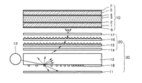
図1は、従来の液晶表示装置を示した断面図である。
図1を見れば、液晶表示装置は液晶パネル10及びバックライト装置30を含む。
液晶パネル10は、下部基板1、下部電極2、液晶層3、上部電極4及び上部基板5が順次積層されたものである。下部基板1の下方及び上部基板5の上方には偏光板6、7がさらに設けられる。液晶パネル10は、下部電極2及び上部電極4に印加される電気信号によって液晶層3の液晶分子の配向を変化させてバックライト装置30から入射する光を通過させるかまたは遮断することによって所望の画像を表示する。
FIG. 1 is a sectional view showing a conventional liquid crystal display device.
Referring to FIG. 1, the liquid crystal display includes a
The
バックライト装置30は液晶パネル10に光を供給する照明装置であって、導光板12、散乱パターン18、反射板11、及び光源13を含み、導光板12の上面には光学フィルム層20が積層される。光源13から放出された光は導光板12の側面に入射する。導光板12は屈折率が約1.5である光透過体であって、臨界角は約42°となる。したがって、導光板12に入射した光のうち、導光板12の上面に対する入射角が臨界角より小さな光は導光板12の上面を通じて放出され、残りの光は全反射されて導光板12全域に広がる。導光板12の下方には散乱パターン18が設けられる。散乱パターン18は光を散乱させるものであって、図1に図示されたように散乱された光のうち一部は導光板12の上面に向い、散乱パターン18を透過した光は反射板11により反射されて上方に向う。このうち、導光板12の上面に入射される入射角が臨界角より小さな光は透過され、そうでない光はまた全反射されて導光板12の内部に広がる。このように、透過、全反射及び散乱過程を反復することによってバックライト装置30は液晶パネル10に光を供給する面光源としての役割をする。
The
導光板12の上面を通過した光は光学フィルム層20を経て液晶パネル10に入射される。光学フィルム層20は拡散板14、プリズムシート15、16、保護膜17を含むことができる。拡散板14は光を拡散させて導光板12の上面に出る光の強度を均一にする。プリズムシート15、16は法線方向の輝度を向上させる。
前記のような液晶表示装置では、光源から放射された光が液晶パネルに到達するまで導光板と光学フィルム層など多数の光学的媒質を経つつ各媒質に吸収されて光損失が発生する。したがって、液晶パネルで所望の輝度を得るためには高出力光源を使用する必要がある。光出力が大きい光源は、普通、サイズが大きくて消費電力も大きく、さらに高コストである。導光板は普通厚さが約2〜3mmであるが、導光板を使用するバックライト装置としては液晶表示装置を薄型化するのに限界がある。
Light passing through the upper surface of the
In the above-described liquid crystal display device, light emitted from a light source is absorbed by each medium while passing through a plurality of optical media such as a light guide plate and an optical film layer until the light reaches a liquid crystal panel, thereby causing light loss. Therefore, it is necessary to use a high output light source in order to obtain a desired luminance in the liquid crystal panel. Light sources with high light output are typically large in size, consume large amounts of power, and are expensive. The light guide plate is usually about 2 to 3 mm in thickness, but there is a limit in reducing the thickness of the liquid crystal display device as a backlight device using the light guide plate.
本発明は前記問題点を解決するために創出されたものであって、光源と液晶パネル間の光学的媒質の数を減らすことによって薄型化、高輝度化、及び低コスト化を実現できるように改善された液晶表示装置を提供するところにその目的がある。 SUMMARY OF THE INVENTION The present invention has been made to solve the above problems, and is intended to realize a thinner, higher luminance, and lower cost by reducing the number of optical media between a light source and a liquid crystal panel. It is an object to provide an improved liquid crystal display.
前述した目的を達成するための本発明の液晶表示装置は、二基板間に封入された液晶層の配向を変化させることによって画像を表示する液晶表示装置において、側面に入射した光を上面に放出させる微細構造体を備える下部基板と、前記下部基板の側面に光を放射する光源と、前記下部基板の上面に設けられて一定の入射角度以上の光は反射し、残りの光は通過させる選択的反射板と、前記下部基板の下方に設けられる反射板とを含む。 The liquid crystal display device of the present invention for achieving the above-mentioned object emits light incident on a side surface to an upper surface in a liquid crystal display device that displays an image by changing the orientation of a liquid crystal layer sealed between two substrates. A lower substrate having a fine structure to be emitted, a light source emitting light to the side surface of the lower substrate, and a light provided on an upper surface of the lower substrate, reflecting light having a certain incident angle or more, and allowing the remaining light to pass. And a reflector provided below the lower substrate.
前記液晶表示装置は液晶層に入射する光を偏光させる偏光板をさらに具備し、前記偏光板は前記微細構造体と前記反射板間に位置し、前記選択的反射板の上方に位置する構成とすることもできる。
前記選択的反射板は光を偏光させる偏光機能をさらに行うように形成することができる。
The liquid crystal display device further includes a polarizing plate for polarizing light incident on a liquid crystal layer, wherein the polarizing plate is located between the microstructure and the reflector, and is located above the selective reflector. You can also.
The selective reflection plate may be formed to further perform a polarization function of polarizing light.
前記微細構造体は回折格子構造を有するホログラムパターンとすることが好ましい。前記ホログラムパターンは前記下部基板の下面と上面のうち少なくともいずれか一面に形成することが望ましく、前記ホログラムパターンの格子間隔は2μm以下であることが望ましい。
本発明の他の特徴による液晶表示装置は、二基板間に封入された液晶層の配向を変化させることによって画像を表示する液晶表示装置において、側面に入射した光を上面に放出させる微細構造体を備える下部基板と、前記下部基板の側面に光を放射する光源と、前記下部基板の上面に設けられるものであって、一定の入射角度以上の光は反射し、残りの光は通過させる選択的反射部及びあらゆる光を反射させる全反射部が備えられた光学板と、前記下部基板の下方に設けられる反射板とを含む。
The fine structure is preferably a hologram pattern having a diffraction grating structure. Preferably, the hologram pattern is formed on at least one of a lower surface and an upper surface of the lower substrate, and a lattice interval of the hologram pattern is preferably 2 μm or less.
A liquid crystal display device according to another aspect of the present invention is a liquid crystal display device that displays an image by changing the orientation of a liquid crystal layer sealed between two substrates, wherein a fine structure that emits light incident on a side surface to an upper surface is provided. A light source that emits light to the side surface of the lower substrate, and a light source that is provided on the upper surface of the lower substrate, wherein light having a certain incident angle or more is reflected and the remaining light is allowed to pass. An optical plate provided with a general reflection portion and a total reflection portion for reflecting all light; and a reflection plate provided below the lower substrate.
前記光学板は、各画素内に前記選択的反射部と前記全反射部とがそれぞれ少なくとも一つずつ位置するように形成されることが望ましい。
前記微細構造体は前記選択的反射部を通じて光を透過させうる位置にのみ選択的に形成することが好ましい。
The optical plate is preferably formed such that at least one of the selective reflection part and the total reflection part is located in each pixel.
Preferably, the fine structure is selectively formed only at a position where light can be transmitted through the selective reflection part.
本発明による液晶表示装置によれば、下部基板を導光板として使用することによって液晶表示装置の薄型化が可能であり、コストを節減できる。また光損失が減少し、同じ出力の光源を使用する場合にはさらに明るい液晶表示装置を具現できる。 According to the liquid crystal display device of the present invention, by using the lower substrate as a light guide plate, the thickness of the liquid crystal display device can be reduced, and the cost can be reduced. In addition, light loss is reduced, and a brighter liquid crystal display device can be realized when a light source having the same output is used.
以下添付した図面を参照しながら本発明の望ましい実施例を詳細に説明する。
図2は本発明による液晶表示装置の一実施例を示した断面図である。
図2には、上部基板102、上部電極103、液晶層104、下部電極105、下部基板110が図示されている。液晶層104の液晶分子は配向膜(図示せず)により一定の方向に配向処理されている。下部基板110及び上部基板102は光透過体であって普通ガラスより製作される。上部電極103及び下部電極105は透明な導電膜であって、印加される電気信号によって液晶層103の配向を変化させる。上部基板102の上方には偏光板101が備えられる。
Hereinafter, preferred embodiments of the present invention will be described in detail with reference to the accompanying drawings.
FIG. 2 is a sectional view showing an embodiment of the liquid crystal display device according to the present invention.
FIG. 2 illustrates an
下部基板110の側面112には光源160が設置される。光源160はLED(light emitting diode)のような点光源とすることができ、冷陰極蛍光ランプ(CCFL:cold cathode fluorescent lamp)のような線光源とすることもできる。光源160は多数設置することも可能である。また、下部基板110の一側面だけでなく他の側面にも設置することができる。
The
下部基板110には光源160から入射して下部基板110の内部を進む光を上方に放出する微細構造体が設けられる。微細構造体は散乱パターンまたは回折格子構造を有するホログラムパターンとすることができる。ホログラムパターンは格子間隔が2μm以下であることが回折効率面で望ましい。本実施例では微細構造体として格子間隔0.4μm、格子深さ0.2μmのホログラムパターン120を形成する。ホログラムパターン120は下部基板110の底面113及び/または上面114に設けられる。
The
ホログラムパターン120の下方には反射板140が設けられる。反射板140はホログラムパターン120により回折されて下方に進んだ光を上方に反射させる。
本発明による液晶表示装置は下部基板110が導光板の役割を兼ねることを特徴とする。従来の液晶表示装置では、下部基板の上面に下部基板と屈折率がほぼ同じである下部電極が積層されるために、下部基板と下部電極間の境界面で全反射が起きる臨界角はほぼ90°となる。したがって、下部基板の側面を通じて入射した光が下部基板と下部電極間の境界面で全反射をほとんど起こさないために、下部基板が導光板の役割を行えない。
A
The liquid crystal display according to the present invention is characterized in that the
本実施例では下部基板110を導光板として使用するためにその上面114に選択的反射板130が設けられる。選択的反射板130は、下部基板110の上面114に入射する光のうち入射角Aが一定の角度を超える光は反射し、残りの光は通過させる。たとえば、下部基板110が約42°の臨界角を有するPMMA導光板のような役割を行うためには、選択的反射板130は入射角Aが約42°を超える光は反射し、それ以下の入射角Aを有する光は通過させるように形成すればよい。選択的反射板130がいかなる角度範囲の光を通過させるかは液晶表示装置の輝度及び輝度均一度を考慮して適切に選択できる。また、下部基板110から出る光はなるべく上面114に対して垂直に近いものが望ましいために、選択的反射板130は入射角Aが30°以内、言い換えれば下部基板110の上面と60°以上の角をなす光だけを透過させるように形成することができる。
In this embodiment, a selective reflection plate 130 is provided on the
ホログラムパターン120と反射板140間には偏光板150が設けられる。偏光板150は偏光板101と偏光方向が同じかまたは異なる。これは液晶層104の配向方向と、電極103、105に電流が印加された時に光を通過させるかまたはその反対にするかによって決定される。光は液晶層104に入射する前に一定の方向に偏光されればよい。したがって、偏光板150は選択的反射板130の上方に設置してもよい。
A
さらに、このような構成による作用効果を説明する。
光源から放射した光は下部基板110の側面112を通じて下部基板110に入射する。下部基板110の内部から上面114に向う光はその入射角Aが一定の角度以下であれば選択的反射板130を透過して上方に放出される。残りの光は反射されて再び下部基板110の内部に進む。このように、選択的反射板130により光は下部基板110の全領域に伝えられて導光板の役割を行う。
Further, the operation and effect of such a configuration will be described.
Light emitted from the light source enters the
ホログラムパターン120に入射した光は回折されて反射板140側に進み、一部は反射されて下部基板110内部に広がる。回折されてホログラムパターン120を透過した光は偏光板150を通過しながら偏光され、反射板140で反射されて再び上方に進む。この光が選択的反射板130に入射した場合、前記のように入射角Aが一定の角度以上になれば再び反射され、それ以下の入射角Aを有する光は選択的反射板130を透過して液晶層104側に入射する。
The light incident on the
下部電極105及び上部電極103には表示しようとする画像によって液晶層104内部の液晶分子が適切な方向に配向されるように電気信号が印加される。液晶分子はその配向方向によって上部基板102側に光を通過させるか、または遮断する。これにより液晶表示装置には所望の画像が表示される。
結局、下部基板110は光源160、選択的反射板130及び微細構造体と共にバックライト装置を形成する。
An electric signal is applied to the
After all, the
このように、本実施例による液晶表示装置は下部基板が導光板の役割を行うために従来の液晶表示装置のような導光板を必要としない。したがって、従来の液晶表示装置に比べて薄型化された液晶表示装置の具現が可能である。また、コストも節減できる。また、光源から液晶層に至る過程で少なくとも導光板という光学的媒質を省略することによって光損失を減らすことができ、光利用効率を向上させうる。また、バックライト装置の機能を行う各種構成要素、例えば選択的反射板、微細構造体などが下部基板を中心に設けられるために、液晶表示装置の製造工程において下部基板を中心にあらゆる工程を進めることができる。 As described above, the liquid crystal display according to the present embodiment does not require a light guide plate unlike the conventional liquid crystal display device because the lower substrate functions as a light guide plate. Therefore, it is possible to realize a liquid crystal display device that is thinner than a conventional liquid crystal display device. Also, costs can be saved. Further, by omitting at least an optical medium called a light guide plate in the process from the light source to the liquid crystal layer, light loss can be reduced and light use efficiency can be improved. In addition, since various components for performing the function of the backlight device, such as a selective reflection plate and a microstructure, are provided around the lower substrate, all processes are performed around the lower substrate in the manufacturing process of the liquid crystal display device. be able to.
図2に図示された実施例では偏光板150が別途に設けられている。しかし、選択的反射板130が偏光板の役割を行えるように形成することもできる。この場合、偏光板を別途設ける必要がなくなる。
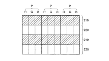
図3は、本発明による液晶表示装置の他の実施例を示したものであり、図4は光学板200の形成例を示した平面図である。
In the embodiment shown in FIG. 2, a
FIG. 3 shows another embodiment of the liquid crystal display device according to the present invention, and FIG. 4 is a plan view showing an example of forming an
図3を見れば、図2に図示された構成とほぼ同一であるが、半透過型液晶表示装置を具現するために下部基板110の上面114に選択的反射板130の代りに光学板200が形成されている。
図4に示されるように、光学板200は、下部基板110の上面114を一画素Pずつ区分して各画素P毎に一定の入射角度以上の光は反射し、残りの光は通過させる選択的反射部210及びあらゆる光を反射させる全反射部220を形成したものである。一つの画素P内に選択的反射部210と全反射部220とは少なくとも一つずつ形成されることが望ましい。カラー液晶表示装置の場合、一つの画素PはR(red)、G(green)、B(blue)3つの画素よりなる。
Referring to FIG. 3, the structure is almost the same as the structure shown in FIG. 2, but an
As shown in FIG. 4, the
選択的反射部210は前述した図2の選択的反射板130のような役割を行う。全反射部220は外部から上部基板105を通じて入る光と、光源160から放射されて下部基板110の内部に進む光とをいずれも反射する。
このような構成による作用効果を説明する。
光源160から放射された光は側面112を通じて下部基板110に入射する。下部基板110内で光は選択的反射部210、全反射部220、及びホログラムパターン120に入射する。ホログラムパターン120に入射した光は、一部は反射されて下部基板110の他の領域に進み、一部は回折されて反射板140に進む。この時、偏光板150を通過しながら一方向に偏光される。反射板140で反射した光は上方に進んで全反射部220または選択的反射部210に入射する。選択的反射部210に入射した光のうち入射角Aが一定の入射角度を超える光及び全反射部220に入射した光は反射されて下部基板110の全領域に均一に伝えられる。光源160からホログラムパターン120を経ずに直ちに光学板200に入射した光も前記のような過程を経て下部基板110の内部に均一に伝えられる。選択的反射部210に入射した光のうち入射角Aが一定の角度以内である光は透過されて上方に出光される。
The
The operation and effect of such a configuration will be described.
Light emitted from the
外部から入射した光は全反射部210で反射されて直ちに液晶層104側に進むか、または選択的反射部210を通じて下部基板110に入射する。
このような構成による液晶表示装置は図2に示された実施例の効果に加えて次のような効果を有する。本実施例による液晶表示装置は2つのモードで動作される。すなわち、液晶表示装置を使用する空間が明るい空間である場合には外部光を使用できるために光源160の出力を減らして消費電力を減らすことができ、暗い空間で使用する場合には外部光源を使用できないために光源160から放射された光を使用する。
Light incident from the outside is reflected by the
The liquid crystal display device having such a configuration has the following effects in addition to the effects of the embodiment shown in FIG. The liquid crystal display according to the present embodiment operates in two modes. That is, when the space where the liquid crystal display device is used is a bright space, external light can be used, so that the output of the
図5は、本発明による液晶表示装置のまた他の実施例を示した断面図である。
図5を見れば、図4に図示された構成とほぼ同一であるが、ホログラムパターン120が下部基板110の底面113全体にわたって形成されず、ホログラムパターン120により回折された光が選択的反射部210を通過できる領域のみに形成される。
図4に示されたように、底面113の全面にわたってホログラムパターン120を形成する場合には、ホログラムパターン120により回折されて上方に進む光のうち全反射部220に進んだ光は反射されて下部基板110に広がりながら再びホログラムパターン120に入射する過程を反復する。しかし、本実施例に選択的反射部210を通過できる領域のみにホログラムパターン120を形成すれば、下部基板110を離脱するまでの光路が短くなって光路中の媒質に吸収されて損失する光量が減る。したがって、光利用効率が向上する。すなわち、同じ出力の光源を使用してもさらに明るい液晶表示装置が具現できる。
FIG. 5 is a sectional view showing another embodiment of the liquid crystal display device according to the present invention.
Referring to FIG. 5, the configuration is substantially the same as that shown in FIG. 4, but the
As shown in FIG. 4, when the
本発明は前記に説明され図面に例示されたものにより限定されず、特許請求の範囲内でさらに多くの変形及び変容例が可能である。 The invention is not limited to what has been described and illustrated in the drawings, and many more modifications and variations are possible within the scope of the appended claims.
本発明は電気信号により液晶層の液晶分子の配向を変化させて光源からの光を通過させるかまたは遮断することによって所望の画像を表示する液晶表示装置に適用される。 The present invention is applied to a liquid crystal display device that displays a desired image by changing the orientation of liquid crystal molecules in a liquid crystal layer by an electric signal and passing or blocking light from a light source.
101 偏光板
102 上部基板
103 上部電極
104 液晶層
105 下部電極
110 下部基板
112 下部基板の側面
113 下部基板の底面
114 下部基板の上面
120 ホログラムパターン
130 選択的反射板
140 反射板
150 偏光板
160 光源
101
Claims (17)
側面に入射する光を上面に放出させる微細構造体を備える下部基板と、
前記下部基板の側面に光を放射する光源と、
前記下部基板の上面に設けられて一定の入射角度以上の光は反射し、残りの光は通過させる選択的反射板と、
前記下部基板の下方に設けられる反射板と、
を含む液晶表示装置。 In a liquid crystal display device that displays an image by changing the orientation of a liquid crystal layer sealed between two substrates,
A lower substrate having a microstructure for emitting light incident on the side surface to the upper surface,
A light source that emits light to the side surface of the lower substrate,
A selective reflection plate provided on the upper surface of the lower substrate and reflecting light having a certain incident angle or more and allowing the remaining light to pass therethrough,
A reflector provided below the lower substrate,
Liquid crystal display device including.
側面に入射する光を上面に放出させる微細構造体を備える下部基板と、
前記下部基板の側面に光を放射する光源と、
前記下部基板の上面に設けられるものであって、一定の入射角度以上の光は反射させ、残りの光は通過させる選択的反射部及びあらゆる光を反射させる全反射部を備える光学板と、
前記下部基板の下方に設けられる反射板と、
を含む液晶表示装置。 In a liquid crystal display device that displays an image by changing the orientation of a liquid crystal layer sealed between two substrates,
A lower substrate having a microstructure for emitting light incident on the side surface to the upper surface,
A light source that emits light to the side surface of the lower substrate,
An optical plate, which is provided on the upper surface of the lower substrate, reflects light having a certain incident angle or more, and includes a selective reflection portion that transmits the remaining light and a total reflection portion that reflects all light,
A reflector provided below the lower substrate,
Liquid crystal display device including.
16. The liquid crystal display device according to claim 15, wherein a lattice interval of the hologram pattern is 2 [mu] m or less.
Applications Claiming Priority (1)
| Application Number | Priority Date | Filing Date | Title |
|---|---|---|---|
| KR10-2003-0002381A KR100506088B1 (en) | 2003-01-14 | 2003-01-14 | Liquid crystal displaying apparatus |
Publications (1)
| Publication Number | Publication Date |
|---|---|
| JP2004220031A true JP2004220031A (en) | 2004-08-05 |
Family
ID=32588951
Family Applications (1)
| Application Number | Title | Priority Date | Filing Date |
|---|---|---|---|
| JP2004006764A Pending JP2004220031A (en) | 2003-01-14 | 2004-01-14 | Liquid crystal display device |
Country Status (9)
| Country | Link |
|---|---|
| US (2) | US7221418B2 (en) |
| EP (1) | EP1439409B1 (en) |
| JP (1) | JP2004220031A (en) |
| KR (1) | KR100506088B1 (en) |
| CN (1) | CN1279394C (en) |
| AT (1) | ATE345517T1 (en) |
| DE (1) | DE60309660T2 (en) |
| DK (1) | DK1439409T3 (en) |
| ES (1) | ES2275971T3 (en) |
Cited By (2)
| Publication number | Priority date | Publication date | Assignee | Title |
|---|---|---|---|---|
| JP2008102416A (en) * | 2006-10-20 | 2008-05-01 | Hitachi Displays Ltd | Wire grid polarizer and liquid crystal display using the same |
| KR20210101301A (en) * | 2018-12-18 | 2021-08-18 | 비보 모바일 커뮤니케이션 컴퍼니 리미티드 | Pressure measuring devices, screen assemblies and mobile terminals |
Families Citing this family (31)
| Publication number | Priority date | Publication date | Assignee | Title |
|---|---|---|---|---|
| TWI289708B (en) | 2002-12-25 | 2007-11-11 | Qualcomm Mems Technologies Inc | Optical interference type color display |
| US7342705B2 (en) | 2004-02-03 | 2008-03-11 | Idc, Llc | Spatial light modulator with integrated optical compensation structure |
| US7813026B2 (en) * | 2004-09-27 | 2010-10-12 | Qualcomm Mems Technologies, Inc. | System and method of reducing color shift in a display |
| US7630123B2 (en) * | 2004-09-27 | 2009-12-08 | Qualcomm Mems Technologies, Inc. | Method and device for compensating for color shift as a function of angle of view |
| US7508571B2 (en) * | 2004-09-27 | 2009-03-24 | Idc, Llc | Optical films for controlling angular characteristics of displays |
| US7845841B2 (en) * | 2006-08-28 | 2010-12-07 | Qualcomm Mems Technologies, Inc. | Angle sweeping holographic illuminator |
| WO2008036958A2 (en) | 2006-09-23 | 2008-03-27 | Ylx Corporation | Brightness enhancement method and apparatus of light emitting diodes |
| EP2069838A2 (en) | 2006-10-06 | 2009-06-17 | Qualcomm Mems Technologies, Inc. | Illumination device with built-in light coupler |
| US7855827B2 (en) | 2006-10-06 | 2010-12-21 | Qualcomm Mems Technologies, Inc. | Internal optical isolation structure for integrated front or back lighting |
| US8107155B2 (en) | 2006-10-06 | 2012-01-31 | Qualcomm Mems Technologies, Inc. | System and method for reducing visual artifacts in displays |
| US8872085B2 (en) | 2006-10-06 | 2014-10-28 | Qualcomm Mems Technologies, Inc. | Display device having front illuminator with turning features |
| JP2010510530A (en) | 2006-10-06 | 2010-04-02 | クォルコム・メムズ・テクノロジーズ・インコーポレーテッド | Optical loss structure integrated into lighting equipment |
| EP1946162A2 (en) | 2006-10-10 | 2008-07-23 | Qualcomm Mems Technologies, Inc | Display device with diffractive optics |
| US7864395B2 (en) | 2006-10-27 | 2011-01-04 | Qualcomm Mems Technologies, Inc. | Light guide including optical scattering elements and a method of manufacture |
| JP2009009116A (en) * | 2007-06-01 | 2009-01-15 | Citizen Holdings Co Ltd | Liquid crystal display device |
| EP2158518B1 (en) | 2007-06-14 | 2015-01-14 | Nokia Corporation | Displays with integrated backlighting |
| US8068710B2 (en) | 2007-12-07 | 2011-11-29 | Qualcomm Mems Technologies, Inc. | Decoupled holographic film and diffuser |
| JP2011515017A (en) * | 2008-02-12 | 2011-05-12 | クォルコム・メムズ・テクノロジーズ・インコーポレーテッド | Two-layer thin film holographic solar collector and solar concentrator |
| US8654061B2 (en) | 2008-02-12 | 2014-02-18 | Qualcomm Mems Technologies, Inc. | Integrated front light solution |
| WO2009102731A2 (en) | 2008-02-12 | 2009-08-20 | Qualcomm Mems Technologies, Inc. | Devices and methods for enhancing brightness of displays using angle conversion layers |
| WO2009129264A1 (en) | 2008-04-15 | 2009-10-22 | Qualcomm Mems Technologies, Inc. | Light with bi-directional propagation |
| KR101469474B1 (en) * | 2008-04-30 | 2014-12-12 | 엘지디스플레이 주식회사 | Display device |
| JP2012503221A (en) * | 2008-09-18 | 2012-02-02 | クォルコム・メムズ・テクノロジーズ・インコーポレーテッド | Increasing the angular range of light collection in solar collectors / collectors |
| KR20100043972A (en) * | 2008-10-21 | 2010-04-29 | 삼성전자주식회사 | Optical signal concentrator and optcial receiver using the same |
| WO2010138762A1 (en) * | 2009-05-29 | 2010-12-02 | Qualcomm Mems Technologies, Inc. | Illumination devices for reflective displays |
| US8902484B2 (en) | 2010-12-15 | 2014-12-02 | Qualcomm Mems Technologies, Inc. | Holographic brightness enhancement film |
| JP6550143B2 (en) * | 2015-03-16 | 2019-07-24 | レイア、インコーポレイテッドLeia Inc. | Unidirectional grating-based backlighting using an angle selective reflective layer |
| CN106292052B (en) * | 2016-10-24 | 2019-04-09 | 京东方科技集团股份有限公司 | A kind of display panel and device |
| CN109239965B (en) * | 2018-09-30 | 2021-11-23 | 京东方科技集团股份有限公司 | Display device and control method thereof |
| WO2020186492A1 (en) * | 2019-03-21 | 2020-09-24 | 京东方科技集团股份有限公司 | Display panel |
| CN112180601B (en) * | 2020-09-30 | 2022-05-31 | 厦门天马微电子有限公司 | Display module assembly and car |
Family Cites Families (16)
| Publication number | Priority date | Publication date | Assignee | Title |
|---|---|---|---|---|
| JP2823470B2 (en) * | 1993-03-09 | 1998-11-11 | シャープ株式会社 | Optical scanning device, display device using the same, and image information input / output device |
| JP3195221B2 (en) * | 1995-10-30 | 2001-08-06 | シャープ株式会社 | Liquid crystal display |
| JPH10111502A (en) * | 1996-10-04 | 1998-04-28 | Sony Corp | Reflection type guest-host liquid crystal display device |
| WO1998052094A1 (en) * | 1997-05-14 | 1998-11-19 | Seiko Epson Corporation | Display and electronic device comprising the same |
| JPH11232919A (en) * | 1998-02-17 | 1999-08-27 | Fuji Xerox Co Ltd | Front light lighting system and reflecting type display device |
| JP2986773B2 (en) * | 1998-04-01 | 1999-12-06 | 嶋田プレシジョン株式会社 | Light guide plate for point light source |
| JP3564358B2 (en) * | 1999-03-29 | 2004-09-08 | シャープ株式会社 | Liquid crystal display |
| JP2000330098A (en) * | 1999-05-24 | 2000-11-30 | Nitto Denko Corp | Substrate for liquid crystal cell, liquid crystal cell and liquid crystal display device |
| TWI235270B (en) * | 1999-07-02 | 2005-07-01 | Keun-Chang Yang | Plane light source unit and method for manufacturing holographic light-guide plate used for flat panel display |
| US6429913B2 (en) * | 1999-12-23 | 2002-08-06 | Neurok, Llc | System and method for the manufacture of a universal reflective-transmissive display |
| JP2002006135A (en) * | 2000-06-20 | 2002-01-09 | Minolta Co Ltd | Polarized light separating element, and lighting optical system |
| JP4439084B2 (en) * | 2000-06-14 | 2010-03-24 | 日東電工株式会社 | Liquid crystal display |
| EP1197789A1 (en) * | 2000-10-17 | 2002-04-17 | Telefonaktiebolaget L M Ericsson (Publ) | Edge-illuminated liquid-crystal display |
| JP4119085B2 (en) | 2000-12-20 | 2008-07-16 | 東芝松下ディスプレイテクノロジー株式会社 | Liquid crystal display device and stereoscopic display device |
| JP3598987B2 (en) * | 2001-03-28 | 2004-12-08 | セイコーエプソン株式会社 | Liquid crystal display and electronic equipment |
| KR20030029251A (en) * | 2001-10-05 | 2003-04-14 | 삼성전자주식회사 | Liquid crystal display device |
-
2003
- 2003-01-14 KR KR10-2003-0002381A patent/KR100506088B1/en active IP Right Grant
- 2003-06-04 AT AT03012718T patent/ATE345517T1/en active
- 2003-06-04 ES ES03012718T patent/ES2275971T3/en not_active Expired - Lifetime
- 2003-06-04 DE DE60309660T patent/DE60309660T2/en not_active Expired - Lifetime
- 2003-06-04 DK DK03012718T patent/DK1439409T3/en active
- 2003-06-04 EP EP03012718A patent/EP1439409B1/en not_active Expired - Lifetime
- 2003-06-13 CN CNB031423485A patent/CN1279394C/en not_active Expired - Fee Related
- 2003-07-23 US US10/624,541 patent/US7221418B2/en not_active Expired - Lifetime
-
2004
- 2004-01-14 JP JP2004006764A patent/JP2004220031A/en active Pending
-
2007
- 2007-04-02 US US11/730,451 patent/US20070177076A1/en not_active Abandoned
Cited By (8)
| Publication number | Priority date | Publication date | Assignee | Title |
|---|---|---|---|---|
| JP2008102416A (en) * | 2006-10-20 | 2008-05-01 | Hitachi Displays Ltd | Wire grid polarizer and liquid crystal display using the same |
| US8049841B2 (en) | 2006-10-20 | 2011-11-01 | Hitachi Displays, Ltd. | Wire grid polarized and liquid crystal display device using the same |
| US8199282B2 (en) | 2006-10-20 | 2012-06-12 | Hitachi Displays, Ltd. | Wire grid polarized and liquid crystal display device using the same |
| KR20210101301A (en) * | 2018-12-18 | 2021-08-18 | 비보 모바일 커뮤니케이션 컴퍼니 리미티드 | Pressure measuring devices, screen assemblies and mobile terminals |
| JP2022515091A (en) * | 2018-12-18 | 2022-02-17 | 維沃移動通信有限公司 | Pressure detectors, screen components and mobile terminals |
| JP7258148B2 (en) | 2018-12-18 | 2023-04-14 | 維沃移動通信有限公司 | Pressure sensing devices, screen components and mobile terminals |
| KR102552626B1 (en) * | 2018-12-18 | 2023-07-05 | 비보 모바일 커뮤니케이션 컴퍼니 리미티드 | Pressure sensing devices, screen assemblies and mobile terminals |
| US11720209B2 (en) | 2018-12-18 | 2023-08-08 | Vivo Mobile Communication Co., Ltd. | Pressure detection apparatus, screen assembly, and mobile terminal |
Also Published As
| Publication number | Publication date |
|---|---|
| US7221418B2 (en) | 2007-05-22 |
| DE60309660D1 (en) | 2006-12-28 |
| CN1517761A (en) | 2004-08-04 |
| DK1439409T3 (en) | 2007-01-08 |
| KR20040065416A (en) | 2004-07-22 |
| KR100506088B1 (en) | 2005-08-03 |
| ATE345517T1 (en) | 2006-12-15 |
| US20070177076A1 (en) | 2007-08-02 |
| US20040135942A1 (en) | 2004-07-15 |
| CN1279394C (en) | 2006-10-11 |
| EP1439409B1 (en) | 2006-11-15 |
| EP1439409A1 (en) | 2004-07-21 |
| DE60309660T2 (en) | 2007-03-08 |
| ES2275971T3 (en) | 2007-06-16 |
Similar Documents
| Publication | Publication Date | Title |
|---|---|---|
| JP2004220031A (en) | Liquid crystal display device | |
| JP4153776B2 (en) | Planar light source device and liquid crystal display device using the same | |
| JP2004061693A (en) | Surface light source device and liquid crystal display device using same | |
| JP2007066555A (en) | Surface light source and liquid crystal display device | |
| JP2006209131A (en) | Integrated liquid crystal display | |
| KR102090457B1 (en) | Liquid crystal display device | |
| EP2450742B1 (en) | Backlight source and thinning method for the same and liquid crystal device with the same | |
| KR101085444B1 (en) | Optical member and back light assembly having the light guide plate, and display device having the back light assembly | |
| JP5339773B2 (en) | Liquid crystal display | |
| KR101792102B1 (en) | Liquid crystal display device | |
| KR20110073725A (en) | Liquid crystal display device | |
| JP2007065611A (en) | Prism sheet and backlight unit having same prism sheet and employed in liquid crystal display panel | |
| WO2006104159A1 (en) | Display unit | |
| JP2007004162A (en) | Display panel assembly and display apparatus having the same | |
| KR20060001251A (en) | Back light unit | |
| JP2006323221A (en) | Liquid crystal display apparatus | |
| KR20060131243A (en) | Back light assembly and display apparatus having the same | |
| JP2000075292A (en) | Reflective display device | |
| JP2011108367A (en) | Planar light source device, and display device | |
| JP2011191387A (en) | Liquid crystal display device | |
| KR101774572B1 (en) | Display device | |
| KR100608890B1 (en) | Liquid Crystal Display Panel And Liquid Crystal Display Device Including the same | |
| KR100939192B1 (en) | Optical panel for backlight by distributing delicate optical waveguides | |
| KR102262569B1 (en) | Backlight Unit and Liquid Crystal Display Device having the same | |
| JPH11109342A (en) | Liquid crystal display device |
Legal Events
| Date | Code | Title | Description |
|---|---|---|---|
| A977 | Report on retrieval |
Free format text: JAPANESE INTERMEDIATE CODE: A971007 Effective date: 20050909 |
|
| A131 | Notification of reasons for refusal |
Free format text: JAPANESE INTERMEDIATE CODE: A131 Effective date: 20051004 |
|
| A521 | Request for written amendment filed |
Free format text: JAPANESE INTERMEDIATE CODE: A523 Effective date: 20051226 |
|
| A131 | Notification of reasons for refusal |
Free format text: JAPANESE INTERMEDIATE CODE: A131 Effective date: 20060207 |
|
| A601 | Written request for extension of time |
Free format text: JAPANESE INTERMEDIATE CODE: A601 Effective date: 20060502 |
|
| A602 | Written permission of extension of time |
Free format text: JAPANESE INTERMEDIATE CODE: A602 Effective date: 20060510 |
|
| A02 | Decision of refusal |
Free format text: JAPANESE INTERMEDIATE CODE: A02 Effective date: 20061010 |