JP2004200646A - Plasma processing system and plasma processing method - Google Patents
Plasma processing system and plasma processing method Download PDFInfo
- Publication number
- JP2004200646A JP2004200646A JP2003270987A JP2003270987A JP2004200646A JP 2004200646 A JP2004200646 A JP 2004200646A JP 2003270987 A JP2003270987 A JP 2003270987A JP 2003270987 A JP2003270987 A JP 2003270987A JP 2004200646 A JP2004200646 A JP 2004200646A
- Authority
- JP
- Japan
- Prior art keywords
- electromagnetic wave
- plasma processing
- waveguide
- processing apparatus
- plasma
- Prior art date
- Legal status (The legal status is an assumption and is not a legal conclusion. Google has not performed a legal analysis and makes no representation as to the accuracy of the status listed.)
- Pending
Links
Images


Abstract
Description
本発明は、プラズマ処理装置およびプラズマ処理方法に係り、特に、大型の角型基板に対して、膜堆積、表面改質、あるいはエッチング等のプラズマ処理を施すためのプラズマ処理装置およびプラズマ処理方法に関する。 The present invention relates to a plasma processing apparatus and a plasma processing method, and more particularly to a plasma processing apparatus and a plasma processing method for performing plasma processing such as film deposition, surface modification, or etching on a large square substrate. .
従来、半導体装置や液晶表示装置等の製造プロセスにおいて、膜堆積、表面改質、あるいはエッチング等のプラズマ処理を施すためには、平行平板型の高周波プラズマ処理装置や、電子サイクロトロン共鳴(ECR)プラズマ処理装置などが用いられている。
しかしながら、平行平板型プラズマ処理装置では、プラズマ密度が低く、電子温度が高い、また、ECRプラズマ処理装置では、プラズマ励起に直流磁場が必要であるため、大面積の処理が困難であるという問題を抱えている。
これに対して、近年、プラズマ励起に磁場が不要であり、高密度でかつ電子温度が低いプラズマが生成し得るプラズマ処理装置が提案されている。
以下、そのような装置について説明する。
2. Description of the Related Art Conventionally, in a manufacturing process of a semiconductor device, a liquid crystal display device, or the like, in order to perform plasma processing such as film deposition, surface modification, or etching, a parallel plate type high frequency plasma processing apparatus or an electron cyclotron resonance (ECR) plasma is used. Processing devices and the like are used.
However, the parallel plate type plasma processing apparatus has a problem in that the plasma density is low and the electron temperature is high, and the ECR plasma processing apparatus requires a DC magnetic field for plasma excitation, which makes it difficult to process a large area. Have
On the other hand, in recent years, there has been proposed a plasma processing apparatus which does not require a magnetic field for plasma excitation and can generate plasma with high density and low electron temperature.
Hereinafter, such an apparatus will be described.
《第1の従来装置》
図15(a)は、従来の第1のプラズマ処理装置の上面図、(b)は断面図である。
この装置は、下記特許文献1に記載されている。
71は同軸伝送路、73は円形マイクロ波放射板、72は円形マイクロ波放射板73に同心円状に設けたスロット、74は誘電体からなる電磁波放射窓、75は真空容器、76はガス導入口、77はガス排気口、78はプラズマ処理する基板、79は基板支持台である。
この装置は、同心円状に配されたスロット72を有する円形マイクロ波放射板73に、同軸伝送路71からマイクロ波電力が供給される。
この装置では、同軸伝送路71から円形マイクロ波放射板73の中心に向けて導入したマイクロ波を、円形マイクロ波放射板73の径方向に伝播させつつ、円形マイクロ波放射板73に設けたスロット72から放射することにより、真空容器75内に均一なプラズマを生成しようとするものである。
<< First conventional device >>
FIG. 15A is a top view of a first conventional plasma processing apparatus, and FIG. 15B is a cross-sectional view.
This device is described in
71 is a coaxial transmission line, 73 is a circular microwave radiating plate, 72 is a slot provided concentrically on the circular
In this device, microwave power is supplied from a
In this device, while the microwave introduced from the
《第2の従来装置》
図16(a)は、従来の第2のプラズマ処理装置の上面図、(b)は断面図である。
この装置は、下記特許文献2に記載されている。
81は矩形導波管、82は導波管アンテナを構成するスロット、83はマイクロ波源、84は誘電体からなる電磁波放射窓、85は真空容器、86はガス導入口、87はガス排気口、88はプラズマ処理する基板、89は基板支持台、110は矩形導波管81の反射面(短絡面、R面)、111は矩形導波管81のH面(マイクロ波の電界方向に垂直な面)である。
この装置は、矩形導波管81のH面111の一部に配され、導波管アンテナを構成するスロット82から、電磁波放射窓84を介してマイクロ波電力を供給することにより、真空容器85内にプラズマを生成する。
この装置では、矩形導波管81の反射面110でのマイクロ波の反射を考慮し、矩形導波管81のH面111に設けた2つのスロット82の幅(開口面積)を変化させることにより(図示は省略)、マイクロ波のスロット82からの放射電力を均一化しようとするものである。なお、図16(a)では、スロット82の幅の変化については、図示省略しているが、当該公報に記載されているように、例えば、スロット82は、矩形導波管81の反射面110に向かって狭くなるように、階段状あるいはテーパ状に変化した形状を有する。
これにより、生成されたプラズマが十分に拡散すれば、2つのスロット82から放射されたマイクロ波電力により比較的均一なプラズマを発生させることが可能となる。
なお、最近では、半導体装置や液晶表示装置を製造するために用いるプラズマ処理装置においては、基板サイズの拡大に伴って、装置の大型化が進み、特に液晶表示装置の場合には、1メートル級の基板を処理するための装置が必要である。これは半導体装置の製造に用いる直径300mmの基板の約10倍の面積に当たる。
さらに、上記プラズマ処理には、モノシランガス、酸素ガス、水素ガス、塩素ガスという反応性ガスが原料ガスとして利用されている。これらのガスのプラズマ中には、多くの負イオン(O−、H−、Cl−等)が存在しており、これらの振る舞いを考慮に入れた製造設備および製造方法が求められている。
<< 2nd conventional device >>
FIG. 16A is a top view of a second conventional plasma processing apparatus, and FIG. 16B is a cross-sectional view.
This device is described in
81 is a rectangular waveguide, 82 is a slot constituting a waveguide antenna, 83 is a microwave source, 84 is an electromagnetic wave radiation window made of a dielectric, 85 is a vacuum vessel, 86 is a gas inlet, 87 is a gas exhaust, 88 is a substrate to be subjected to plasma processing, 89 is a substrate support, 110 is a reflection surface (short-circuit surface, R surface) of the
This device is provided on a part of the
In this device, the width (opening area) of the two
Accordingly, if the generated plasma is sufficiently diffused, it is possible to generate a relatively uniform plasma by the microwave power radiated from the two
In recent years, in a plasma processing apparatus used for manufacturing a semiconductor device or a liquid crystal display device, the size of the device has been increasing with the increase in the substrate size. An apparatus for processing the substrate is required. This is about 10 times the area of a substrate having a diameter of 300 mm used for manufacturing a semiconductor device.
Further, in the plasma treatment, a reactive gas such as a monosilane gas, an oxygen gas, a hydrogen gas, and a chlorine gas is used as a source gas. Many negative ions (O − , H − , Cl −, etc.) are present in the plasma of these gases, and a manufacturing facility and a manufacturing method that take these behaviors into consideration are required.
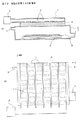
《第3の従来装置》
図17(a)は、第3のプラズマ処理装置の断面図、(b)は上面図である。
この従来装置は、下記特許文献3に記載されている。
101は矩形導波管、102は導波管アンテナを構成する結合孔、104は誘電体からなる電磁波放射窓、105は真空容器である。なお、プラズマ処理する基板や基板支持台等は図示省略している。
この装置は、3列の矩形導波管101を並べた表面波プラズマ処理装置であり、真空容器105に複数の矩形導波管101を等間隔に平行に配設し、各矩形導波管101にはその先端側に向かって結合係数を順次大きくした結合孔102を設け、真空容器105には各結合孔102に対応して分割形成した電磁波放射窓104が設けられている。
<< 3rd conventional device >>
FIG. 17A is a cross-sectional view of the third plasma processing apparatus, and FIG. 17B is a top view.
This conventional device is described in
101 is a rectangular waveguide, 102 is a coupling hole forming a waveguide antenna, 104 is an electromagnetic radiation window made of a dielectric, and 105 is a vacuum vessel. Note that a substrate to be subjected to plasma processing, a substrate support, and the like are not shown.
This apparatus is a surface wave plasma processing apparatus in which three rows of
《第4の従来装置》
図18は、第4のプラズマ処理装置の切断上面図である。
この従来装置は、下記特許文献4に記載されている。
マイクロ波電源1026から導波管1023を通って、導入部1311から誘電体電路1031にマイクロ波が導入される。マイクロ波は、整合部1312から仕切り板1314と矩形部1313から形成される導波管相当部分を通り、マイクロ波導入口1003から、反応室に導かれる。なお、1004はマイクロ波導入窓である。
<< 4th conventional device >>
FIG. 18 is a cut-away top view of the fourth plasma processing apparatus.
This conventional device is described in
Microwaves are introduced from the microwave power supply 1026 through the
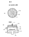
《第5の従来装置》
図19は、第5のプラズマ処理装置の切断上面図である。
この従来装置は、下記特許文献5に記載されている。
マイクロ波電源1126から供給されたマイクロ波が、マイクロ波分配器1027を通って、導波管1028に分配される。なお、1002は反応室である。
<< 5th conventional device >>
FIG. 19 is a cutaway top view of the fifth plasma processing apparatus.
This conventional device is described in
The microwave supplied from the
しかしながら、上記第1〜第5の従来装置には、以下に示すような課題があった。
《第1の従来装置の課題》
図15に示した第1の従来装置のように、マイクロ波を同軸伝送路71や円形マイクロ波放射板73等の導体中を伝播させる場合には、これら導体中での銅損などの伝播ロスが発生する。この伝播ロスは、周波数が高くなるほど、また、同軸伝送距離や放射板面積が大きくなるほど、深刻な問題となる。したがって、液晶表示装置等の非常に大きな基板に対応した大型装置の場合には、マイクロ波の減衰が大きく、効率的なプラズマ生成が困難である。
また、円形マイクロ波放射板73からマイクロ波を放射するこの装置においては、半導体装置のような円形基板を処理する場合には適しているが、液晶表示装置のような角型基板に対する処理の場合、基板の角部においてプラズマが不均一になってしまうという問題もある。
したがって、第1の従来の装置においては、大面積基板、特に角型基板を処理することが困難であるという課題がある。
However, the first to fifth conventional apparatuses have the following problems.
<< Issues of the first conventional apparatus >>
When a microwave is propagated through conductors such as the
Further, this device that emits microwaves from the circular
Therefore, the first conventional apparatus has a problem that it is difficult to process a large-area substrate, particularly a rectangular substrate.
《第2の従来装置の課題》
また、図16に示した第2の従来装置のように、矩形導波管81を伝播させたマイクロ波を2つのスロット82から放射する方式の場合には、上記伝播ロスを低く抑えることができる。しかしながら、生成されたプラズマ中に負イオンが多く存在する反応性プラズマの場合には、プラズマの両極性拡散係数が小さくなるため、プラズマがマイクロ波の放射されているスロット近傍に偏ってしまうという問題がある。この問題は、プラズマの圧力が高い場合には、なおいっそう深刻化する。したがって、負イオンが生成されやすい酸素、水素および塩素等を含むガスを原料としたプラズマ処理を大面積に施すことが困難であり、特にその圧力が高い場合に困難であるという課題がある。さらに、プラズマ処理する基板88の処理面に対し、導波管アンテナを構成するスロット82の分布が局在し、均一でないため、プラズマ密度が不均一となる。
<< Issues of the second conventional apparatus >>
In the case of a system in which the microwave propagated through the
《第3の従来装置の課題》
第3の従来装置では、第1の従来装置よりも大面積基板に対応できるが、上記特許文献3にはマイクロ波の導入方法が記載されていないが、上記非特許文献1、非特許文献2には、1台の矩形導波管に対し1台のマイクロ波電源からマイクロ波が供給されている。このため、多数台のマイクロ波源が必要となる。特に大型化する場合、多数のマイクロ波電源を必要とし、同時に動作させなければならない問題がある。また、矩形導波管101どうしが、プラズマの拡散を考慮した間隔を置いて配置されているため、結合孔102を、プラズマ処理する全面積に渡って配置し、これによりプラズマを均一に分布させることが難しかった。
また、各結合孔102に対応して電磁波放射窓104を設けるので、結合孔102の数だけ真空を封じきる箇所が多く、真空容器105の天板の加工費が増加し、装置価格が増加するという課題がある。
<< Issues of the Third Conventional Apparatus >>
Although the third conventional apparatus can cope with a substrate having a larger area than the first conventional apparatus,
In addition, since the electromagnetic
《第4の従来装置の課題》
第4の従来装置は、図18に示すように、マイクロ波を導入部1311で分配し、導波管(マイクロ波導波管1023の下流の仕切り板1314により仕切られた3本の導波管)に供給するようになっている。導入部1311と該3本の導波管が同一平面にあるため、装置の高さを低くすることができる。しかし、マイクロ波の供給方向と3本の導波管の方向が同一であるため、マイクロ波を導入部1311で3本の導波管に均一になるように、マイクロ波を分配することが難しく、また、大型装置に対応し難い。また、マイクロ波の導入部1311のため、装置のフットプリントが大きくなってしまう。
<< Problems of the fourth conventional apparatus >>
In the fourth conventional apparatus, as shown in FIG. 18, microwaves are distributed by an
《第5の従来装置の課題》
第5の従来装置は、図19に示すように、マイクロ波電源1126から供給されたマイクロ波が、マイクロ波分配器1027を通って、導波管1028に分配される。マイクロ波分配器1027と導波管1028は同一平面にあるが、マイクロ波分配器1027が大きく、装置のフットプリントが大きくなってしまう。
<< Problems of the fifth conventional apparatus >>
In the fifth conventional apparatus, as shown in FIG. 19, a microwave supplied from a
本発明の目的は、上記の課題を解決し、大面積の基板を処理することができ、フットプリントが小さく、装置の高さが低いコンパクトなプラズマ処理装置およびそれを用いたプラズマ処理方法を提供することにある。 An object of the present invention is to solve the above problems, to provide a compact plasma processing apparatus capable of processing a large-area substrate, having a small footprint, and a low apparatus height, and a plasma processing method using the same. Is to do.
上記課題を解決するため、本発明においては特許請求の範囲に記載するような構成になっている。
すなわち、請求項1記載のプラズマ処理装置は、導波管と、前記導波管に設けられ、導波管アンテナを構成する複数のスロットと、誘電体からなる電磁波放射窓と、真空容器とを具備し、前記スロットから前記電磁波放射窓を通して前記真空容器内に放射された電磁波によってプラズマを生成し、プラズマ処理を行うプラズマ処理装置であって、前記導波管が複数あり、前記導波管どうしが接して配置され、電磁波源から複数の前記導波管に電磁波を分配する電磁波分配用導波管部を有し、複数の前記電磁波放射窓と前記真空容器との間で真空が保持されているという構成を備えている。
このように矩形導波管どうしを接して配置しているため、スロットをプラズマ処理する全面積に渡り均一に分布させることが容易にでき、また、複数の電磁波放射窓を設けるので、電磁波放射窓の厚さを薄くすることができ、電磁波源から複数の前記導波管に電磁波を分配する導波管部を有するため、電磁波分配機構が簡単、安価であり、体積も取らない、したがって、大面積の基板を均一なプラズマ密度で処理することができる。また、1台の電磁波源から、電磁波分配用の導波管部を通じて複数の導波管へ電磁波を供給するため、すべての導波管において周波数を同一とすることができ、均一なエネルギー密度を放射するようなアンテナを設計しやすい。周波数が異なると、電磁波の干渉を考慮して設計する必要がある。
In order to solve the above problems, the present invention has a configuration as described in the claims.
That is, the plasma processing apparatus according to
Since the rectangular waveguides are arranged in contact with each other in this manner, the slots can be easily distributed uniformly over the entire area to be subjected to plasma processing, and since a plurality of electromagnetic wave radiation windows are provided, the electromagnetic wave radiation windows are provided. Can be made thinner and has a waveguide section for distributing electromagnetic waves from an electromagnetic wave source to the plurality of waveguides. Therefore, the electromagnetic wave distribution mechanism is simple, inexpensive, and does not take up a volume. A substrate having an area can be processed with a uniform plasma density. In addition, since one electromagnetic wave source supplies electromagnetic waves to a plurality of waveguides through the electromagnetic wave distribution waveguide section, the frequency can be the same in all waveguides, and a uniform energy density can be obtained. Easy to design radiating antenna. If the frequency is different, it is necessary to design in consideration of electromagnetic wave interference.
また、請求項2記載のプラズマ処理装置は、電磁波を出力する電磁波源と、この電磁波源からの前記電磁波を伝播する電磁波分配用導波管部と、この電磁波分配用導波管部に接続された導波管と、前記導波管に設けられ、導波管アンテナを構成する複数のスロットと、この複数のスロットに対向して設けられた誘電体からなる電磁波放射窓と、この電磁波放射窓を前記電磁波の入射面として設けられた真空容器とを具備し、前記スロットから前記電磁波放射窓を通して前記真空容器内に放射された前記電磁波によってプラズマを生成し、プラズマ処理を行うプラズマ処理装置であって、前記導波管が複数あり、前記電磁波源から前記各導波管に前記電磁波を分配するための電磁波分配用導波管部を有し、複数の前記導波管は、前記電磁波分配用導波管部の電界面(E面)または磁界面(H面)に垂直な面から分岐して設けられているという構成を備えている。
このような構成により、大面積基板を処理することができ、フットプリントが小さく、プラズマ密度が均一なプラズマ処理装置を提供することができる。
Further, the plasma processing apparatus according to
With such a structure, a large-area substrate can be processed, and a plasma processing apparatus with a small footprint and a uniform plasma density can be provided.
また、請求項3記載のプラズマ処理装置は、電磁波を出力する電磁波源と、この電磁波源からの前記電磁波を伝播する電磁波分配用導波管部と、この電磁波分配用導波管部に接続された導波管と、前記導波管に設けられ、導波管アンテナを構成する複数のスロットと、この複数のスロットに対向して設けられた誘電体からなる電磁波放射窓と、この電磁波放射窓を前記電磁波の入射面として設けられた真空容器とを具備し、前記スロットから前記電磁波放射窓を通して前記真空容器内に放射された前記電磁波によってプラズマを生成し、プラズマ処理を行うプラズマ処理装置であって、前記導波管が複数あり、前記電磁波源から前記各導波管に前記電磁波を分配するための電磁波分配用導波管部を有し、前記電磁波分配用導波管部において、電磁波の伝播方向がほぼ直角に曲げられて、複数の前記導波管に電磁波を分配するようになっているという構成を備えている。
このような構成により、大面積基板を処理することができ、フットプリントが小さく、プラズマ密度が均一なプラズマ処理装置を提供することができる。
Further, the plasma processing apparatus according to
With such a structure, a large-area substrate can be processed, and a plasma processing apparatus with a small footprint and a uniform plasma density can be provided.
また、請求項4記載のプラズマ処理装置は、電磁波を出力する電磁波源と、この電磁波源からの前記電磁波を伝播する電磁波分配用導波管部と、この電磁波分配用導波管部に接続された導波管と、前記導波管に設けられ、導波管アンテナを構成する複数のスロットと、この複数のスロットに対向して設けられた誘電体からなる電磁波放射窓と、この電磁波放射窓を前記電磁波の入射面として設けられた真空容器とを具備し、前記スロットから前記電磁波放射窓を通して前記真空容器内に放射された前記電磁波によってプラズマを生成し、プラズマ処理を行うプラズマ処理装置であって、前記導波管が複数あり、前記電磁波源から前記各導波管に前記電磁波を分配するための電磁波分配用導波管部を有し、複数の前記導波管は、前記電磁波分配用導波管部の電界面から分岐して設けられ、前記電磁波分配用導波管部と複数の前記導波管とは、ほぼ同一平面上に配置されているという構成を備えている。
このような構成により、大面積基板を処理することができ、フットプリントが小さく、プラズマ密度が均一なプラズマ処理装置を提供することができる。
The plasma processing apparatus according to
With such a structure, a large-area substrate can be processed, and a plasma processing apparatus with a small footprint and a uniform plasma density can be provided.
また、請求項5記載のプラズマ処理装置は、電磁波を出力する電磁波源と、この電磁波源からの前記電磁波を伝播する電磁波分配用導波管部と、この電磁波分配用導波管部に接続された導波管と、前記導波管に設けられ、導波管アンテナを構成する複数のスロットと、この複数のスロットに対向して設けられた誘電体からなる電磁波放射窓と、この電磁波放射窓を前記電磁波の入射面として設けられた真空容器とを具備し、前記スロットから前記電磁波放射窓を通して前記真空容器内に放射された前記電磁波によってプラズマを生成し、プラズマ処理を行うプラズマ処理装置であって、前記導波管が複数あり、前記電磁波源から前記各導波管に前記電磁波を分配するための電磁波分配用導波管部を有し、前記電磁波を前記スロットから前記電磁波放射窓を通して前記真空容器内に均一に放射するように、隣り合う前記導波管の内面間の距離が、前記導波管の内面間の幅以内であるという構成を備えている。
このような構成により、大面積基板を処理することができ、フットプリントが小さく、プラズマ密度が均一なプラズマ処理装置を提供することができる。
Further, the plasma processing apparatus according to
With such a structure, a large-area substrate can be processed, and a plasma processing apparatus with a small footprint and a uniform plasma density can be provided.
また、請求項6記載のプラズマ処理装置は、電磁波を出力する電磁波源と、この電磁波源からの前記電磁波を伝播する電磁波分配用導波管部と、この電磁波分配用導波管部に接続された導波管と、前記導波管に設けられ、導波管アンテナを構成する複数のスロットと、この複数のスロットに対向して設けられた誘電体からなる電磁波放射窓と、この電磁波放射窓を前記電磁波の入射面として設けられた真空容器とを具備し、前記スロットから前記電磁波放射窓を通して前記真空容器内に放射された前記電磁波によってプラズマを生成し、プラズマ処理を行うプラズマ処理装置であって、前記導波管が複数あり、前記電磁波源から前記各導波管に前記電磁波を分配するための電磁波分配用導波管部を有し、複数の前記導波管は、前記電磁波分配用導波管部の対向する各壁面に分岐して設けられているという構成を備えている。
このような構成により、大面積基板を処理することができ、フットプリントが小さく、プラズマ密度が均一なプラズマ処理装置を提供することができる。
Also, the plasma processing apparatus according to
With such a structure, a large-area substrate can be processed, and a plasma processing apparatus with a small footprint and a uniform plasma density can be provided.
また、請求項7記載のプラズマ処理装置は、請求項6記載のプラズマ処理装置において、複数の前記導波管は、前記電磁波分配用導波管部からほぼ直角に両側に分岐して設けられているという構成を備えている。
このような構成により、大面積基板を処理することができ、フットプリントがより小さく、プラズマ密度が均一なプラズマ処理装置を提供することができる。
According to a seventh aspect of the present invention, in the plasma processing apparatus according to the sixth aspect, the plurality of waveguides are provided on both sides of the electromagnetic wave distribution waveguide section at a substantially right angle. Is provided.
With such a structure, a large-area substrate can be processed, and a plasma processing apparatus with a smaller footprint and a uniform plasma density can be provided.
また、請求項8記載のプラズマ処理装置は、請求項6記載のプラズマ処理装置において、前記電磁波分配用導波管部と複数の前記導波管とは、ほぼ同一平面上に配置されているという構成を備えている。
このような構成により、大面積基板を処理することができ、フットプリントがより小さく、プラズマ密度が均一なプラズマ処理装置を提供することができる。
The plasma processing apparatus according to
With such a structure, a large-area substrate can be processed, and a plasma processing apparatus with a smaller footprint and a uniform plasma density can be provided.
また、請求項9記載のプラズマ処理装置は、請求項2ないし8のいずれか記載のプラズマ処理装置において、前記電磁波放射窓を複数設け、該複数の電磁波放射窓と前記真空容器との間で真空が保持されているという構成を備えている。
このように複数の電磁波放射窓を設けるので、電磁波放射窓の厚さを薄くすることができ、したがって、大面積の基板を均一なプラズマ密度で処理することができる。
The plasma processing apparatus according to
Since a plurality of electromagnetic wave radiation windows are provided in this manner, the thickness of the electromagnetic wave radiation window can be reduced, and thus a large-area substrate can be processed with a uniform plasma density.
また、請求項10記載のプラズマ処理装置は、請求項1ないし9のいずれか記載のプラズマ処理装置において、前記スロットを、前記プラズマ処理する全面積に渡りほぼ均一に分布させたという構成を備えている。
このため、大面積の基板を均一なプラズマ密度で処理することができる。
A plasma processing apparatus according to a tenth aspect is the plasma processing apparatus according to any one of the first to ninth aspects, wherein the slots are substantially uniformly distributed over the entire area of the plasma processing. I have.
Therefore, a large-area substrate can be processed with a uniform plasma density.
また、請求項11記載のプラズマ処理装置は、請求項1ないし10のいずれか記載のプラズマ処理装置において、複数の前記スロットに共通して対応する前記電磁波放射窓を複数気密に設け、複数の前記電磁波放射窓と前記真空容器との間で真空が保持されるという構成を備えている。
このように複数のスロットに共通する電磁波放射窓を複数設けることにより、真空容器の天板の加工費を低減でき、装置価格を低減でき、また、複数の電磁波放射窓を設けるので、電磁波放射窓の厚さを薄くすることができ、したがって、大面積の基板を均一なプラズマ密度で処理することができる。
Further, in the plasma processing apparatus according to
By providing a plurality of electromagnetic radiation windows common to a plurality of slots in this way, it is possible to reduce the processing cost of the top plate of the vacuum vessel, reduce the cost of the apparatus, and to provide a plurality of electromagnetic radiation windows, so that the electromagnetic radiation window is provided. Can be reduced, and a large-area substrate can be processed with a uniform plasma density.
また、請求項12記載のプラズマ処理装置は、請求項1ないし11のいずれか記載のプラズマ処理装置において、前記導波管1本毎に対応して、前記導波管の幅とほぼ同等の幅を有する前記電磁波放射窓を配置し、前記導波管と前記電磁波放射窓の長軸方向がほぼ一致し、前記導波管と前記電磁波放射窓の長軸方向の長さがほぼ一致し、前記導波管と前記電磁波放射窓の長軸の周期がほぼ一致しているという構成を備えている。
このような構成により、梁体で電磁波が遮られることなく、電磁波を有効に真空容器内へ導入することができる。
A plasma processing apparatus according to a twelfth aspect is the plasma processing apparatus according to any one of the first to eleventh aspects, wherein the width is substantially equal to the width of the waveguide for each of the waveguides. The electromagnetic wave radiation window having the, the major axis direction of the waveguide and the electromagnetic wave radiation window substantially coincide, the major axis direction length of the waveguide and the electromagnetic wave radiation window substantially coincide, A configuration is provided in which the period of the major axis of the waveguide and the period of the long axis of the electromagnetic wave radiation window are substantially the same.
With such a configuration, the electromagnetic wave can be effectively introduced into the vacuum vessel without the electromagnetic wave being blocked by the beam.
また、請求項13記載のプラズマ処理装置は、請求項12記載のプラズマ処理装置において、前記電磁波放射窓の長軸方向の長さが、前記導波管の長軸方向の長さより短いという構成を備えている。
このような構成により、電磁波放射窓の厚さをより薄くすることができる。
A plasma processing apparatus according to a thirteenth aspect is the plasma processing apparatus according to the twelfth aspect, wherein a length of the electromagnetic wave radiation window in a long axis direction is shorter than a length of the waveguide in a long axis direction. Have.
With such a configuration, the thickness of the electromagnetic wave radiation window can be further reduced.
また、請求項14記載のプラズマ処理装置は、請求項1ないし13のいずれか記載のプラズマ処理装置において、1個以上の前記電磁波放射窓に共通して接する誘電体部材を、前記真空容器内に設けたという構成を備えている。
このような構成により、複数のスロット全体で構成される導波管アンテナ全体の下部に設けた誘電体部材中で電磁波が拡がり、該誘電体部材がない場合より均一性の良いプラズマを形成することができる。
According to a fourteenth aspect of the present invention, in the plasma processing apparatus according to any one of the first to thirteenth aspects, a dielectric member commonly in contact with one or more of the electromagnetic wave radiation windows is provided in the vacuum vessel. It is provided with a configuration that is provided.
With such a configuration, the electromagnetic wave spreads in the dielectric member provided below the entire waveguide antenna including the entirety of the plurality of slots, and a more uniform plasma can be formed than without the dielectric member. Can be.
また、請求項15記載のプラズマ処理装置は、請求項1ないし13のいずれか記載のプラズマ処理装置において、前記各電磁波放射窓を支持する梁体の真空容器側が、誘電体部材で被われているという構成を備えている。
このような構成により、梁体の真空容器の内側を被う誘電体部材中で電磁波が拡がり、該誘電体部材がない場合より均一性の良いプラズマを形成することができる。
According to a fifteenth aspect of the present invention, in the plasma processing apparatus according to any one of the first to thirteenth aspects, the vacuum vessel side of the beam supporting each of the electromagnetic wave radiation windows is covered with a dielectric member. Is provided.
With such a configuration, the electromagnetic wave spreads in the dielectric member that covers the inside of the vacuum vessel of the beam, and plasma with higher uniformity can be formed than without the dielectric member.
また、請求項16記載のプラズマ処理装置は、請求項15記載のプラズマ処理装置において、複数個の前記電磁波放射窓どうしの間の、前記電磁波放射窓を支持する前記梁体内に温調するための水冷管を設けたという構成を備えている。
プラズマにより真空容器の梁体や、電磁波放射窓の気密封止部材が加熱され、変形したり損傷したりするため、冷却する必要がある。このように梁体に水冷管を設けることにより、プラズマの発生を妨げることなく、効率良く冷却することができる。
The plasma processing apparatus according to
Since the beam of the vacuum vessel and the hermetic sealing member of the electromagnetic wave radiation window are heated by the plasma and are deformed or damaged, they need to be cooled. By providing the water cooling tube in the beam in this manner, it is possible to efficiently cool the plasma without hindering the generation of plasma.
また、請求項17記載のプラズマ処理装置は、請求項1ないし16のいずれか記載のプラズマ処理装置において、複数個の前記電磁波放射窓どうしの間の、前記電磁波放射窓を支持する前記梁体下の前記真空容器内に、ガス導入口を設けたという構成を備えている。
このような構成により、プラズマの発生を妨げることなく、ガスを大面積に均一に供給できるため、均一性の良いプラズマ処理を行うことができる。
A plasma processing apparatus according to a seventeenth aspect is the plasma processing apparatus according to any one of the first to sixteenth aspects, wherein the lower portion of the beam supporting the electromagnetic wave radiation window is provided between a plurality of the electromagnetic wave radiation windows. Is provided with a gas inlet in the vacuum container.
With such a structure, the gas can be uniformly supplied to a large area without hindering the generation of plasma, so that plasma processing with good uniformity can be performed.
また、請求項18記載のプラズマ処理装置は、請求項1ないし17のいずれか記載のプラズマ処理装置において、前記導波管に電磁波を供給する前記電磁波源が1台であるという構成を備えている。 An eighteenth aspect of the present invention provides the plasma processing apparatus according to any one of the first to seventeenth aspects, wherein the number of the electromagnetic wave sources for supplying electromagnetic waves to the waveguide is one. .
また、請求項19記載のプラズマ処理装置は、請求項1ないし17のいずれか記載のプラズマ処理装置において、前記導波管に電磁波を供給する前記電磁波源が複数台であるという構成を備えている。
マイクロ波源の最大出力には限界があるため、複数台のマイクロ波源の使用により、大電力化が可能となる。
A plasma processing apparatus according to a nineteenth aspect is the plasma processing apparatus according to any one of the first to seventeenth aspects, wherein the plurality of electromagnetic wave sources for supplying the electromagnetic wave to the waveguide are provided. .
Since the maximum output of the microwave source is limited, the use of a plurality of microwave sources can increase the power.
また、請求項20記載のプラズマ処理装置は、請求項19記載のプラズマ処理装置において、複数台の前記電磁波源の、隣接する前記電磁波源の周波数が異なるという構成を備えている。
マイクロ波源を複数台使用すると、プラズマどうしの干渉が起こるため、隣接するマイクロ波源の周波数を異ならせることにより、干渉を防ぐことができる。
A plasma processing apparatus according to a twentieth aspect of the present invention is the plasma processing apparatus according to the nineteenth aspect, wherein a plurality of the electromagnetic wave sources have different frequencies from adjacent electromagnetic wave sources.
When a plurality of microwave sources are used, interference between plasmas occurs. Therefore, interference can be prevented by changing the frequency of adjacent microwave sources.
また、請求項21記載のプラズマ処理装置は、請求項1ないし20のいずれか記載のプラズマ処理装置において、前記導波管に電磁波を供給する前記電磁波源の周波数が2.45GHzであるという構成を備えている。
マイクロ波源の周波数としては、2.45GHzが現在標準となっており、安価であり、種類も豊富である。
Further, a plasma processing apparatus according to claim 21 is the plasma processing apparatus according to any one of
2.45 GHz is currently the standard as the frequency of the microwave source, and is inexpensive and has many types.
また、請求項22記載のプラズマ処理装置は、請求項1ないし21のいずれか記載のプラズマ処理装置において、前記電磁波分配用導波管部にもスロットを設けたという構成を備えている。
また、請求項23記載のプラズマ処理装置は、請求項1ないし22のいずれか記載のプラズマ処理装置において、前記プラズマ処理がプラズマ酸化であるという構成を備えている。
また、請求項24記載のプラズマ処理装置は、請求項1ないし22のいずれか記載のプラズマ処理装置において、前記プラズマ処理がプラズマ成膜であるという構成を備えている。
また、請求項25記載のプラズマ処理装置は、請求項1ないし22のいずれか記載のプラズマ処理装置において、前記プラズマ処理がプラズマエッチングであるという構成を備えている。
A plasma processing apparatus according to a twenty-second aspect is the plasma processing apparatus according to any one of the first to twenty-first aspects, wherein the electromagnetic wave distribution waveguide section is provided with a slot.
A plasma processing apparatus according to a twenty-third aspect of the present invention is the plasma processing apparatus according to any one of the first to twenty-second aspects, wherein the plasma processing is a plasma oxidation.
A plasma processing apparatus according to a twenty-fourth aspect of the present invention is the plasma processing apparatus according to any one of the first to twenty-second aspects, wherein the plasma processing is a plasma film formation.
A plasma processing apparatus according to a twenty-fifth aspect of the present invention is the plasma processing apparatus according to any one of the first to twenty-second aspects, wherein the plasma processing is plasma etching.
また、請求項26記載のプラズマ処理方法は、請求項1ないし22のいずれか記載のプラズマ処理装置を用いて、プラズマ酸化とプラズマCVD法による成膜を、真空を破らずに連続して行うという構成を備えている。
また、請求項27記載のプラズマ処理方法は、請求項1ないし22のいずれか記載のプラズマ処理装置を用いて、プラズマ酸化またはプラズマCVD法による成膜またはプラズマエッチングのプラズマ処理を行うという構成を備えている。
このような構成により、大面積基板を処理することができ、フットプリントが小さく、プラズマ密度が均一なプラズマ処理装置を用いて、各種プラズマ処理を行うことができる。
In a plasma processing method according to a twenty-sixth aspect, plasma oxidation and film formation by a plasma CVD method are continuously performed without breaking vacuum using the plasma processing apparatus according to any one of the first to twenty-second aspects. It has a configuration.
A plasma processing method according to a twenty-seventh aspect is provided with a configuration in which plasma processing such as film formation or plasma etching by plasma oxidation or plasma CVD is performed using the plasma processing apparatus according to any one of the first to twenty-second aspects. ing.
With such a structure, a large-area substrate can be processed, and various plasma processing can be performed using a plasma processing apparatus with a small footprint and a uniform plasma density.
本発明によれば、大面積基板を処理することができ、プラズマ密度が均一なプラズマ処理装置およびプラズマ処理方法を提供することができる。 According to the present invention, it is possible to provide a plasma processing apparatus and a plasma processing method capable of processing a large-area substrate and having a uniform plasma density.
以下、図面を用いて本発明の実施の形態について詳細に説明する。なお、以下で説明する図面で、同一機能を有するものは同一符号を付け、その繰り返しの説明は省略する。
実施の形態1
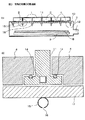
図1(a)は、本発明の実施の形態1のプラズマ処理装置の断面図、(b)は(a)のA部拡大図、(c)は(a)の上面図である。
1は導波管、例えば断面方形状の矩形導波管、2は導波管アンテナを構成する複数のスロット、3は電磁波源であり、例えば2.45GHzのマイクロ波を出力するマイクロ波源、4は電磁波を透過する材料例えば石英、ガラス、セラミック等の誘電体からなる長方形状電磁波放射窓(電磁波導入窓)、5は真空容器(プラズマ発生室)、6はプラズマ処理するための処理ガスのガス導入口、7はガス排気口、8はプラズマ処理される被処理基板、9は基板支持台(ステ−ジ)、10は真空容器5の天板、11は上記の各長方形状電磁波放射窓4を気密に支持するために設けられた梁体、17はマイクロ波源3から複数の矩形導波管1に電磁波を分配する電磁波分配用導波管部である。
上記電磁波放射窓(電磁波導入窓)4は、比較的薄くして耐圧を持たせるために複数に分割している。この実施の形態1では、複数のスロット2と対向するように各電磁波放射窓4は、長方形状に構成され、複数枚の電磁波放射窓4により、真空容器5の天板10を構成している。
梁体11には、プラズマ反応熱により電磁波放射窓4が加熱され、変形して気密性が劣化するのを保護するために熱良導体例えばアルミニウムで構成し、温調するための機構例えば冷媒の流路を内蔵して設けることができる。冷媒としては、流水が望ましく、水路を梁体11内に形成し、梁体11を所定の温度に温調することができる。換言すれば、一枚の電磁波放射窓4の大きさは、所望する厚さと、温調可能な大きさに設計される。
隣り合うスロット2間の距離は、真空容器5内に均一なプラズマが発生するように、または電磁波が真空容器5内に均一に放射されるように設けられる。スロット2は、プラズマ処理する全面積にわたりほぼ均一に分布して設けられる。隣り合う導波管1の対向する管壁の内面間の距離は、真空容器5内に均一に電磁波が放射されるように、一つの導波管1の対向する内面間の幅以内に設けられる。真空容器5内に均一に電磁波を放射することは、真空容器5内に形成されるプラズマ密度を均一にする。各導波管1と電磁波放射窓4の長軸方向がほぼ一致し、上記長軸方向の長さもほぼ一致し、長軸の周期もほぼ一致して構成されている、電磁波放射窓4の長軸方向の長さが、導波管1の長軸方向の長さより短く構成されている。
Hereinafter, embodiments of the present invention will be described in detail with reference to the drawings. In the drawings described below, those having the same functions are denoted by the same reference numerals, and repeated description thereof will be omitted.
1A is a cross-sectional view of the plasma processing apparatus according to the first embodiment of the present invention, FIG. 1B is an enlarged view of a portion A of FIG. 1A, and FIG. 1C is a top view of FIG.
1 is a waveguide, for example, a rectangular waveguide having a rectangular cross section, 2 is a plurality of slots constituting a waveguide antenna, 3 is an electromagnetic wave source, for example, a microwave source for outputting a microwave of 2.45 GHz, 4 Is a rectangular electromagnetic wave radiation window (electromagnetic wave introduction window) made of a dielectric material such as quartz, glass, ceramic or the like that transmits electromagnetic waves, 5 is a vacuum vessel (plasma generation chamber), and 6 is a processing gas for plasma processing. An
The electromagnetic wave radiation window (electromagnetic wave introduction window) 4 is divided into a plurality of parts in order to make it relatively thin and have a withstand voltage. In the first embodiment, each electromagnetic
The
The distance between the
プラズマが生成される真空容器5には、原料ガスを導入するためのガス導入口6と、導入されたガスを排気するためのガス排気口7が接続されている。
真空容器5は、上壁面として電磁波放射窓4により気密容器が構成されている。
マイクロ波源3の発振器にて発振されたマイクロ波は、直線状の電磁波分配用導波管部17により複数の導波管1に分配、伝送され、導波管アンテナを構成するスロット2から電磁波放射窓4を介して真空容器5内に放射される。多数の導波管1は、電磁波分配用導波管部17からほぼ直角に分岐している。この電磁波分配用導波管部17からこの多数の導波管1が分岐している面は、電界面(E面)18、すなわち、磁界面(H面)19に垂直な面、あるいは電磁波分配用導波管部17が本実施の形態1のように矩形導波管の場合は、幅が短い方の導波管面とも言える。このため、電磁波の伝播方向は、電磁波分配用導波管部17部分でほぼ直角に曲げられる。これにより、電磁波の伝播方向がほぼ直角に曲がらない前記第4の従来装置および第5の従来装置に比較して、多数の導波管1に分岐させることができ、大面積の基板に対応しやすく、また分岐部分のフットプリントが小さい特長がある。
また、電磁波分配用導波管部17と多数の導波管1とは、ほぼ同一平面上にある。この方式は、電磁波分配用導波管部17と多数の導波管1が重なって配置される多層型に対し、1層型と呼ばれる。多層型に比較し1層型は、装置の高さを低くすることができ、装置をコンパクトにすることができる。また、後述のように、1つの金属ブロックから電磁波分配用導波管部17および多数の導波管1を削り出して作製することにより安価に作製できる特長がある。
A
The airtight container is constituted by the electromagnetic
The microwave oscillated by the oscillator of the
Further, the electromagnetic wave
例えば、電磁波放射窓4の幅w4は10cm、スロット2の幅w2はそれより数mm小さい。電磁波放射窓4を複数設けて幅w4を狭くすることは、下記のように、電磁波放射窓4の厚さを薄くすることができ、電磁波の損失を小さくすることができると共に、大型基板に対応する大型プラズマ処理装置を提供することが可能となる。
真空容器5内を低圧力にすると、電磁波放射窓4には、ほぼ大気圧と、ほぼ真空に近い圧力とのガス圧力差、つまり、約9.80665×10⁴Pa(1kg/cm2)の力がかかる。このため、電磁波放射窓4の厚さを、この力に耐え得るような厚さにする必要がある。
下記表1に示すように、電磁波放射窓4を例えば直径300mmの円形状あるいは250mm角の矩形状の合成石英板で形成すると、該電磁波放射窓4の厚さは約30mm必要になる。電磁波放射窓4の厚さが厚くなると、電磁波の損失が大きくなる。ましてや、1m角程度の大型基板に対応するプラズマ処理装置の場合では、電磁波放射窓4の厚さが厚くなり過ぎ、実現不可能である。このため、本実施の形態1では、8cm×55cmの電磁波放射窓4を6個設け、これら6個の電磁波放射窓4と真空容器5との間で真空が保持されているようになっている。このため、電磁波放射窓4の厚さは、30mmとすることが可能となった。
For example, the width w 4 of the electromagnetic
When the inside of the
As shown in Table 1 below, when the electromagnetic

本実施の形態1にあっては、矩形導波管1の複数のスロット2に対応して電磁波放射窓4を複数設けたので、外気と真空容器5内との圧力差は、電磁波放射窓4の寸法により耐えられればよいので、電磁波放射窓4の厚さを薄くすることができる。したがって、大型のプラズマ処理装置を実現でき、大面積の基板を均一なプラズマ密度で処理することができる。また、矩形導波管1どうしを接して配置しているため、スロット2をプラズマ処理する全面積に渡り均一に分布させることが容易にできる。したがって、大面積の基板を均一なプラズマ密度で処理することができる。また、スロット2をプラズマ処理する全面積に渡り均一に分布させるというのは、例えばスロット2どうしの縦方向のピッチ、および横方向のピッチを同一にすることである。また、1台の電磁波源(ここでは、マイクロ波源3)から、電磁波分配用導波管部17を通じて複数の矩形導波管1へ電磁波を供給しているため、すべての矩形導波管1において周波数を同一とすることができ、均一なエネルギー密度を放射するようなアンテナを設計しやすい。周波数が異なると、電磁波の干渉を考慮して設計する必要がある。
さらに、複数のスロット2に共通する電磁波放射窓4を複数設けることにより、真空容器5の天板の加工費を低減でき、装置価格を低減することができる。
図1(d)は、矩形導波管1の別の構成例を示す断面図である。図1(a)に示すように、別部材で形成した複数の矩形導波管1を接して配置してもよいし、複数の矩形導波管1を接して配置した図1(d)に示すような1個の部材を用いてもよい。なお、本発明において、複数の矩形導波管1どうしを接して配置するという技術思想には、矩形導波管1どうしを数cm離す程度のことは当然含まれる。また、導波管1と電磁波分配用導波管部17とを1個の部材を用いて作製してもよい。
In the first embodiment, since a plurality of electromagnetic
Further, by providing a plurality of
FIG. 1D is a cross-sectional view illustrating another configuration example of the
本実施の形態1の考え方の基本は、マイクロ波を、電磁波分配用導波管部17により、これらとほぼ直角に分岐している複数の矩形導波管1を用いて、角型大面積の領域に分配し、スロット2から電磁波放射窓4を通して、角型大面積に均一なエネルギー密度でマイクロ波を放射し、均一なプラズマ密度のプラズマを発生させることにある。
上述の第3の従来装置では、その明細書に記載されているように(段落0028)、結合孔から等しいマイクロ波電力が放射され、プラズマが形成される。しかし、導波管が所定間隔を設けて配置されており、プラズマは拡散により拡がるため、プラズマ密度はガウス分布を持つ。このガウス分布を重ね合わせて、均一化を図っている。
つまり、本実施の形態1では、接した複数の矩形導波管1により、角型大面積の領域に均一なプラズマ密度のプラズマを発生させる。これに対して、上記第3の従来装置では、導波管をある間隔をあけ、ガウス分布の重なりでプラズマの均一化を図るものである。
この相違点を導波管の製作方法の違いで説明する。
本実施の形態1において、例えば有効処理面積70cm×60cmの場合を例にして説明する。このため、例えば矩形導波管1の具体的な製作方法として、70cm×60cm×4cmのアルミニウムブロックから、矩形導波管1内の幅が9cm、高さが3cmになるように、6本の矩形導波管1を削り出して作製した。つまり、この場合は、隣り合う矩形導波管1の壁は一体のものである(図1(d)参照)。
また、矩形導波管1を複数本作製し、これらが接するように組み立てる方法においても、本実施の形態1による導波管平面アンテナを作製することが可能である。
さらに、前述のように、これらの矩形導波管1を少しあけて作製しても、本実施の形態1による効果を得ることは可能である。
また、矩形導波管1の1本毎に対応して、図1(c)に示すように、矩形導波管1の幅とほぼ同等の幅(ここでは、矩形導波管1の幅より狭い幅)を有する電磁波放射窓4を配置し、矩形導波管1と電磁波放射窓4の長軸方向がほぼ一致し、矩形導波管1と電磁波放射窓4の長軸方向の長さがほぼ一致し、矩形導波管1と電磁波放射窓4の長軸の周期がほぼ一致している。このように電磁波放射窓4を矩形導波管1の1本毎に形成し、電磁波放射窓4を矩形導波管1との長軸方向と長さおよび周期を対応させることにより、電磁波放射窓4を複数に分割しながら、梁体11で電磁波が遮られることなく、電磁波を有効に真空容器5内へ導入できる。
また、電磁波放射窓4の長軸方向の長さを、矩形導波管1の長軸方向の長さより短くすることもできる。この場合、電磁波放射窓4を支持する真空容器5の天板10の梁体11を縦横方向に交差して形成でき、矩形導波管1よりも長さが短い小さな電磁波放射窓4を形成できるので、電磁波放射窓4の厚さをより薄くできる。
The basic idea of the first embodiment is that the microwave is distributed by the electromagnetic wave
In the third conventional device described above, as described in the specification (paragraph 0028), equal microwave power is emitted from the coupling hole, and a plasma is formed. However, since the waveguides are arranged at predetermined intervals and the plasma spreads by diffusion, the plasma density has a Gaussian distribution. This Gaussian distribution is superimposed to achieve uniformity.
That is, in the first embodiment, the plasma having a uniform plasma density is generated in a rectangular area having a large area by the plurality of
This difference will be described with reference to a difference in a method of manufacturing a waveguide.
In the first embodiment, an example in which the effective processing area is 70 cm × 60 cm will be described as an example. For this reason, for example, as a specific method for manufacturing the
Also, in a method of manufacturing a plurality of
Further, as described above, even if these
Further, as shown in FIG. 1C, the width of the
Further, the length of the electromagnetic
また、矩形導波管1に電磁波を供給するマイクロ波源3が1台であり、マイクロ波源3の周波数は2.45GHzである。マイクロ波源3の周波数としては、2.45GHzのものが量産され、現在、標準となっており、安価であり、種類も豊富である。
なお、本実施の形態1のプラズマ処理装置では、プラズマ処理として、プラズマ酸化、プラズマ成膜、プラズマエッチング、あるいはプラズマアッシングを行うことが可能である。
また、本装置を用いることにより、角型大面積の基板のプラズマ処理ができる。また、本プラズマは、高電子密度で電子温度が低くかつ均一性が良いため、非常に良好なプラズマ酸化、プラズマエッチング、プラズマ成膜のプラズマ処理方法を提供できる。
Further, there is one
In the plasma processing apparatus according to the first embodiment, as the plasma processing, plasma oxidation, plasma film formation, plasma etching, or plasma ashing can be performed.
In addition, by using the present apparatus, plasma processing of a substrate having a large square area can be performed. In addition, since the present plasma has a high electron density, a low electron temperature, and good uniformity, it is possible to provide a plasma treatment method of plasma oxidation, plasma etching, and plasma film formation that is very good.
実施の形態2
図2(a)は、本発明の実施の形態2のプラズマ処理装置の断面図、(b)は(a)の上面図である。
本実施の形態2は、誘電体からなる複数の電磁波放射窓4を支える梁体11(通常は金属からなる)を誘電体、例えば誘電体部材12で被うことにより、プラズマを梁体11部分にも拡がりやすくするためのものである。梁体11部分にプラズマを拡がりやすくするには、金属からなる梁体11でプラズマ中の電子等が消滅しないように、少なくとも梁体11の真空容器5の内面(内壁面)側を誘電体部材12で被うことにより達せられる。
本実施の形態2では、1個以上、ここでは1列9個×6列=54個の電磁波放射窓4に共通して接する、ここでは1枚の矩形板状の誘電体部材12が、真空容器5内に設けてある。
本実施の形態2にあっては、複数の電磁波放射窓4を支える金属製の梁体11が存在しても、複数のスロット2の全体で構成される導波管アンテナ全体の下部に設けた誘電体部材12中で電磁波が拡がりやすく、また、プラズマが金属の梁体11にさらされないため、誘電体部材12がない場合に比べてより均一性の良いプラズマを形成することができる。また、本実施の形態2では、誘電体部材12が1枚の場合を示したが、該誘電体部材12を複数枚に分割することも可能である。また、先にも述べたように、少なくとも梁体11の真空容器5の内面側を誘電体部材で被うことにより達せられる。また、電磁波放射窓4を構成する誘電体部材と、梁体11の内面側を被う誘電体部材とを一体に形成することも可能である。
FIG. 2A is a cross-sectional view of a plasma processing apparatus according to
In the second embodiment, the beam 11 (usually made of metal) that supports the plurality of electromagnetic
In the second embodiment, one or more rectangular plate-shaped
In the second embodiment, even if there is a
実施の形態3
図3(a)は、本発明の実施の形態3のプラズマ処理装置の断面図、(b)は(a)のB部の拡大図である。また、図4は、本プラズマ処理装置の水冷管の配置を示すための上面図である。さらに、図5は、本プラズマ処理装置の複数のガス導入口を有するガス導入管の配置を示すための上面図である。
13は電磁波放射窓4と真空容器5の梁体11との気密を封止するためのOリング、14は梁体11内に設けられ、温調用冷却水を流すための角筒状水冷管、15は真空容器5内にガスを流すためのガス導入管、16はガス導入管15の複数箇所(図5においてガス導入管15の設置箇所は図示省略)に設けられたガス導入口である。
本実施の形態3では、複数個の電磁波放射窓4どうしの間の、電磁波放射窓4を保持する梁体11内に水冷管14を設けている。プラズマにより真空容器5の梁体11や、電磁波放射窓4の気密を封止するOリング13が加熱され、変形したり損傷したりするため、冷却する必要がある。本実施の形態3では、梁体11に水冷管14を設けることにより、プラズマの発生を妨げることなく、効率良く冷却することができる。
FIG. 3A is a cross-sectional view of a plasma processing apparatus according to
13 is an O-ring for sealing airtightness between the electromagnetic
In the third embodiment, a
また、複数個の電磁波放射窓4どうしの間の、電磁波放射窓4を保持する梁体11下の真空容器5内に、複数のガス導入口16を設けている。これらのガス導入口16により、プラズマの発生を妨げることなく、ガスを大面積の基板8に均一に供給できるため、均一性の良いプラズマ処理を行うことができる。なお、このような構成の水冷管14、ガス導入管15およびガス導入口16は、いずれか一方を設けてもよいことはもちろんである。
Further, a plurality of
実施の形態4
図6(a)は、本発明の実施の形態4のプラズマ処理装置の断面図、(b)は(a)の上面図である。
マイクロ波源3の最大出力が十分な場合は、実施の形態1のようにマイクロ波源3は1台でマイクロ波を供給することが可能である。しかし、マイクロ波源3の出力により、処理面積が制限される。マイクロ波源3の最大出力には限界があるため、本実施の形態4のように、複数台(ここでは2台)のマイクロ波源3を設け、複数台のマイクロ波源3からマイクロ波を供給することにより、大電力化が可能となり、大面積を処理できるプラズマ処理装置が実現可能となる。
本実施の形態4のように、マイクロ波源3を2台設けることにより2倍の面積に対応できる。例えば、10kWの電磁波源を1台用いる場合、100cm×120cmの基板サイズまで可能であるが、10kWの電磁波源を2台用いると、140cm×170cmの基板サイズまで対応可能となる。また、プラズマ密度を高くすることができ、プラズマ処理時間を短縮できる。
FIG. 6A is a cross-sectional view of a plasma processing apparatus according to
When the maximum output of the
By providing two
しかし、複数台のマイクロ波源3を使用する場合、複数台のマイクロ波源3からのマイクロ波が影響を及ぼし、プラズマ特性が変化し、安定性が低下する。このため、複数台のマイクロ波源3の、隣接するマイクロ波源3の周波数が異なるように設定することにより、マイクロ波源3の影響を軽減し、干渉を防ぎ、安定性を増すことができる。
さらに、上述のように、マイクロ波源3としては、周波数が2.45GHzのものが量産されており、これを用いることにより、装置を安価に製造できる。2.45GHzのマイクロ波源3においても、わずかには周波数を変更することが可能であり、隣接するマイクロ波源3の周波数が異なるように設定することが可能である。
However, when a plurality of
Further, as described above, the
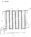
実施の形態5
図7は、本発明の実施の形態5のプラズマ処理装置の上面図である。
本実施の形態5では、電磁波源、例えばマイクロ波源3を4台にすることにより、マイクロ波源3が1台の場合に比較し、4倍の面積に対応できる。例えば、10kWの電磁波源を4台用いる場合、200cm×240cmの基板サイズまで対応可能となる。
FIG. 7 is a top view of the plasma processing apparatus according to the fifth embodiment of the present invention.
In the fifth embodiment, by using four electromagnetic wave sources, for example, four
実施の形態6
図8(a)は、本発明の実施の形態6のプラズマ処理装置の断面図、(b)は(a)の上面図である。
先にも述べたように、本発明において、複数の矩形導波管1どうしを接して配置するという技術思想には、矩形導波管1どうしを数cm離す程度のことは当然含まれる。本実施の形態6では、矩形導波管1の内面間の幅w1が9cmあるのに対し、隣り合う矩形導波管1の内面間の距離dを3cmとしたものである。この矩形導波管1の間隔は、電磁波をスロット2から電磁波放射窓4を通して真空容器5内に均一に放射するように配置されたものである。
矩形導波管1の間隔を変化させて発生させたプラズマ特性の発光状態を、真空容器5の下面に設置したCCDカメラで観察した。この実験によると、隣り合う矩形導波管1の内面間の距離dが、矩形導波管1の内面間の幅w1以内で近接して配置された場合、真空容器5内に均一にプラズマが発生した。この結果から、導波管の内面間の距離dが導波管の内面間の幅w1以内で近接して配置するのが良い。
FIG. 8A is a cross-sectional view of a plasma processing apparatus according to
As described above, in the present invention, the technical idea of arranging a plurality of
The light emission state of the plasma characteristics generated by changing the distance between the
実施の形態7
図9は、本発明の実施の形態7のプラズマ処理装置の上面図である。
本実施の形態7では、実施の形態6における電磁波源、例えばマイクロ波源3を4台にすることにより、マイクロ波源3が1台の場合に比較し、4倍の面積に対応させたものである。例えば、10kWの電磁波源を4台用いる場合、200cm×240cmの基板サイズまで対応可能となる。
FIG. 9 is a top view of the plasma processing apparatus according to the seventh embodiment of the present invention.
In the present seventh embodiment, the number of the electromagnetic wave sources, for example, the four
実施の形態8
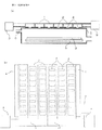
図10(a)は、本発明の実施の形態8のプラズマ処理装置の断面図、(b)は(a)の上面図である。
本実施の形態8では、マイクロ波源3の発振器にて発振されたマイクロ波は、直線状の矩形状の電磁波分配用導波管部17の対向する各壁面に分岐して左右の2方向の導波管1に分配、伝送され、導波管アンテナを構成するスロット2から電磁波放射窓4を介して真空容器5内に放射される。この実施の形態8においても、導波管1と電磁波分配用導波管部17とは、同一平面上に構成される。多数の導波管1は、電磁波分配用導波管部17から左右にほぼ直角に分岐している。図10(b)に示すように、この電磁波分配用導波管部17部分に、スロット2を設けてもよいし、設けた方がプラズマが均一に発生する。
本実施の形態8は、実施の形態1、2等と比較し、電磁波を左右に分配する電磁波分配用導波管部17の設計が難しいが、電磁波分配用導波管部17部が別に要らず、装置をコンパクトにすることができ、また、導波管全体の長さが短くて導波管の長さ方向のプラズマの均一性を取るのが容易な特長がある。
FIG. 10A is a cross-sectional view of the plasma processing apparatus according to the eighth embodiment of the present invention, and FIG. 10B is a top view of FIG.
In the eighth embodiment, the microwave oscillated by the oscillator of the
In the eighth embodiment, it is difficult to design the electromagnetic wave
実施の形態9
図11は、本発明の実施の形態9のプラズマ処理装置の上面図である。
本実施の形態9では、実施の形態8の電磁波源であるマイクロ波源3を4台にすることにより、マイクロ波源3が1台の場合に比較し、4倍の面積に対応させたものである。例えば、10kWの電磁波源を4台用いる場合、200cm×240cmの基板サイズまで対応可能となる。
FIG. 11 is a top view of the plasma processing apparatus according to the ninth embodiment of the present invention.
In the ninth embodiment, the number of the
実施の形態10
図12(a)は、本発明の実施の形態10のプラズマ処理装置の断面図、(b)は(a)の上面図である。なお、図12(a)は、図1(a)の断面図とは異なり、図10(b)の矢印C方向から見た断面図である。図12(a)と(b)は、ガス導入口6とガス排気口7の設置場所が対応していない。
前述のように、真空容器5内を低圧力にすると、電磁波放射窓4には、ほぼ大気圧と、ほぼ真空に近い圧力とのガス圧力差、つまり、約9.80665×10⁴Pa(1kg/cm2)の力がかかる。このため、電磁波放射窓4の厚さを、この力に耐え得るような厚さにする必要がある。例えば、70cm×60cmの電磁波放射窓4の場合には、石英ガラスを用いると、70mmの厚さにすれば、1枚の電磁波放射窓4で対応可能である。本実施の形態10は、この電磁波放射窓4が1枚の場合を示す。この場合、梁体11による電磁波の影響がない長所がある。ただし、電磁波放射窓4が1枚の場合、100cm角以上の基板サイズには、電磁波放射窓4の厚さが厚くなりすぎ、対応が困難である。
以上説明した実施の形態1〜10では、電磁波源は主にマイクロ波源を用いて説明したが、マイクロ波源に限定されるものではない。また、電磁波分配用導波管部を直線状のものを用いて説明したが、直線状に限定されるものではない。また、導波管も矩形に限定されない。
FIG. 12A is a cross-sectional view of a plasma processing apparatus according to
As described above, when the inside of the
In the first to tenth embodiments described above, the electromagnetic wave source is mainly described using a microwave source, but is not limited to a microwave source. Further, the description has been made using the linear waveguide portion for electromagnetic wave distribution, but the present invention is not limited to the linear waveguide portion. Further, the waveguide is not limited to a rectangular shape.
実施の形態11
次に、上記実施の形態のプラズマ処理装置を使用して、ガラス基板上に形成する液晶表示装置用の多結晶シリコン薄膜トランジスタ(Poly-Si TFT)の製作工程を説明する。
Next, a process of manufacturing a polycrystalline silicon thin film transistor (Poly-Si TFT) for a liquid crystal display device formed on a glass substrate using the plasma processing apparatus of the above embodiment will be described.
まず、多結晶シリコン薄膜トランジスタの位置付け、およびゲート絶縁膜の要求仕様について述べる。
低温ポリSi(多結晶シリコン)薄膜トランジスタ(Poly-Si TFT)は、従来のアモルファス薄膜トランジスタ(a-Si TFT)より電気的特性が高く、液晶表示装置用ガラス基板上に種々の電子回路を形成できるため、非常に期待されている。この低温ポリSiTFTの鍵となる技術の1つがゲート絶縁膜の形成である。
低温ポリSiTFT用と集積回路用のゲート絶縁膜は同様の用途に用いられているが、要求仕様はまったく異なる。まず、プロセス温度は集積回路用950℃以上に対し、TFTはガラスを用いた場合、600℃以下、プラスチックを用いた場合、200℃以下にする必要がある。また、基板面積は、直径30cmの集積回路用単結晶Siウエハに対し、TFTではガラス基板約70cm×90cmの場合、約9倍の面積であり、将来さらに大きな面積をカバーする必要がある。
一方、表面凹凸については、集積回路用単結晶Siウエハでは原子的に平坦にすることが可能であり、将来の目標は0.1nmとなっている。これに対し、低温ポリSiの表面凹凸は、溶けたSiが液相から核を始点として固体に変わって結晶成長するときに体積が膨張し、最後に結晶粒がぶつかった粒界で盛り上がり約50nmの突起が形成される。また、チャネル部の島状のポリSiの段差は50nm〜200nmである。このため、低温ポリSiTFT用として、この突起および段差を十分カバーできるゲート絶縁膜の開発が必要である。
次に、ゲート絶縁膜の電気的欠陥密度の要求仕様の差異について述べると、単一素子の面積は、集積回路のうちPCプロセッサの1.5cm2に対し、15インチ液晶ディスプレイは900cm2と600倍である。トランジスタの中心部であるチャネル面積は、集積回路用で0.14μm×0.14μmに対し、最小TFT1.0μm×1.0μmで、周辺回路ではさらに大きなものがあり、約100倍程度である。液晶画面内のTFTの数は、UXGAで1600×1200×3=576万個ある。取り込む回路により異なるが、TFT基板に取り込む周辺集積回路に含まれるトタンジスタの数は、数百万個のオーダーと思われる。このため、周辺回路を含んだシステムパネルに含まれるトランジスタの合計数は、周辺集積回路に比較して数倍である。これらのことより、単一素子内のチャネル面積の合計は、低温ポリSiTFTの場合、集積回路と比較しておよそ数百倍と予測される。つまり、TFT単一パネルの良品率を集積回路単一チツプと同等にするには、ゲート絶縁膜の電気的欠陥密度を数百分の1にする必要がある。
以上説明したように、低温ポリSiTFTの場合は集積回路の場合と異なり、下記の要求仕様を満たす低温ポリSiTFTに適した絶縁膜形成技術の開発が不可欠である。
(1)600℃以下の低温で形成する。
(2)大面積、かつ大きな凹凸を均一性よくカバーする。
(3)電気的欠陥密度を大幅に改善する。
(4)良好なSi/SiO2界面を形成する。
このため、角型大面積基板に、高密度・低損傷なプラズマを用いて、酸化、成膜およびエッチングを行うことができるプラズマ処理装置が望まれている。
First, the positioning of the polycrystalline silicon thin film transistor and the required specifications of the gate insulating film will be described.
Low-temperature poly-Si (polycrystalline silicon) thin-film transistors (Poly-Si TFTs) have higher electrical characteristics than conventional amorphous thin-film transistors (a-Si TFTs) and can form various electronic circuits on glass substrates for liquid crystal displays. , Very expected. One of the key technologies of the low-temperature poly-Si TFT is formation of a gate insulating film.
Gate insulating films for low-temperature poly-Si TFTs and integrated circuits are used for similar applications, but the required specifications are completely different. First, the process temperature must be 950 ° C. or higher for integrated circuits, 600 ° C. or lower when glass is used for TFT, and 200 ° C. or lower when plastic is used. The substrate area is about 9 times as large as that of a glass substrate of about 70 cm × 90 cm with respect to a single crystal Si wafer for an integrated circuit having a diameter of 30 cm, and it is necessary to cover a larger area in the future.
On the other hand, surface irregularities can be made atomically flat in a single crystal Si wafer for integrated circuits, and the future target is 0.1 nm. On the other hand, the surface unevenness of the low-temperature poly-Si is such that when the melted Si changes from a liquid phase to a solid starting from the nucleus and grows as a crystal, the volume expands, and finally the crystal grain swells at a grain boundary where the crystal grains collide with about 50 nm. Projections are formed. The step of the island-shaped poly-Si in the channel portion is 50 nm to 200 nm. For this reason, it is necessary to develop a gate insulating film for low-temperature poly-Si TFTs that can sufficiently cover the protrusions and steps.
Next, we describe differences required specifications of the electrical defect density of the gate insulating film, the area of a single element, with respect to 1.5 cm 2 of the PC processor of the integrated circuit 15-inch LCD display 900 cm 2 and 600 It is twice. The channel area, which is the central part of the transistor, is 0.14 μm × 0.14 μm for integrated circuits, and the minimum TFT is 1.0 μm × 1.0 μm, and some peripheral circuits are even larger, about 100 times. The number of TFTs in the liquid crystal screen is 1600 × 1200 × 3 = 5.76 million in UXGA. The number of transistors included in the peripheral integrated circuit to be taken into the TFT substrate is considered to be on the order of several million, although it depends on the circuit to be taken in. Therefore, the total number of transistors included in the system panel including the peripheral circuit is several times that of the peripheral integrated circuit. From these facts, the total channel area in a single device is estimated to be several hundred times larger in the case of a low-temperature poly-Si TFT than in an integrated circuit. That is, in order to make the yield rate of the TFT single panel equal to that of the integrated circuit single chip, it is necessary to reduce the electrical defect density of the gate insulating film to several hundredths.
As described above, in the case of the low-temperature poly-Si TFT, unlike the case of the integrated circuit, it is essential to develop an insulating film forming technique suitable for the low-temperature poly-Si TFT satisfying the following required specifications.
(1) It is formed at a low temperature of 600 ° C. or less.
(2) Cover large areas and large irregularities with good uniformity.
(3) Significantly improve electrical defect density.
(4) Form a good Si / SiO 2 interface.
Therefore, a plasma processing apparatus capable of performing oxidation, film formation, and etching on a rectangular large-area substrate using high-density and low-damage plasma is desired.
次に、上記実施の形態のプラズマ処理装置を用いて、ガラス基板上に形成する液晶表示用の多結晶シリコン薄膜トランジスタ(Poly-Si TFT)の製作工程を説明する。
図13は、本発明を液晶表示装置用のnチャンネル型、pチャンネル型の多結晶シリコン薄膜トランジスタに適用した場合のプロセスフロー図、図14(a)〜(e)は、それぞれ各プロセスにおける素子断面図である。
ガラス基板200(図14)は、大きさ700mm×600mm×1.1mmのガラス板を用いた。
図14(a)に示すように、洗浄したガラス基板200上に、TEOSガスを用い、PE−CVD法(プラズマCVD法)により厚さ200nmの酸化シリコン膜(SiO2膜)をベースコート膜201として形成した(図13のS1)。
その後、SiH4およびH2ガスを用い、PE−CVD法によりアモルファスシリコン膜を厚さ50nm成膜した(S2)。
このアモルファスシリコン膜は、5〜15原子%の水素を含むため、そのままレーザーを照射すると、水素が気体となり、急激に体積膨張して、膜が吹き飛ぶ。このため、アモルファスシリコン膜を形成したガラス基板200を、水素の結合が切れる350℃以上で、約1時間保って水素を逃がした(S3)。
その後、キセノンクロライド(XeCl)エキシマレーザー光源から波長308nmのパルス光(670mJ/パルス)を、光学系により0.8mm×130mmに成形して360mJ/cm2の強度で、前記ガラス基板200上のアモルファスシリコン膜に照射した。アモルファスシリコンは、レーザー光を吸収して溶融し、液相になった後、温度が下がり固化し、多結晶シリコンが得られた。レーザー光は200Hzのパルスであり、溶融と固化は1パルスの時間内で終わる。このため、レーザー照射により、1パルス毎に溶融+固化を繰り返すことになる。ガラス基板200を移動させながらレーザー照射することにより、大面積を結晶化できる。特性のバラツキを抑えるため、個々のレーザー光の照射領域を95〜97.5%重ね合わせて照射した(S4)。
この多結晶シリコン層を、フォトリソグラフィー工程(S5)、エッチング工程(S6)により、図14(a)に示すように、ソース、チャネル、ドレインに対応する島状多結晶シリコン層216にパターンニングし、nチャネルTFT領域202、pチャネルTFT領域203、画素部TFT領域204を形成した(ここまで、図14(a))。
Next, a process of manufacturing a polycrystalline silicon thin film transistor (Poly-Si TFT) for liquid crystal display formed on a glass substrate using the plasma processing apparatus of the above embodiment will be described.
FIG. 13 is a process flow diagram when the present invention is applied to an n-channel type and a p-channel type polycrystalline silicon thin film transistor for a liquid crystal display device, and FIGS. 14 (a) to 14 (e) are element cross sections in each process. FIG.
As the glass substrate 200 (FIG. 14), a glass plate having a size of 700 mm × 600 mm × 1.1 mm was used.
As shown in FIG. 14A, a 200-nm-thick silicon oxide film (SiO 2 film) is formed as a
Thereafter, an amorphous silicon film having a thickness of 50 nm was formed by a PE-CVD method using SiH 4 and H 2 gases (S2).
Since this amorphous silicon film contains 5 to 15 atomic% of hydrogen, if the laser is irradiated as it is, the hydrogen becomes a gas, the volume expands rapidly, and the film is blown off. For this reason, hydrogen was released from the
Thereafter, a pulse light (670 mJ / pulse) having a wavelength of 308 nm from a xenon chloride (XeCl) excimer laser light source is formed into 0.8 mm × 130 mm by an optical system and has an intensity of 360 mJ / cm 2 on the
This polycrystalline silicon layer is patterned into an island-shaped
この後、Poly-Si TFTの最も重要なチャネル領域上に形成される絶縁膜との界面および絶縁膜を形成する(S7)。
プラズマ処理装置としては、実施の形態1に示した図1の装置を用いた。
上記のベースコート膜201(図14(a))上に島状多結晶シリコン層216をもつガラス基板200を、温度を350℃にした支持台10にセットした。
その後、反応室にArガスと酸素ガスをAr/(Ar+O2)=95%の比率で混合したガスを導入し、80Paに保つ。その後、2.45GHzのマイクロ波電源から5kWの電力を投入し、酸素プラズマを立てて、プラズマ酸化を行う。
酸素プラズマでは、酸素ガスを反応性の高い酸素原子活性種に分解し、この酸素原子活性種により島状多結晶シリコン層216が酸化され、ゲート絶縁膜205(図14(b)。第1の絶縁膜)となるSiO2からなる光酸化膜が形成される。3分間で膜厚約3nmの第1ゲート絶縁膜205(第1の絶縁膜)が形成できた(S8)。
次に、プラズマ酸化用のガスを排気後、真空を破らずに連続してSiO2を成膜するため、基板温度350℃のまま、TEOSガス流量を30sccm、酸素ガス流量を7500sccm、成膜室25内の圧力を267Pa(2Torr)、マイクロ波電源電力を450Wとし、プラズマCVD法によりSiO2膜からなる第2ゲート絶縁膜206(第2の絶縁膜)を成膜した。2分間で膜厚30nmの第2ゲート絶縁膜206を成膜した(S9)。
プラズマ酸化工程(S8)および高密度・低損傷なプラズマCVD法による第1ゲート絶縁膜205の成膜工程(S9)を、連続して真空中で、しかも生産性を落とさずに行なうことができる。これにより、半導体(島状多結晶シリコン層216)と第1ゲート絶縁膜205との良好な界面を形成すると共に、厚くて実用に耐える絶縁膜を速く形成できた。プラズマ酸化とプラズマCVD法による成膜を別の反応室で行うことも可能である。
Thereafter, an interface with an insulating film formed on the most important channel region of the Poly-Si TFT and an insulating film are formed (S7).
As the plasma processing apparatus, the apparatus shown in FIG. 1 described in
The
Thereafter, a gas in which Ar gas and oxygen gas are mixed at a ratio of Ar / (Ar + O 2 ) = 95% is introduced into the reaction chamber, and the gas is maintained at 80 Pa. Thereafter, power of 5 kW is supplied from a microwave power supply of 2.45 GHz, oxygen plasma is generated, and plasma oxidation is performed.
In the oxygen plasma, the oxygen gas is decomposed into highly reactive oxygen atom active species, and the island-shaped
Next, in order to continuously form a SiO 2 film without breaking the vacuum after exhausting the gas for plasma oxidation, the TEOS gas flow rate is 30 sccm, the oxygen gas flow rate is 7500 sccm, and the film formation chamber is kept at the substrate temperature of 350 ° C. A second gate insulating film 206 (second insulating film) made of a SiO 2 film was formed by a plasma CVD method with the pressure in the
The plasma oxidation step (S8) and the step (S9) of forming the first
この後は、従来と同じ工程によりPoly-Si TFTを形成した。
まず、ガラス基板200を基板温度350℃で、2時間、窒素ガス中でのアニールにより、SiO2膜からなる第1ゲート絶縁膜205の高密度化を行なう(S10)。高密度化処理で、SiO2膜の密度が高くなり、リーク電流、耐圧が向上する。
その後、スパッタ法によりTiをバリア金属として100nm成膜した後、同様にスパッタ法によりAlを400nm成膜した(S11)。このAlからなる金属層を、フォトリソグラフィー法(S12)によりパターニングを行い(S13)、図14(c)に示すように、ゲート電極207を形成した。
その後、フォトリソグラフィー工程でpチャネルTFT250のみをフォトレジスト(図示せず)で覆った(S14)。次に、イオンドーピング法により、ゲート電極207をマスクとして、燐を80keVで6×10¹⁵/cm2をnチャネルTFT260のn+ソース・ドレインコンタクト部209にドープした(S15)。
その後、フォトリソグラフィー工程でnチャネルTFT領域202および画素部TFT領域204のnチャネルTFT260をフォトレジストで覆い(S18)、イオンドーピング法により、ゲート電極207をマスクとして、ボロンを60keV、1×10¹⁶/cm2でpチャネル領域203(図14(a))のpチャネルTFT250(図14(c))のP+ソース・ドレインコンタクト部210にドープした(S17)。
その後、ガラス基板200を基板温度350℃で2時間アニールし、イオンドープした燐とボロンを活性化した(S18)。そして、TEOSガスを用いたプラズマCVD法でSiO2からなる層間絶縁膜208を成膜した(S19)(図6(c))。
Thereafter, a Poly-Si TFT was formed by the same process as the conventional method.
First, the density of the first
Then, after forming a film with a thickness of 100 nm using Ti as a barrier metal by the sputtering method, a film of Al was formed in a thickness of 400 nm in the same manner by the sputtering method (S11). The metal layer made of Al was patterned by photolithography (S12) (S13), and a
Thereafter, only the p-
Thereafter, the n-
Thereafter, the
次に、第2ゲート絶縁膜206、層間絶縁膜208に、フォトリソグラフィー工程(S20)およびエッチング工程(S21)で、n+ソース・ドレインコンタクト部209およびP+ソース・ドレインコンタクト部210へのコンタクトホールを図14(d)に示すようにパターニングした。そして、Tiをバリア金属(図示せず)として膜厚100nmスパッタした後、Alを膜厚400nmスパッタし(S22)、フォトリソグラフィー法(S23)およびエッチング工程(S24)によりソース電極213、ドレイン電極212をパターニングした(図14(d))。
Next, the second
更に、図14(e)に示すように、プラズマCVD法でSiO2膜からなる保護膜211を膜厚300nm成膜し(S25)、画素部TFT204領域(図14(a))のnチャネルTFT260(図14(c))のドレイン部212にITOからなる画素電極214(後述する)との接続用のコンタクトホールを、フォトリソグラフィー工程(S26)およびエッチング工程(S27)で、パターニングした。
この後、枚様式マルチチャンバスパッタ装置内で、基板温度350℃、H2ガス流量を1000sccm、ガス圧を173Pa(1.3Torr)、RF電源電力を450Wで、3分間、水素プラズマ処理を行った(S28)。
その後、別の反応室に移動させ、ITOを150nm成膜した(S29)。ITOを画素電極214としてフォトリソグラフィー工程(S30)およびエッチング工程(S31)でパターニングすることにより、TFT基板215は完成し(図14(e))、基板検査を行なった(S32)。
Further, as shown in FIG. 14E, a
Thereafter, a hydrogen plasma treatment was performed for 3 minutes at a substrate temperature of 350 ° C., a H 2 gas flow rate of 1000 sccm, a gas pressure of 173 Pa (1.3 Torr), and an RF power supply of 450 W in a multi-chamber sputtering apparatus. (S28).
Thereafter, the substrate was moved to another reaction chamber, and a film of ITO was formed to a thickness of 150 nm (S29). By patterning the ITO as a
このTFT基板215およびカラーフィルタが形成されたガラス基板(図示せず)に対し、ポリイミドを塗布し、ラビングした後、これらの基板を貼り合わせた。その後、この貼り合わせた基板を、各パネルに分断した。
これらのパネルを真空槽に入れ、皿に入れた液晶の中にパネルの注入口を浸し、槽に空気を導入することにより、その圧力で液晶をパネルに注入した。その後、注入口を樹脂で封止することにより、液晶パネルは完成した(S33)。
その後、偏向板の貼り付け、周辺回路、バックライト、ベゼル等の取り付けにより、液晶モジュールが完成した(S35)。
この液晶モジュールは、パソコン、モニター、テレビ、携帯端末等に使用できる。
このとき、TFTの閾値電圧は、プラズマ酸化膜が無く、通常のプラズマCVD法によりSiO2を成膜した従来の場合は、1.9V±0.8Vであったが、本実施の形態11においては、多結晶シリコン膜中にシリコン酸化膜とシリコン膜の界面が形成されるため、シリコン酸化膜と多結晶シリコン(島状多結晶シリコン層216)の良好な界面特性が得られ、また絶縁膜バルク特性の改善により、閾値電圧は1.5V±0.6Vに改善された。閾値電圧のバラツキが減少したため、良品率が大きく向上した。また、プラズマ酸化膜と、高密度・低損傷なプラズマCVD膜との積層構造により、カバレッジが良く、かつプラズマCVD法による膜の特性がよいため、ゲート絶縁膜の膜厚を従来の80〜100nmから、30nmと約1/3に薄くでき、オン電流を約3倍に向上できた。
また、ガラス基板上にSi単結晶ウエハ(P型、8〜12Ω・cm、直径150mm、(100))を置き、実施の形態11と同じ方法でゲート絶縁膜を形成した。その後、アルミニウムを、直径1mmの穴を設けたマスクを介して、低抵抗加熱蒸着した。その後、96%の窒素ガスと4%の水素ガスの混合ガス中で、400℃、30分焼成した。このMOS構造素子を用いて、界面準位密度を測定したところ、3×1010cm−2eV−1と、熱酸化膜と同等の良好な界面特性が得られた。
Polyimide was applied to the
These panels were placed in a vacuum tank, the inlet of the panel was immersed in the liquid crystal in a dish, and air was introduced into the tank, whereby the liquid crystal was injected into the panel at that pressure. Thereafter, the liquid crystal panel was completed by sealing the injection port with resin (S33).
Thereafter, a liquid crystal module was completed by attaching a deflection plate and attaching peripheral circuits, a backlight, a bezel, and the like (S35).
This liquid crystal module can be used for personal computers, monitors, televisions, portable terminals, and the like.
At this time, the threshold voltage of the TFT was 1.9 V ± 0.8 V in the conventional case in which no plasma oxide film was formed and SiO 2 was formed by a normal plasma CVD method. Since the interface between the silicon oxide film and the silicon film is formed in the polycrystalline silicon film, good interface characteristics between the silicon oxide film and the polycrystalline silicon (the island-like polycrystalline silicon layer 216) can be obtained. The threshold voltage has been improved to 1.5V ± 0.6V due to the improvement of the bulk characteristics. Since the variation in the threshold voltage was reduced, the yield rate was significantly improved. In addition, a stacked structure of a plasma oxide film and a high-density and low-damage plasma CVD film provides good coverage and good characteristics of a film formed by a plasma CVD method. Therefore, the thickness can be reduced to about 1/3 of 30 nm, and the on-current can be improved about three times.
A single-crystal Si wafer (P type, 8 to 12 Ω · cm, diameter 150 mm, (100)) was placed on a glass substrate, and a gate insulating film was formed in the same manner as in
本発明による上記実施の形態1〜11によれば、上で説明したガラスを基板とする液晶ディスプレイパネルにおける低温ポリSiTFTのチャネル形成用単結晶Si層と良好な界面特性を有する薄いゲート絶縁膜を、プラズマ酸化により形成するのに非常に有効なプラズマ処理装置およびプラズマ処理方法を提供することができる。 According to the first to eleventh embodiments of the present invention, a thin gate insulating film having good interface characteristics with a single-crystal Si layer for forming a channel of a low-temperature poly-Si TFT in a glass-based liquid crystal display panel described above is provided. It is possible to provide a plasma processing apparatus and a plasma processing method which are very effective for forming by plasma oxidation.
また、以上説明した実施の形態1〜11は、本発明の理解を容易にするために記載されたものであって、本発明を限定するために記載されたものではない。例えば、電磁波源は、主にマイクロ波源を用いて説明したが、マイクロ波源に限定されるものではない。また、電磁波分配用導波管部を直線状のものを用いて説明したが、直線状に限定されるものではなく、曲線状や折れ曲がった形状等でもよい。また、導波管の形状も矩形に限定されない。したがって、上記実施の形態に開示された各要素は、本発明の技術的範囲に属する全ての設計変更や均等物をも含む趣旨である。 The first to eleventh embodiments described above are described for facilitating the understanding of the present invention, and are not described for limiting the present invention. For example, the electromagnetic wave source has been mainly described using a microwave source, but is not limited to a microwave source. In addition, the description has been made using the linear waveguide portion for electromagnetic wave distribution, but the present invention is not limited to the linear shape, and may be a curved shape or a bent shape. Further, the shape of the waveguide is not limited to a rectangle. Therefore, each element disclosed in the above embodiment is intended to include all design changes and equivalents belonging to the technical scope of the present invention.
大型の被処理基板に対して、膜堆積、表面改質、あるいはエッチング等のプラズマ処理を施すプラズマ密度が均一なプラズマ処理装置およびプラズマ処理方法を提供でき、特に液晶ディスプレイ、EL、プラズマディスプレイ等の各種ディスプレイの製造に利用して好適である。 It is possible to provide a plasma processing apparatus and a plasma processing method with a uniform plasma density for performing plasma processing such as film deposition, surface modification, or etching on a large substrate to be processed, and in particular, a liquid crystal display, an EL, a plasma display, etc. It is suitable for use in manufacturing various displays.
1…矩形導波管、2…スロット、3…マイクロ波源、4…電磁波放射窓、5…真空容器、6…ガス導入口、7…ガス排気口、8…被処理基板、9…基板支持台、10…天板、11…梁体、12…誘電体部材、13…Oリング、14…水冷管、15…ガス導入管、16…ガス導入口、17…電磁波分配用導波管部、18…電界面(E面)、19…磁界面(H面)、
71…同軸伝送路、72…スロット、73…円形マイクロ波放射板、74…電磁波放射窓、75…真空容器、76…ガス導入口、77…ガス排気口、78…基板、79…基板支持台、
81…矩形導波管、82…スロット、83…マイクロ波源、84…電磁波放射窓、85…真空容器、86…ガス導入口、87…ガス排気口、88…基板、89…基板支持台、110…矩形導波管の反射面、111…矩形導波管のH面、
101…矩形導波管、102…結合孔、104…電磁波放射窓、105…真空容器、
200…ガラス基板
201…ベースコート膜
202…nチャネルTFT領域
203…pチャネルTFT領域
204…画素部TFT領域
205…第1ゲート絶縁膜
206…第2ゲート絶縁膜
207…ゲート電極
208…層間絶縁膜
209…n+ソース・ドレインコンタクト部
210…P+ソース・ドレインコンタクト部
211…保護膜
214…画素電極
215…TFT基板
250…pチャネルTFT
260…nチャネルTFT
1003…マイクロ波導入口、1004…マイクロ波導入窓、1023…導波管、1026…マイクロ波電源、1031…誘電体電路、1311…導入部、1312…整合部、1313…矩形部、1314…仕切り板、
1002…は反応室、1126…マイクロ波電源、1027…マイクロ波分配器、1028…導波管。
DESCRIPTION OF
71: Coaxial transmission line, 72: Slot, 73: Circular microwave radiation plate, 74: Electromagnetic radiation window, 75: Vacuum container, 76: Gas inlet, 77: Gas outlet, 78: Substrate, 79: Substrate support ,
81: rectangular waveguide, 82: slot, 83: microwave source, 84: electromagnetic radiation window, 85: vacuum vessel, 86: gas inlet, 87: gas exhaust port, 88: substrate, 89: substrate support, 110 ... Reflection surface of rectangular waveguide, 111 ... H surface of rectangular waveguide,
101: rectangular waveguide, 102: coupling hole, 104: electromagnetic wave radiation window, 105: vacuum vessel,
200
260 ... n-channel TFT
1003: microwave introduction port, 1004: microwave introduction window, 1023 ... waveguide, 1026 ... microwave power supply, 1031 ... dielectric circuit, 1311 ... introduction part, 1312 ... matching part, 1313 ... rectangular part, 1314 ... partition plate ,
1002 is a reaction chamber, 1126 is a microwave power supply, 1027 is a microwave distributor, 1028 is a waveguide.
Claims (27)
前記導波管に設けられ、導波管アンテナを構成する複数のスロットと、
誘電体からなる電磁波放射窓と、
真空容器とを具備し、
前記スロットから前記電磁波放射窓を通して前記真空容器内に放射された電磁波によってプラズマを生成し、プラズマ処理を行うプラズマ処理装置であって、
前記導波管が複数あり、前記導波管どうしが接して配置され、
電磁波源から複数の前記導波管に電磁波を分配する電磁波分配用導波管部を有し、
複数の前記電磁波放射窓と前記真空容器との間で真空が保持されていることを特徴とするプラズマ処理装置。 A waveguide,
A plurality of slots provided in the waveguide and constituting a waveguide antenna;
An electromagnetic radiation window made of a dielectric;
And a vacuum container,
A plasma processing apparatus that generates plasma by electromagnetic waves radiated into the vacuum vessel through the electromagnetic wave radiation window from the slot and performs plasma processing,
There are a plurality of the waveguides, the waveguides are arranged in contact with each other,
An electromagnetic wave distribution waveguide section that distributes electromagnetic waves from an electromagnetic wave source to the plurality of waveguides,
A plasma processing apparatus, wherein a vacuum is maintained between a plurality of the electromagnetic wave radiation windows and the vacuum container.
前記導波管に設けられ、導波管アンテナを構成する複数のスロットと、
この複数のスロットに対向して設けられた誘電体からなる電磁波放射窓と、
この電磁波放射窓を前記電磁波の入射面として設けられた真空容器とを具備し、
前記スロットから前記電磁波放射窓を通して前記真空容器内に放射された前記電磁波によってプラズマを生成し、プラズマ処理を行うプラズマ処理装置であって、
前記導波管が複数あり、
前記電磁波源から前記各導波管に前記電磁波を分配するための電磁波分配用導波管部を有し、
複数の前記導波管は、前記電磁波分配用導波管部の電界面(E面)または磁界面(H面)に垂直な面から分岐して設けられていることを特徴とするプラズマ処理装置。 An electromagnetic wave source that outputs an electromagnetic wave, an electromagnetic wave distribution waveguide portion that propagates the electromagnetic wave from the electromagnetic wave source, and a waveguide connected to the electromagnetic wave distribution waveguide portion;
A plurality of slots provided in the waveguide and constituting a waveguide antenna;
An electromagnetic wave radiation window made of a dielectric material provided opposite to the plurality of slots,
A vacuum container provided with the electromagnetic wave radiation window as an incident surface of the electromagnetic wave,
A plasma processing apparatus that generates plasma by the electromagnetic wave radiated into the vacuum vessel through the electromagnetic wave radiation window from the slot and performs plasma processing,
There are a plurality of said waveguides,
An electromagnetic wave distribution waveguide section for distributing the electromagnetic wave from the electromagnetic wave source to each of the waveguides,
The plasma processing apparatus, wherein the plurality of waveguides are provided by branching from a plane perpendicular to an electric field plane (E plane) or a magnetic field plane (H plane) of the electromagnetic wave distribution waveguide unit. .
前記導波管に設けられ、導波管アンテナを構成する複数のスロットと、
この複数のスロットに対向して設けられた誘電体からなる電磁波放射窓と、
この電磁波放射窓を前記電磁波の入射面として設けられた真空容器とを具備し、
前記スロットから前記電磁波放射窓を通して前記真空容器内に放射された前記電磁波によってプラズマを生成し、プラズマ処理を行うプラズマ処理装置であって、
前記導波管が複数あり、
前記電磁波源から前記各導波管に前記電磁波を分配するための電磁波分配用導波管部を有し、
前記電磁波分配用導波管部において、電磁波の伝播方向がほぼ直角に曲げられて、複数の前記導波管に電磁波を分配するようになっていることを特徴とするプラズマ処理装置。 An electromagnetic wave source that outputs an electromagnetic wave, an electromagnetic wave distribution waveguide portion that propagates the electromagnetic wave from the electromagnetic wave source, and a waveguide connected to the electromagnetic wave distribution waveguide portion;
A plurality of slots provided in the waveguide and constituting a waveguide antenna;
An electromagnetic wave radiation window made of a dielectric material provided opposite to the plurality of slots,
A vacuum container provided with the electromagnetic wave radiation window as an incident surface of the electromagnetic wave,
A plasma processing apparatus that generates plasma by the electromagnetic wave radiated into the vacuum vessel through the electromagnetic wave radiation window from the slot and performs plasma processing,
There are a plurality of said waveguides,
An electromagnetic wave distribution waveguide section for distributing the electromagnetic wave from the electromagnetic wave source to each of the waveguides,
The plasma processing apparatus according to claim 1, wherein, in the electromagnetic wave distribution waveguide portion, a propagation direction of the electromagnetic wave is bent at substantially a right angle to distribute the electromagnetic wave to the plurality of waveguides.
前記導波管に設けられ、導波管アンテナを構成する複数のスロットと、
この複数のスロットに対向して設けられた誘電体からなる電磁波放射窓と、
この電磁波放射窓を前記電磁波の入射面として設けられた真空容器とを具備し、
前記スロットから前記電磁波放射窓を通して前記真空容器内に放射された前記電磁波によってプラズマを生成し、プラズマ処理を行うプラズマ処理装置であって、
前記導波管が複数あり、
前記電磁波源から前記各導波管に前記電磁波を分配するための電磁波分配用導波管部を有し、
複数の前記導波管は、前記電磁波分配用導波管部の電界面から分岐して設けられ、
前記電磁波分配用導波管部と複数の前記導波管とは、ほぼ同一平面上に配置されていることを特徴とするプラズマ処理装置。 An electromagnetic wave source that outputs an electromagnetic wave, an electromagnetic wave distribution waveguide portion that propagates the electromagnetic wave from the electromagnetic wave source, and a waveguide connected to the electromagnetic wave distribution waveguide portion;
A plurality of slots provided in the waveguide and constituting a waveguide antenna;
An electromagnetic wave radiation window made of a dielectric material provided opposite to the plurality of slots,
A vacuum container provided with the electromagnetic wave radiation window as an incident surface of the electromagnetic wave,
A plasma processing apparatus that generates plasma by the electromagnetic wave radiated into the vacuum vessel through the electromagnetic wave radiation window from the slot and performs plasma processing,
There are a plurality of said waveguides,
An electromagnetic wave distribution waveguide section for distributing the electromagnetic wave from the electromagnetic wave source to each of the waveguides,
The plurality of waveguides are provided by branching from the electric field surface of the electromagnetic wave distribution waveguide portion,
The plasma processing apparatus according to claim 1, wherein the electromagnetic wave distribution waveguide section and the plurality of waveguides are arranged on substantially the same plane.
前記導波管に設けられ、導波管アンテナを構成する複数のスロットと、
この複数のスロットに対向して設けられた誘電体からなる電磁波放射窓と、
この電磁波放射窓を前記電磁波の入射面として設けられた真空容器とを具備し、
前記スロットから前記電磁波放射窓を通して前記真空容器内に放射された前記電磁波によってプラズマを生成し、プラズマ処理を行うプラズマ処理装置であって、
前記導波管が複数あり、
前記電磁波源から前記各導波管に前記電磁波を分配するための電磁波分配用導波管部を有し、
前記電磁波を前記スロットから前記電磁波放射窓を通して前記真空容器内に均一に放射するように、隣り合う前記導波管の内面間の距離が、前記導波管の内面間の幅以内であることを特徴とするプラズマ処理装置。 An electromagnetic wave source that outputs an electromagnetic wave, an electromagnetic wave distribution waveguide portion that propagates the electromagnetic wave from the electromagnetic wave source, and a waveguide connected to the electromagnetic wave distribution waveguide portion;
A plurality of slots provided in the waveguide and constituting a waveguide antenna;
An electromagnetic wave radiation window made of a dielectric material provided opposite to the plurality of slots,
A vacuum container provided with the electromagnetic wave radiation window as an incident surface of the electromagnetic wave,
A plasma processing apparatus that generates plasma by the electromagnetic wave radiated into the vacuum vessel through the electromagnetic wave radiation window from the slot and performs plasma processing,
There are a plurality of said waveguides,
An electromagnetic wave distribution waveguide section for distributing the electromagnetic wave from the electromagnetic wave source to each of the waveguides,
The distance between the inner surfaces of the adjacent waveguides is within the width between the inner surfaces of the waveguides so that the electromagnetic waves are uniformly radiated from the slots through the electromagnetic wave emission windows into the vacuum vessel. Characteristic plasma processing apparatus.
前記導波管に設けられ、導波管アンテナを構成する複数のスロットと、
この複数のスロットに対向して設けられた誘電体からなる電磁波放射窓と、
この電磁波放射窓を前記電磁波の入射面として設けられた真空容器とを具備し、
前記スロットから前記電磁波放射窓を通して前記真空容器内に放射された前記電磁波によってプラズマを生成し、プラズマ処理を行うプラズマ処理装置であって、
前記導波管が複数あり、
前記電磁波源から前記各導波管に前記電磁波を分配するための電磁波分配用導波管部を有し、
複数の前記導波管は、前記電磁波分配用導波管部の対向する各壁面に分岐して設けられていることを特徴とするプラズマ処理装置。 An electromagnetic wave source that outputs an electromagnetic wave, an electromagnetic wave distribution waveguide portion that propagates the electromagnetic wave from the electromagnetic wave source, and a waveguide connected to the electromagnetic wave distribution waveguide portion;
A plurality of slots provided in the waveguide and constituting a waveguide antenna;
An electromagnetic wave radiation window made of a dielectric material provided opposite to the plurality of slots,
A vacuum container provided with the electromagnetic wave radiation window as an incident surface of the electromagnetic wave,
A plasma processing apparatus that generates plasma by the electromagnetic wave radiated into the vacuum vessel through the electromagnetic wave radiation window from the slot and performs plasma processing,
There are a plurality of said waveguides,
An electromagnetic wave distribution waveguide section for distributing the electromagnetic wave from the electromagnetic wave source to each of the waveguides,
The plasma processing apparatus according to claim 1, wherein the plurality of waveguides are provided to be branched to respective opposite wall surfaces of the electromagnetic wave distribution waveguide section.
前記導波管と前記電磁波放射窓の長軸方向がほぼ一致し、
前記導波管と前記電磁波放射窓の長軸方向の長さがほぼ一致し、
前記導波管と前記電磁波放射窓の長軸の周期がほぼ一致していることを特徴とする請求項1ないし11のいずれか記載のプラズマ処理装置。 Corresponding to each of the waveguides, disposing the electromagnetic wave radiation window having a width substantially equal to the width of the waveguide;
The major axis directions of the waveguide and the electromagnetic wave radiation window substantially coincide with each other,
The major axis direction lengths of the waveguide and the electromagnetic wave radiation window substantially match,
The plasma processing apparatus according to claim 1, wherein a period of a major axis of the waveguide and a period of a major axis of the electromagnetic wave radiation window substantially coincide with each other.
Priority Applications (1)
| Application Number | Priority Date | Filing Date | Title |
|---|---|---|---|
| JP2003270987A JP2004200646A (en) | 2002-12-05 | 2003-07-04 | Plasma processing system and plasma processing method |
Applications Claiming Priority (2)
| Application Number | Priority Date | Filing Date | Title |
|---|---|---|---|
| JP2002353492 | 2002-12-05 | ||
| JP2003270987A JP2004200646A (en) | 2002-12-05 | 2003-07-04 | Plasma processing system and plasma processing method |
Publications (1)
| Publication Number | Publication Date |
|---|---|
| JP2004200646A true JP2004200646A (en) | 2004-07-15 |
Family
ID=32775063
Family Applications (1)
| Application Number | Title | Priority Date | Filing Date |
|---|---|---|---|
| JP2003270987A Pending JP2004200646A (en) | 2002-12-05 | 2003-07-04 | Plasma processing system and plasma processing method |
Country Status (1)
| Country | Link |
|---|---|
| JP (1) | JP2004200646A (en) |
Cited By (15)
| Publication number | Priority date | Publication date | Assignee | Title |
|---|---|---|---|---|
| WO2006009281A1 (en) * | 2004-07-23 | 2006-01-26 | National University Corporation Tohoku University | Plasma processing device and method, and flat panel display device manufacturing method |
| JP2006128000A (en) * | 2004-10-29 | 2006-05-18 | Advanced Lcd Technologies Development Center Co Ltd | Plasma treatment device |
| JP2007018819A (en) * | 2005-07-06 | 2007-01-25 | Advanced Lcd Technologies Development Center Co Ltd | Treatment device and treatment method |
| JP2007048982A (en) * | 2005-08-10 | 2007-02-22 | Tokyo Electron Ltd | Plasma treatment device and control method thereof |
| JP2007103519A (en) * | 2005-09-30 | 2007-04-19 | Tokyo Electron Ltd | Plasma processing apparatus and method therefor |
| DE112008001130T5 (en) | 2007-06-11 | 2010-04-29 | Tokyo Electron Ltd. | A plasma processing apparatus, a power supply apparatus, and a method of operating the plasma processing apparatus |
| US7934468B2 (en) | 2006-06-14 | 2011-05-03 | Tokyo Electron Limited | Plasma processing apparatus and plasma processing method |
| DE112008001548B4 (en) * | 2007-06-11 | 2013-07-11 | Tokyo Electron Ltd. | Plasma processing apparatus and plasma processing method |
| WO2014010317A1 (en) * | 2012-07-09 | 2014-01-16 | 東京エレクトロン株式会社 | Plasma treatment device |
| JP2018523538A (en) * | 2015-08-18 | 2018-08-23 | エスアイオーツー・メディカル・プロダクツ・インコーポレイテッド | Drug packaging and other packaging with low oxygen transmission rate |
| US11344473B2 (en) | 2013-03-11 | 2022-05-31 | SiO2Medical Products, Inc. | Coated packaging |
| US11406765B2 (en) | 2012-11-30 | 2022-08-09 | Sio2 Medical Products, Inc. | Controlling the uniformity of PECVD deposition |
| US11624115B2 (en) | 2010-05-12 | 2023-04-11 | Sio2 Medical Products, Inc. | Syringe with PECVD lubrication |
| US11724860B2 (en) | 2011-11-11 | 2023-08-15 | Sio2 Medical Products, Inc. | Passivation, pH protective or lubricity coating for pharmaceutical package, coating process and apparatus |
| JP7438136B2 (en) | 2018-05-08 | 2024-02-26 | ベストランデツ イノバシオンセルスカップ アーエス | Wide range microwave plasma CVD equipment and its growth method |
-
2003
- 2003-07-04 JP JP2003270987A patent/JP2004200646A/en active Pending
Cited By (19)
| Publication number | Priority date | Publication date | Assignee | Title |
|---|---|---|---|---|
| WO2006009281A1 (en) * | 2004-07-23 | 2006-01-26 | National University Corporation Tohoku University | Plasma processing device and method, and flat panel display device manufacturing method |
| JP2006040609A (en) * | 2004-07-23 | 2006-02-09 | Naohisa Goto | Plasma treatment device and method, and manufacturing method for flat panel display apparatus |
| JP2006128000A (en) * | 2004-10-29 | 2006-05-18 | Advanced Lcd Technologies Development Center Co Ltd | Plasma treatment device |
| JP2007018819A (en) * | 2005-07-06 | 2007-01-25 | Advanced Lcd Technologies Development Center Co Ltd | Treatment device and treatment method |
| JP2007048982A (en) * | 2005-08-10 | 2007-02-22 | Tokyo Electron Ltd | Plasma treatment device and control method thereof |
| JP4756540B2 (en) * | 2005-09-30 | 2011-08-24 | 東京エレクトロン株式会社 | Plasma processing apparatus and method |
| JP2007103519A (en) * | 2005-09-30 | 2007-04-19 | Tokyo Electron Ltd | Plasma processing apparatus and method therefor |
| US7934468B2 (en) | 2006-06-14 | 2011-05-03 | Tokyo Electron Limited | Plasma processing apparatus and plasma processing method |
| DE112008001548B4 (en) * | 2007-06-11 | 2013-07-11 | Tokyo Electron Ltd. | Plasma processing apparatus and plasma processing method |
| DE112008001130T5 (en) | 2007-06-11 | 2010-04-29 | Tokyo Electron Ltd. | A plasma processing apparatus, a power supply apparatus, and a method of operating the plasma processing apparatus |
| US11624115B2 (en) | 2010-05-12 | 2023-04-11 | Sio2 Medical Products, Inc. | Syringe with PECVD lubrication |
| US11724860B2 (en) | 2011-11-11 | 2023-08-15 | Sio2 Medical Products, Inc. | Passivation, pH protective or lubricity coating for pharmaceutical package, coating process and apparatus |
| US11884446B2 (en) | 2011-11-11 | 2024-01-30 | Sio2 Medical Products, Inc. | Passivation, pH protective or lubricity coating for pharmaceutical package, coating process and apparatus |
| WO2014010317A1 (en) * | 2012-07-09 | 2014-01-16 | 東京エレクトロン株式会社 | Plasma treatment device |
| US11406765B2 (en) | 2012-11-30 | 2022-08-09 | Sio2 Medical Products, Inc. | Controlling the uniformity of PECVD deposition |
| US11344473B2 (en) | 2013-03-11 | 2022-05-31 | SiO2Medical Products, Inc. | Coated packaging |
| US11684546B2 (en) | 2013-03-11 | 2023-06-27 | Sio2 Medical Products, Inc. | PECVD coated pharmaceutical packaging |
| JP2018523538A (en) * | 2015-08-18 | 2018-08-23 | エスアイオーツー・メディカル・プロダクツ・インコーポレイテッド | Drug packaging and other packaging with low oxygen transmission rate |
| JP7438136B2 (en) | 2018-05-08 | 2024-02-26 | ベストランデツ イノバシオンセルスカップ アーエス | Wide range microwave plasma CVD equipment and its growth method |
Similar Documents
| Publication | Publication Date | Title |
|---|---|---|
| US20070034157A1 (en) | Plasma processing apparatus and plasma processing method | |
| JP2004200646A (en) | Plasma processing system and plasma processing method | |
| US8624340B2 (en) | Plasma processing apparatus and method thereof | |
| US20100239782A1 (en) | Insulating film forming method, insulating film forming apparatus, and plasma film forming apparatus | |
| JP5467371B2 (en) | Inductively coupled plasma processing apparatus and inductively coupled plasma processing method | |
| US6172322B1 (en) | Annealing an amorphous film using microwave energy | |
| JP6915002B2 (en) | Gas confinement device assembly for removing shadow frames | |
| TW200917493A (en) | Manufacturing method of semiconductor device | |
| US20080099447A1 (en) | Plasma processing apparatus and plasma processing method | |
| CN104641730B (en) | Plasma processing apparatus and method of plasma processing | |
| JP5324837B2 (en) | Method for manufacturing display device | |
| US20120100309A1 (en) | Plasma treatment apparatus and plasma cvd apparatus | |
| US20050000446A1 (en) | Plasma processing apparatus and plasma processing method | |
| JP6473889B2 (en) | Plasma processing apparatus and method, and electronic device manufacturing method | |
| JP2005044793A (en) | Plasma processing apparatus and plasma processing method | |
| JP2003224117A (en) | Device for forming insulation film | |
| JP2005317462A (en) | Plasma treatment device and plasma treatment method | |
| CN109473340B (en) | Preparation method of low-temperature polycrystalline silicon and microwave heating equipment | |
| JP2002170820A (en) | Method for manufacturing thin-film transistor and plasma-processing apparatus used for it | |
| JP2003273033A (en) | Plasma reaction apparatus | |
| JP2004200390A (en) | Plasma processing system | |
| WO2014045565A1 (en) | Plasma processing device and method | |
| KR101685766B1 (en) | Plasma processing apparatus and method | |
| JP2003309116A (en) | Manufacturing method of semiconductor device | |
| KR20170029772A (en) | Method for crystallization of amorphous film by using plasma |
Legal Events
| Date | Code | Title | Description |
|---|---|---|---|
| A621 | Written request for application examination |
Free format text: JAPANESE INTERMEDIATE CODE: A621 Effective date: 20060417 |
|
| A977 | Report on retrieval |
Free format text: JAPANESE INTERMEDIATE CODE: A971007 Effective date: 20060904 |
|
| A131 | Notification of reasons for refusal |
Free format text: JAPANESE INTERMEDIATE CODE: A131 Effective date: 20080819 |
|
| A521 | Written amendment |
Free format text: JAPANESE INTERMEDIATE CODE: A523 Effective date: 20081009 |
|
| A131 | Notification of reasons for refusal |
Free format text: JAPANESE INTERMEDIATE CODE: A131 Effective date: 20081104 |
|
| A521 | Written amendment |
Free format text: JAPANESE INTERMEDIATE CODE: A523 Effective date: 20081204 |
|
| A02 | Decision of refusal |
Free format text: JAPANESE INTERMEDIATE CODE: A02 Effective date: 20090224 |
|
| A521 | Written amendment |
Free format text: JAPANESE INTERMEDIATE CODE: A523 Effective date: 20090324 |
|
| A911 | Transfer of reconsideration by examiner before appeal (zenchi) |
Free format text: JAPANESE INTERMEDIATE CODE: A911 Effective date: 20090519 |