JP2004200406A - Coil member - Google Patents
Coil member Download PDFInfo
- Publication number
- JP2004200406A JP2004200406A JP2002367163A JP2002367163A JP2004200406A JP 2004200406 A JP2004200406 A JP 2004200406A JP 2002367163 A JP2002367163 A JP 2002367163A JP 2002367163 A JP2002367163 A JP 2002367163A JP 2004200406 A JP2004200406 A JP 2004200406A
- Authority
- JP
- Japan
- Prior art keywords
- coil
- corner portion
- coil member
- corner
- curvature
- Prior art date
- Legal status (The legal status is an assumption and is not a legal conclusion. Google has not performed a legal analysis and makes no representation as to the accuracy of the status listed.)
- Withdrawn
Links
Images


Abstract
Description
【0001】
【発明の属する技術分野】
本発明は、基板面上に電鋳法により形成され、荷電粒子線の偏向のための磁場発生装置などに用いられる電気コイル部材に関するものである。
【0002】
【従来の技術】
従来から、セラミックなどの薄い基板面上に、所望のパターンで延伸し、矩形の断面形状を持つコイル線、を具えたコイル部材では、前記コイル線はワイヤー放電加工法で作製されている。そして前記コイル線を基板面上の正確な位置に接着することにより、前記コイル部材を製造している。
【0003】
しかし、コイル線の巻数を多くすると、放電加工時間が増加する。又、コイル線がバネ性を有して弾性変形し易くなる為に、前記コイル線を、基板上の正確な位置に接着することが困難になり、接着加工時間も増加する。その為に、前記コイル部材は、製造コストが高かった。
【0004】
そこで、コストの低いコイル部材が望まれていた。
【0005】
ところで、電鋳法は、コイル線に所望の電流を流す為に必要な厚い導電性の膜を容易に、且つ低コストに形成できることが知られている。そこで、上記課題を解決する為に、コイル線を電鋳法で作製する技術が開発された。
【0006】
この技術は、基板面上に薄い導電膜を形成し、その上にフォトレジストを塗布し、成膜されたレジスト膜をマスクパターン露光し、現像をして形成された、レジストパターンに電鋳法で金属の電鋳膜を形成することによりコイル部材を作製するものである。(例えば、特許文献1参照。)
【0007】
【特許文献1】
特開2001−210540号公報
【0008】
【発明が解決しようとする課題】
図3(a)、図3(b)は、基板面上に電鋳法で形成したコイル線を有するコイル部材の一例を示す。図3(a)、図3(b)に於いて、1は絶縁性基板、3a、3bは絶縁性基板1の表面側と裏面側に形成された磁束を発生させる為のコイル部、5は表面側のコイル部3aの一端と裏面側のコイル部3bの一端とを導通させるための導通部、4a、4bは他部材へ配線する為の配線部である。以後、特に断らない限り、コイル部、配線部、及び導通部を含めた全体をコイル線と呼ぶ。コイル線は、基板1面上に、周辺部の配線部4a、4bからスパイラル状にコイル部3a、3bを通り中心部の導通部5に向かい延伸する。以後、この基板上にコイル線が延伸するパターンをコイルパターンと呼ぶ。コイル線の下にはこのコイルパターンと同形状で、且つ基板面上の同位置に導電膜2a、2bが形成されている。
【0009】
この例ではアンペアターンを大きくするために絶縁性基板1の両面にコイル部を設けており、基板両面の各コイル部は、所望のアンペアターンを得るために、所定の巻数でスパイラル状に基板面上に延伸している。また、所望の空間分布の磁束を発生させる為に、コイルパターンは、コーナ部分20を持ち、矩形状に延伸した、スパイラル状とされている。
【0010】
コイル部3a、3b、配線部4a、4b、導通部5は各々、絶縁性基板1表面上の導電膜2a、2b上に電鋳法により形成された金属の電鋳膜から構成される。コイル線の下の導電膜2a、2bは、相対的に電鋳膜と較べて薄いので、以後の説明では電鋳膜で形成された部分をコイル線と呼ぶことにする。
【0011】
コイル部3a、3bの幅と高さとはほぼ同寸とされているので、その断面形状は、ほぼ正方形であり、延伸方向にほぼ一様である。
【0012】
次に、コイル線に流れる電流の方向を図3(a)に矢印で示す。コイル線の一端、すなわち配線部4aから電流が流されると、表面側のコイル部3aのスパイラルの内側に向かって電流が流れ、導通部5を通って裏面側へ抜け、反対側のコイル部3bのスパイラルを通って配線部4bへ抜ける。これにより、磁束が発生する。このコイル部材は荷電粒子線の偏向などに利用される。
【0013】
上記図3のコイル部材の製造プロセスを、図4を用いて説明する。
▲1▼まず、基板1の両面のほぼ全面に導電膜2a、2bを形成する。
▲2▼ネガ型フォトレジスト樹脂を塗布してレジスト膜を形成し、パターン露光をした後に、現像することにより、所望のコイルパターンの反転形状を有するレジストパターンを形成する。導電膜は、レジストパターン部分では絶縁され、レジスト膜を除去した部分で導電性を有する。レジスト膜を除去した部分の形状は所望のコイルパターン形状と同じスパイラル形状である。このときレジスト膜の膜厚は、コイル線の所望の厚み(高さ)よりも厚めにする。
▲3▼銅電鋳法により、レジスト膜を除去した部分に銅電鋳膜3a、3bを成膜する。銅電鋳膜は、レジスト膜で覆われている部分では成膜されないので、銅電鋳膜は所望のコイルパターンの形状(スパイラル形状)に成膜される。
▲4▼銅電鋳膜を所望の膜厚に成膜後、レジスト膜を剥離する。
▲5▼▲4▼で剥離したレジスト膜の下の導電膜をエッチングにより除去する。
▲6▼最後に、絶縁性基板を洗浄すれば、所望のスパイラル状のコイルパターンで、所望の厚み(高さ)のコイル線を有するコイル部材が完成する。
【0014】
しかしながら、このようにして作製されたコイル部材は、コイル線がコーナ部分で大きく欠損する問題が多発していた。図6(b)はコイル線の欠損の様子を示す図である。図6(b)で1は絶縁性基板、3はコイル部であり、簡単のためにスパイラルの1ターンのみを示している。4は配線部、8がコイル線の欠損部であり、2箇所示されている。以後、この欠損をコイル欠損と呼ぶ。
【0015】
このコイル欠損は、コイル線の体積を減少させる。その結果、コイル回路の抵抗値が増大してしまう為、コイル線に流すことが出来る最大電流が低下し、コイル部材の性能が著しく低下する。その為、製造歩留まりが低く、製造コストが高かった。
【0016】
本発明の目的は、上記問題を解決し、コイル欠損が小さく、コイルの断面に於ける欠損率(以後断面欠損率と呼ぶ)が低い、低コストで高性能なコイル部材を提供することである。
【0017】
【課題を解決する為の手段】
以上の課題を解決する為に、本発明の第一の態様によるコイル部材は、基板面上に所望のパターンで延伸するコイル部を具えるコイル部材であって、前記コイル部は、電鋳法で前記基板面上に形成された膜から構成され、前記パターンはコーナ部分を具え、前記コーナ部分に於ける前記コイル部の断面積欠損率が25%未満であるものである。
【0018】
ここで、前記コーナ部分は、基板面上を直線状又は緩やかな曲線状に延伸するコイルが、延伸する方向を急激に変える部分を意味する。又、断面積欠損率はコイル部を延伸する方向に垂直な横断面に於ける断面積の設計値に対する実際の断面積の減少率を示している。
【0019】
本発明の第二の態様によるコイル部材は、前記第一の態様のコイル部材に於いて、前記パターンは、直線状又は緩やかな曲線状に延伸する非コーナ部分と前記非コーナ部分から急激にその延伸方向を変えるコーナ部分とから構成され、前記コーナ部分を挟む2つの非コーナ部分が見込む角度が90度以上、180度未満であるものである。
【0020】
本発明の第三の態様によるコイル部材は、前記第二の態様のコイル部材に於いて、前記コーナ部分の形状が滑らかな曲線状とされ、前記曲線の最小曲率半径が次式で与えられるものである。
【0021】
r≧1.5w(2w≧1mmのとき)
r≧1mm (2w<1mmのとき)
ここで、rはコーナ部分に於ける最小曲率半径、wはその部分に於けるコイル部の線幅である。
【0022】
本発明の第四の態様によるコイル部材は、前記第二の態様のコイル部材に於いて、前記コーナ部分が複数の角部を持ち、前記コーナ部分に内接する滑らかな曲線の最小曲率半径が次式で与えられるものである。
【0023】
r≧1.5w(2w≧1mmのとき)
r≧1mm (2w<1mmのとき)
ここで、rはコーナ部分に於ける最小曲率半径、wはその部分に於けるコイル部の線幅である。
【0024】
本発明の第五の態様によるコイル部材は、前記第二の態様のコイル部材に於いて、前記コーナ部分が曲線で構成されるものである。
【0025】
【発明の実施の形態】
[発明の実施の形態]
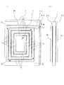
本発明の実施の形態のコイル部材を説明するために、図1(b)、(c)、(d)を用いるが、本発明はこの図に示されるコイル部材に限定されるものではない。図1(b)は、本発明の実施の形態のコイル部材を示す図であり、図1(c)は、図1(b)の側面図である。図1(d)は、図1(b)のコイル部の左上の二つのコーナ部分20の拡大図である。
【0026】
本発明の実施の形態のコイル部材は、絶縁基板1面上に延伸するコイル部3を具える。図1(b)、(c)には、コイル部3を他の部材と配線するための配線部4、裏面のコイル(不図示)と接続するための導通部5を含めたコイル線が示されている。このコイル線は、基板1面上に形成された導電膜2の上に導電膜2と同じ位置に電鋳法で形成された金属膜(以下電鋳膜と呼ぶ)で構成される。
【0027】
本発明の実施の形態のコイル部材のコイル部3を構成する電鋳膜の材料としては銅が好ましい。
【0028】
本発明の実施の形態のコイル部材が最も発明の効果を発揮するコイル部3の幅wは0.3mm以上、1.0mm以下である。
【0029】
本発明の実施の形態のコイル部材は、コイル部3がその幅wに対して高さ(厚み)hが同等以上の断面形状を有する場合に、特に発明の効果を発揮する。
【0030】
図1(b)を参照して本発明の実施の形態のコイル部材のコイル部3を説明すると、本発明のコイル部材19のコイル部3はコーナ部分20と非コーナ部分22とを有する。非コーナ部分22は直線状又は緩やかな曲線状に延伸する。前記非コーナ部分22がその延伸する方向を急激に変える部分がコーナ部分20である。コーナ部分20の長さは非コーナ部分22の長さと較べて短い。これら非コーナ部分22の複数は、本発明のコイル部材19のコイル部のコイルパターンの大枠を決める。
【0031】
図1(b)に示されたコイルパターンを説明する。このコイルパターンはほぼ矩形状で且つスパイラル状であり、7箇所のコーナ部分20と8箇所の非コーナ部分22とから構成されている。これら8箇所の非コーナ部分22が、大枠的に、ほぼ矩形状で且つスパイラル状のコイルパターンを形成している。一般に、本発明のコイル部材のコイルパターンは、コーナ部分の数をnとすると、非コーナ部分の数はn+1となる。
【0032】
本発明のコイル部材のコイル部のコイルパターンのコーナ部分の数は特に限定されず、又、巻数にも制限がない。又、コイルパターンはスパイラル状に限定されるものではない。
(内角条件)
本発明の実施の形態のコイル部材のコイル部3のコーナ部分の内角は、90度以上、180度未満であることが好ましい。ここで、内角とは、コイル部3が、一つの非コーナ部分22から、前記非コーナ部分22に隣接するコーナ部分20で急激に延伸の向きを変えて折れ曲がり、前記コーナ部分20に隣接する他の非コーナ部分22へ延伸するときに、前記二つの非コーナ部分がなす角、即ちコイル部の内角を意味する。具体的に、ほぼ直線状に延伸していたコイル部がコーナ部分で前記延伸方向に対して30度折れ曲がれば、内角は、180度−30度=150度から、150度である。
【0033】
上記内角の条件を充たすことにより、本発明の実施の形態のコイル部材のコイル部3のコーナ部分に於ける断面積欠損率を25%未満にすることができる。
【0034】
ここで、断面積欠損率は、コイル欠損部分に於いて減少したコイル部の断面積dの、コイル欠損がないときのコイル部の断面積Sに対する割合である。ここで図7(b)に示すように内角が90度のコーナ部分の場合、コイル欠損が無い場合の断面は長方形の部分、コイル欠損部分は、斜線で示した部分である。コイル部のその部分の線幅をw´、厚みをhとすると、断面積欠損率は次式で定義される。
断面積欠損率={d/(w´h)}×100(%)
本発明の実施の形態のコイル部材は、前記内角条件を充たすことに加えて、コイル部のコーナ部分に於ける折れ曲がりの頂点に当たる部分を角状に尖らせるのではなく、コーナ部分を全体として滑らかな曲線状にすることもできる。このコーナ部分の曲線の最小曲率半径は、以下に示す曲率半径条件を充たすことがより好ましい。
【0035】
曲線の曲率半径は、曲線が円弧状であれば曲線上の位置に依存せず一定であるので、円弧の半径が最小曲率半径である。円弧以外では曲線上の位置により曲率半径が変化する。その場合には、コーナ部分の最も小さい曲率半径を最小曲率半径とする。一般に曲線状のコーナ部分に於いて、曲率半径はコイル部の内側と外側の両方について定義できる。上記最小曲率半径はコイル部の内側についての値となる。今、コーナ部分に於ける最小曲率半径をrで表すと、rを大きくするほどコーナ部分に於ける断面積欠損率は小さくなる。しかしながら、大きくし過ぎると、そのコイル部材が発生する磁束の空間分布が、好ましい空間分布から大きく外れてしまうので、好ましくなく、断面積欠損率と磁束の空間分布とのトレードオフで決められる。
【0036】
本発明の実施の形態のコイル部材のコイル部のコーナ部分に於ける最小曲率半径rの条件は、コイル幅wに対して次式で与えられる。
(曲率半径条件) r≧1.5w(2w≧1mmのとき)
r≧1mm (2w<1mmのとき)
ここで、rはコーナ部分に於ける最小曲率半径、wはその部分に於けるコイル部の線幅である。
【0037】
前に述べたように、この曲率半径条件は、コーナ部分の形状が滑らかな曲線状であれば、円弧状に限定されない。円弧状、多次曲線状、どのような形状の曲線であっても、前記内角条件を充たし、その曲線の最小曲率半径が前記曲率半径条件を充たしていれば良い。
【0038】
このように前記曲率半径条件を、前記内角条件と合わせ充たすことにより、更に断面積欠損率を低減することができる。
【0039】
また、本発明の実施の形態のコイル部材は、コイル部のコーナ部分が上記の内角条件を充たすことに加えて、図8に示すように、コーナ部分20に角部21を複数持たせても良い。図8には一つのコーナ部分20に角部21が2箇所示される。
【0040】
そして、図8に示すように、この角部21を複数持ったコーナ部分20に内接する滑らかな曲線の最小曲率半径rを上記コーナ部分の最小曲率半径rとして上記曲率半径条件を適用することが好ましい。
【0041】
このような曲率半径条件を、内角条件と合わせ充たすことにより、本発明の実施形態のコイル部材はコイル部のコーナ部分に於ける断面積欠損率を更に低減することができる。
【0042】
本発明の実施の形態のコイル部材のコイル部のコイルパターンは、アンペアターンを大きくする為に、好ましくはスパイラル状にされる。図1に示された本発明の実施の形態のコイル部材には設けられていないが、アンペアターンを更に大きくする為に、絶縁性基板1の表面のみならず、裏面にもコイル部を配設することが好ましい。このとき、表面のコイル部3と裏面のコイル部(不図示)は導通部5で電気的に接続される。
【0043】
尚、コイル部3が延伸するコイルパターンがスパイラル状のときに、絶縁性基板1の単位面積当たりに配設されるコイル部3の巻数を出来るだけ多くする為に、又は、磁束を出来る限り効率的に発生させる為に、スパイラル状のコイル部3の隣接する線間の間隔は一定にされる。このとき、図1(d)に示すように、コイル部3の線幅をw1、コイル部3の隣接する線間の間隔をw2、内側のコイルの内周の曲率半径をr1としたときに、外側のコイル部の内周の曲率半径r2は、r2=r1+w1+w2の関係式から求められる。r2>r1であるので、通常、コイル部3の最内周の線の内側のコーナ部分の曲率半径が前記曲率半径条件を充たすように作製すれば、他の全てのコーナ部分の曲率半径条件は充たされる。
【0044】
本発明のコイル部材が、前記内角条件、又は前記曲率半径条件を充たすことにより、断面積欠損率が低減する理由を、図5、図6(a)、図6(b)、図6(c)を用いて以下に詳しく説明する。図6は、発明の理解を容易にするために、コイルパターンの巻数を1とし、片面のみにコイル部が形成される図とした。
【0045】
図5は本発明の実施の形態のコイル部材のコイル部を電鋳法により形成するための電鋳装置を示す概略図であり、従来の電鋳装置との違いはない。電鋳装置には電鋳槽9が設けられている。電鋳槽9の中には、電鋳液10が、液面が図示の波線部で一定になる量で満たされている。そして電鋳液10は電鋳槽9の外側側面に設けられた流出部11から溢れ出て、電鋳液10は、ポンプ13を介して吹き付け穴14よりコイル部材基板17に吹き付けられる。電鋳液10をコイル部材基板17に吹き付けることにより、電鋳膜は均一に成膜される。
【0046】
コイル部材基板17は、ワークホルダー16に固定され、この状態でワークホルダー16は、電鋳槽9の上方クロスバー15に吊り下げられる。この時、コイル部材基板17は、コイル部を形成する面が液面と電界方向の双方に対して、垂直になるよう、電鋳液10中に浸漬される。このコイル部材基板17は、前述のコイル部材製造プロセスに於ける▲2▼で説明したように、予めレジストパターニングが終了し、電鋳膜の不必要な部分はマスキングされている。
【0047】
コイル部材基板17は、ワークホルダー16及びクロスバー15を介して接地電位にされ、その左右両側にアノード18が配設されて、アノード18が所定電位となるよう電源が供給されている。従って、コイル部材基板17の左側の導電膜の面と左のアノード18との間と、コイル部材基板17の右側の導電膜の面と右のアノード18との間の両方に電界が発生する。これにより電鋳膜が基板1の左右のスパイラル状の導電膜パターン上に成長して、コイル部材が作製される。
【0048】
ところが、従来のコイル部材では、コーナ部分での断面積欠損率が高かった。
【0049】
この理由を、発明者は以下のように推定している。
【0050】
電鋳液10中には液の循環など何らかの理由でガス(例えば空気)が取り込まれる。電鋳液10中に取り込まれたガスは、吹き付け穴14を通ってコイル部材基板17へ吹き付けられ、気泡となってレジストパターンの隙間に入り込む。この時の気泡のサイズは、レジストパターンの隙間に比して小さいので、容易にその隙間に入り込む。隙間に入り込んだ気泡は、浮力により液面方向に向かい、その大半は液面を出て大気へ放出されるが、中には、図6(a)に示すように、レジストパターンのコーナ部に集まって、大きな気泡7となり滞留するものがある。この気泡7の滞留は長時間に及び、その気泡7が入り込んだ部分だけ電鋳膜の成膜が阻害される為に、図6(b)に示すような電鋳膜のコイル欠損8を招いていたものと推定される。
【0051】
図6(c)は、気泡7がレジスト膜6のコーナ部分に集まり、留まる様子を詳細に説明する拡大図である。レジストを電鋳液に浸漬すると、レジストが膨潤することにより、コーナ部分20の内側は鋭角になる。コーナ部分が鋭角であり、レジストの隙間(溝)が深いと、気泡に働く浮力の関係で、気泡が鋭角のコーナ部分に挟み込まれる形になるために、気泡が滞留し易くなる。前述のように、気泡が滞留した部分では電鋳膜の成長が阻害される為に、電鋳膜のコイル欠損を招いていたものと推定される。
【0052】
本発明の実施の形態のコイル部材は、図1(b)、図2(a)、又は図2(b)に示されるように、コイルパターンのコーナ部分において、前述の内角条件を充たし、又は、前述内角条件に加えてコーナ部分の最小曲率半径が前述の曲率半径条件を充たしている。そのために、気泡がコーナ部分に挟み込まれることがない。仮に挟み込まれても容易にレジストパターンの隙間から遊離するので、気泡の滞留が少なく、コイル部の断面積欠損が小さく且つ少ない。
【0053】
本発明の実施の形態のコイル部材は、製造工程においてレジストパターンを、前記内角条件を充たすか、又は前記内角条件と前記曲率半径条件の両方を充たすコイルパターンの反転パターンにすれば、コイル欠損が小さく且つ少なくなる。その為に、レジストパターニング工程において、マスクパターンを変更するだけで達成されるので、容易に実施することができる。従来の電鋳装置や従来の電鋳方法をそのまま用いることができ、装置の改造や電鋳方法の改善は不要である。
【0054】
また、本発明の実施の形態のコイル部材は量産に向いた電鋳法で製造できるので、低コストである。
[実施例1]
図1(a)、(b)、(c)、(d)は、実施例1のコイル部材を説明する図である。図1(b)は、コイルパターンを示す図、図1(c)は、図1(b)の側面図である。図1(d)は、図1(b)のコーナ部分20の拡大図である。図1(a)は、本実施例のコイル部材を作製するために用いられるレジストのレジストパターンを示す。
【0055】
本実施例のコイル部材は絶縁基板1と、前記絶縁性基板1面上に配設された、コイル部3と、前記コイル部3を他の部材(不図示)と配線するための配線部4と、表面のコイル部3と裏面のコイル部(不図示)と接続するための導通部5を具える。コイル部3と配線部4と導通部5とから成るコイル線は基板1面上に形成された導電膜2の上に電鋳法で形成された銅の電鋳膜で構成され、7箇所のコーナ部20と8箇所の非コーナ部とを具える。
【0056】
コイル線のコイルパターンは発明を明確にするために簡略化されたスパイラル状で、且つ矩形状とされている。コイル線の線幅wは0.6mm、コイル線の厚みも0.6mmで、コイル線の断面形状は正方形である。
【0057】
コーナ部分20の内角は90度とされている。90度は内角条件の限界値であるが、合わせてコーナ部分の形状を円弧状とし、その曲率半径が曲率半径条件を満足するように設計することにより断面積欠損率を低減させた。即ち最小曲率半径である最内周の曲率半径r1をコイル幅w=w1=0.6mmの4倍の2.4mmと充分に大きくした。
【0058】
本実施例の場合、コイル線の幅、コイル線の間隙とも一様になっているので、スパイラルコイル線の間隙w2を0.3mmとすれば、一つ外側のコーナ部分の曲率半径r2は、r2=r1+w1+w2=3.3mmから、3.3mmとなる。ここでは、コイルの巻数を2としたが、巻数が2を超えるコイル部材でも、同様にして曲率半径を決定すれば良い。
【0059】
次に、本実施例のコイル部材のコイル線の製造プロセスを図1、図4を参照して説明する。
▲1▼250mm×140mm×2mmtの石英ガラス基板1表面上に導電膜2として銅膜をスパッタ法で形成した。
▲2▼約50μm厚のシート状レジストであるネガ型レジスト(日立化成工業製、日立感光性フィルム PHOTEC H−6250EA)を13層、導電膜上に以下のラミネート条件でラミネータ(日立高温ラミネータHLM−3000)を通すことにより積層し、約0.65mmのレジスト膜を形成した。
【0060】
ロール温度:110℃±1℃
ロール圧力:0.4MPa
ラミネート速度:2m/分
次に、図1(b)のコイルパターンの反転形状を有する、レジストパターン用のフィルム状マスクを作製した。このとき、電鋳工程でレジスト膜が膨潤してレジストパターンが変形することを予め考慮して、コイルパターンのコーナ部分に対応するレジストパターン形成用のマスクのコーナ部分の内角を、作製対象のコイル部材のコイルパターンのコーナ部分の内角よりも大きめに補正した。このマスクを使用し、両面露光機(オーク社製、HMW−201GX)を用い、ST=23/41段 ステップタブレットの露光条件で、レジスト膜を露光した。その後、アルカリ型自動現像機で現像液としてNa2CO3の1wt%の水溶液を用い、30℃、0.2MPaの圧力でレジスト膜に吹き付け、図1(a)のレジストパターンを形成した。
▲3▼図5に示された電鋳装置を用い、銅電鋳法により、石英基板上のレジスト膜が除去された部分に銅膜3を厚み0.6mm形成した。銅メッキ浴として硫酸銅浴を用いた。
▲4▼銅膜を電鋳後、40℃のNaOHの5wt%水溶液に浸漬し、レジスト膜を剥離した。
▲5▼▲4▼で剥離したレジスト膜の下の導電膜を剥離した。
▲6▼最後に、絶縁性基板を洗浄し、コイル部材1を完成させた。
【0061】
これにより、気泡の滞留を確実に無くすことができ、断面積欠損率を大幅に減らすことができた。
[実施例2]
図2(a)は、実施例2のコイル部材を説明する図であり、コイルパターンの平面図を示し、図8はコーナ部分の拡大図を示す。
【0062】
本実施例のコイル部材の実施例1との違いは、コイル線がコーナ部分20を3箇所、非コーナ部分22を4箇所持ち、各コーナ部分20が2箇所の角部21を持ち、コイル線のコイルパターンが、発明を明確にするために、巻数が1のスパイラル状とされている点である。
【0063】
尚、角部を1箇所設ければコイル線の内側と外側に1箇所づつ計2箇所の対応場所が生じる。
【0064】
コーナ部分20の内角は90度であり、コーナ部分20は角部21を2箇所用いてコイル部の延伸方向を90度変えるようされ、且つ、図2(a)に示すコイル線の左上のコーナ部20のコイル線の内側の拡大図図8に示すように、コーナ部分に内接する曲線の最小曲率半径rを線幅の4倍の2.4mmとした。
【0065】
このような構成にすることにより、本実施例のコイル部材は製造中に気泡の滞留を確実に無くすことができ、断面積欠損率を大幅に減らすことができた。
[実施例3]
図2(b)は、実施例3のコイル部材を説明する図であり、コイルパターンの平面図を示す。
【0066】
本実施例のコイル部材の実施例2との違いは、各コーナ部分20が4箇所の角部21を持っている点である。
【0067】
コーナ部分20の内角は90度であり、コーナ部分20は角部21を4箇所用いてコイル部の延伸方向を90度変えるようにされ、且つ、コーナ部分に内接する曲線の最小曲率半径を線幅の4倍の2.4mmとした。
【0068】
このような構成にすることにより、気泡の滞留を確実に無くすことができ、断面積欠損率を大幅に減らすことができた。
【0069】
【発明の効果】
本発明のコイル部材は、コイル部の断面積欠損率が低いために、低コストで高性能である。
【図面の簡単な説明】
【図1】本発明の実施の形態又は実施例1のコイル部材を説明する図である。
【図2】(a)は本発明の実施例2の、(b)は実施例3のコイル部材を説明する図である。
【図3】コイル部材を説明する図である。
【図4】電鋳によるコイル部材製造のフローである。
【図5】電鋳装置の概要を示す。
【図6】従来のコイル部材の体積欠損の発生メカニズムを説明する図である。
【図7】断面積欠損率の定義を説明する図である。
【図8】複数の角部を持つコーナ部とこのコーナ部に内接する曲線と曲率半径rとを示す。
【符号の説明】
1 絶縁性基板
2、2a、2b 導電膜
3、3a、3b コイル部
4、4a、4b 配線部
5 導通部
6 レジスト膜
7 気泡
8 電鋳膜の欠損部
9 電鋳槽
10 電鋳液
11 流出部
13 ポンプ
14 吹き付け穴
15 クロスバー
16 ワーク(コイル部材基板)ホルダー
17 コイル部材基板
18 アノード
19 コイル部材
20 コーナ部分
21 角部
22 非コーナ部分[0001]
TECHNICAL FIELD OF THE INVENTION
The present invention relates to an electric coil member formed on a substrate surface by an electroforming method and used for a magnetic field generator for deflecting a charged particle beam.
[0002]
[Prior art]
2. Description of the Related Art Conventionally, in a coil member including a coil wire having a rectangular cross section and extending in a desired pattern on a thin substrate surface such as ceramic, the coil wire is manufactured by a wire electric discharge machining method. Then, the coil member is manufactured by bonding the coil wire to an accurate position on the substrate surface.
[0003]
However, when the number of turns of the coil wire is increased, the electric discharge machining time increases. Further, since the coil wire has a spring property and is easily elastically deformed, it is difficult to bond the coil wire to a precise position on the substrate, and the bonding time is increased. Therefore, the manufacturing cost of the coil member was high.
[0004]
Therefore, a low-cost coil member has been desired.
[0005]
By the way, it is known that the electroforming method can easily and inexpensively form a thick conductive film necessary for flowing a desired current through a coil wire. Then, in order to solve the above-mentioned problems, a technology for producing a coil wire by an electroforming method has been developed.
[0006]
This technology forms a thin conductive film on the substrate surface, applies a photoresist on it, exposes the formed resist film to a mask pattern, and develops it. To form a coil member by forming an electroformed film of metal. (For example, refer to
[0007]
[Patent Document 1]
JP 2001-210540 A
[0008]
[Problems to be solved by the invention]
FIGS. 3A and 3B show an example of a coil member having a coil wire formed on a substrate surface by an electroforming method. 3 (a) and 3 (b),
[0009]
In this example, coil portions are provided on both surfaces of the
[0010]
The
[0011]
Since the width and height of the
[0012]
Next, the direction of the current flowing through the coil wire is indicated by an arrow in FIG. When a current flows from one end of the coil wire, that is, from the wiring portion 4a, a current flows toward the inside of the spiral of the
[0013]
The manufacturing process of the coil member shown in FIG. 3 will be described with reference to FIG.
{Circle around (1)} First, conductive films 2a and 2b are formed on substantially the entire surfaces of both surfaces of the
{Circle around (2)} A resist film is formed by applying a negative photoresist resin, pattern exposure is performed, and then development is performed to form a resist pattern having an inverted shape of a desired coil pattern. The conductive film is insulated at the resist pattern portion and has conductivity at the portion where the resist film is removed. The shape of the portion from which the resist film has been removed is the same spiral shape as the desired coil pattern shape. At this time, the thickness of the resist film is set to be larger than a desired thickness (height) of the coil wire.
(3) Copper
(4) After forming the copper electroformed film to a desired thickness, the resist film is removed.
(5) The conductive film under the resist film removed in (4) is removed by etching.
{Circle around (6)} Finally, if the insulating substrate is washed, a coil member having a coil wire having a desired thickness (height) with a desired spiral coil pattern is completed.
[0014]
However, in the coil member manufactured in this manner, the problem that the coil wire is largely lost at the corner portion has frequently occurred. FIG. 6B is a diagram showing a state of the coil wire being lost. In FIG. 6B,
[0015]
This coil loss reduces the volume of the coil wire. As a result, since the resistance value of the coil circuit increases, the maximum current that can be passed through the coil wire decreases, and the performance of the coil member significantly decreases. Therefore, the production yield was low and the production cost was high.
[0016]
An object of the present invention is to provide a low-cost, high-performance coil member that solves the above-described problem, has a small coil loss, and has a low defect ratio in a cross section of the coil (hereinafter, referred to as a cross-sectional defect ratio). .
[0017]
[Means for solving the problem]
In order to solve the above problems, a coil member according to a first aspect of the present invention is a coil member including a coil portion extending in a desired pattern on a substrate surface, wherein the coil portion is formed by an electroforming method. Wherein the pattern has a corner portion, and a cross-sectional area defect rate of the coil portion at the corner portion is less than 25%.
[0018]
Here, the corner portion means a portion where a coil extending in a straight line or a gently curved shape on the substrate surface sharply changes the extending direction. The cross-sectional area defect rate indicates the reduction rate of the actual cross-sectional area with respect to the design value of the cross-sectional area in a cross section perpendicular to the direction in which the coil portion extends.
[0019]
The coil member according to the second aspect of the present invention, in the coil member according to the first aspect, wherein the pattern is a straight line or a non-corner portion extending in a gently curved shape and the non-corner portion sharply extends from the non-corner portion. And a corner portion that changes the stretching direction, and an angle between two non-corner portions sandwiching the corner portion is more than 90 degrees and less than 180 degrees.
[0020]
A coil member according to a third aspect of the present invention is the coil member according to the second aspect, wherein the shape of the corner portion is a smooth curve, and the minimum radius of curvature of the curve is given by the following equation: It is.
[0021]
r ≧ 1.5w (when 2w ≧ 1mm)
r ≧ 1mm (when 2w <1mm)
Here, r is the minimum radius of curvature at the corner portion, and w is the line width of the coil portion at that portion.
[0022]
The coil member according to a fourth aspect of the present invention is the coil member according to the second aspect, wherein the corner portion has a plurality of corners, and the minimum radius of curvature of a smooth curve inscribed in the corner portion is as follows. It is given by the formula.
[0023]
r ≧ 1.5w (when 2w ≧ 1mm)
r ≧ 1mm (when 2w <1mm)
Here, r is the minimum radius of curvature at the corner portion, and w is the line width of the coil portion at that portion.
[0024]
A coil member according to a fifth aspect of the present invention is the coil member according to the second aspect, wherein the corner portion is formed by a curve.
[0025]
BEST MODE FOR CARRYING OUT THE INVENTION
[Embodiment of the invention]
1 (b), 1 (c) and 1 (d) are used to describe a coil member according to an embodiment of the present invention, but the present invention is not limited to the coil member shown in this figure. FIG. 1B is a diagram showing a coil member according to the embodiment of the present invention, and FIG. 1C is a side view of FIG. 1B. FIG. 1D is an enlarged view of two upper
[0026]
The coil member according to the embodiment of the present invention includes a
[0027]
Copper is preferable as the material of the electroformed film forming the
[0028]
The width w of the
[0029]
The coil member according to the embodiment of the present invention exerts the effects of the invention particularly when the
[0030]
The
[0031]
The coil pattern shown in FIG. 1B will be described. This coil pattern has a substantially rectangular shape and a spiral shape, and includes seven
[0032]
The number of corner portions of the coil pattern of the coil portion of the coil member of the present invention is not particularly limited, and the number of turns is not limited. Further, the coil pattern is not limited to a spiral shape.
(Internal angle condition)
It is preferable that the inner angle of the corner portion of the
[0033]
By satisfying the condition of the interior angle, the cross-sectional area defect rate at the corner portion of the
[0034]
Here, the cross-sectional area defect rate is a ratio of the reduced cross-sectional area d of the coil portion in the coil defective portion to the cross-sectional area S of the coil portion when there is no coil defect. Here, as shown in FIG. 7B, in the case of a corner portion having an inner angle of 90 degrees, the cross section when there is no coil loss is a rectangular portion, and the coil loss portion is a portion indicated by oblique lines. Assuming that the line width of the coil portion is w 'and the thickness is h, the sectional area defect rate is defined by the following equation.
Cross-sectional area defect rate = {d / (w'h)} x 100 (%)
The coil member according to the embodiment of the present invention, in addition to satisfying the internal angle condition, does not sharpen the portion corresponding to the apex of the bend at the corner portion of the coil portion, but smoothes the corner portion as a whole. It can also be a curved shape. More preferably, the minimum radius of curvature of the curve in the corner portion satisfies the following radius of curvature condition.
[0035]
If the radius of curvature of the curve is a circular arc, the radius of the arc is the minimum radius of curvature since the radius of the arc is constant regardless of the position on the curve. Outside the arc, the radius of curvature changes depending on the position on the curve. In this case, the smallest radius of curvature of the corner portion is set as the minimum radius of curvature. Generally, in a curved corner portion, the radius of curvature can be defined both inside and outside the coil portion. The minimum radius of curvature is a value for the inside of the coil portion. Now, if the minimum radius of curvature at the corner portion is represented by r, the larger the value of r, the smaller the cross-sectional area defect rate at the corner portion. However, if it is too large, the spatial distribution of the magnetic flux generated by the coil member greatly deviates from the preferable spatial distribution.
[0036]
The condition of the minimum radius of curvature r at the corner of the coil portion of the coil member according to the embodiment of the present invention is given by the following equation with respect to the coil width w.
(Curvature radius condition) r ≧ 1.5w (when 2w ≧ 1mm)
r ≧ 1mm (when 2w <1mm)
Here, r is the minimum radius of curvature at the corner portion, and w is the line width of the coil portion at that portion.
[0037]
As described above, the curvature radius condition is not limited to the arc shape as long as the shape of the corner portion is a smooth curved shape. Regardless of the shape of the curve, such as an arc, a multi-degree curve, or the like, it is sufficient that the above-mentioned interior angle condition is satisfied, and the minimum radius of curvature of the curve satisfies the above-mentioned radius of curvature condition.
[0038]
As described above, by satisfying the curvature radius condition and the interior angle condition, the sectional area defect rate can be further reduced.
[0039]
Further, in the coil member according to the embodiment of the present invention, in addition to the corner portion of the coil portion satisfying the above-described interior angle condition, as shown in FIG. 8, the
[0040]
Then, as shown in FIG. 8, the minimum radius of curvature r of the smooth curve inscribed in the
[0041]
By satisfying such a curvature radius condition and an interior angle condition, the coil member according to the embodiment of the present invention can further reduce the cross-sectional area defect rate at the corner portion of the coil portion.
[0042]
The coil pattern of the coil portion of the coil member according to the embodiment of the present invention is preferably formed in a spiral shape to increase the ampere turn. Although not provided in the coil member of the embodiment of the present invention shown in FIG. 1, a coil portion is provided not only on the front surface but also on the back surface of the insulating
[0043]
When the coil pattern in which the
[0044]
The reason why the coil member of the present invention satisfies the interior angle condition or the curvature radius condition to reduce the cross-sectional area defect rate is described with reference to FIGS. 5, 6A, 6B, and 6C. ) Will be described in detail below. FIG. 6 is a diagram in which the number of turns of the coil pattern is set to 1 and the coil portion is formed on only one side for easy understanding of the invention.
[0045]
FIG. 5 is a schematic view showing an electroforming apparatus for forming the coil portion of the coil member according to the embodiment of the present invention by an electroforming method, and there is no difference from the conventional electroforming apparatus. The electroforming apparatus is provided with an electroforming tank 9. The electroforming tank 9 is filled with the electroforming liquid 10 in such an amount that the liquid level becomes constant at the wavy line shown in the figure. Then, the electroforming liquid 10 overflows from an outflow portion 11 provided on the outer side surface of the electroforming tank 9, and the electroforming liquid 10 is blown to the coil member substrate 17 from a blowing hole 14 via a pump 13. By spraying the electroforming liquid 10 onto the coil member substrate 17, the electroforming film is formed uniformly.
[0046]
The coil member substrate 17 is fixed to the work holder 16, and in this state, the work holder 16 is suspended from the upper cross bar 15 of the electroforming tank 9. At this time, the coil member substrate 17 is immersed in the electroforming liquid 10 such that the surface forming the coil portion is perpendicular to both the liquid surface and the direction of the electric field. As described in (2) in the coil member manufacturing process, the coil member substrate 17 has been subjected to resist patterning in advance, and unnecessary portions of the electroformed film are masked.
[0047]
The coil member substrate 17 is set to a ground potential via the work holder 16 and the cross bar 15, and anodes 18 are provided on both left and right sides thereof, and power is supplied so that the anode 18 has a predetermined potential. Therefore, an electric field is generated both between the left conductive film surface of the coil member substrate 17 and the left anode 18 and between the right conductive film surface and the right anode 18 of the coil member substrate 17. Thus, the electroformed film grows on the left and right spiral conductive film patterns of the
[0048]
However, in the conventional coil member, the cross-sectional area defect rate at the corner portion was high.
[0049]
The inventors presume the reason for this as follows.
[0050]
Gas (for example, air) is taken into the electroforming liquid 10 for some reason such as circulation of the liquid. The gas taken into the electroforming liquid 10 is blown to the coil member substrate 17 through the blowing holes 14 to form bubbles and enter the gaps of the resist pattern. Since the size of the bubbles at this time is smaller than the gap between the resist patterns, the bubbles easily enter the gap. Bubbles that have entered the gap move toward the liquid surface due to buoyancy, and most of the bubbles exit the liquid surface and are released to the atmosphere. However, as shown in FIG. Some gather and become
[0051]
FIG. 6C is an enlarged view for explaining in detail the manner in which bubbles 7 collect and stay at the corners of the resist
[0052]
As shown in FIG. 1 (b), FIG. 2 (a), or FIG. 2 (b), the coil member according to the embodiment of the present invention satisfies the above-described interior angle condition at a corner portion of the coil pattern. In addition to the above-described interior angle condition, the minimum radius of curvature of the corner portion satisfies the above-described radius of curvature condition. Therefore, bubbles are not trapped in the corner portions. Even if it is interposed, it is easily released from the gap between the resist patterns, so that the retention of bubbles is small, and the cross-sectional area defect of the coil portion is small and small.
[0053]
In the coil member according to the embodiment of the present invention, if the resist pattern in the manufacturing process satisfies the internal angle condition, or is an inverted pattern of the coil pattern that satisfies both the internal angle condition and the radius of curvature condition, a coil defect may occur. Smaller and less. Therefore, in the resist patterning step, this can be achieved simply by changing the mask pattern, so that it can be easily implemented. The conventional electroforming apparatus and the conventional electroforming method can be used as they are, and there is no need to modify the apparatus or to improve the electroforming method.
[0054]
Further, the coil member according to the embodiment of the present invention can be manufactured by an electroforming method suitable for mass production, so that the cost is low.
[Example 1]
1A, 1B, 1C, and 1D are diagrams illustrating a coil member according to the first embodiment. FIG. 1B is a diagram showing a coil pattern, and FIG. 1C is a side view of FIG. 1B. FIG. 1D is an enlarged view of the
[0055]
The coil member according to the present embodiment includes an insulating
[0056]
The coil pattern of the coil wire has a simplified spiral shape and rectangular shape for clarity of the invention. The wire width w of the coil wire is 0.6 mm, the thickness of the coil wire is 0.6 mm, and the cross-sectional shape of the coil wire is square.
[0057]
The inner angle of the
[0058]
In the case of the present embodiment, since the width of the coil wire and the gap between the coil wires are also uniform, if the gap w2 between the spiral coil wires is 0.3 mm, the radius of curvature r2 of the outer corner portion is: r2 = r1 + w1 + w2 = 3.3 mm from 3.3 mm Here, the number of turns of the coil is two, but the radius of curvature may be determined in the same manner for a coil member having more than two turns.
[0059]
Next, a manufacturing process of the coil wire of the coil member of the present embodiment will be described with reference to FIGS.
(1) 250mm x 140mm x 2mm t A copper film was formed as a
(2) A laminator (Hitachi High Temperature Laminator HLM-) having 13 layers of a negative resist (Hitachi Kasei Kogyo Co., Ltd., Hitachi Photosensitive Film PHOTEC H-6250EA), which is a sheet-like resist having a thickness of about 50 μm, is laminated on the conductive film under the following laminating conditions. 3000) to form a resist film of about 0.65 mm.
[0060]
Roll temperature: 110 ° C ± 1 ° C
Roll pressure: 0.4 MPa
Laminating speed: 2m / min
Next, a film-shaped mask for a resist pattern having an inverted shape of the coil pattern of FIG. 1B was prepared. At this time, considering in advance that the resist film swells and deforms the resist pattern in the electroforming process, the inner angle of the corner portion of the mask for forming the resist pattern corresponding to the corner portion of the coil pattern is set to the coil to be formed. The correction was made larger than the inner angle of the corner portion of the coil pattern of the member. Using this mask, a resist film was exposed using a double-sided exposure machine (manufactured by Oak Co., HMW-201GX) under the exposure conditions of a ST = 23/41 step tablet. Thereafter, Na was used as a developing solution in an alkaline automatic developing machine. Two CO Three Was sprayed onto the resist film at 30 ° C. and a pressure of 0.2 MPa to form a resist pattern shown in FIG. 1A.
{Circle around (3)} Using the electroforming apparatus shown in FIG. 5, a
{Circle around (4)} After the copper film was electroformed, it was immersed in a 5 wt% aqueous solution of NaOH at 40 ° C. to remove the resist film.
The conductive film under the resist film peeled in (5) and (4) was peeled off.
{Circle around (6)} Finally, the insulating substrate was washed to complete the
[0061]
As a result, the stagnation of air bubbles could be reliably eliminated, and the cross-sectional area defect rate could be significantly reduced.
[Example 2]
FIG. 2A is a view for explaining a coil member of Example 2, and shows a plan view of a coil pattern, and FIG. 8 shows an enlarged view of a corner portion.
[0062]
The difference between the coil member of the present embodiment and the first embodiment is that the coil wire has three
[0063]
In addition, if one corner is provided, a total of two corresponding locations will be generated, one inside and one outside the coil wire.
[0064]
The inner angle of the
[0065]
By adopting such a configuration, the coil member of the present example was able to surely eliminate the stagnation of air bubbles during manufacturing, and was able to significantly reduce the cross-sectional area defect rate.
[Example 3]
FIG. 2B is a diagram illustrating a coil member according to the third embodiment, and shows a plan view of a coil pattern.
[0066]
The difference of the coil member of the present embodiment from that of the second embodiment is that each
[0067]
The interior angle of the
[0068]
With such a configuration, the stagnation of bubbles can be reliably eliminated, and the cross-sectional area defect rate can be significantly reduced.
[0069]
【The invention's effect】
The coil member of the present invention has low cost and high performance because the sectional area defect rate of the coil portion is low.
[Brief description of the drawings]
FIG. 1 is a diagram illustrating a coil member according to an embodiment or an example 1 of the present invention.
FIG. 2A is a diagram illustrating a coil member according to a second embodiment of the present invention, and FIG. 2B is a diagram illustrating a coil member according to a third embodiment.
FIG. 3 is a diagram illustrating a coil member.
FIG. 4 is a flowchart of manufacturing a coil member by electroforming.
FIG. 5 shows an outline of an electroforming apparatus.
FIG. 6 is a diagram illustrating a mechanism of generating a volume defect of a conventional coil member.
FIG. 7 is a diagram illustrating a definition of a cross-sectional area defect rate.
FIG. 8 shows a corner having a plurality of corners, a curve inscribed in the corner, and a radius of curvature r.
[Explanation of symbols]
1 Insulating substrate
2, 2a, 2b conductive film
3, 3a, 3b Coil section
4, 4a, 4b wiring section
5 Conducting part
6 Resist film
7 bubbles
8 Defects in electroformed film
9 Electroforming tank
10 Electroforming liquid
11 Outflow
13 pump
14 Spray hole
15 Crossbar
16 Work (coil member substrate) holder
17 Coil member substrate
18 Anode
19 Coil member
20 corners
21 corner
22 Non-corner part
Claims (5)
r≧1.5w(2w≧1mmのとき)
r≧1mm (2w<1mmのとき)
ここで、rはコーナ部分に於ける最小曲率半径、wはその部分に於けるコイル部の線幅である。The coil member according to claim 2, wherein the shape of the corner portion is a smooth curve, and the minimum radius of curvature of the curve is given by the following equation.
r ≧ 1.5w (when 2w ≧ 1mm)
r ≧ 1mm (when 2w <1mm)
Here, r is the minimum radius of curvature at the corner portion, and w is the line width of the coil portion at that portion.
r≧1.5w(2w≧1mmのとき)
r≧1mm (2w<1mmのとき)
ここで、rはコーナ部分に於ける最小曲率半径、wはその部分に於けるコイル部の線幅である。The coil member according to claim 2, wherein the corner portion has a plurality of corners, and a minimum radius of curvature of a smooth curve inscribed in the corner portion is given by the following equation.
r ≧ 1.5w (when 2w ≧ 1mm)
r ≧ 1mm (when 2w <1mm)
Here, r is the minimum radius of curvature at the corner portion, and w is the line width of the coil portion at that portion.
Priority Applications (1)
| Application Number | Priority Date | Filing Date | Title |
|---|---|---|---|
| JP2002367163A JP2004200406A (en) | 2002-12-18 | 2002-12-18 | Coil member |
Applications Claiming Priority (1)
| Application Number | Priority Date | Filing Date | Title |
|---|---|---|---|
| JP2002367163A JP2004200406A (en) | 2002-12-18 | 2002-12-18 | Coil member |
Publications (1)
| Publication Number | Publication Date |
|---|---|
| JP2004200406A true JP2004200406A (en) | 2004-07-15 |
Family
ID=32764147
Family Applications (1)
| Application Number | Title | Priority Date | Filing Date |
|---|---|---|---|
| JP2002367163A Withdrawn JP2004200406A (en) | 2002-12-18 | 2002-12-18 | Coil member |
Country Status (1)
| Country | Link |
|---|---|
| JP (1) | JP2004200406A (en) |
Cited By (6)
| Publication number | Priority date | Publication date | Assignee | Title |
|---|---|---|---|---|
| JP2008252121A (en) * | 2008-06-09 | 2008-10-16 | Tdk Corp | Common mode choke coil |
| JP2010129985A (en) * | 2008-12-01 | 2010-06-10 | Nichia Corp | Semiconductor device |
| KR20180006247A (en) | 2016-07-07 | 2018-01-17 | 삼성전기주식회사 | Coil component |
| JP2019016622A (en) * | 2017-07-03 | 2019-01-31 | 太陽誘電株式会社 | Coil component |
| US10923259B2 (en) | 2016-07-07 | 2021-02-16 | Samsung Electro-Mechanics Co., Ltd. | Coil component |
| WO2022220617A1 (en) * | 2021-04-15 | 2022-10-20 | 엘지이노텍 주식회사 | Camera actuator, and camera device and optical device comprising same |
-
2002
- 2002-12-18 JP JP2002367163A patent/JP2004200406A/en not_active Withdrawn
Cited By (9)
| Publication number | Priority date | Publication date | Assignee | Title |
|---|---|---|---|---|
| JP2008252121A (en) * | 2008-06-09 | 2008-10-16 | Tdk Corp | Common mode choke coil |
| JP2010129985A (en) * | 2008-12-01 | 2010-06-10 | Nichia Corp | Semiconductor device |
| KR20180006247A (en) | 2016-07-07 | 2018-01-17 | 삼성전기주식회사 | Coil component |
| US10923259B2 (en) | 2016-07-07 | 2021-02-16 | Samsung Electro-Mechanics Co., Ltd. | Coil component |
| JP2019016622A (en) * | 2017-07-03 | 2019-01-31 | 太陽誘電株式会社 | Coil component |
| US11114229B2 (en) | 2017-07-03 | 2021-09-07 | Taiyo Yuden Co., Ltd. | Coil component |
| JP7015650B2 (en) | 2017-07-03 | 2022-02-03 | 太陽誘電株式会社 | Coil parts |
| US11955276B2 (en) | 2017-07-03 | 2024-04-09 | Taiyo Yuden Co., Ltd. | Coil component |
| WO2022220617A1 (en) * | 2021-04-15 | 2022-10-20 | 엘지이노텍 주식회사 | Camera actuator, and camera device and optical device comprising same |
Similar Documents
| Publication | Publication Date | Title |
|---|---|---|
| US8597490B2 (en) | Method of manufacturing a gas electron multiplier | |
| US4374707A (en) | Orifice plate for ink jet printing machines | |
| KR102474454B1 (en) | Deposition mask manufacturing method and deposition mask | |
| KR100621550B1 (en) | Method for fabricating tape wiring substrate | |
| US20020027127A1 (en) | Method of manufacturing wireless suspension blank | |
| WO2004065660A1 (en) | Metal photo-etching product and production method therefor | |
| KR20180077075A (en) | Mask for vapor deposition and forming method and manufacturing method of the same | |
| KR102478473B1 (en) | Method of manufacturing mask for depositing | |
| JP2003273498A (en) | Method of manufacturing printed-wiring board | |
| JP2004200406A (en) | Coil member | |
| JP6366034B2 (en) | Lead frame for semiconductor device and manufacturing method thereof | |
| JPH10320736A (en) | Production of suspension element for magnetic head having wire pattern and its producing device | |
| KR100700660B1 (en) | Mask and method for fabricating thereof | |
| JP2004263218A (en) | Pattern plating method | |
| JP2007111942A (en) | Metal mask and its manufacturing method | |
| JP2017137582A (en) | Metal mask with resin layer | |
| CN219609434U (en) | Photomask for preparing metal mask plate | |
| KR101786548B1 (en) | Metal mask for fabrication of OLED and its manufacturing method | |
| JP2992647B2 (en) | Method for producing electroformed product having through-hole | |
| JPH0590475A (en) | Lead frame and manufacture thereof | |
| CN112186103B (en) | Resistor structure and manufacturing method thereof | |
| CN116994948B (en) | Chip electrode preparation method and semiconductor device | |
| JP2005181699A (en) | Method for manufacturing fine projection array, fine projection array, fine recessed surface array, and method for manufacturing fine recessed surface array | |
| JP2013170301A (en) | Method for producing vapor deposition mask | |
| JP2008153391A (en) | Circuit board and manufacturing method therefor |
Legal Events
| Date | Code | Title | Description |
|---|---|---|---|
| A300 | Withdrawal of application because of no request for examination |
Free format text: JAPANESE INTERMEDIATE CODE: A300 Effective date: 20060307 |