JP2004179327A - Alloy material for semiconductor, semiconductor chip using the same and method for manufacturing semiconductor chip - Google Patents
Alloy material for semiconductor, semiconductor chip using the same and method for manufacturing semiconductor chip Download PDFInfo
- Publication number
- JP2004179327A JP2004179327A JP2002342797A JP2002342797A JP2004179327A JP 2004179327 A JP2004179327 A JP 2004179327A JP 2002342797 A JP2002342797 A JP 2002342797A JP 2002342797 A JP2002342797 A JP 2002342797A JP 2004179327 A JP2004179327 A JP 2004179327A
- Authority
- JP
- Japan
- Prior art keywords
- film
- alloy material
- semiconductor
- alloy
- semiconductor chip
- Prior art date
- Legal status (The legal status is an assumption and is not a legal conclusion. Google has not performed a legal analysis and makes no representation as to the accuracy of the status listed.)
- Pending
Links
- 239000000956 alloy Substances 0.000 title claims abstract description 147
- 239000004065 semiconductor Substances 0.000 title claims abstract description 96
- 238000000034 method Methods 0.000 title claims abstract description 32
- 238000004519 manufacturing process Methods 0.000 title claims abstract description 15
- 239000000758 substrate Substances 0.000 claims abstract description 38
- 229910052751 metal Inorganic materials 0.000 claims abstract description 27
- 239000002184 metal Substances 0.000 claims abstract description 27
- 229910052737 gold Inorganic materials 0.000 claims abstract description 23
- 229910052709 silver Inorganic materials 0.000 claims abstract description 22
- 238000010438 heat treatment Methods 0.000 claims description 26
- 239000000463 material Substances 0.000 claims description 15
- 238000004544 sputter deposition Methods 0.000 claims description 15
- 238000007740 vapor deposition Methods 0.000 claims description 6
- 239000013077 target material Substances 0.000 claims description 5
- 238000005477 sputtering target Methods 0.000 claims description 3
- 239000000203 mixture Substances 0.000 abstract description 21
- 230000000704 physical effect Effects 0.000 abstract description 3
- 239000010408 film Substances 0.000 description 103
- 229910045601 alloy Inorganic materials 0.000 description 79
- 229910052710 silicon Inorganic materials 0.000 description 32
- XUIMIQQOPSSXEZ-UHFFFAOYSA-N Silicon Chemical compound [Si] XUIMIQQOPSSXEZ-UHFFFAOYSA-N 0.000 description 31
- 239000010703 silicon Substances 0.000 description 31
- 239000010410 layer Substances 0.000 description 15
- 238000012360 testing method Methods 0.000 description 12
- 238000004458 analytical method Methods 0.000 description 11
- 238000010586 diagram Methods 0.000 description 9
- 238000000151 deposition Methods 0.000 description 8
- 239000007769 metal material Substances 0.000 description 7
- 239000012299 nitrogen atmosphere Substances 0.000 description 7
- 230000015572 biosynthetic process Effects 0.000 description 6
- NLKNQRATVPKPDG-UHFFFAOYSA-M potassium iodide Chemical compound [K+].[I-] NLKNQRATVPKPDG-UHFFFAOYSA-M 0.000 description 6
- 238000006243 chemical reaction Methods 0.000 description 5
- 238000009792 diffusion process Methods 0.000 description 5
- 230000003287 optical effect Effects 0.000 description 5
- 238000007747 plating Methods 0.000 description 5
- 239000002585 base Substances 0.000 description 4
- 230000008018 melting Effects 0.000 description 4
- 238000002844 melting Methods 0.000 description 4
- 238000005987 sulfurization reaction Methods 0.000 description 4
- 238000005275 alloying Methods 0.000 description 3
- 239000012298 atmosphere Substances 0.000 description 3
- 230000000694 effects Effects 0.000 description 3
- 229910052760 oxygen Inorganic materials 0.000 description 3
- 238000002360 preparation method Methods 0.000 description 3
- 239000006104 solid solution Substances 0.000 description 3
- NBIIXXVUZAFLBC-UHFFFAOYSA-N Phosphoric acid Chemical compound OP(O)(O)=O NBIIXXVUZAFLBC-UHFFFAOYSA-N 0.000 description 2
- NINIDFKCEFEMDL-UHFFFAOYSA-N Sulfur Chemical compound [S] NINIDFKCEFEMDL-UHFFFAOYSA-N 0.000 description 2
- 239000007864 aqueous solution Substances 0.000 description 2
- QVGXLLKOCUKJST-UHFFFAOYSA-N atomic oxygen Chemical compound [O] QVGXLLKOCUKJST-UHFFFAOYSA-N 0.000 description 2
- 230000005540 biological transmission Effects 0.000 description 2
- 230000015556 catabolic process Effects 0.000 description 2
- 229910052802 copper Inorganic materials 0.000 description 2
- 238000005530 etching Methods 0.000 description 2
- 230000005496 eutectics Effects 0.000 description 2
- 239000004973 liquid crystal related substance Substances 0.000 description 2
- 238000005259 measurement Methods 0.000 description 2
- 239000001301 oxygen Substances 0.000 description 2
- 238000000059 patterning Methods 0.000 description 2
- 239000000843 powder Substances 0.000 description 2
- 238000012545 processing Methods 0.000 description 2
- 230000003252 repetitive effect Effects 0.000 description 2
- 239000000523 sample Substances 0.000 description 2
- 229910052717 sulfur Inorganic materials 0.000 description 2
- 239000011593 sulfur Substances 0.000 description 2
- 238000004876 x-ray fluorescence Methods 0.000 description 2
- 229910017982 Ag—Si Inorganic materials 0.000 description 1
- 229910000789 Aluminium-silicon alloy Inorganic materials 0.000 description 1
- XFXPMWWXUTWYJX-UHFFFAOYSA-N Cyanide Chemical compound N#[C-] XFXPMWWXUTWYJX-UHFFFAOYSA-N 0.000 description 1
- 229910001218 Gallium arsenide Inorganic materials 0.000 description 1
- 239000000853 adhesive Substances 0.000 description 1
- 230000001070 adhesive effect Effects 0.000 description 1
- 239000003513 alkali Substances 0.000 description 1
- 229910000147 aluminium phosphate Inorganic materials 0.000 description 1
- 238000000137 annealing Methods 0.000 description 1
- 238000005266 casting Methods 0.000 description 1
- 238000004140 cleaning Methods 0.000 description 1
- 239000008199 coating composition Substances 0.000 description 1
- 150000001875 compounds Chemical class 0.000 description 1
- 230000009193 crawling Effects 0.000 description 1
- 239000013078 crystal Substances 0.000 description 1
- 230000007547 defect Effects 0.000 description 1
- 230000008021 deposition Effects 0.000 description 1
- 230000001066 destructive effect Effects 0.000 description 1
- 230000006866 deterioration Effects 0.000 description 1
- 239000006023 eutectic alloy Substances 0.000 description 1
- 238000011156 evaluation Methods 0.000 description 1
- 229910052732 germanium Inorganic materials 0.000 description 1
- GNPVGFCGXDBREM-UHFFFAOYSA-N germanium atom Chemical compound [Ge] GNPVGFCGXDBREM-UHFFFAOYSA-N 0.000 description 1
- 238000000265 homogenisation Methods 0.000 description 1
- 239000012535 impurity Substances 0.000 description 1
- 239000000155 melt Substances 0.000 description 1
- 239000011259 mixed solution Substances 0.000 description 1
- 238000002156 mixing Methods 0.000 description 1
- 229910000510 noble metal Inorganic materials 0.000 description 1
- 239000002356 single layer Substances 0.000 description 1
- 238000005245 sintering Methods 0.000 description 1
- 239000000243 solution Substances 0.000 description 1
- 239000010409 thin film Substances 0.000 description 1
Images


Classifications
-
- C—CHEMISTRY; METALLURGY
- C22—METALLURGY; FERROUS OR NON-FERROUS ALLOYS; TREATMENT OF ALLOYS OR NON-FERROUS METALS
- C22C—ALLOYS
- C22C5/00—Alloys based on noble metals
- C22C5/02—Alloys based on gold
-
- H—ELECTRICITY
- H01—ELECTRIC ELEMENTS
- H01L—SEMICONDUCTOR DEVICES NOT COVERED BY CLASS H10
- H01L21/00—Processes or apparatus adapted for the manufacture or treatment of semiconductor or solid state devices or of parts thereof
-
- H—ELECTRICITY
- H01—ELECTRIC ELEMENTS
- H01L—SEMICONDUCTOR DEVICES NOT COVERED BY CLASS H10
- H01L24/00—Arrangements for connecting or disconnecting semiconductor or solid-state bodies; Methods or apparatus related thereto
- H01L24/01—Means for bonding being attached to, or being formed on, the surface to be connected, e.g. chip-to-package, die-attach, "first-level" interconnects; Manufacturing methods related thereto
- H01L24/42—Wire connectors; Manufacturing methods related thereto
- H01L24/43—Manufacturing methods
-
- H—ELECTRICITY
- H01—ELECTRIC ELEMENTS
- H01L—SEMICONDUCTOR DEVICES NOT COVERED BY CLASS H10
- H01L24/00—Arrangements for connecting or disconnecting semiconductor or solid-state bodies; Methods or apparatus related thereto
- H01L24/01—Means for bonding being attached to, or being formed on, the surface to be connected, e.g. chip-to-package, die-attach, "first-level" interconnects; Manufacturing methods related thereto
- H01L24/42—Wire connectors; Manufacturing methods related thereto
- H01L24/44—Structure, shape, material or disposition of the wire connectors prior to the connecting process
- H01L24/45—Structure, shape, material or disposition of the wire connectors prior to the connecting process of an individual wire connector
-
- H—ELECTRICITY
- H01—ELECTRIC ELEMENTS
- H01L—SEMICONDUCTOR DEVICES NOT COVERED BY CLASS H10
- H01L2224/00—Indexing scheme for arrangements for connecting or disconnecting semiconductor or solid-state bodies and methods related thereto as covered by H01L24/00
- H01L2224/01—Means for bonding being attached to, or being formed on, the surface to be connected, e.g. chip-to-package, die-attach, "first-level" interconnects; Manufacturing methods related thereto
- H01L2224/42—Wire connectors; Manufacturing methods related thereto
- H01L2224/44—Structure, shape, material or disposition of the wire connectors prior to the connecting process
- H01L2224/45—Structure, shape, material or disposition of the wire connectors prior to the connecting process of an individual wire connector
- H01L2224/45001—Core members of the connector
- H01L2224/4501—Shape
- H01L2224/45012—Cross-sectional shape
- H01L2224/45015—Cross-sectional shape being circular
-
- H—ELECTRICITY
- H01—ELECTRIC ELEMENTS
- H01L—SEMICONDUCTOR DEVICES NOT COVERED BY CLASS H10
- H01L2224/00—Indexing scheme for arrangements for connecting or disconnecting semiconductor or solid-state bodies and methods related thereto as covered by H01L24/00
- H01L2224/01—Means for bonding being attached to, or being formed on, the surface to be connected, e.g. chip-to-package, die-attach, "first-level" interconnects; Manufacturing methods related thereto
- H01L2224/42—Wire connectors; Manufacturing methods related thereto
- H01L2224/44—Structure, shape, material or disposition of the wire connectors prior to the connecting process
- H01L2224/45—Structure, shape, material or disposition of the wire connectors prior to the connecting process of an individual wire connector
- H01L2224/45001—Core members of the connector
- H01L2224/45099—Material
- H01L2224/451—Material with a principal constituent of the material being a metal or a metalloid, e.g. boron (B), silicon (Si), germanium (Ge), arsenic (As), antimony (Sb), tellurium (Te) and polonium (Po), and alloys thereof
- H01L2224/45138—Material with a principal constituent of the material being a metal or a metalloid, e.g. boron (B), silicon (Si), germanium (Ge), arsenic (As), antimony (Sb), tellurium (Te) and polonium (Po), and alloys thereof the principal constituent melting at a temperature of greater than or equal to 950°C and less than 1550°C
- H01L2224/45144—Gold (Au) as principal constituent
-
- H—ELECTRICITY
- H01—ELECTRIC ELEMENTS
- H01L—SEMICONDUCTOR DEVICES NOT COVERED BY CLASS H10
- H01L2224/00—Indexing scheme for arrangements for connecting or disconnecting semiconductor or solid-state bodies and methods related thereto as covered by H01L24/00
- H01L2224/01—Means for bonding being attached to, or being formed on, the surface to be connected, e.g. chip-to-package, die-attach, "first-level" interconnects; Manufacturing methods related thereto
- H01L2224/42—Wire connectors; Manufacturing methods related thereto
- H01L2224/47—Structure, shape, material or disposition of the wire connectors after the connecting process
- H01L2224/48—Structure, shape, material or disposition of the wire connectors after the connecting process of an individual wire connector
- H01L2224/481—Disposition
- H01L2224/48151—Connecting between a semiconductor or solid-state body and an item not being a semiconductor or solid-state body, e.g. chip-to-substrate, chip-to-passive
- H01L2224/48221—Connecting between a semiconductor or solid-state body and an item not being a semiconductor or solid-state body, e.g. chip-to-substrate, chip-to-passive the body and the item being stacked
- H01L2224/48245—Connecting between a semiconductor or solid-state body and an item not being a semiconductor or solid-state body, e.g. chip-to-substrate, chip-to-passive the body and the item being stacked the item being metallic
- H01L2224/48247—Connecting between a semiconductor or solid-state body and an item not being a semiconductor or solid-state body, e.g. chip-to-substrate, chip-to-passive the body and the item being stacked the item being metallic connecting the wire to a bond pad of the item
Landscapes
- Engineering & Computer Science (AREA)
- Microelectronics & Electronic Packaging (AREA)
- Power Engineering (AREA)
- Computer Hardware Design (AREA)
- Chemical & Material Sciences (AREA)
- Manufacturing & Machinery (AREA)
- Materials Engineering (AREA)
- Mechanical Engineering (AREA)
- Metallurgy (AREA)
- Organic Chemistry (AREA)
- General Physics & Mathematics (AREA)
- Condensed Matter Physics & Semiconductors (AREA)
- Physics & Mathematics (AREA)
- Electrodes Of Semiconductors (AREA)
- Physical Vapour Deposition (AREA)
Abstract
Description
【0001】
【発明の属する技術分野】
本発明は、半導体用合金材料、該合金材料を用いた半導体チップ及びその製造方法に関し、より詳細には、AuAg合金材料及びこの合金材料を用いて性能を安定させた半導体チップ及びその製造方法に関する。
【0002】
【従来の技術及び発明が解決しようとする課題】
従来、半導体装置作製用の金属材料として、AuやAgが、それぞれ、使用目的に応じて単層で使用されていた。
一般に、Auは、大気中では安定で、展延性に富む金属材料であり、加熱をしても他の材料や雰囲気中の成分と反応を起こさず、清浄な金属表面を維持できるため、また、Agは安価で、低抵抗であるため、半導体用金属材料として多用されている。
しかし、Au膜をSi層上に直接被覆させた場合、その後の加熱処理により、SiがAu中に拡散し、Au膜の組成が安定せず、被膜の物性を劣化させる恐れがある。
また、Agは単一金属膜として用いた場合、硫化しやすく自己焼鈍により再結晶し、軟化する。
【0003】
このようなことから、例えば、Au及びAg含有合金材料として、Agを主成分とし、Auを0.1wt%〜10wt%含有し、かつCu、Al、Ti等の元素の少なくとも1種類をそれぞれ0.1wt%以上5wt%以下で含有する合金材料が、電子部品、電子機器、電子光学部品等へ使用されることが提案されている(例えば、特許文献1)。このような合金材料、つまり、Au及びAgにCu、Al、Ti等が含有された合金材料は、素材の安定性及び加工性等を向上させ、配線の低抵抗率化を図るために用いられている。
また、例えば、スパッタリング法で使用されるターゲット材として、単一金属のAuとAgとをモザイク状に加工したものを用いて、スパッタリング法により、AuとAgとの合金層を形成する方法、単一金属のAuとAgとを、別々のターゲット材料として用いて、Au膜とAg膜との多層膜を形成し、その後、両者を拡散させてAuとAgとの合金層を形成する方法がある。
【0004】
しかし、これらのターゲットを用いて合金層を形成すると、得られる合金層が均質にならず、合金層の組成の安定性が悪くなるという問題がある。さらに、多層膜の形成後の拡散による方法では、工程数が増加して煩雑になるばかりでなく、拡散による均質化に限界があり、やはり合金層を均質に形成することが困難であった。
つまり、AuとAgとの短所を補いつつ、両者の長所を最大限に引き出すものとして、半導体用途にAuとAgとの合金による単一膜が使用されていないのが現状である。
【0005】
本発明は、上記課題に鑑みなされたものであり、AuとAgとの合金による単一膜を用いることにより、それぞれの単一金属膜のもつ固有の物性を最大限に引き出し、均質かつ安定な組成を有し、加工性に優れた合金材料を提供するとともに、このような合金材料を用いた半導体チップ及びその製造方法を提供することを目的とする。
【0006】
【課題を解決するための手段】
本発明によれば、Auを主成分とし、Agを3wt%以上40wt%以下の範囲で含有してなる半導体用合金材料が提供される。
また、本発明によれば、半導体基板上に上記合金材料による金属膜が形成されてなる半導体チップが提供される。
さらに、本発明によれば、半導体基板上に、上記合金材料を用いて金属膜を形成する半導体チップの製造方法が提供される。
【0007】
【発明の実施の形態】
本発明の半導体用合金材料は、Auを主成分とし、Agを3wt%以上40wt%以下の範囲で含有してなる。ここで、半導体用とは、半導体デバイスや半導体チップ等の半導体装置を構成するために用いられる合金材料、半導体装置の製造プロセスにおいて使用される合金材料を意味する。また、合金材料とは、AuとAgとが均一に溶けあっているもの、あるいはAuとAgとの一様な結晶相で、AuとAgとが無秩序に格子点を占めているもの等、いわゆる固溶体、共晶合金のいずれであってもよいが、固溶体、特に完全固溶体であることが適当である。
【0008】
半導体用合金材料を構成するAgは、5wt%以上、10wt%以上、15wt%以上、20wt%以上のものが好ましい。また、35wt%以下、30wt%以下、25wt%以下のものが好ましい。なかでも、10wt%以上、かつ30wt%以下のものがより好ましい。ただし、Agの割合が小さく、AuAg合金をシリコン基板上に直接薄膜として形成する場合には、シリコンの拡散を抑制する効果が小さくなるために、Agは、10wt%以上がより好ましく、硫化による影響及び接触抵抗の増大による電気的特性のシフトを抑制するため、30wt%以下であることがより好ましい。
また、Au及びAgは、使用目的にもよるが、例えば、半導体チップに適用する場合に、リーク電流等の電気的な特性を損なわず、半導体チップの信頼性等を確保するために、それぞれ3N(99.9%)以上の純度を有し、4N以上、さらに5N以上のものが好ましい。
【0009】
本発明の半導体用合金材料は、当該分野で公知の方法、例えば、AuとAgとのインゴットを高周波溶解により溶解して合金とする方法、Au粉とAg粉とを混ぜ合わせ、焼結して合金とする方法などにより製造することができる。
これにより、Auの単体において生じた種々の問題、例えば、Si層上に直接成膜した場合の下地Siの拡散を大幅に低減することができ、Si拡散のない安定した被膜組成を維持することができ、耐候性及び金属強度を向上させることができる。
【0010】
本発明の半導体用合金材料は、種々の用途に使用することができる。例えば、電子機器、電子部品、電子光学部品、具体的には配線、電極、バンプ、遮光膜、金属ペーストを介した接点又はワイヤー等を含む半導体デバイス又は半導体チップ(光送信用ユニット、リモコン用受光ユニット、PC・GP用ユニット、DRAM、フラッシュメモリ、CPU、MPU、ASIC、LSI、TFT、半導体レーザ、太陽電池、発光素子、CCD、サイリスタ、フォトダイオード、フォトトランジスタ、パワートランジスタ等)、液晶表示パネル(フラットパネルディスプレイ、反射型及び透過型液晶表示パネル等)等が挙げられる。代表的には、スパッタリングターゲット材料、蒸着用材料又はボンディング用ワイヤー材料の形態で使用することができる。
【0011】
特に、上記機器及び部品に用いる場合には、金属材料の膜厚は特に限定されるものではないが、例えば、合金膜の応力を考慮して、50nm以上1000nm以下の範囲の膜厚で使用することが好ましい。つまり、応力が大きくなると、ウエハテスト時等のプローブ(測定針)が適切に接触できない等の製造上の不具合を生ずることがあるからである。しかし、ウエハテスト等が必要でない場合又はこの後に施されるバンプやメッキ処理等に用いられる場合には、合金膜の厚みは自由に設定することができる。
【0012】
本発明の半導体用合金材料は、半導体基板上に種々の方法により金属膜として形成して用いることができる。例えば、スパッタリング法、蒸着法、メッキ法、ボンディング法等の既存の半導体プロセス等に柔軟かつ幅広く対応することができる。
具体的には、蒸着法では、例えば、1mmφの線径を有するAuAg合金線としてルツボに設置し、3×10−6Torr程度の真空度を維持して加熱することにより均質な組成のAuAg合金膜を形成することができる。メッキ法では、例えば、アルカリシアン溶のAuAg合金メッキ溶を用い、25℃程度の溶温にて0.5A/dm2程度の電流密度でメッキを施すことによりAuAg合金膜を析出させることができる。ボンディングワイヤー法では、溶解鋳造法によりAuAg合金のインゴットを作製し、押し出し、伸線を繰り返すことにより最終的に線径20〜30μm程度の細線を形成し、具体的には、半導体チップ上の電極とリードフレーム上の外部電極との接続用ボンディングワイヤー用合金線を形成し、使用することができる。また、AuAg合金材料を、配線、電極、バンプ材料等としてパターンニングして用いる場合には、リフトオフ法による加工のほか、AuAg合金材料の組成比に応じて、ヨウ化カリウム水溶液又はヨウ化カリウム水溶液とリン酸系エッチングとの混合液等により、容易にエッチング加工を行うことができる。AuAg合金を適当な位置に、適当な大きさ等で加工することにより、配線、電極、バンプ、遮光膜、接点等の2種以上、例えば、配線と電極、遮光膜と電極、バンプと電極、配線と接点等を、同一工程で形成することが可能である。
なお、本発明の半導体用合金材料は、スパッタリング法、蒸着法等のどのような方法で使用した場合でも、得られた合金材料はほぼ同一の抵抗値、応力、伸び率、強度等を示し、簡易かつ確実に成膜することが可能である。
【0013】
本発明においては、AuAg合金材料による金属膜を、例えば、半導体チップ、半導体基板、半導体層(例えば、シリコン、ゲルマニウム等の元素半導体、GaAs等の化合物半導体)等の上に形成した後、300℃以上520℃以下の温度範囲により加熱処理することが好ましい。これにより、半導体層(例えば、シリコン等)との安定したコンタクトを確保することができる。例えば、半導体基板表側電極としての代表金属であるAl又はAlSi合金が使用され、裏面電極としてAuAg合金を使用した場合に、Alスパイク(Alが半導体基板中へ入り込む現象)や、コンタクトにおける抵抗の増大等を防止することができる。
【0014】
なかでも、シリコン層上にAuAg合金を形成する場合には、Au−Ag−Siの共晶を抑制し、半導体チップ等の特性を劣化させないように、300℃〜470℃の温度範囲により加熱処理することが好ましい。このような温度範囲では、下地SiのAuAg合金への這い上がり、下地SiとAuAgとの合金化反応、AuAg合金の最表面における酸化物の生成等を抑制することができ、つまり、加熱処理後においてもAuAg合金膜の均一な組成が変化せず、熱に対して安定な組成となり、AuAg合金膜をより薄膜で使用することができる。さらに、これにより、チップダイボンドやワイヤーボンド時の接続面の接着強度を向上させることができるとともに、金属ペーストとの相性が良好となり、信頼性の高い各種部品、デバイス等を提供することが可能となる。
以下に本発明の合金材料、半導体チップ及びその製造方法について詳細に説明する。
【0015】
実施例1:合金材料の作製
AuとAgとが種々の割合になるようにAuのインゴットとAgのインゴットを秤量し、高周波溶解にて溶解した後鋳型に流し込むことによりAuAg合金材料を作製した。なお、Au及びAgのいずれも4Nの材料を用いた。
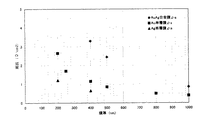
得られた各種組成割合の合金材料を、50×20×1mm程度の大きさの試験片とし、60℃、90mmHg、H2S雰囲気中に10日間放置し、その後、試験片の組成に対する硫化量と接触抵抗との関係を測定した。硫化試験前後における接触抵抗を四端子法にて測定した。また、硫化増量は、硫化試験前後における重量を、精密天秤を用いて測定した。
その結果を図1に示す。
【0016】
図1によれば、Agの重量比が増加するにつれ、硫化量が増加し、Au材料に比較して表面の経時変化が大きいことがわかる。また、Agの重量比が増加するにつれ、初期値(硫化試験を行う前のAuAg合金の接触抵抗値)に比較して、接触抵抗値の増加が大きく、半導体チップにおける電極としての信頼性を損なう可能性が認められた。
一方、Ag材料の重量比が小さい場合、下地Siへの這い上がり抑制の効果が小さくなることがわかった。
【0017】
実施例2:合金材料の作製
純度4NのAuのインゴット7.5kgと、純度4NのAgのインゴット2.5kgとをルツボに入れ、高周波溶解で溶解した後、鋳型に入れ、Au:Agが75wt%:25wt%のインゴットを作製した。
このようにして得られたAuAg合金材料は、Auの加工性と、Agの展延性をもちあわせている。
得られたインゴットを圧延して、厚さ8mmの板材とした。この板材を旋盤にて直径250mmの円盤とし、Cu製バッキングプレートに接合して、AuAg合金のターゲットを作製した。
なお、比較のために、AuAg合金のターゲットと同様に、Auターゲット、Agターゲットを同様に作製した。
【0018】
実施例3:合金材料の作製
Agの組成比を3wt%、10wt%及び40wt%とする以外は実施例2と同様の方法によりAuAg合金のターゲットを作製した。
【0019】
実施例4:合金膜の成膜
実施例2で得られたターゲットを用い、シリコン基板上に単一金属膜層としてのAuAg合金膜、Au膜及びAg膜を、それぞれスパッタリング装置を利用して、膜厚100nm〜1000nm程度に成膜した。
スパッタリング装置は、ホリゾンタル型(フェイスアップ方式)の装置であり、スパッタ面の表面クリーニングを行う逆スパッタ室と、AuAg合金ターゲット、Auターゲット又はAgターゲットを装着したスパッタ室とが、各々独立した反応室として構成されている。ターゲット電極は2重磁極型電磁石カソードを備えている。
【0020】
スパッタ条件は、反応室圧力を2mTorr〜9mTorrの範囲内で、DCパワーを0.3kW〜1kWの範囲に設定した。
このようにして形成されたAuAg合金膜は、蛍光X線による組成分析において、Agが27.5wt%、Auが72.5wt%であり、均質な膜であった。合金材料の組成よりもAgの組成比が若干増加するのは、Auに比べ質量数の小さいAgはスパッタ散乱をより受け易く、Agのスパッタ速度が速いためであると考えられる。
【0021】
また、AuAg合金膜は、Au及びAgの単一膜に比較して、スパッタリング時の圧力やDCパワーの依存性を受けにくく、成膜後の組成に大きな変化が認められず、均質な膜が形成された。
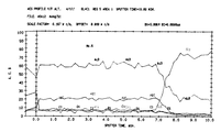
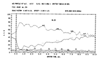
スパッタ後の合金膜及び金属膜の膜応力、窒素雰囲気下で加熱処理(380℃で40分間)した後の合金膜及び金属膜の膜応力、抵抗値をそれぞれ測定した。
得られた結果を図2〜図4に示す。なお、ここでの膜応力は、金属膜形成前後又は加熱処理後における半導体基板の反り(Bow)とうねり(Warp)で規定したものである。また、抵抗値の測定は、四探針法により室温で測定した。
【0022】
図2及び図3によれば、AuAg合金膜は、Au膜に比較して、同一膜厚では、若干ウエハ反り量及びうねり量とも増加する傾向にあるが、大きな差は認められず、十分実用に耐えうるレベルにあることが示されている。
また、図4によれば、AuAg合金膜は、Au膜に比較して、同一膜厚では、若干抵抗値が増加する傾向にあるが、大きな差は認められず、十分実用に耐えうるレベルにあることが示されている。
これにより、AuAg合金膜としての膜応力、抵抗値とも半導体チップに適用できるレベルにあることがわかった。
【0023】
実施例5:合金膜の成膜
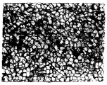
実施例4と同様に、実施例2で得られた合金材料を用いて、スパッタリング法にてシリコン基板上に200nmに成膜したAuAg合金膜と、200nmに成膜したAu膜とに対して、それぞれ窒素雰囲気下、300℃、380℃、420℃及び470℃で40分間加熱処理し、それらの膜の際表面側からオージェ分析を行うとともに、最表面の状態を電子顕微鏡にて観察した。
その結果を図5〜図9及び図10〜図14にそれぞれ示す。
【0024】
図5〜図8及び図10〜図13によれば、最表面から一定の深さまではSi、Oの濃度が低いレベルで一定していることから、AuAg合金膜は、下地シリコンの這い上がりの殆どなく、つまり、AuAg合金とシリコンとの合金化反応が、AuAgとシリコンとの界面のわずか50nmに満たない領域で起こるのみであり、また、膜表面における酸素の量が少なく、均質で表面状態があまり変化しないことが示されている。したがって、Au単体での膜に比較して、より薄い膜として使用することができる。
一方、図9及び図14によれば、Au膜では、加熱処理をすることにより、シリコンがAu膜の表面まで這い上がっており、シリコンとAuとの合金化反応(共晶)が促進されており、さらに、Au膜の表面における酸素の量がAuAg合金膜に比較して多く検出されていることが示されている。
【0025】
実施例6:合金膜の成膜
実施例3で得られたターゲットをそれぞれ用い、実施例4と同様にスパッタリング装置を利用して、シリコン基板上に、Ag組成の異なる3種のAuAg合金膜を、膜厚200nmで成膜した。
得られた各AuAg合金膜の組成を蛍光X線で分析した。その結果を表1に示す。
【0026】
【表1】

得られた各合金膜を、窒素雰囲気下、450℃の温度で40分間熱処理し、その最表面側からオージェ分析を実施した。
その結果を図15〜図17に示す。
図15〜図17によれば、いずれの組成比においても、シリコンの這い上がりを抑制することを示しており、AuAgの合金膜の最表面に酸素も検出されていないことが示されている。
【0028】
実施例7:半導体チップ
実施例4と同様の方法により、実施例2で得られターゲットを用いて、シリコンからなる半導体チップ上に、AuAg合金膜(200nm)の電極を形成し、窒素雰囲気下にて380℃で40分間、加熱処理を施した。その後の半導体チップに対するAuAg合金膜による電極の接着面強度を測定した。
その結果を表2に示す。なお、強度測定は、半導体チップの側面から加重をかけ、テンションゲージを使用して測定を行った。チップは0.6mm×0.6mmの大きさに切断し、Agペーストを用いてダイボンド加工したもので評価した。
【0029】
【表2】
表2によれば、AuAg合金膜による電極は、Au膜による電極と同等以上の接着強度を示しており、ダイボンド面での強度がチップ自体の強度よりも強いことが、破壊試験により確認できた。
【0031】
実施例8:半導体チップ
光半導体チップとしてフォトダイオードを作製した。フォトダイオードは、半導体基板上(表面)にパターニングを施し、アノード層を形成した後、実施例2で得られたAuAg合金ターゲットを用い、実施例4に示す製造方法により、半導体基板の裏側にAuAg合金膜を200nm形成し、窒素雰囲気中、380℃にて、40分間熱処理を施し、カソード電極を形成することにより、作製した。
このようなフォトダイオードに対して、逆電圧を35V印加し、100℃に加熱しながらAuAg合金材料により形成された電極のリーク電流に関する電気的特性・信頼性を評価した。その結果を図18に示す。また、フォトダイオードの短絡電流(Isc)を測定した。
その結果、リーク電流、短絡電流のいずれにおいても、Au膜に比較して、大きな特性のシフトや変動が認められず、実用的には問題がないことを確認した。
また、AuAg合金膜を用いた場合においても、Au膜を用いた場合と同様の良品歩留まりが得られた。
【0032】
実施例9:半導体チップ
光半導体チップとしてフォトトランジスタを作製した。フォトトランジスタは、半導体基板上(表面)にパターニングを施し、ベース・エミッタ層を形成した後、実施例2で得られたAuAg合金ターゲットを用い、実施例4に示す製造方法により、半導体基板の裏側にAuAg合金膜を200nm形成し、窒素雰囲気中、380℃にて40分分間熱処理を施し、コレクタ電極を形成することにより、作製した。
このフォトトランジスタを用いて、コレクタ・エミッタ間飽和電圧VCE(sat)、コレクタ・エミッタ間降伏電圧(BVCEO)を測定した。
その結果、コレクタ・エミッタ間飽和電圧VCE(sat)、コレクタ・エミッタ間降伏電圧のいずれにおいても、Au膜に比較して、特性のシフトや変動が認められず、実用的には問題がないことを確認した。
【0033】
さらに、電極としての信頼性を確認するための通電試験及び温度サイクル試験を実施したが、いずれの場合においても良好な結果が得られた。
ここで、通電試験は、常温(25℃)と高温(85℃)とで行った。測定条件として、順方向に流す電流(IF)をそれぞれ50mA(25℃時)、30mA(85℃時)とし、コレクタ・エミッタ間電力値(Pc)をそれぞれ150mW(25℃時)、70mW(85℃時)に設定した。温度サイクル試験は、−55℃と120℃とで各30分間待機を繰り返すことにより、行った。
【0034】
実施例10:半導体チップ
半導体チップとして、フォトトライアックを作製した。このフォトトライアックは、半導体基板上(表面)にパターニングを施し、ベース・エミッタ層を形成した後、実施例2で得られたAuAg合金ターゲットを用い、実施例4に示す製造方法により、半導体基板の裏側にAuAg合金膜を200nm形成し、窒素雰囲気中、380℃にて、40分間熱処理を施し、コレクタ電極を形成することにより、作製した。
このようなフォトトライアックを用いて、保持電流(IH)、オン電圧(VT)、最小トリガ電流(IFT)、繰り返しピークオフ電圧(VDRM)を測定した。
その結果、保持電流、オン電圧、最小トリガ電流、繰り返しピークオフ電圧のいずれにおいても、Au膜に比較して、特性のシフトや変動が認められず、実用的には問題がないことを確認した。
【0035】
【発明の効果】
本発明によれば、Auを主成分とし、Agを3wt%以上40wt%以下の範囲で含有してなる合金材料を用いることにより、組成が安定し、Ag単体の金属材料に比較して抵抗等の性能を安定させることが可能になる。また、加熱処理を施した前後での組成変化を最小限に抑えることができる。
特に、Au及びAgが3N以上の純度である場合には、不純物による電気的な特性の劣化を防止することができ、より高品質の金属材料を提供することが可能となる。
また、本発明の半導体用合金材料を、スパッタリングターゲット材料、蒸着用材料及びボンディング用ワイヤー材料の形態で用いることにより、従来から汎用されている方法をそのまま、特別な設備を要することなく、用いることができる。
【0036】
しかも、AuAg合金は貴金属であるため、他の金属材料に比べて回収、リサイクルが容易であり、環境に対しても配慮することが可能である。
さらに、本発明の半導体用合金材料を金属膜として形成して半導体チップ等を構成する場合には、電子機器、電子部品等の光学的及び電気的な特性を向上させることができ、より信頼性の高い電子機器、電子部品等を実現することが可能となる。しかも、加工性に優れ、機器又は部品等の歩留まりを向上させることができるとともに、AgはAuよりも安価であるために、Au単体を用いる場合に比較して、より安価な電子機器、電子部品等を提供することができる。
【図面の簡単な説明】
【図1】AuAg合金材料についてのAgの組成比に対する硫化量及び接触抵抗の関係を示すグラフである。
【図2】本発明の半導体用合金材料をシリコン基板上に形成した場合のAuAg合金膜の応力(ウエハソリ量で規定)を示す図である。
【図3】本発明の半導体用合金材料をシリコン基板上に形成した場合のAuAg合金膜の応力(ウエハうねり量で規定)を示す図である。
【図4】本発明の半導体用合金材料をシリコン基板上に形成した場合のAuAg合金膜の膜厚に対する抵抗値を示す図である。
【図5】本発明の半導体用合金材料によるAuAg合金膜(Ag25wt%)をシリコン基板上に200nm堆積し、300℃40分の加熱処理を施した後のオージェ分析によるデプスプロファイルを示す図である。
【図6】本発明の半導体用合金材料によるAuAg合金膜(Ag25wt%)をシリコン基板上に200nm堆積し、380℃40分の加熱処理を施した後のオージェ分析によるデプスプロファイルを示す図である。
【図7】本発明の半導体用合金材料によるAuAg合金膜(Ag25wt%)をシリコン基板上に200nm堆積し、420℃40分の加熱処理を施した後のオージェ分析によるデプスプロファイルを示す図である。
【図8】本発明の半導体用合金材料によるAuAg合金膜(Ag25wt%)をシリコン基板上に200nm堆積し、470℃40分の加熱処理を施した後のオージェ分析によるデプスプロファイルを示す図である。
【図9】Au膜をシリコン基板上に200nm堆積し、380℃40分の加熱処理を施した後のオージェ分析によるデプスプロファイルを示す図である。
【図10】本発明の半導体用合金材料によるAuAg合金膜(Ag25wt%)をシリコン基板上に200nm堆積し、300℃40分の加熱処理を施した後の最表面を観察したSEM写真である。
【図11】本発明の半導体用合金材料によるAuAg合金膜(Ag25wt%)をシリコン基板上に200nm堆積し、380℃40分の加熱処理を施した後の最表面を観察したSEM写真である。
【図12】本発明の半導体用合金材料によるAuAg合金膜(Ag25wt%)をシリコン基板上に200nm堆積し、420℃40分の加熱処理を施した後の最表面を観察したSEM写真である。
【図13】本発明の半導体用合金材料によるAuAg合金膜(Ag25wt%)をシリコン基板上に200nm堆積し、470℃40分の加熱処理を施した後の最表面を観察したSEM写真である。
【図14】Au膜をシリコン基板上に200nm堆積し、380℃40分の加熱処理を実施した後の最表面を観察したSEM写真である。
【図15】本発明の半導体用合金材料によるAuAg合金膜(Ag3wt%)をシリコン基板上に200nm堆積し、470℃40分の加熱処理を施した後のオージェ分析によるデプスプロファイルを示す図である。
【図16】本発明の半導体用合金材料によるAuAg合金膜(Ag10wt%)をシリコン基板上に200nm堆積し、470℃40分の加熱処理を施した後のオージェ分析によるデプスプロファイルを示す図である。
【図17】本発明の半導体用合金材料によるAuAg合金膜(Ag40wt%)をシリコン基板上に200nm堆積し、470℃40分の加熱処理を施した後のオージェ分析によるデプスプロファイルを示す図である。
【図18】本発明の半導体用合金材料によるAuAg合金膜をフォトダイオードの電極として形成した場合の電気特性(漏れ電流)を示した図である。[0001]
TECHNICAL FIELD OF THE INVENTION
The present invention relates to a semiconductor alloy material, a semiconductor chip using the alloy material, and a method for manufacturing the same, and more particularly, to an AuAg alloy material, a semiconductor chip having stabilized performance using the alloy material, and a method for manufacturing the same. .
[0002]
2. Description of the Related Art
Conventionally, Au and Ag have been used in a single layer, respectively, as a metal material for manufacturing a semiconductor device according to the purpose of use.
In general, Au is a metal material that is stable in the atmosphere and highly extensible, does not react with other materials or components in the atmosphere even when heated, and can maintain a clean metal surface. Since Ag is inexpensive and has low resistance, it is widely used as a metal material for semiconductors.
However, when the Au film is directly coated on the Si layer, the subsequent heat treatment diffuses Si into the Au, so that the composition of the Au film is not stable and may deteriorate the physical properties of the film.
When Ag is used as a single metal film, it is easily sulfided and recrystallized and softened by self-annealing.
[0003]
For this reason, for example, as an Au and Ag-containing alloy material, Ag is a main component, Au is contained in an amount of 0.1 wt% to 10 wt%, and at least one of elements such as Cu, Al, and Ti is 0%. It has been proposed that an alloy material containing not less than 1 wt% and not more than 5 wt% is used for electronic components, electronic devices, electronic optical components, and the like (for example, Patent Document 1). Such an alloy material, that is, an alloy material in which Au, Ag, and the like contain Cu, Al, Ti, and the like, is used to improve the stability and workability of the material and reduce the resistivity of the wiring. ing.
Also, for example, a method of forming an alloy layer of Au and Ag by sputtering using a single metal Au and Ag processed in a mosaic shape as a target material used in sputtering, There is a method of forming a multilayer film of an Au film and an Ag film using Au and Ag of one metal as separate target materials, and then diffusing both to form an alloy layer of Au and Ag. .
[0004]
However, when an alloy layer is formed using these targets, there is a problem that the obtained alloy layer is not uniform, and the composition stability of the alloy layer is deteriorated. Furthermore, in the method by diffusion after the formation of the multilayer film, not only the number of steps is increased and the process becomes complicated, but also homogenization by diffusion is limited, and it is also difficult to uniformly form the alloy layer.
That is, in order to compensate for the disadvantages of Au and Ag and maximize the advantages of both, at present, a single film of an alloy of Au and Ag is not used for semiconductor applications.
[0005]
The present invention has been made in view of the above problems, and by using a single film made of an alloy of Au and Ag, maximizes the unique physical properties of each single metal film to obtain a uniform and stable film. An object of the present invention is to provide an alloy material having a composition and excellent workability, and to provide a semiconductor chip using such an alloy material and a method for manufacturing the same.
[0006]
[Means for Solving the Problems]
According to the present invention, there is provided an alloy material for semiconductors containing Au as a main component and containing Ag in a range of 3 wt% or more and 40 wt% or less.
Further, according to the present invention, there is provided a semiconductor chip in which a metal film made of the above alloy material is formed on a semiconductor substrate.
Further, according to the present invention, there is provided a method of manufacturing a semiconductor chip, wherein a metal film is formed on a semiconductor substrate using the above alloy material.
[0007]
BEST MODE FOR CARRYING OUT THE INVENTION
The alloy material for a semiconductor of the present invention contains Au as a main component and contains Ag in a range of 3 wt% or more and 40 wt% or less. Here, “for semiconductor” means an alloy material used for forming a semiconductor device such as a semiconductor device or a semiconductor chip, or an alloy material used in a manufacturing process of the semiconductor device. Further, the alloy material is a material in which Au and Ag are uniformly dissolved, or a material having a uniform crystal phase of Au and Ag, in which Au and Ag randomly occupy lattice points. Either a solid solution or a eutectic alloy may be used, but a solid solution, particularly a complete solid solution is suitable.
[0008]
Ag constituting the alloy material for semiconductor is preferably 5 wt% or more, 10 wt% or more, 15 wt% or more, and 20 wt% or more. Further, those having 35 wt% or less, 30 wt% or less, and 25 wt% or less are preferable. Among them, those having a content of 10 wt% or more and 30 wt% or less are more preferable. However, when the ratio of Ag is small and the AuAg alloy is formed directly on the silicon substrate as a thin film, the effect of suppressing the diffusion of silicon is reduced. Therefore, Ag is more preferably 10 wt% or more. Further, in order to suppress a shift in electrical characteristics due to an increase in contact resistance, the content is more preferably 30 wt% or less.
Au and Ag are, for example, 3N each when applied to a semiconductor chip in order to ensure the reliability and the like of the semiconductor chip without impairing electrical characteristics such as leak current when applied to a semiconductor chip. (99.9%) or higher, preferably 4N or higher, more preferably 5N or higher.
[0009]
The alloy material for semiconductor of the present invention is a method known in the art, for example, a method of melting an ingot of Au and Ag by high frequency melting to form an alloy, mixing Au powder and Ag powder, and sintering. It can be manufactured by a method of forming an alloy.
As a result, various problems caused by Au alone, for example, the diffusion of the underlying Si when directly formed on the Si layer can be significantly reduced, and a stable coating composition without Si diffusion can be maintained. To improve weather resistance and metal strength.
[0010]
The alloy material for a semiconductor of the present invention can be used for various applications. For example, a semiconductor device or semiconductor chip including an electronic device, an electronic component, an electro-optical component, specifically, a wiring, an electrode, a bump, a light-shielding film, a contact or a wire via a metal paste (an optical transmission unit, a remote control light-receiving unit) Unit, PC / GP unit, DRAM, flash memory, CPU, MPU, ASIC, LSI, TFT, semiconductor laser, solar cell, light emitting element, CCD, thyristor, photodiode, phototransistor, power transistor, etc.), liquid crystal display panel (A flat panel display, a reflection type and a transmission type liquid crystal display panel, and the like). Typically, it can be used in the form of a sputtering target material, a deposition material, or a bonding wire material.
[0011]
In particular, when used for the above-described equipment and components, the thickness of the metal material is not particularly limited, but for example, it is used in a thickness of 50 nm or more and 1000 nm or less in consideration of the stress of the alloy film. Is preferred. That is, if the stress becomes large, there may be a manufacturing defect such as a probe (measurement needle) not being able to properly contact at the time of a wafer test or the like. However, when a wafer test or the like is not necessary, or when it is used for a bump or a plating process to be performed thereafter, the thickness of the alloy film can be freely set.
[0012]
The alloy material for a semiconductor of the present invention can be used as a metal film formed on a semiconductor substrate by various methods. For example, it can flexibly and widely correspond to existing semiconductor processes such as a sputtering method, a vapor deposition method, a plating method, and a bonding method.
Specifically, in the vapor deposition method, for example, an AuAg alloy wire having a wire diameter of 1 mmφ is installed in a crucible, and 3 × 10⁻⁶By heating while maintaining a degree of vacuum of about Torr, an AuAg alloy film having a uniform composition can be formed. In the plating method, for example, AuAg alloy plating solution of alkali cyanide is used, and 0.5 A / dm.2An AuAg alloy film can be deposited by plating at a current density of the order. In the bonding wire method, an ingot of an AuAg alloy is produced by a melt casting method, and is extruded and repeatedly drawn to finally form a fine wire having a wire diameter of about 20 to 30 μm. And an alloy wire for a bonding wire for connection to an external electrode on a lead frame can be formed and used. In the case where the AuAg alloy material is patterned and used as a wiring, an electrode, a bump material, or the like, in addition to the processing by the lift-off method, depending on the composition ratio of the AuAg alloy material, an aqueous solution of potassium iodide or an aqueous solution of potassium iodide is used. Etching can be easily performed by using a mixed solution of phosphoric acid-based etching and the like. By processing the AuAg alloy at an appropriate position in an appropriate size, etc., two or more types of wiring, electrodes, bumps, light shielding films, contacts, etc., for example, wiring and electrodes, light shielding films and electrodes, bumps and electrodes, Wiring, contacts, and the like can be formed in the same step.
Incidentally, the alloy material for semiconductor of the present invention, when used by any method such as sputtering method, vapor deposition method, the obtained alloy material shows almost the same resistance value, stress, elongation, strength, etc. It is possible to easily and reliably form a film.
[0013]
In the present invention, a metal film made of an AuAg alloy material is formed on a semiconductor chip, a semiconductor substrate, a semiconductor layer (for example, an element semiconductor such as silicon or germanium, or a compound semiconductor such as GaAs) at 300 ° C. The heat treatment is preferably performed in a temperature range of at least 520 ° C. Thereby, a stable contact with a semiconductor layer (for example, silicon or the like) can be secured. For example, when Al or AlSi alloy, which is a representative metal, is used as a front electrode of a semiconductor substrate and an AuAg alloy is used as a back electrode, an Al spike (a phenomenon in which Al enters a semiconductor substrate) or an increase in resistance at a contact is caused. Etc. can be prevented.
[0014]
Above all, when an AuAg alloy is formed on a silicon layer, heat treatment is performed in a temperature range of 300 ° C. to 470 ° C. so as to suppress the eutectic of Au—Ag—Si and not deteriorate the characteristics of a semiconductor chip or the like. Is preferred. In such a temperature range, it is possible to suppress the base Si from creeping up to the AuAg alloy, the alloying reaction between the base Si and AuAg, the generation of oxides on the outermost surface of the AuAg alloy, and the like. In this case, the uniform composition of the AuAg alloy film does not change, the composition becomes stable against heat, and the AuAg alloy film can be used as a thinner film. Furthermore, this makes it possible to improve the bonding strength of the connection surface at the time of chip die bonding or wire bonding, becomes compatible with the metal paste, and provide various highly reliable components and devices. Become.
Hereinafter, the alloy material, the semiconductor chip, and the method of manufacturing the same according to the present invention will be described in detail.
[0015]
Example 1: Preparation of alloy material
An Au ingot and an Ag ingot were weighed so that Au and Ag had various ratios, melted by high frequency melting, and then poured into a mold to produce an AuAg alloy material. Note that 4N material was used for both Au and Ag.
The obtained alloy materials having various composition ratios were used as test pieces having a size of about 50 × 20 × 1 mm, and 60 ° C., 90 mmHg, H2It was left in an S atmosphere for 10 days, and then the relationship between the sulfur content and the contact resistance with respect to the composition of the test piece was measured. The contact resistance before and after the sulfuration test was measured by a four-terminal method. The weight increase before and after the sulfurization test was measured using a precision balance.
The result is shown in FIG.
[0016]
FIG. 1 shows that as the weight ratio of Ag increases, the amount of sulfuration increases, and the surface changes over time are larger than those of the Au material. Further, as the weight ratio of Ag increases, the contact resistance increases more than the initial value (the contact resistance of the AuAg alloy before the sulfuration test is performed), which impairs the reliability as an electrode in the semiconductor chip. The possibility was recognized.
On the other hand, it was found that when the weight ratio of the Ag material was small, the effect of suppressing creeping up to the underlying Si was reduced.
[0017]
Example 2: Preparation of alloy material
7.5 kg of a 4N-purity Au ingot and 2.5 kg of a 4N-purity Ag ingot are placed in a crucible, melted by high frequency melting, and then placed in a mold to produce an ingot of Au: Ag of 75 wt%: 25 wt%. did.
The AuAg alloy material thus obtained has the workability of Au and the spreadability of Ag.
The obtained ingot was rolled to obtain a plate material having a thickness of 8 mm. This plate was turned into a disk having a diameter of 250 mm using a lathe and joined to a Cu backing plate to produce a target of an AuAg alloy.
For comparison, an Au target and an Ag target were produced in the same manner as the AuAg alloy target.
[0018]
Example 3: Preparation of alloy material
An AuAg alloy target was produced in the same manner as in Example 2 except that the composition ratio of Ag was 3 wt%, 10 wt%, and 40 wt%.
[0019]
Example 4: Formation of alloy film
Using the target obtained in Example 2, an AuAg alloy film, an Au film, and an Ag film as a single metal film layer were formed on a silicon substrate to a thickness of about 100 nm to 1000 nm using a sputtering apparatus. did.
The sputtering apparatus is a horizontal type (face-up type) apparatus, in which a reverse sputtering chamber for cleaning the surface of the sputtering surface and a sputtering chamber equipped with an AuAg alloy target, an Au target or an Ag target are independent reaction chambers. It is configured as The target electrode has a double pole type electromagnet cathode.
[0020]
The sputtering conditions were such that the reaction chamber pressure was in the range of 2 mTorr to 9 mTorr and the DC power was in the range of 0.3 kW to 1 kW.
The AuAg alloy film thus formed was a homogeneous film having 27.5% by weight of Ag and 72.5% by weight of Au in the composition analysis by X-ray fluorescence. It is considered that the reason why the composition ratio of Ag is slightly larger than the composition of the alloy material is that Ag having a smaller mass number is more susceptible to spatter scattering than Au and has a higher Ag sputter rate.
[0021]
In addition, compared to a single film of Au and Ag, the AuAg alloy film is less susceptible to dependency on the pressure and DC power at the time of sputtering, does not show a large change in the composition after film formation, and a uniform film is obtained. Been formed.
The film stress of the alloy film and the metal film after the sputtering, the film stress of the alloy film and the metal film after the heat treatment (380 ° C. for 40 minutes) in a nitrogen atmosphere, and the resistance value were measured.
The obtained results are shown in FIGS. Here, the film stress is defined by the warpage (Bow) and the swell (Warp) of the semiconductor substrate before and after the formation of the metal film or after the heat treatment. The resistance was measured at room temperature by a four-probe method.
[0022]
According to FIGS. 2 and 3, the AuAg alloy film has a tendency to slightly increase both the wafer warpage amount and the waviness amount at the same film thickness as compared with the Au film, but there is no large difference, and the AuAg alloy film is sufficiently practical. It is shown to be at a level that can withstand.
According to FIG. 4, the AuAg alloy film has a tendency to have a slightly increased resistance value at the same film thickness as compared with the Au film, but no large difference is recognized, and the AuAg alloy film has a sufficient level for practical use. It is shown that there is.
Thus, it was found that both the film stress and the resistance value of the AuAg alloy film were at a level applicable to a semiconductor chip.
[0023]
Example 5: Formation of alloy film
In the same manner as in Example 4, using the alloy material obtained in Example 2, an AuAg alloy film formed on a silicon substrate to a thickness of 200 nm and an Au film formed to a thickness of 200 nm on a silicon substrate by a sputtering method. Heat treatment was performed at 300 ° C., 380 ° C., 420 ° C., and 470 ° C. for 40 minutes in a nitrogen atmosphere, Auger analysis was performed from the surface side of these films, and the state of the outermost surface was observed with an electron microscope.
The results are shown in FIGS. 5 to 9 and FIGS. 10 to 14, respectively.
[0024]
According to FIG. 5 to FIG. 8 and FIG. 10 to FIG. 13, since the concentration of Si and O is constant at a low level at a certain depth from the outermost surface, the AuAg alloy film is Almost no, that is, the alloying reaction between the AuAg alloy and silicon occurs only in a region of less than 50 nm at the interface between the AuAg and silicon. Does not change much. Therefore, it can be used as a thinner film as compared with a film of Au alone.
On the other hand, according to FIG. 9 and FIG. 14, in the Au film, the silicon is crawled up to the surface of the Au film by the heat treatment, and the alloying reaction (eutectic) between silicon and Au is promoted. Further, it is shown that the amount of oxygen on the surface of the Au film is detected more than that of the AuAg alloy film.
[0025]
Example 6: Formation of alloy film
Three types of AuAg alloy films having different Ag compositions were formed to a thickness of 200 nm on a silicon substrate by using the targets obtained in Example 3 and using a sputtering apparatus in the same manner as in Example 4.
The composition of each of the obtained AuAg alloy films was analyzed by X-ray fluorescence. Table 1 shows the results.
[0026]
[Table 1]
Each of the obtained alloy films was heat-treated under a nitrogen atmosphere at a temperature of 450 ° C. for 40 minutes, and Auger analysis was performed from the outermost surface side.
The results are shown in FIGS.
FIGS. 15 to 17 show that the silicon crawling is suppressed at any composition ratio, and that no oxygen is detected on the outermost surface of the AuAg alloy film.
[0028]
Example 7: Semiconductor chip
An electrode of an AuAg alloy film (200 nm) was formed on a semiconductor chip made of silicon by using the target obtained in Example 2 in the same manner as in Example 4, and the electrode was formed at 380 ° C. for 40 minutes in a nitrogen atmosphere. And a heat treatment. Thereafter, the bonding surface strength of the electrode with the AuAg alloy film to the semiconductor chip was measured.
Table 2 shows the results. The strength was measured by applying a weight from the side surface of the semiconductor chip and using a tension gauge. The chip was cut into a size of 0.6 mm × 0.6 mm and die-bonded using an Ag paste for evaluation.
[0029]
[Table 2]
According to Table 2, the electrode made of the AuAg alloy film showed an adhesive strength equal to or higher than that of the electrode made of the Au film, and it was confirmed by a destructive test that the strength on the die bond surface was stronger than the strength of the chip itself. .
[0031]
Example 8: Semiconductor chip
A photodiode was manufactured as an optical semiconductor chip. The photodiode is patterned on the semiconductor substrate (front surface) to form an anode layer, and then the AuAg alloy target obtained in Example 2 is used to produce AuAg on the back side of the semiconductor substrate by the manufacturing method described in Example 4. An alloy film was formed to a thickness of 200 nm and heat-treated in a nitrogen atmosphere at 380 ° C. for 40 minutes to form a cathode electrode.
A reverse voltage of 35 V was applied to such a photodiode, and while heating to 100 ° C., electrical characteristics and reliability of an electrode formed of an AuAg alloy material with respect to a leak current were evaluated. FIG. 18 shows the result. Further, the short-circuit current (Isc) of the photodiode was measured.
As a result, no significant shift or fluctuation of characteristics was observed in any of the leak current and the short-circuit current as compared with the Au film, and it was confirmed that there was no problem in practice.
In addition, even when the AuAg alloy film was used, the same good product yield as that when the Au film was used was obtained.
[0032]
Embodiment 9: Semiconductor chip
A phototransistor was manufactured as an optical semiconductor chip. The phototransistor is formed on the semiconductor substrate (surface) by patterning to form a base / emitter layer, and then using the AuAg alloy target obtained in Example 2 by the manufacturing method described in Example 4 to form the backside of the semiconductor substrate. An AuAg alloy film was formed to a thickness of 200 nm and heat-treated at 380 ° C. for 40 minutes in a nitrogen atmosphere to form a collector electrode.
Using this phototransistor, the collector-emitter saturation voltage VCE (sat) and the collector-emitter breakdown voltage (BVCEO) were measured.
As a result, neither the shift nor the fluctuation of the characteristics are recognized in comparison with the Au film in any of the collector-emitter saturation voltage VCE (sat) and the collector-emitter breakdown voltage, and there is no practical problem. It was confirmed.
[0033]
Further, an energization test and a temperature cycle test were performed to confirm the reliability of the electrode, and good results were obtained in each case.
Here, the energization test was performed at normal temperature (25 ° C.) and high temperature (85 ° C.). As the measurement conditions, the forward current (IF) was 50 mA (at 25 ° C.) and 30 mA (at 85 ° C.), respectively, and the collector-emitter power value (Pc) was 150 mW (at 25 ° C.) and 70 mW (85 ° C., respectively). ° C). The temperature cycle test was performed by repeating standby for 30 minutes at -55 ° C and 120 ° C.
[0034]
Example 10: Semiconductor chip
A phototriac was manufactured as a semiconductor chip. This phototriac is obtained by patterning a semiconductor substrate (surface) to form a base / emitter layer and then using the AuAg alloy target obtained in Example 2 by the manufacturing method shown in Example 4 to form a semiconductor substrate. A 200 nm AuAg alloy film was formed on the back side, and heat treatment was performed at 380 ° C. for 40 minutes in a nitrogen atmosphere to form a collector electrode.
Using such a phototriac, a holding current (IH), an ON voltage (VT), a minimum trigger current (IFT), and a repetitive peak OFF voltage (VDRM) were measured.
As a result, in any of the holding current, the on-voltage, the minimum trigger current, and the repetitive peak-off voltage, no shift or change in the characteristics was observed as compared with the Au film, and it was confirmed that there was no practical problem.
[0035]
【The invention's effect】
According to the present invention, by using an alloy material containing Au as a main component and containing Ag in a range of 3 wt% or more and 40 wt% or less, the composition is stable, and the resistance and the like are higher than the metal material of Ag alone. Performance can be stabilized. In addition, a change in composition before and after the heat treatment can be minimized.
In particular, when Au and Ag have a purity of 3N or more, deterioration of electrical characteristics due to impurities can be prevented, and a higher quality metal material can be provided.
In addition, by using the alloy material for a semiconductor of the present invention in the form of a sputtering target material, a vapor deposition material, and a bonding wire material, it is possible to use a conventionally widely used method without any special equipment. Can be.
[0036]
Moreover, since the AuAg alloy is a noble metal, it can be easily collected and recycled compared to other metal materials, and it is possible to consider the environment.
Furthermore, when a semiconductor chip or the like is formed by forming the alloy material for a semiconductor of the present invention as a metal film, the optical and electrical characteristics of electronic devices, electronic components, and the like can be improved, and the reliability can be improved. It is possible to realize electronic devices, electronic components, and the like with high reliability. In addition, since the processability is excellent, the yield of devices or parts can be improved, and Ag is cheaper than Au, electronic devices and electronic components that are more inexpensive than when Au alone is used. Etc. can be provided.
[Brief description of the drawings]
FIG. 1 is a graph showing a relationship between a sulfur content and a contact resistance with respect to a composition ratio of Ag in an AuAg alloy material.
FIG. 2 is a diagram showing the stress (defined by the amount of wafer warpage) of an AuAg alloy film when a semiconductor alloy material of the present invention is formed on a silicon substrate.
FIG. 3 is a view showing the stress (defined by the amount of undulation of a wafer) of an AuAg alloy film when the semiconductor alloy material of the present invention is formed on a silicon substrate.
FIG. 4 is a diagram showing a resistance value with respect to a film thickness of an AuAg alloy film when a semiconductor alloy material of the present invention is formed on a silicon substrate.
FIG. 5 is a diagram showing a depth profile by Auger analysis after depositing a 200 nm AuAg alloy film (Ag 25 wt%) using a semiconductor alloy material of the present invention on a silicon substrate and performing a heat treatment at 300 ° C. for 40 minutes. .
FIG. 6 is a diagram showing a depth profile by Auger analysis after depositing a 200 nm AuAg alloy film (Ag 25 wt%) using a semiconductor alloy material of the present invention on a silicon substrate and performing heat treatment at 380 ° C. for 40 minutes. .
FIG. 7 is a diagram showing a depth profile by Auger analysis after depositing a 200 nm AuAg alloy film (Ag 25 wt%) using a semiconductor alloy material of the present invention on a silicon substrate and performing a heat treatment at 420 ° C. for 40 minutes. .
FIG. 8 is a diagram showing a depth profile by Auger analysis after an AuAg alloy film (Ag 25 wt%) made of a semiconductor alloy material of the present invention is deposited to a thickness of 200 nm on a silicon substrate and subjected to a heat treatment at 470 ° C. for 40 minutes. .
FIG. 9 is a diagram showing a depth profile by Auger analysis after depositing a 200 nm Au film on a silicon substrate and performing a heat treatment at 380 ° C. for 40 minutes.
FIG. 10 is an SEM photograph in which the outermost surface is observed after a 200 nm AuAg alloy film (Ag 25 wt%) made of a semiconductor alloy material of the present invention is deposited on a silicon substrate and subjected to a heat treatment at 300 ° C. for 40 minutes.
FIG. 11 is an SEM photograph showing the outermost surface after a 200 nm AuAg alloy film (Ag 25 wt%) made of a semiconductor alloy material of the present invention is deposited on a silicon substrate and subjected to a heat treatment at 380 ° C. for 40 minutes.
FIG. 12 is an SEM photograph in which an AuAg alloy film (Ag 25 wt%) made of a semiconductor alloy material according to the present invention is deposited to a thickness of 200 nm on a silicon substrate and subjected to a heat treatment at 420 ° C. for 40 minutes.
FIG. 13 is an SEM photograph showing the outermost surface after a 200 nm AuAg alloy film (Ag 25 wt%) made of a semiconductor alloy material of the present invention is deposited on a silicon substrate and subjected to a heat treatment at 470 ° C. for 40 minutes.
FIG. 14 is an SEM photograph showing the outermost surface after depositing a 200 nm Au film on a silicon substrate and performing a heat treatment at 380 ° C. for 40 minutes.
FIG. 15 is a diagram showing a depth profile by Auger analysis after depositing a 200 nm AuAg alloy film (
FIG. 16 is a view showing a depth profile by Auger analysis after depositing a 200 nm AuAg alloy film (
FIG. 17 is a diagram showing a depth profile by Auger analysis after an AuAg alloy film (
FIG. 18 is a view showing electric characteristics (leakage current) when an AuAg alloy film made of a semiconductor alloy material of the present invention is formed as an electrode of a photodiode.
Claims (10)
Priority Applications (7)
| Application Number | Priority Date | Filing Date | Title |
|---|---|---|---|
| JP2002342797A JP2004179327A (en) | 2002-11-26 | 2002-11-26 | Alloy material for semiconductor, semiconductor chip using the same and method for manufacturing semiconductor chip |
| CNB2003801042815A CN100386848C (en) | 2002-11-26 | 2003-10-29 | Alloy material for semiconductor, semiconductor chip using such alloy material, and method for manufacturing same |
| AU2003280621A AU2003280621A1 (en) | 2002-11-26 | 2003-10-29 | Alloy material for semiconductor, semiconductor chip using such alloy material, and method for manufacturing same |
| US10/536,406 US20060226546A1 (en) | 2002-11-26 | 2003-10-29 | Alloy material for semiconductors, semiconductor chip using the alloy material and production method of the same |
| PCT/JP2003/013890 WO2004049415A1 (en) | 2002-11-26 | 2003-10-29 | Alloy material for semiconductor, semiconductor chip using such alloy material, and method for manufacturing same |
| KR1020057009567A KR100742672B1 (en) | 2002-11-26 | 2003-10-29 | Alloy material for semiconductor, semiconductor chip using such alloy material, and method for manufacturing same |
| TW092133066A TW200416748A (en) | 2002-11-26 | 2003-11-25 | Alloy material for semiconductor, semiconductor chip using such alloy material, and method for manufacturing the same |
Applications Claiming Priority (1)
| Application Number | Priority Date | Filing Date | Title |
|---|---|---|---|
| JP2002342797A JP2004179327A (en) | 2002-11-26 | 2002-11-26 | Alloy material for semiconductor, semiconductor chip using the same and method for manufacturing semiconductor chip |
Publications (2)
| Publication Number | Publication Date |
|---|---|
| JP2004179327A true JP2004179327A (en) | 2004-06-24 |
| JP2004179327A5 JP2004179327A5 (en) | 2005-09-29 |
Family
ID=32375901
Family Applications (1)
| Application Number | Title | Priority Date | Filing Date |
|---|---|---|---|
| JP2002342797A Pending JP2004179327A (en) | 2002-11-26 | 2002-11-26 | Alloy material for semiconductor, semiconductor chip using the same and method for manufacturing semiconductor chip |
Country Status (7)
| Country | Link |
|---|---|
| US (1) | US20060226546A1 (en) |
| JP (1) | JP2004179327A (en) |
| KR (1) | KR100742672B1 (en) |
| CN (1) | CN100386848C (en) |
| AU (1) | AU2003280621A1 (en) |
| TW (1) | TW200416748A (en) |
| WO (1) | WO2004049415A1 (en) |
Families Citing this family (4)
| Publication number | Priority date | Publication date | Assignee | Title |
|---|---|---|---|---|
| KR101107862B1 (en) * | 2006-12-21 | 2012-01-31 | 가부시키가이샤 고베 세이코쇼 | Alloy coating film for metal separator of fuel cell, method for producing the same, sputtering target material, metal separator and fuel cell |
| JP4176133B1 (en) * | 2007-06-06 | 2008-11-05 | 田中貴金属工業株式会社 | Probe pin |
| JP5116101B2 (en) * | 2007-06-28 | 2013-01-09 | 新日鉄住金マテリアルズ株式会社 | Bonding wire for semiconductor mounting and manufacturing method thereof |
| DE102014111895A1 (en) * | 2014-08-20 | 2016-02-25 | Infineon Technologies Ag | Metallized electrical component |
Family Cites Families (12)
| Publication number | Priority date | Publication date | Assignee | Title |
|---|---|---|---|---|
| US3770496A (en) * | 1971-06-25 | 1973-11-06 | Du Pont | Elimination of dielectric degradation in printed bold/dielectric/palladium-silver structures |
| JPS54144870A (en) * | 1978-05-04 | 1979-11-12 | Mitsubishi Electric Corp | Wire bonding method for semiconductor element |
| JPS60254761A (en) * | 1984-05-31 | 1985-12-16 | Sumitomo Electric Ind Ltd | Lead frame for semiconductor device |
| JPS6173326A (en) * | 1984-09-19 | 1986-04-15 | Hitachi Ltd | Manufacture of semiconductor device |
| JPH03155134A (en) * | 1989-11-13 | 1991-07-03 | Seiko Epson Corp | Wiring electrode of integrated circuit |
| US5364706A (en) * | 1990-07-20 | 1994-11-15 | Tanaka Denshi Kogyo Kabushiki Kaisha | Clad bonding wire for semiconductor device |
| JPH05109818A (en) * | 1991-10-16 | 1993-04-30 | Hitachi Chem Co Ltd | Semiconductor chip connection structure |
| EP0594286B1 (en) * | 1992-08-27 | 1998-11-25 | Kabushiki Kaisha Toshiba | Electronic parts with metal wiring and manufacturing method thereof |
| JPH118341A (en) * | 1997-06-18 | 1999-01-12 | Mitsui High Tec Inc | Lead frame for semiconductor device |
| JPH11233783A (en) * | 1998-02-17 | 1999-08-27 | Sharp Corp | Thin film transistor and its manufacturing method |
| WO2002023618A1 (en) * | 2000-09-18 | 2002-03-21 | Nippon Steel Corporation | Bonding wire for semiconductor and method of manufacturing the bonding wire |
| JP3707548B2 (en) * | 2002-03-12 | 2005-10-19 | 株式会社三井ハイテック | Lead frame and lead frame manufacturing method |
-
2002
- 2002-11-26 JP JP2002342797A patent/JP2004179327A/en active Pending
-
2003
- 2003-10-29 WO PCT/JP2003/013890 patent/WO2004049415A1/en active Application Filing
- 2003-10-29 US US10/536,406 patent/US20060226546A1/en not_active Abandoned
- 2003-10-29 AU AU2003280621A patent/AU2003280621A1/en not_active Abandoned
- 2003-10-29 KR KR1020057009567A patent/KR100742672B1/en active IP Right Grant
- 2003-10-29 CN CNB2003801042815A patent/CN100386848C/en not_active Expired - Lifetime
- 2003-11-25 TW TW092133066A patent/TW200416748A/en not_active IP Right Cessation
Also Published As
| Publication number | Publication date |
|---|---|
| AU2003280621A1 (en) | 2004-06-18 |
| KR100742672B1 (en) | 2007-07-25 |
| CN100386848C (en) | 2008-05-07 |
| US20060226546A1 (en) | 2006-10-12 |
| KR20050088086A (en) | 2005-09-01 |
| WO2004049415A1 (en) | 2004-06-10 |
| TW200416748A (en) | 2004-09-01 |
| AU2003280621A8 (en) | 2004-06-18 |
| TWI304220B (en) | 2008-12-11 |
| CN1717783A (en) | 2006-01-04 |
Similar Documents
| Publication | Publication Date | Title |
|---|---|---|
| JP3462720B2 (en) | N-type nitride semiconductor electrode, semiconductor element having the electrode, and method of manufacturing the same | |
| US8624397B2 (en) | Electrode layer structure for a thin-film transistor and process for manufacture thereof | |
| CN100334239C (en) | Ag-base alloy distribution electrode film, Ag-base alloy sputtering target for panel display | |
| JP2002511190A (en) | Method and apparatus for self-doping cathode and anode for silicon solar cells and other devices | |
| JPH03133176A (en) | Silicon carbide semiconductor device and manufacture thereof | |
| TW201230202A (en) | Sputtering target and method for manufacturing semiconductor device | |
| JP2010212465A (en) | THIN-FILM TRANSISTOR USING BARRIER LAYER AS STRUCTURE LAYER, AND Cu ALLOY SPUTTERING TARGET USED FOR SPUTTERING DEPOSITION OF THE BARRIER LAYER | |
| JP2003318454A (en) | Thermoelectric conversion element and thermoelectric module | |
| JP2004179327A (en) | Alloy material for semiconductor, semiconductor chip using the same and method for manufacturing semiconductor chip | |
| JP2565655B2 (en) | Low resistance compound | |
| KR20200023101A (en) | Thermoelectric module | |
| JP7283053B2 (en) | Silicon carbide semiconductor device, silicon carbide semiconductor assembly, and method for manufacturing silicon carbide semiconductor device | |
| KR20180022611A (en) | Thermoelectric element and thermoelectric module including the same | |
| WO2016157589A1 (en) | Ubm electrode structure for radiation detector, radiation detector, and method for manufacturing said detector and structure | |
| JP6434859B2 (en) | Al alloy film for power semiconductor devices | |
| JP2005277343A (en) | Thermoelectric conversion element and manufacturing method therefor | |
| US20230420257A1 (en) | Chip with a Silicon Carbide Substrate | |
| Nielsen | Compound formation and energy levels at the interface betweeb amorphous Se and Cu, Ag and Al electrodes | |
| JPS63253633A (en) | Manufacture of semiconductor device | |
| JPH02307224A (en) | Semiconductor device and manufacture thereof | |
| JP5368806B2 (en) | Al alloy film for display device and display device | |
| JP2002124486A (en) | Method of manufacturing electrode of compound semiconductor | |
| JP2003017720A (en) | Photo-electric conversion device | |
| JPH09115856A (en) | Ohmic electrode and formation thereof | |
| JPS62163324A (en) | Forming method for ohmic contact |
Legal Events
| Date | Code | Title | Description |
|---|---|---|---|
| A521 | Request for written amendment filed |
Free format text: JAPANESE INTERMEDIATE CODE: A523 Effective date: 20050427 |
|
| A621 | Written request for application examination |
Free format text: JAPANESE INTERMEDIATE CODE: A621 Effective date: 20050427 |
|
| A131 | Notification of reasons for refusal |
Free format text: JAPANESE INTERMEDIATE CODE: A131 Effective date: 20081209 |
|
| A521 | Request for written amendment filed |
Free format text: JAPANESE INTERMEDIATE CODE: A523 Effective date: 20090129 |
|
| A02 | Decision of refusal |
Free format text: JAPANESE INTERMEDIATE CODE: A02 Effective date: 20090407 |