JP2004165605A - Semiconductor unit, semiconductor module, and memory system - Google Patents
Semiconductor unit, semiconductor module, and memory system Download PDFInfo
- Publication number
- JP2004165605A JP2004165605A JP2003103681A JP2003103681A JP2004165605A JP 2004165605 A JP2004165605 A JP 2004165605A JP 2003103681 A JP2003103681 A JP 2003103681A JP 2003103681 A JP2003103681 A JP 2003103681A JP 2004165605 A JP2004165605 A JP 2004165605A
- Authority
- JP
- Japan
- Prior art keywords
- semiconductor
- wiring
- input
- signal
- module
- Prior art date
- Legal status (The legal status is an assumption and is not a legal conclusion. Google has not performed a legal analysis and makes no representation as to the accuracy of the status listed.)
- Granted
Links
Images


Classifications
-
- H—ELECTRICITY
- H01—ELECTRIC ELEMENTS
- H01L—SEMICONDUCTOR DEVICES NOT COVERED BY CLASS H10
- H01L25/00—Assemblies consisting of a plurality of individual semiconductor or other solid state devices ; Multistep manufacturing processes thereof
- H01L25/03—Assemblies consisting of a plurality of individual semiconductor or other solid state devices ; Multistep manufacturing processes thereof all the devices being of a type provided for in the same subgroup of groups H01L27/00 - H01L33/00, or in a single subclass of H10K, H10N, e.g. assemblies of rectifier diodes
- H01L25/10—Assemblies consisting of a plurality of individual semiconductor or other solid state devices ; Multistep manufacturing processes thereof all the devices being of a type provided for in the same subgroup of groups H01L27/00 - H01L33/00, or in a single subclass of H10K, H10N, e.g. assemblies of rectifier diodes the devices having separate containers
- H01L25/105—Assemblies consisting of a plurality of individual semiconductor or other solid state devices ; Multistep manufacturing processes thereof all the devices being of a type provided for in the same subgroup of groups H01L27/00 - H01L33/00, or in a single subclass of H10K, H10N, e.g. assemblies of rectifier diodes the devices having separate containers the devices being of a type provided for in group H01L27/00
-
- H—ELECTRICITY
- H01—ELECTRIC ELEMENTS
- H01L—SEMICONDUCTOR DEVICES NOT COVERED BY CLASS H10
- H01L23/00—Details of semiconductor or other solid state devices
- H01L23/552—Protection against radiation, e.g. light or electromagnetic waves
-
- H—ELECTRICITY
- H01—ELECTRIC ELEMENTS
- H01L—SEMICONDUCTOR DEVICES NOT COVERED BY CLASS H10
- H01L23/00—Details of semiconductor or other solid state devices
- H01L23/58—Structural electrical arrangements for semiconductor devices not otherwise provided for, e.g. in combination with batteries
- H01L23/60—Protection against electrostatic charges or discharges, e.g. Faraday shields
-
- H—ELECTRICITY
- H01—ELECTRIC ELEMENTS
- H01L—SEMICONDUCTOR DEVICES NOT COVERED BY CLASS H10
- H01L23/00—Details of semiconductor or other solid state devices
- H01L23/58—Structural electrical arrangements for semiconductor devices not otherwise provided for, e.g. in combination with batteries
- H01L23/64—Impedance arrangements
-
- H—ELECTRICITY
- H01—ELECTRIC ELEMENTS
- H01L—SEMICONDUCTOR DEVICES NOT COVERED BY CLASS H10
- H01L24/00—Arrangements for connecting or disconnecting semiconductor or solid-state bodies; Methods or apparatus related thereto
- H01L24/01—Means for bonding being attached to, or being formed on, the surface to be connected, e.g. chip-to-package, die-attach, "first-level" interconnects; Manufacturing methods related thereto
- H01L24/02—Bonding areas ; Manufacturing methods related thereto
- H01L24/04—Structure, shape, material or disposition of the bonding areas prior to the connecting process
- H01L24/06—Structure, shape, material or disposition of the bonding areas prior to the connecting process of a plurality of bonding areas
-
- H—ELECTRICITY
- H05—ELECTRIC TECHNIQUES NOT OTHERWISE PROVIDED FOR
- H05K—PRINTED CIRCUITS; CASINGS OR CONSTRUCTIONAL DETAILS OF ELECTRIC APPARATUS; MANUFACTURE OF ASSEMBLAGES OF ELECTRICAL COMPONENTS
- H05K1/00—Printed circuits
- H05K1/02—Details
- H05K1/14—Structural association of two or more printed circuits
-
- H—ELECTRICITY
- H05—ELECTRIC TECHNIQUES NOT OTHERWISE PROVIDED FOR
- H05K—PRINTED CIRCUITS; CASINGS OR CONSTRUCTIONAL DETAILS OF ELECTRIC APPARATUS; MANUFACTURE OF ASSEMBLAGES OF ELECTRICAL COMPONENTS
- H05K1/00—Printed circuits
- H05K1/18—Printed circuits structurally associated with non-printed electric components
- H05K1/181—Printed circuits structurally associated with non-printed electric components associated with surface mounted components
-
- H—ELECTRICITY
- H01—ELECTRIC ELEMENTS
- H01L—SEMICONDUCTOR DEVICES NOT COVERED BY CLASS H10
- H01L2223/00—Details relating to semiconductor or other solid state devices covered by the group H01L23/00
- H01L2223/58—Structural electrical arrangements for semiconductor devices not otherwise provided for
- H01L2223/64—Impedance arrangements
- H01L2223/66—High-frequency adaptations
- H01L2223/6605—High-frequency electrical connections
- H01L2223/6627—Waveguides, e.g. microstrip line, strip line, coplanar line
-
- H—ELECTRICITY
- H01—ELECTRIC ELEMENTS
- H01L—SEMICONDUCTOR DEVICES NOT COVERED BY CLASS H10
- H01L2224/00—Indexing scheme for arrangements for connecting or disconnecting semiconductor or solid-state bodies and methods related thereto as covered by H01L24/00
- H01L2224/01—Means for bonding being attached to, or being formed on, the surface to be connected, e.g. chip-to-package, die-attach, "first-level" interconnects; Manufacturing methods related thereto
- H01L2224/02—Bonding areas; Manufacturing methods related thereto
- H01L2224/04—Structure, shape, material or disposition of the bonding areas prior to the connecting process
- H01L2224/04042—Bonding areas specifically adapted for wire connectors, e.g. wirebond pads
-
- H—ELECTRICITY
- H01—ELECTRIC ELEMENTS
- H01L—SEMICONDUCTOR DEVICES NOT COVERED BY CLASS H10
- H01L2224/00—Indexing scheme for arrangements for connecting or disconnecting semiconductor or solid-state bodies and methods related thereto as covered by H01L24/00
- H01L2224/01—Means for bonding being attached to, or being formed on, the surface to be connected, e.g. chip-to-package, die-attach, "first-level" interconnects; Manufacturing methods related thereto
- H01L2224/02—Bonding areas; Manufacturing methods related thereto
- H01L2224/04—Structure, shape, material or disposition of the bonding areas prior to the connecting process
- H01L2224/05—Structure, shape, material or disposition of the bonding areas prior to the connecting process of an individual bonding area
- H01L2224/0554—External layer
- H01L2224/0555—Shape
- H01L2224/05552—Shape in top view
- H01L2224/05553—Shape in top view being rectangular
-
- H—ELECTRICITY
- H01—ELECTRIC ELEMENTS
- H01L—SEMICONDUCTOR DEVICES NOT COVERED BY CLASS H10
- H01L2224/00—Indexing scheme for arrangements for connecting or disconnecting semiconductor or solid-state bodies and methods related thereto as covered by H01L24/00
- H01L2224/01—Means for bonding being attached to, or being formed on, the surface to be connected, e.g. chip-to-package, die-attach, "first-level" interconnects; Manufacturing methods related thereto
- H01L2224/02—Bonding areas; Manufacturing methods related thereto
- H01L2224/04—Structure, shape, material or disposition of the bonding areas prior to the connecting process
- H01L2224/05—Structure, shape, material or disposition of the bonding areas prior to the connecting process of an individual bonding area
- H01L2224/0554—External layer
- H01L2224/0555—Shape
- H01L2224/05552—Shape in top view
- H01L2224/05554—Shape in top view being square
-
- H—ELECTRICITY
- H01—ELECTRIC ELEMENTS
- H01L—SEMICONDUCTOR DEVICES NOT COVERED BY CLASS H10
- H01L2224/00—Indexing scheme for arrangements for connecting or disconnecting semiconductor or solid-state bodies and methods related thereto as covered by H01L24/00
- H01L2224/01—Means for bonding being attached to, or being formed on, the surface to be connected, e.g. chip-to-package, die-attach, "first-level" interconnects; Manufacturing methods related thereto
- H01L2224/02—Bonding areas; Manufacturing methods related thereto
- H01L2224/04—Structure, shape, material or disposition of the bonding areas prior to the connecting process
- H01L2224/05—Structure, shape, material or disposition of the bonding areas prior to the connecting process of an individual bonding area
- H01L2224/0554—External layer
- H01L2224/05599—Material
-
- H—ELECTRICITY
- H01—ELECTRIC ELEMENTS
- H01L—SEMICONDUCTOR DEVICES NOT COVERED BY CLASS H10
- H01L2224/00—Indexing scheme for arrangements for connecting or disconnecting semiconductor or solid-state bodies and methods related thereto as covered by H01L24/00
- H01L2224/01—Means for bonding being attached to, or being formed on, the surface to be connected, e.g. chip-to-package, die-attach, "first-level" interconnects; Manufacturing methods related thereto
- H01L2224/02—Bonding areas; Manufacturing methods related thereto
- H01L2224/04—Structure, shape, material or disposition of the bonding areas prior to the connecting process
- H01L2224/06—Structure, shape, material or disposition of the bonding areas prior to the connecting process of a plurality of bonding areas
- H01L2224/061—Disposition
- H01L2224/0612—Layout
- H01L2224/0613—Square or rectangular array
- H01L2224/06134—Square or rectangular array covering only portions of the surface to be connected
- H01L2224/06136—Covering only the central area of the surface to be connected, i.e. central arrangements
-
- H—ELECTRICITY
- H01—ELECTRIC ELEMENTS
- H01L—SEMICONDUCTOR DEVICES NOT COVERED BY CLASS H10
- H01L2224/00—Indexing scheme for arrangements for connecting or disconnecting semiconductor or solid-state bodies and methods related thereto as covered by H01L24/00
- H01L2224/01—Means for bonding being attached to, or being formed on, the surface to be connected, e.g. chip-to-package, die-attach, "first-level" interconnects; Manufacturing methods related thereto
- H01L2224/42—Wire connectors; Manufacturing methods related thereto
- H01L2224/47—Structure, shape, material or disposition of the wire connectors after the connecting process
- H01L2224/48—Structure, shape, material or disposition of the wire connectors after the connecting process of an individual wire connector
- H01L2224/4805—Shape
- H01L2224/4809—Loop shape
- H01L2224/48091—Arched
-
- H—ELECTRICITY
- H01—ELECTRIC ELEMENTS
- H01L—SEMICONDUCTOR DEVICES NOT COVERED BY CLASS H10
- H01L2224/00—Indexing scheme for arrangements for connecting or disconnecting semiconductor or solid-state bodies and methods related thereto as covered by H01L24/00
- H01L2224/01—Means for bonding being attached to, or being formed on, the surface to be connected, e.g. chip-to-package, die-attach, "first-level" interconnects; Manufacturing methods related thereto
- H01L2224/42—Wire connectors; Manufacturing methods related thereto
- H01L2224/47—Structure, shape, material or disposition of the wire connectors after the connecting process
- H01L2224/48—Structure, shape, material or disposition of the wire connectors after the connecting process of an individual wire connector
- H01L2224/481—Disposition
- H01L2224/48151—Connecting between a semiconductor or solid-state body and an item not being a semiconductor or solid-state body, e.g. chip-to-substrate, chip-to-passive
- H01L2224/48221—Connecting between a semiconductor or solid-state body and an item not being a semiconductor or solid-state body, e.g. chip-to-substrate, chip-to-passive the body and the item being stacked
- H01L2224/48225—Connecting between a semiconductor or solid-state body and an item not being a semiconductor or solid-state body, e.g. chip-to-substrate, chip-to-passive the body and the item being stacked the item being non-metallic, e.g. insulating substrate with or without metallisation
- H01L2224/4824—Connecting between the body and an opposite side of the item with respect to the body
-
- H—ELECTRICITY
- H01—ELECTRIC ELEMENTS
- H01L—SEMICONDUCTOR DEVICES NOT COVERED BY CLASS H10
- H01L2224/00—Indexing scheme for arrangements for connecting or disconnecting semiconductor or solid-state bodies and methods related thereto as covered by H01L24/00
- H01L2224/01—Means for bonding being attached to, or being formed on, the surface to be connected, e.g. chip-to-package, die-attach, "first-level" interconnects; Manufacturing methods related thereto
- H01L2224/42—Wire connectors; Manufacturing methods related thereto
- H01L2224/47—Structure, shape, material or disposition of the wire connectors after the connecting process
- H01L2224/49—Structure, shape, material or disposition of the wire connectors after the connecting process of a plurality of wire connectors
- H01L2224/491—Disposition
- H01L2224/4912—Layout
- H01L2224/49171—Fan-out arrangements
-
- H—ELECTRICITY
- H01—ELECTRIC ELEMENTS
- H01L—SEMICONDUCTOR DEVICES NOT COVERED BY CLASS H10
- H01L2224/00—Indexing scheme for arrangements for connecting or disconnecting semiconductor or solid-state bodies and methods related thereto as covered by H01L24/00
- H01L2224/80—Methods for connecting semiconductor or other solid state bodies using means for bonding being attached to, or being formed on, the surface to be connected
- H01L2224/85—Methods for connecting semiconductor or other solid state bodies using means for bonding being attached to, or being formed on, the surface to be connected using a wire connector
- H01L2224/8538—Bonding interfaces outside the semiconductor or solid-state body
- H01L2224/85399—Material
-
- H—ELECTRICITY
- H01—ELECTRIC ELEMENTS
- H01L—SEMICONDUCTOR DEVICES NOT COVERED BY CLASS H10
- H01L2225/00—Details relating to assemblies covered by the group H01L25/00 but not provided for in its subgroups
- H01L2225/03—All the devices being of a type provided for in the same subgroup of groups H01L27/00 - H01L33/648 and H10K99/00
- H01L2225/10—All the devices being of a type provided for in the same subgroup of groups H01L27/00 - H01L33/648 and H10K99/00 the devices having separate containers
- H01L2225/1005—All the devices being of a type provided for in the same subgroup of groups H01L27/00 - H01L33/648 and H10K99/00 the devices having separate containers the devices being of a type provided for in group H01L27/00
- H01L2225/1011—All the devices being of a type provided for in the same subgroup of groups H01L27/00 - H01L33/648 and H10K99/00 the devices having separate containers the devices being of a type provided for in group H01L27/00 the containers being in a stacked arrangement
- H01L2225/1017—All the devices being of a type provided for in the same subgroup of groups H01L27/00 - H01L33/648 and H10K99/00 the devices having separate containers the devices being of a type provided for in group H01L27/00 the containers being in a stacked arrangement the lowermost container comprising a device support
- H01L2225/1023—All the devices being of a type provided for in the same subgroup of groups H01L27/00 - H01L33/648 and H10K99/00 the devices having separate containers the devices being of a type provided for in group H01L27/00 the containers being in a stacked arrangement the lowermost container comprising a device support the support being an insulating substrate
-
- H—ELECTRICITY
- H01—ELECTRIC ELEMENTS
- H01L—SEMICONDUCTOR DEVICES NOT COVERED BY CLASS H10
- H01L2225/00—Details relating to assemblies covered by the group H01L25/00 but not provided for in its subgroups
- H01L2225/03—All the devices being of a type provided for in the same subgroup of groups H01L27/00 - H01L33/648 and H10K99/00
- H01L2225/10—All the devices being of a type provided for in the same subgroup of groups H01L27/00 - H01L33/648 and H10K99/00 the devices having separate containers
- H01L2225/1005—All the devices being of a type provided for in the same subgroup of groups H01L27/00 - H01L33/648 and H10K99/00 the devices having separate containers the devices being of a type provided for in group H01L27/00
- H01L2225/1011—All the devices being of a type provided for in the same subgroup of groups H01L27/00 - H01L33/648 and H10K99/00 the devices having separate containers the devices being of a type provided for in group H01L27/00 the containers being in a stacked arrangement
- H01L2225/1047—Details of electrical connections between containers
- H01L2225/1058—Bump or bump-like electrical connections, e.g. balls, pillars, posts
-
- H—ELECTRICITY
- H01—ELECTRIC ELEMENTS
- H01L—SEMICONDUCTOR DEVICES NOT COVERED BY CLASS H10
- H01L2225/00—Details relating to assemblies covered by the group H01L25/00 but not provided for in its subgroups
- H01L2225/03—All the devices being of a type provided for in the same subgroup of groups H01L27/00 - H01L33/648 and H10K99/00
- H01L2225/10—All the devices being of a type provided for in the same subgroup of groups H01L27/00 - H01L33/648 and H10K99/00 the devices having separate containers
- H01L2225/1005—All the devices being of a type provided for in the same subgroup of groups H01L27/00 - H01L33/648 and H10K99/00 the devices having separate containers the devices being of a type provided for in group H01L27/00
- H01L2225/1011—All the devices being of a type provided for in the same subgroup of groups H01L27/00 - H01L33/648 and H10K99/00 the devices having separate containers the devices being of a type provided for in group H01L27/00 the containers being in a stacked arrangement
- H01L2225/1047—Details of electrical connections between containers
- H01L2225/107—Indirect electrical connections, e.g. via an interposer, a flexible substrate, using TAB
-
- H—ELECTRICITY
- H01—ELECTRIC ELEMENTS
- H01L—SEMICONDUCTOR DEVICES NOT COVERED BY CLASS H10
- H01L23/00—Details of semiconductor or other solid state devices
- H01L23/48—Arrangements for conducting electric current to or from the solid state body in operation, e.g. leads, terminal arrangements ; Selection of materials therefor
- H01L23/50—Arrangements for conducting electric current to or from the solid state body in operation, e.g. leads, terminal arrangements ; Selection of materials therefor for integrated circuit devices, e.g. power bus, number of leads
-
- H—ELECTRICITY
- H01—ELECTRIC ELEMENTS
- H01L—SEMICONDUCTOR DEVICES NOT COVERED BY CLASS H10
- H01L24/00—Arrangements for connecting or disconnecting semiconductor or solid-state bodies; Methods or apparatus related thereto
- H01L24/01—Means for bonding being attached to, or being formed on, the surface to be connected, e.g. chip-to-package, die-attach, "first-level" interconnects; Manufacturing methods related thereto
- H01L24/42—Wire connectors; Manufacturing methods related thereto
- H01L24/47—Structure, shape, material or disposition of the wire connectors after the connecting process
- H01L24/48—Structure, shape, material or disposition of the wire connectors after the connecting process of an individual wire connector
-
- H—ELECTRICITY
- H01—ELECTRIC ELEMENTS
- H01L—SEMICONDUCTOR DEVICES NOT COVERED BY CLASS H10
- H01L24/00—Arrangements for connecting or disconnecting semiconductor or solid-state bodies; Methods or apparatus related thereto
- H01L24/01—Means for bonding being attached to, or being formed on, the surface to be connected, e.g. chip-to-package, die-attach, "first-level" interconnects; Manufacturing methods related thereto
- H01L24/42—Wire connectors; Manufacturing methods related thereto
- H01L24/47—Structure, shape, material or disposition of the wire connectors after the connecting process
- H01L24/49—Structure, shape, material or disposition of the wire connectors after the connecting process of a plurality of wire connectors
-
- H—ELECTRICITY
- H01—ELECTRIC ELEMENTS
- H01L—SEMICONDUCTOR DEVICES NOT COVERED BY CLASS H10
- H01L2924/00—Indexing scheme for arrangements or methods for connecting or disconnecting semiconductor or solid-state bodies as covered by H01L24/00
- H01L2924/0001—Technical content checked by a classifier
- H01L2924/00014—Technical content checked by a classifier the subject-matter covered by the group, the symbol of which is combined with the symbol of this group, being disclosed without further technical details
-
- H—ELECTRICITY
- H01—ELECTRIC ELEMENTS
- H01L—SEMICONDUCTOR DEVICES NOT COVERED BY CLASS H10
- H01L2924/00—Indexing scheme for arrangements or methods for connecting or disconnecting semiconductor or solid-state bodies as covered by H01L24/00
- H01L2924/01—Chemical elements
- H01L2924/01004—Beryllium [Be]
-
- H—ELECTRICITY
- H01—ELECTRIC ELEMENTS
- H01L—SEMICONDUCTOR DEVICES NOT COVERED BY CLASS H10
- H01L2924/00—Indexing scheme for arrangements or methods for connecting or disconnecting semiconductor or solid-state bodies as covered by H01L24/00
- H01L2924/01—Chemical elements
- H01L2924/01005—Boron [B]
-
- H—ELECTRICITY
- H01—ELECTRIC ELEMENTS
- H01L—SEMICONDUCTOR DEVICES NOT COVERED BY CLASS H10
- H01L2924/00—Indexing scheme for arrangements or methods for connecting or disconnecting semiconductor or solid-state bodies as covered by H01L24/00
- H01L2924/01—Chemical elements
- H01L2924/01006—Carbon [C]
-
- H—ELECTRICITY
- H01—ELECTRIC ELEMENTS
- H01L—SEMICONDUCTOR DEVICES NOT COVERED BY CLASS H10
- H01L2924/00—Indexing scheme for arrangements or methods for connecting or disconnecting semiconductor or solid-state bodies as covered by H01L24/00
- H01L2924/01—Chemical elements
- H01L2924/0102—Calcium [Ca]
-
- H—ELECTRICITY
- H01—ELECTRIC ELEMENTS
- H01L—SEMICONDUCTOR DEVICES NOT COVERED BY CLASS H10
- H01L2924/00—Indexing scheme for arrangements or methods for connecting or disconnecting semiconductor or solid-state bodies as covered by H01L24/00
- H01L2924/01—Chemical elements
- H01L2924/01029—Copper [Cu]
-
- H—ELECTRICITY
- H01—ELECTRIC ELEMENTS
- H01L—SEMICONDUCTOR DEVICES NOT COVERED BY CLASS H10
- H01L2924/00—Indexing scheme for arrangements or methods for connecting or disconnecting semiconductor or solid-state bodies as covered by H01L24/00
- H01L2924/01—Chemical elements
- H01L2924/01033—Arsenic [As]
-
- H—ELECTRICITY
- H01—ELECTRIC ELEMENTS
- H01L—SEMICONDUCTOR DEVICES NOT COVERED BY CLASS H10
- H01L2924/00—Indexing scheme for arrangements or methods for connecting or disconnecting semiconductor or solid-state bodies as covered by H01L24/00
- H01L2924/013—Alloys
- H01L2924/014—Solder alloys
-
- H—ELECTRICITY
- H01—ELECTRIC ELEMENTS
- H01L—SEMICONDUCTOR DEVICES NOT COVERED BY CLASS H10
- H01L2924/00—Indexing scheme for arrangements or methods for connecting or disconnecting semiconductor or solid-state bodies as covered by H01L24/00
- H01L2924/10—Details of semiconductor or other solid state devices to be connected
- H01L2924/11—Device type
- H01L2924/13—Discrete devices, e.g. 3 terminal devices
- H01L2924/1304—Transistor
- H01L2924/1306—Field-effect transistor [FET]
- H01L2924/13091—Metal-Oxide-Semiconductor Field-Effect Transistor [MOSFET]
-
- H—ELECTRICITY
- H01—ELECTRIC ELEMENTS
- H01L—SEMICONDUCTOR DEVICES NOT COVERED BY CLASS H10
- H01L2924/00—Indexing scheme for arrangements or methods for connecting or disconnecting semiconductor or solid-state bodies as covered by H01L24/00
- H01L2924/15—Details of package parts other than the semiconductor or other solid state devices to be connected
- H01L2924/151—Die mounting substrate
- H01L2924/1517—Multilayer substrate
- H01L2924/15172—Fan-out arrangement of the internal vias
- H01L2924/15173—Fan-out arrangement of the internal vias in a single layer of the multilayer substrate
-
- H—ELECTRICITY
- H01—ELECTRIC ELEMENTS
- H01L—SEMICONDUCTOR DEVICES NOT COVERED BY CLASS H10
- H01L2924/00—Indexing scheme for arrangements or methods for connecting or disconnecting semiconductor or solid-state bodies as covered by H01L24/00
- H01L2924/15—Details of package parts other than the semiconductor or other solid state devices to be connected
- H01L2924/151—Die mounting substrate
- H01L2924/1517—Multilayer substrate
- H01L2924/15192—Resurf arrangement of the internal vias
-
- H—ELECTRICITY
- H01—ELECTRIC ELEMENTS
- H01L—SEMICONDUCTOR DEVICES NOT COVERED BY CLASS H10
- H01L2924/00—Indexing scheme for arrangements or methods for connecting or disconnecting semiconductor or solid-state bodies as covered by H01L24/00
- H01L2924/15—Details of package parts other than the semiconductor or other solid state devices to be connected
- H01L2924/151—Die mounting substrate
- H01L2924/153—Connection portion
- H01L2924/1531—Connection portion the connection portion being formed only on the surface of the substrate opposite to the die mounting surface
- H01L2924/15311—Connection portion the connection portion being formed only on the surface of the substrate opposite to the die mounting surface being a ball array, e.g. BGA
-
- H—ELECTRICITY
- H01—ELECTRIC ELEMENTS
- H01L—SEMICONDUCTOR DEVICES NOT COVERED BY CLASS H10
- H01L2924/00—Indexing scheme for arrangements or methods for connecting or disconnecting semiconductor or solid-state bodies as covered by H01L24/00
- H01L2924/15—Details of package parts other than the semiconductor or other solid state devices to be connected
- H01L2924/151—Die mounting substrate
- H01L2924/153—Connection portion
- H01L2924/1532—Connection portion the connection portion being formed on the die mounting surface of the substrate
- H01L2924/1533—Connection portion the connection portion being formed on the die mounting surface of the substrate the connection portion being formed both on the die mounting surface of the substrate and outside the die mounting surface of the substrate
- H01L2924/15331—Connection portion the connection portion being formed on the die mounting surface of the substrate the connection portion being formed both on the die mounting surface of the substrate and outside the die mounting surface of the substrate being a ball array, e.g. BGA
-
- H—ELECTRICITY
- H01—ELECTRIC ELEMENTS
- H01L—SEMICONDUCTOR DEVICES NOT COVERED BY CLASS H10
- H01L2924/00—Indexing scheme for arrangements or methods for connecting or disconnecting semiconductor or solid-state bodies as covered by H01L24/00
- H01L2924/19—Details of hybrid assemblies other than the semiconductor or other solid state devices to be connected
- H01L2924/1901—Structure
- H01L2924/1903—Structure including wave guides
- H01L2924/19032—Structure including wave guides being a microstrip line type
-
- H—ELECTRICITY
- H01—ELECTRIC ELEMENTS
- H01L—SEMICONDUCTOR DEVICES NOT COVERED BY CLASS H10
- H01L2924/00—Indexing scheme for arrangements or methods for connecting or disconnecting semiconductor or solid-state bodies as covered by H01L24/00
- H01L2924/19—Details of hybrid assemblies other than the semiconductor or other solid state devices to be connected
- H01L2924/1901—Structure
- H01L2924/1904—Component type
- H01L2924/19041—Component type being a capacitor
-
- H—ELECTRICITY
- H01—ELECTRIC ELEMENTS
- H01L—SEMICONDUCTOR DEVICES NOT COVERED BY CLASS H10
- H01L2924/00—Indexing scheme for arrangements or methods for connecting or disconnecting semiconductor or solid-state bodies as covered by H01L24/00
- H01L2924/19—Details of hybrid assemblies other than the semiconductor or other solid state devices to be connected
- H01L2924/1905—Shape
- H01L2924/19051—Impedance matching structure [e.g. balun]
-
- H—ELECTRICITY
- H01—ELECTRIC ELEMENTS
- H01L—SEMICONDUCTOR DEVICES NOT COVERED BY CLASS H10
- H01L2924/00—Indexing scheme for arrangements or methods for connecting or disconnecting semiconductor or solid-state bodies as covered by H01L24/00
- H01L2924/19—Details of hybrid assemblies other than the semiconductor or other solid state devices to be connected
- H01L2924/191—Disposition
- H01L2924/19101—Disposition of discrete passive components
- H01L2924/19106—Disposition of discrete passive components in a mirrored arrangement on two different side of a common die mounting substrate
-
- H—ELECTRICITY
- H01—ELECTRIC ELEMENTS
- H01L—SEMICONDUCTOR DEVICES NOT COVERED BY CLASS H10
- H01L2924/00—Indexing scheme for arrangements or methods for connecting or disconnecting semiconductor or solid-state bodies as covered by H01L24/00
- H01L2924/30—Technical effects
- H01L2924/301—Electrical effects
- H01L2924/30107—Inductance
-
- H—ELECTRICITY
- H01—ELECTRIC ELEMENTS
- H01L—SEMICONDUCTOR DEVICES NOT COVERED BY CLASS H10
- H01L2924/00—Indexing scheme for arrangements or methods for connecting or disconnecting semiconductor or solid-state bodies as covered by H01L24/00
- H01L2924/30—Technical effects
- H01L2924/301—Electrical effects
- H01L2924/3011—Impedance
- H01L2924/30111—Impedance matching
-
- H—ELECTRICITY
- H01—ELECTRIC ELEMENTS
- H01L—SEMICONDUCTOR DEVICES NOT COVERED BY CLASS H10
- H01L2924/00—Indexing scheme for arrangements or methods for connecting or disconnecting semiconductor or solid-state bodies as covered by H01L24/00
- H01L2924/30—Technical effects
- H01L2924/301—Electrical effects
- H01L2924/3025—Electromagnetic shielding
-
- H—ELECTRICITY
- H05—ELECTRIC TECHNIQUES NOT OTHERWISE PROVIDED FOR
- H05K—PRINTED CIRCUITS; CASINGS OR CONSTRUCTIONAL DETAILS OF ELECTRIC APPARATUS; MANUFACTURE OF ASSEMBLAGES OF ELECTRICAL COMPONENTS
- H05K1/00—Printed circuits
- H05K1/02—Details
- H05K1/11—Printed elements for providing electric connections to or between printed circuits
- H05K1/111—Pads for surface mounting, e.g. lay-out
- H05K1/112—Pads for surface mounting, e.g. lay-out directly combined with via connections
-
- H—ELECTRICITY
- H05—ELECTRIC TECHNIQUES NOT OTHERWISE PROVIDED FOR
- H05K—PRINTED CIRCUITS; CASINGS OR CONSTRUCTIONAL DETAILS OF ELECTRIC APPARATUS; MANUFACTURE OF ASSEMBLAGES OF ELECTRICAL COMPONENTS
- H05K2201/00—Indexing scheme relating to printed circuits covered by H05K1/00
- H05K2201/09—Shape and layout
- H05K2201/09209—Shape and layout details of conductors
- H05K2201/09218—Conductive traces
- H05K2201/09236—Parallel layout
-
- H—ELECTRICITY
- H05—ELECTRIC TECHNIQUES NOT OTHERWISE PROVIDED FOR
- H05K—PRINTED CIRCUITS; CASINGS OR CONSTRUCTIONAL DETAILS OF ELECTRIC APPARATUS; MANUFACTURE OF ASSEMBLAGES OF ELECTRICAL COMPONENTS
- H05K2201/00—Indexing scheme relating to printed circuits covered by H05K1/00
- H05K2201/10—Details of components or other objects attached to or integrated in a printed circuit board
- H05K2201/10007—Types of components
- H05K2201/10159—Memory
-
- H—ELECTRICITY
- H05—ELECTRIC TECHNIQUES NOT OTHERWISE PROVIDED FOR
- H05K—PRINTED CIRCUITS; CASINGS OR CONSTRUCTIONAL DETAILS OF ELECTRIC APPARATUS; MANUFACTURE OF ASSEMBLAGES OF ELECTRICAL COMPONENTS
- H05K2201/00—Indexing scheme relating to printed circuits covered by H05K1/00
- H05K2201/10—Details of components or other objects attached to or integrated in a printed circuit board
- H05K2201/10431—Details of mounted components
- H05K2201/10507—Involving several components
- H05K2201/10545—Related components mounted on both sides of the PCB
-
- Y—GENERAL TAGGING OF NEW TECHNOLOGICAL DEVELOPMENTS; GENERAL TAGGING OF CROSS-SECTIONAL TECHNOLOGIES SPANNING OVER SEVERAL SECTIONS OF THE IPC; TECHNICAL SUBJECTS COVERED BY FORMER USPC CROSS-REFERENCE ART COLLECTIONS [XRACs] AND DIGESTS
- Y02—TECHNOLOGIES OR APPLICATIONS FOR MITIGATION OR ADAPTATION AGAINST CLIMATE CHANGE
- Y02P—CLIMATE CHANGE MITIGATION TECHNOLOGIES IN THE PRODUCTION OR PROCESSING OF GOODS
- Y02P70/00—Climate change mitigation technologies in the production process for final industrial or consumer products
- Y02P70/50—Manufacturing or production processes characterised by the final manufactured product
Abstract
Description
【0001】
【発明の属する技術分野】
本発明は、半導体ユニット、半導体モジュール及びメモリシステムに関し、特に、高速動作時にデータ信号等の劣化が少ない半導体ユニット、半導体モジュール、及び、メモリシステムに関する。
【0002】
【従来の技術】
近年、メモリシステムでは、高速化への要求が益々高くなってきており、特に高速のメモリシステムには、例えば数百MHz〜数GHzといった高い周波数に対応する性能が要求される。一般に、メモリシステムでは、動作周波数が高くなると、信号が配線を伝播する際に波形が乱れやすくなるため、特許文献1乃至3に記載されるメモリシステムのように、信号配線には信号が高速かつ正確に伝播されるような工夫が施されている。
【0003】
例えば、特許文献1には、高速動作が可能なメモリシステムとして、信号配線の分岐を削減し、配線の分岐で発生する信号の反射を低減する技術が記載されている。図13は、特許文献1の図21に記載のメモリシステムにおける信号配線経路を示している。メモリシステム200は、メモリコントローラ201と、それぞれがメモリデバイス204を搭載する複数のメモリモジュール203及び終端抵抗205を備える。
【0004】
メモリシステム200は、マザーボード206上に搭載され、メモリシステム200の各要素は、信号配線207及び図示しないコマンドアドレス配線で接続されている。モジュールソケット202は、対応するメモリモジュール203を保持する共に、信号配線207とモジュール内配線208とを接続する。各メモリモジュール203は、モジュール基板と、モジュール基板上に搭載された複数のメモリデバイス204を備える。
【0005】
メモリコントローラ201は、信号配線207を介してメモリシステム200全体を制御し、所望のメモリモジュール203に搭載されたメモリデバイス204からデータを読み出し、また、メモリデバイス204にデータを書き込む。信号配線207及びモジュール内配線208は、その配線インピーダンスが所望の値に制御され、インピーダンス不整合により生じる信号反射等を防止している。各メモリデバイス204は、例えば半田ボールで構成されるデバイス端子209を介してモジュール基板上のモジュール内配線208と接続する。終端抵抗205は、信号配線207を終端し、配線終端部における信号の反射を防止する。
【0006】
図14は、図13のメモリデバイス204の詳細を示している。メモリデバイス204は、パッケージ基板211に搭載されたメモリチップ210として構成される。パッケージ基板211には、インピーダンスが所望の値に制御されたパッケージ内配線213が配線され、パッケージ内配線213の一端は、ビアを介してデバイス端子209と接続される。パッケージ内配線213の他端は、メモリチップ210の入出力端子として構成される信号端子パッド212と、ビアを介して接続される。
【0007】
デバイス端子209と信号端子パッド212とは、1対1の関係を有し、あるデバイス端子209から入力した信号は、そのデバイス端子209に対応するパッケージ内配線213を介して信号端子パッド212に入力する。パッケージ内配線213は、デバイス端子209と、そのデバイス端子209に対応する信号端子パッド212との位置関係によって、その配線長が決定される。図13のメモリシステム200において、メモリコントローラ201から終端抵抗205までの配線中で、分岐配線を構成するのは、実質的に、パッケージ内配線213のみとなる。
【0008】
上述のように、特許文献1に記載の技術では、高速動作を行なうメモリシステム200において、メモリコントローラ201から終端抵抗205に至る信号経路を、分岐がない一筋(一連)の配線で構成することで配線分岐箇所で発生する信号の反射を少なくし、信号の乱れを最小限にして高速動作を可能としている。
【0009】
また、特許文献3には高速動作が可能なメモリシステムとして、JEDEC(米国電子工業会の下部組織)で標準化されたSSTLインターフェースによるメモリバスの例が記載されている(SSTL:Stub Series Terminated Logic)。このSSTLバスはバス配線の少なくとも一方の末端に終端用抵抗を備え、また信号配線の分岐点に伝送線の特性インピーダンスを整合するための抵抗(スタブ抵抗)を備えることで、配線の分岐で発生する信号の反射を低減する。
【0010】
特許文献3の図20には、バス配線の両端に終端抵抗を具備したSSTLバスの例が記載されている。図23(a)はSSTLバスの実施例である。図に示されているように、SSTLバスに於ては、マザーボード上幹線配線108にメモリモジュール上分岐配線110を接続する際、分岐配線の分岐個所に抵抗2301を挿入する。この抵抗2301の抵抗値Rsは、分岐での特性インピーダンスを整合するためにZ0/2 + Rs = Z1の関係を満たすものであることが望ましい(ここでZ0はマザーボード上幹線配線108の特性インピーダンス、またZ1はメモリモジュール上分岐配線110の特性インピーダンスである。)が、メモリ側出力時の信号振幅の確保のために上記より若干小さい値が用いられることもある。
【0011】
この場合、分岐配線端で反射した信号が幹線配線に戻る際に、分岐配線と幹線配線との間でインピーダンスの不整合が緩和されているため反射が低減される。従って、反射の繰り返しによる波形の乱れを低減でき、高速なデータ転送が可能となる。さらに幹線配線の末端は終端抵抗106を介して所定の終端電圧(例えば電源電圧の半分)に終端されており、終端抵抗の値を適切な値に設定することによって、幹線配線の終端に於ける信号の反射を防いでいる。
【0012】
上述のように、特許文献3に記載の技術では、高速動作を行なう分岐を有するメモリシステムにおいて、信号配線の分岐点に伝送線の特性インピーダンスを整合するための抵抗(スタブ抵抗)を備えることで配線分岐箇所で発生する信号の反射の繰り返しによる信号の乱れを低減して高速動作を可能としている。
【0013】
【特許文献1】
特開2001−256772号公報
【0014】
【特許文献2】
特開2001−68617号公報
【0015】
【特許文献3】
特開平10−020974号公報
【0016】
【発明が解決しようとする課題】
上記したように、メモリシステム200では、パッケージ内配線213が、信号配線207及びモジュール内配線208に対して分岐配線を構成する。パッケージ内配線213は、配線長が十分に短い配線として構成されるため、動作周波数がある程度低いときには、パッケージ内配線213の端部で生じる信号反射は問題とならない。しかし、メモリシステム200が更に高速化すると、パッケージ内配線213の端部で反射した信号が、パッケージ内配線213を往復することによって発生する信号波形の乱れが問題になる。
【0017】
例えば、パッケージ内配線213の配線長を10mm、配線中を伝播する信号の単位距離当たりの伝播時間を6ns/mとすると、信号がパッケージ内配線213を往復するのに要する時間tSは、120psとなる。伝播する信号の立ち上がり時間tRが、信号往復時間tSの2倍程度以下になると、信号波形に対する影響が大きくなり、信号反射による波形の乱れが顕在化してくる。信号の立ち上がり時間tRが動作周波数の1/10程度であるとすると、動作周波数が100MHzのときの信号立ち上がり時間tRは約1nsとなり、1GHzのときは信号立ち上がり時間tRは約100psとなる。動作周波数が100MHz程度の場合には、信号往復時間tSが立ち上がり時間tRに比して十分に短く、波形の乱れは大きな問題にはならないが、動作周波数がGHzオーダーに近づくにつれて、信号往復時間tSと立ち上がり時間tRとの差が小さくなり、信号波形の乱れが問題になってくる。
【0018】
メモリシステム200において安定した高速動作を実現するためには、分岐配線を構成するパッケージ内配線213の配線長を極力短くするとよい。しかし、パッケージ内配線213は、前述のように、デバイス端子209と、そのデバイス端子209に対応する信号端子パッド212との位置関係によって、その配線長が決定されるため、レイアウト上の制約があり、任意に配線長を設定することができなかった。このため、パッケージ内配線213が信号経路を分岐する従来のメモリシステム200では、動作周波数の高速化に限界があった。
【0019】
特許文献2には、1つのメモリモジュールに複数の半導体素子を積層する技術が記載されている。特許文献2に記載の技術では、半導体素子の直下に形成される基板の一端と他端とを接続する基板と平行方向の信号配線、及び、基板の一端と他端とに互い違いに配置されたビアによって形成される積層方向の信号配線が、一筋の配線として構成され、高速動作に対応する。しかし、特許文献2では、基板平行方向の信号配線が、半導体素子直下を長い区間通過することになり、動作周波数が高速化すると、この信号配線から、半導体素子内の信号配線や電源配線にクロストークノイズ(電磁結合ノイズ)が乗るという問題がある。また、半導体素子の積層を行なうと、半導体素子から発生する熱が集中し、モジュールの温度を上昇させ、性能低下を引き起こすという問題もある。
【0020】
高速動作するメモリモジュールでは、デバイスに到達する各種信号のタイミング制御を高精度に行なう必要がある。タイミング制御を高精度に行ない、データ配線及びコマンドアドレス配線の双方を、タイミングエラーや、信号反射、クロストークなどの観点から問題なく敷設するためには、レイアウト上で配線占有面積が増加し、配線の自由度が低下する。特にコマンドアドレス配線では、メモリモジュールに搭載されるレジスタから、全てのメモリデバイスに信号を分配する必要があり、モジュールの小型化や、メモリチップの大容量化、機能拡張によるコマンドアドレス配線数の増加などの要求によって、更に配線占有面積が増加して配線の自由度が低下し、レイアウトは更に厳しくなるという問題が発生する。
【0021】
また、従来のメモリモジュールでは、配線すべきモジュール基板上の端子とそれに対応するメモリデバイス上の端子の位置関係の制約と、モジュール基板上に配置されたコマンド・アドレス信号用レジスタICやクロックバッファ用PLLIC(PLL:Phase−Locked Loop)といった配線できない領域の制約により、メモリモジュール端子からメモリデバイス端子への信号配線の引き回しが複雑になり、信号配線の配線長が増大することがある。数百MHzオーダーの信号伝送を行う分岐を有するメモリシステムでは上記信号配線が分岐配線に該当し、その配線長の増大は分岐配線内の信号の反射・往復によって発生する信号波形の乱れを増大させるという問題があった。
【0022】
本発明は上記問題点を解消し、メモリシステムにおけるパッケージやメモリモジュール内の分岐配線の配線長を短縮し、高速動作に際しても信号波形の乱れがメモリシステムの動作に不具合を与えず、配線の配線自由度の不足を緩和する半導体ユニット及び半導体モジュール並びにこのような半導体ユニットや半導体モジュールを備えるメモリシステムを提供することを目的とする。
【0023】
また、本発明は、信号配線からメモリデバイスに載るクロストークノイズを低減でき、熱放散能力を向上してデバイス温度上昇によるデバイスの性能低下を抑える半導体ユニット、半導体モジュール及びメモリシステムを提供することを目的とする。
【0024】
【課題を解決するための手段】
上記目的を達成するために、本発明の第1の視点の半導体ユニットは、1つの入出力信号に対して2つのデバイス端子を備える半導体ユニットであって、該半導体ユニットは、信号配線層と電源又はグランド配線層とを含む少なくとも2層の配線層を有する積層基板と、入出力パッドを備え該入出力パッドを介して前記積層基板の表面に搭載される半導体チップとを備えており、前記2つのデバイス端子は、前記積層基板上に配置されると共に前記信号配線層中の1つの信号配線の両端にそれぞれ接続されており、該1つの信号配線は、ビアホールを介して前記半導体チップの入出力パッドに接続されることを特徴とする。
【0025】
本発明の第1の視点の半導体ユニットでは、1つの入出力信号に対応して2つのデバイス端子を備え、各デバイス端子は、積層基板(パッケージ基板)の信号配線層に配線される信号配線を介して相互に接続される。信号線は、所望の位置で、対応する半導体チップの入出力パッドにビア(スルーホール)を介して接続される。双方のデバイス端子から見ると、入出力パッドに接続される配線(ビア)は、デバイス端子間に形成される信号線に対して分岐配線を構成する。1つの入出力信号に対応して2つのデバイス端子を備えるため、半導体ユニットでは、一方のデバイス端子から入力した信号を、半導体チップに分岐配線を介して入出力パッドから入力すると共に、他方のデバイス端子から取り出すことができる。このため、例えば、外部に形成されるデータバスから分岐して半導体ユニットに信号を入力するのに代えて、半導体ユニット内に形成される信号配線をデータバス中に挿入することができる。
【0026】
1つの入出力パッドが1つのデバイス端子に接続される従来の構造では、デバイス端子から入出力パッドまでの半導体ユニット内の信号配線が、データバスに対して分岐ラインを構成していたが、本発明では、2つのデバイス端子間を接続する信号配線から半導体チップの入出力パッドまでの配線が分岐ラインを構成する。従来の半導体ユニットと比較して、データバスに対して分岐ラインを構成する配線の配線長が短縮でき、信号が分岐ラインを往復する時間が短くなるため、高速動作する半導体ユニットについても、分岐ラインで生じる信号反射の信号波形への影響が少なく、半導体ユニットの動作が不安定にならない。
【0027】
また、パッケージ基板は、少なくとも2層の配線層を有し、電源配線層には、電源面(例えばVDD面)やグランド面(GND面)が配線される。信号配線層を電源配線層によってシールドすることで、入出力信号線から半導体チップに侵入するクロストークを低減することができる。上記分岐配線は、実質的に、ビアホールのみから構成されることが好ましい。
【0028】
本発明の第2の視点の半導体ユニットは、1つの入出力信号に対して2つのデバイス端子を備える半導体ユニットであって、該半導体ユニットは、信号配線層と電源又はグランド配線層とを含む少なくとも2層の配線層を有する積層基板と、入出力パッドを備え該入出力パッドを介して前記積層基板の表面に搭載される半導体チップとを備えており、前記半導体チップは、1つのチップ内配線の両端に接続される2つの入出力パッドを備え、前記2つのデバイス端子はそれぞれ、前記信号配線層中の対応する信号配線及びビアホールを介して前記2つの入出力パッドに接続されることを特徴とする。
【0029】
本発明の第2の視点の半導体ユニットでは、1つの入出力信号に対応して2つのデバイス端子を備え、各デバイス端子は、1つの入出力信号に対応して2つの入出力パッドを有する半導体チップの各入出力パッドに信号配線を介してそれぞれ接続される。半導体チップでは各入出力パッド間がチップ内配線で相互に接続されており、双方のデバイス端子間に形成された信号線は、一筋の配線として構成される。例えば、外部に形成されるデータバスから半導体チップの一方の入出力パッドに信号を入力する場合、入力信号は、一方の入出力パッドから半導体チップに入力されると共に、チップ内配線、他方の入出力パッドを介して、他方のデバイス端子から出力される。
【0030】
このため、データバスに対して分岐ラインを構成する配線の配線長が更に短縮でき、信号が分岐ラインを往復する時間が更に短くなるので、高速動作する半導体ユニットについても、分岐ラインで生じる信号反射の信号波形への影響が少なく、半導体ユニットの動作が不安定にならない。また、パッケージ基板は、少なくとも2層の配線層を有し、電源配線層には、電源面(例えばVDD面)やグランド面(GND面)が配線される。信号配線層を、電源配線層によってシールドすることで、入出力信号線から半導体チップに侵入するクロストークを低減することができる。
【0031】
本発明の第3の視点の半導体ユニットは、1つの入出力信号に対して該半導体ユニットに2つのデバイス端子を備える半導体ユニットであって、前記半導体ユニットは、半導体チップと前記半導体チップの少なくとも1つの入出力信号用チップパッドと前記チップパッドと対応する2つのデバイス端子のうち半導体モジュールと電気的接続を持つ1つのデバイス端子を選択的に接続する配線を備えたことを特徴とする。
【0032】
本発明の第3の視点の半導体ユニットでは、1つの入出力信号に対応して2つのデバイス端子を備え、半導体モジュールと電気的に接続されるデバイス端子を選択できる。このため、半導体モジュール上配線長が短くできる方のデバイス端子を選択して配線できる。また、チップパッドと前記チップパッドと対応する2つのデバイス端子のうち半導体モジュールと電気的接続を持たないもう一方のデバイス端子との間に配線を持たないので余分な配線容量や配線インダクタンスを持たない。これによって信号反射を低減することができる。
【0033】
本発明の第4の視点の半導体ユニットは、1つの入出力信号に対して該半導体ユニットに2つのデバイス端子を備える半導体ユニットであって、前記半導体ユニットは、半導体チップと前記半導体チップの少なくとも1つの入出力信号用チップパッドに接続された前記2つのデバイス端子を前記半導体ユニット片側の表面及び裏面に対向して1つずつ備えたことを特徴とする。
【0034】
本発明の第4の視点の半導体ユニットでは、1つの入出力信号に対応して半導体ユニット片側の表裏それぞれの面に対向して1つずつデバイス端子を備え、半導体ユニットを半導体モジュールに実装する際、前記半導体ユニットの表面を上向きになるようにした場合と裏面を上向きになるようにした場合でデバイス端子の場所を変更することができる。このため、半導体モジュール上配線長が短くできる方の実装方法を選択して配線できる。また、チップパッドと前記チップパッドと対応する2つのデバイス端子のうちメモリモジュールと直接的に接続を持たないもう一方のデバイス端子との間の配線の長さは半導体ユニットの厚さ未満なので、半導体モジュールと直接的に接続されないデバイス端子への配線による余分な配線容量や配線インダクタンスも非常に小さい。これによって信号反射を低減することができる。
【0035】
本発明の第1及び第2の視点の半導体ユニットでは、前記信号配線層は、前記積層基板内のグランド配線層と共にマイクロストリップ線路を形成し、前記グランド配線層は、前記信号配線層と前記半導体チップとの間に配置されてもよく、或いは、前記信号配線層は、前記積層基板内の電源層とグランド配線層との間に挟まれて、該電源層又はグランド配線層とストリップ線路を形成してもよい。これらの場合、半導体チップ近傍のパッケージ基板に含まれる金属の割合が大きくなるため、熱の放散をスムーズに行なうことができ、半導体チップの温度が上昇して動作が不安定になることを防止できる。
【0036】
本発明の第1及び第2の視点の半導体ユニットでは、前記積層基板は、前記半導体チップの平面サイズよりも大きく形成されており、前記積層基板の裏面に形成される前記2つのデバイス端子に対向して前記積層基板の表面に形成される2つのデバイス端子を更に備える構成を採用することができる。この場合、半導体ユニットは、1つの入出力信号に対して最大4つのデバイス端子を有する。半導体ユニットを積層した際には、同じ入出力信号に対して、表面側の一方及び他方、並びに、裏面側の一方及び他方のデバイス端子のうち、2つのデバイス端子を組み合わせて接続することができる。半導体ユニットは、信号配線とは接続せず、表面側と裏面側とを直接にビアを介して接続するデバイス端子を備えていてもよい。
【0037】
本発明の第1の視点の半導体ユニットでは、前記半導体チップは、前記入出力パッドに対応して、入力バッファ及び出力バッファの少なくとも一方、入力保護抵抗、並びに、静電保護素子を有する入出力回路を備える構成を採用することができる。
【0038】
本発明の第2の視点の半導体ユニットでは、前記半導体チップは、前記2つの入出力パッドに対応して、入力バッファ及び出力バッファの少なくとも一方、入力保護抵抗、並びに、静電保護素子を有する1つの入出力回路を備え、該入出力回路は、別のチップ内配線を介して前記1つのチップ内配線に接続される構成を採用することができる。
【0039】
本発明の第1及び第2の視点の半導体ユニットは、クロック信号を入力して動作するように構成され、前記入出力回路と前記1つの信号配線までの距離Lは、半導体ユニットの製品仕様で決定されるクロックのサイクルタイムtckとの間で、2×2L×7ns/m<tck/10なる関係を満たすことが好ましい。一般に、信号立ち上がり時間をtR、信号が分岐配線を往復する時間をtSとすると、信号立ち上がり時間がtRが、信号往復時間tSの2倍以下、言い換えれば、信号往復時間tSが、信号立ち上がり時間tRの1/2以上となると、信号波形の乱れが顕在化する。信号が単位距離を伝播するのに要する時間が6〜7(ns/m)であり、信号立ち上がり時間tRが動作クロックの周期の1/10程度であった場合には、2×2L×7ns/m<tck/10の関係を満たせば、信号波形の乱れが半導体ユニットの動作に影響を与えず、良好な動作が可能になる。
【0040】
本発明の半導体モジュールは、コネクタ及び該コネクタに接続されるモジュール内配線を備えるモジュール基板と、該モジュール基板の表面及び裏面にそれぞれ搭載され前記モジュール内配線に接続される複数の半導体ユニットとを備える半導体モジュールであって、前記半導体ユニットのそれぞれが、上記本発明の第1又は第2の半導体ユニットとして構成され、前記モジュール基板の表面及び裏面に対向して配置される2つの半導体ユニットの前記2つのデバイス端子の一方は、ビアホールを介して相互に接続され、前記2つのデバイス端子の他方はそれぞれ、前記モジュール基板の表面及び裏面に配置されるモジュール内配線を介して前記コネクタに接続されることを特徴とする。
【0041】
本発明の第1の視点の半導体モジュールでは、モジュール基板の表面及び裏面で、モジュール外配線とモジュール内配線とがコネクタでそれぞれ接続され、各モジュール内配線は、モジュール基板の表面及び裏面に搭載する上記第1又は第2の視点の半導体ユニットの一方のデバイス端子とそれぞれ接続される。表面及び裏面に搭載される半導体ユニットのそれぞれの他方のデバイス端子は、モジュール基板の表面及び裏面間を接続するビアを介して接続される。このため、表面側のコネクタから裏面側のコネクタに至る配線が、一筋の配線として構成でき、分岐箇所を削減して高速動作が可能になる。また、半導体ユニット直下では、半導体ユニットに入力した信号に対応するモジュール内配線を配線する必要がなくなるため、配線層を増加させることなく、ユニット直下に制御配線等の他の配線を配置することができ、配線レイアウト上の自由度が向上する。
【0042】
本発明の第2の視点の半導体モジュールは、コネクタ及び該コネクタに接続されるモジュール内配線を備えるモジュール基板と、該モジュール基板の表面及び裏面にそれぞれ搭載され前記モジュール内配線に接続される、表面及び裏面にデバイス端子が形成できる複数の半導体ユニットとを備える半導体モジュールであって、複数の半導体ユニットが積層されており、上層の半導体ユニットの裏面に形成されたデバイス端子と、下層の半導体ユニットの表面に形成されたデバイス端子とが接続されることを特徴とする。
【0043】
本発明の第2の視点の半導体モジュールでは、モジュール内配線は、モジュール基板の表面及び裏面に搭載する、上記表面及び裏面にデバイス端子が形成された半導体ユニットの裏面側の一方のデバイス端子と接続される。半導体ユニットはモジュール基板上に積層され、半導体ユニット内に形成される信号配線は、半導体ユニットの表面及び裏面に形成された一方及び他方のデバイス端子の接続を適切にすることで、一筋の配線となるように接続される。この場合、積層される半導体ユニット内の分岐箇所が削減して、高速動作が可能になる。
【0044】
本発明の第2の視点の半導体モジュールでは、前記モジュール基板の表面及び裏面に対向して配置される2つの半導体ユニットの前記2つのデバイス端子の一方は、ビアホールを介して相互に接続され、前記2つのデバイス端子の他方はそれぞれ、前記モジュール基板の表面及び裏面に配置されるモジュール内配線を介して前記コネクタに接続されることが好ましい。この場合、モジュールの表面側のコネクタから、モジュールの裏面側のコネクタまでの信号配線が有する分岐配線の配線長を短くできるため、半導体ユニットが積層された場合であっても、高速動作が可能になる。また、半導体ユニット直下では、半導体ユニットに入力した信号に対応するモジュール内配線を配線する必要がなくなるため、配線層を増加させることなく、ユニット直下に制御配線等の他の配線を配置することができ、配線レイアウト上の自由度が向上する。
【0045】
本発明の第1及び第2の視点の半導体モジュールでは、前記モジュール基板を、別の積層基板として構成することができる。この場合、モジュール内配線を電源面やグランド面でシールドし、ストリップラインやマイクロストリップラインを形成することができる。
【0046】
本発明の第1及び第2の視点の半導体モジュールでは、前記半導体ユニットをメモリデバイスとして構成することができる。
【0047】
本発明の第1及び第2の視点の半導体モジュールは、前記モジュール基板に搭載されるレジスタを更に備え、該レジスタと前記複数のメモリデバイスとの間の制御配線が、前記2つのデバイス端子の間を通過する構成を採用することができる。この場合、モジュール基板上で信号配線と制御配線とが交差しないため、制御配線のサイズを大きくして特性インピーダンスを低くすることができる。
【0048】
本発明の第3の半導体モジュールは、コネクタ及び該コネクタに接続されるモジュール内配線を備えるモジュール基板と、該モジュール基板の表面及び裏面にそれぞれ搭載され前記モジュール内配線に接続される複数の半導体ユニットとを備える半導体モジュールであって、前記半導体ユニットが上記本発明の第1又は第3又は第4の半導体ユニットとして構成され、前記モジュールのモジュール端子から前記半導体ユニットに至る配線を該配線長が短くできるように、半導体ユニットのデバイス端子を選択して接続されていることを特徴とする。
【0049】
本発明のメモリシステムは、マザーボード配線を有するマザーボードと、該マザーボードに搭載されるコントローラと、前記マザーボード上に順次に搭載され、前記マザーボード配線を介して前記コントローラと順次に接続される複数の半導体モジュールと、前記マザーボード配線の終端に接続される終端抵抗とを備えるメモリシステムであって、前記半導体モジュールが、第1又は第2の視点の半導体モジュールであり、前記マザーボード配線が、前記モジュール内配線を介して一連に接続されることを特徴とする。
【0050】
本発明のメモリシステムでは、上記第1及び第2の半導体モジュールとして構成されるメモリモジュールを採用することで、メモリコントローラから終端抵抗に至る信号経路に存在する分岐配線の配線長を短くすることができ、高速動作が可能になる。
【0051】
本発明のメモリシステムでは、前記1つの信号配線を、前記メモリデバイスからデータを読み出し、また、前記メモリデバイスにデータを書き込むためのデータバスとして構成することができる。メモリシステムにおいて、特にデータバスは、高速かつ正確な信号伝送が要求されるため、データバスを分岐が短い配線として構成することで、メモリシステムの高速化が可能となる。
【0052】
なお、本発明で用いる用語「一筋の配線」とは、配線経路中に分岐やループがなく、1つの信号が信号経路を実質的に一方向にのみ伝播する信号配線を意味する。
【0053】
【発明の実施の形態】
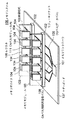
以下、図面を参照し、本発明の実施形態例に基づいて、本発明を更に詳細に説明する。図1は、本発明の一実施形態例のメモリシステムの構成を斜視図として示している。図2は、図1のメモリシステム100のDQバス108方向に沿った断面を示している。メモリシステム100は、メモリコントローラ101と、メモリデバイス104及びレジスタ105を備えるメモリモジュール103と、終端抵抗106とを有する。
【0054】
メモリコントローラ101は、メモリシステム100全体を制御する。メモリモジュール103は、レジスタ105、及び、複数のメモリデバイス104を搭載する。モジュールソケット102は、メモリモジュール103に対応して設けられ、コネクタにより、マザーボード107上の各配線とメモリモジュール103内の配線とを電気的に接続する。メモリコントローラ101は、所定データ長に対応した帯域のDQバス(データバス)108を介してメモリデバイス104に接続し、CAバス(制御系信号バス)109を介してレジスタ105に接続する。
【0055】
CAバス109は、レジスタ105で分岐し、モジュール内CAバス111によって、同じメモリモジュール103内のメモリデバイス104に分配される。DQバス108は、複数の系統が配線され、各DQバス108は、複数のメモリデバイス104を直列に(カスケード)接続する。図1の例では、4系統のDQバス108が配線され、各DQバス108は、4つのメモリデバイス104を直列に接続している(図2)。
【0056】
メモリコントローラ101から出力された信号は、DQバス108及びCAバス109のそれぞれの終端部に配置された終端抵抗106で終端される。また、メモリモジュール103からメモリコントローラ101に向けて出力された信号は、メモリコントローラ101内、或いは、メモリコントローラ101の近傍に設けられた図示しない終端抵抗によって終端される。
【0057】
メモリシステム100内の信号配線は、全て同じインピーダンスとなるように配線され、終端抵抗106には、信号配線の特性インピーダンスに一致する抵抗値が採用される。モジュールソケット102など、局部的に、単独では信号配線とインピーダンスの整合が困難な構成要素が信号配線中に存在する箇所では、その近傍に容量素子などを付加することによって、実効的にインピーダンスが整合される。またメモリは容量負荷に見えるので、その近傍(loaded section)の配線のキャパシタンス成分を低く、又は、インダクタンス成分を高く、つまり、特性インピーダンスを高くすることによって、実効的にインピーダンスが整合される。
【0058】
メモリシステム100では、特にデータバス(DQバス)において信号の反射が生じないようするために、信号配線のインピーダンスを正確に整合させて、高速な読み書きを可能としている。また、高速動作をするシステムにおいては、リターン電流のパスも重要であり、マザーボード107上、或いは、メモリモジュール103上の電源配線についても、不連続が生じないようにする。
【0059】
図2に示すように、メモリモジュールは、モジュール基板122上に複数のメモリデバイス104を備える。各メモリデバイス104は、例えば半田ボールによって構成されるデバイス端子(DQピン)112及びCAピン113を介してモジュール基板122上の対応する配線と電気的に接続する。CAピン113は、メモリデバイス104とモジュール内CAバス111とを接続する。図2の例では、1つのメモリモジュール103には2本のモジュール内CAバス111が配線され、各モジュール内CAバス111は、それぞれに対応するCAピン113を介してメモリデバイス104に制御系信号を供給する。
【0060】
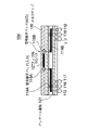
各メモリデバイス104は、1つのパッケージ内DQバス114につき2つのDQピン112を備え、各DQピン112は、モジュール内DQバス110と、パッケージ内DQバス114とを相互に接続する。メモリコントローラ101から終端抵抗106までのデータバスは、DQバス108、モジュール内DQバス110、DQピン112、及び、パッケージ内DQバス114によって分岐箇所がない一筋の配線として構成されている。
【0061】
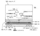
図3は、メモリデバイス104の詳細をメモリチップ120の入出力部分の等価回路と共に示している。メモリデバイス104は、データ記憶部として構成されるメモリチップ120と、メモリチップ120を搭載するパッケージ基板121とを備える。メモリチップ120は、入力ドライバ128と、出力ドライバ129と、入力保護抵抗130と、静電保護容量131と、メモリセルアレイを含む図示しない内部回路とを備える。なお、同図では、制御系信号の配線については省略して図示している。
【0062】
メモリデバイス104は、緩衝材(エラストマ)132を介してモジュール基板122に貼り付けられる。パッケージ基板121は複数の配線層を有し、各配線層には、面状に配線されるパッケージ内電源プレーン(面)118(VDD)及び119(GND)と、パッケージ内DQバス114とがそれぞれ配線される。パッケージ内VDD面118及びGND面119は、それぞれ2つの電源ピン116(VDDピン)117(GNDピン)とビアを介して接続される。パッケージ内DQバス114は、その両端で2つのDQピン112とそれぞれビアを介して接続される。パッケージ内DQバス114は、VDD面118と、GND面119との中間の配線層に配線される。
【0063】
メモリチップ120は、信号入出力パッドとして構成される所定数の信号端子パッド115を備え、各信号端子パッド115は、所定の位置で、対応するパッケージ内DQバス114にビアを介して接続される。入力ドライバ128は、信号端子パッド115から入力保護抵抗130を介して入力する信号を、電圧値を変換するなどしてメモリチップ120の内部回路に出力する。出力ドライバ129は、信号端子パッド115から、所定の電圧値で信号を出力する。このような構成を採用することで、例えば、信号端子バッド115から出力する信号は、1本のパッケージ内DQバス114を介して2つのDQピン112から出力することができる。出力ドライバ129の出力用MOSトランジスタは、静電保護素子としても機能し、MOSトランジスタの寄生容量(静電保護容量)131は、静電気破壊現象から、メモリチップ120の内部回路を保護する。
【0064】
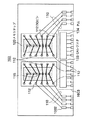
図4は、図1及び図2に示すメモリモジュール103の詳細を示している。メモリモジュール103は、モジュール基板122のメモリコントローラ側及び終端抵抗側の面に、それぞれ図3に示すメモリデバイス(A)、(B)104を搭載している。モジュール基板122は、メモリコントローラ側及び終端抵抗側に、接続端子125A、125Bを備える。接続端子125A、Bは、モジュールソケット102(図1)において、モジュール内DQバス110A、110Bと、マザーボード107上のDQバス108とをそれぞれ接続するための端子として構成される。
【0065】
モジュール基板122は、内部に電源(モジュール内VDD面123及びGND面124)が配線される配線層を有する。モジュール内VDD面123及びGND面124は、メモリデバイス104のVDDピン116、及び、GNDピン117並びにビアを介してパッケージ内VDD面118及びGND面119に接続される。モジュール基板122内の配線層では、基板表面側にそれぞれモジュール内GND面124が配線され、モジュール内GND面124の間にモジュール内VDD面123が配線される。つまり、モジュール内VDD面123は、2つのモジュール内GND面124によって挟み込まれた配線として構成される。メモリデバイス104のVDDピン116及びGNDピン117は、DQピン112の近傍に配置される。
【0066】
モジュール基板122の表面には、モジュール内DQバス110A、110B、及び、CAバス111が配線される。モジュール内DQバス110A、110Bは、それぞれメモリデバイス104のDQピン112及びビアを介してパッケージ内内DQバス114に接続される。配線層を縦断するモジュール内DQバス110Cは、モジュール基板122のメモリコントローラ側の面のDQピン112と、終端抵抗側の面のDQピン112とを接続するビアで構成される。メモリモジュール103では、データバスが、モジュール内DQバス110A、100B、110C、及び、各メモリデバイス104のパッケージ内DQバス114によって、一筋の配線として構成される。
【0067】
ここで、図13に示す従来のメモリシステム200のメモリデバイス204では、図14に示すパッケージ内配線213がモジュール内配線208に対して分岐配線を構成していた。本実施形態例では、1つのパッケージ内DQバス114に対して、2つのDQピン112を備えるため、データバスが上記のような一筋の配線で構成できる。従来のメモリデバイス204(図14)におけるパッケージ内配線213に相当するパッケージ内DQバス114は、メモリシステム100中の一筋のデータバスの一部を構成し、データバスに対して分岐配線となっていない。
【0068】
図1及び図2に示すメモリシステム100において、データの書き込み時には、メモリコントローラ101から出力された信号は、マザーボード107上のDQバス108を伝播し、モジュールソケット102を介して、メモリモジュール103のメモリコントローラ側の接続端子125A(図4)に到達する。メモリモジュール103では、接続端子125Aに接続するメモリコントローラ側のモジュール内DQバス110Aから、メモリデバイス(A)104に、一方のDQピン112を介して、信号を入力する。
【0069】
メモリデバイス(A)104の一方のDQピン112から入力する信号は、パッケージ内DQバス114を伝播し、分岐配線(ビア)126を介して信号端子パッド115に分岐すると共に、他方のDQピン122から出力する。他方のDQピン112から出力する信号は、モジュール基板122を縦断するモジュール内DQバス110Cを介して、終端抵抗側のメモリデバイス(B)104に、一方のDPピン112を介して入力する。
【0070】
メモリデバイス(B)104の一方のDQピン112から入力する信号は、パッケージ内DQバス114を伝播し、分岐配線126を介して信号端子パッド115に分岐すると共に、他方のDQピン122から出力する。つまり、メモリデバイス(A)及び(B)104では、同じ信号が双方の信号端子パッド115に入力する。他方のDQピン112から出力する信号は、終端抵抗側のモジュール内DQバス110Bを介して、終端抵抗側の接続端子125Bに到達する。
【0071】
メモリシステム100では、前述のように、マザーボード107、モジュールソケット102、メモリモジュール103、及びメモリデバイス104の各構成要素における信号配線のインピーダンス、特にデータバスを構成する信号配線の配線インピーダンスは整合が取れており、また、データバスはメモリチップ120への分岐配線126を除いて分岐のない構造としているため、何れの場所についても、発生する信号反射の影響は無視できるほど小さい。メモリコントローラ101が出力する信号は、DQバス108、及び、いくつかのメモリモジュール103を介して、最終的にマザーボード107上の終端抵抗106に到達し、終端抵抗106で終端される(図2)。
【0072】
一方、データの読み出し動作時には、メモリデバイス104側から、メモリコントローラ101へ向けてデータ信号が出力される。メモリチップ120の図示しない出力回路から信号端子パッド115を介して出力されたデータ信号は、分岐配線126を介してパッケージ内DQバス114に到達する。メモリデバイス104からは、一方のDQピン112を介してメモリコントローラ101へ向けてデータ信号が出力されると共に、他方のDQピン112から終端抵抗106に向けてデータ信号が出力される。
【0073】
メモリコントローラに向けて出力されたデータ信号は、DQバス108やメモリモジュール103内の信号配線を経由してメモリコントローラ101に到達する。DQバス108やメモリモジュール103では、データバスのインピーダンスが整合しており、分岐配線126をデータ信号が往復するのに要する時間が、データ信号の立ち上がり時間に比して十分に短くなるように構成することで、データ信号は波形が大きく乱れることなく伝播し、図示しないメモリコントローラ側の終端抵抗で終端される。一方、終端抵抗106に向けて出力されたデータ信号は、上記した書き込み動作時と同様に、インピーダンス整合されたデータバスを反射なく伝播し、終端抵抗106で終端される。
【0074】
本実施形態例では、上記のように、1つのパッケージ内DQバス114に対応して2つのデバイス端子(DQピン112)を設ける。メモリデバイス104では、パッケージ内DQバス114は、2つのDQピン112間で、メモリチップ120上の信号端子バッド115に分岐配線126を介して接続される。このため、メモリデバイス104のパッケージ内DQバス114を、メモリコントローラ101から終端抵抗106に至るデータバスに対して分岐配線として構成せず、データバス中の一部として構成することができる。つまり、メモリシステム100では、一つの信号の信号配線が、インピーダンスの整合の取れた、一筋の配線構造とすることができる。このようなメモリシステム100では、データバスで発生する信号の反射が低く抑えられ、データ信号を品質よく伝播することができ、従来よりも高速動作が可能となる。
【0075】
また、データバス中の各配線は、電源面(VDD面、GND面)によりシールドされる。このため、信号配線からメモリチップ120に侵入するクロストークノイズを遮断できる。また、パッケージ基板121に、パッケージ内VDD面118電源、及び、パッケージ内GND面119を設け、モジュール内配線114がストリップ線路を構成し、パッケージ基板121に占める金属(銅)の割合が高くなっているため、熱の放散がスムーズに行なわれる。このため、メモリチップ120の温度上昇による性能の低下を抑えることができる。
【0076】
メモリシステム100では、データバスの一部がメモリデバイス104内にパッケージ内DQバス114として配線されるため、メモリデバイス104の直下のメモリモジュール103にはデータバス(モジュール内DQバス108)を配線する必要がなくなる。図2に示すように、メモリデバイス104は、端部にDQピン112が配置され、中央部にCAピン113が配置されるが、データバスの一部がメモリデバイス104を経由するため、その箇所でモジュール内配線108が途切れ、CAバス111とはモジュール基板122上で交差しない。
【0077】
従来のメモリシステム200では、DQバス112とCAバス113とが交差する場合には、DQバス112とCAバス113とを異なる配線層に配線する必要があった。本実施形態例では、データバスがパッケージ内DQバス114を経由するため、メモリモジュール103上を図1に示すように長辺方向(左右方向)に配線されるCAバス111との交差が容易になり、パッケージ基板122の配線層を増やす必要がなくなり、配線レイアウトの自由度が増す。このため、CAバス111に大きな配線占有面積を与えることができ、CAバス111で発生する信号タイミングエラーや、信号反射、クロストークノイズを低減することができる。
【0078】
図7は、本発明の第2実施形態例のメモリシステムで使用されるメモリデバイス104の詳細を示している。本実施形態例のメモリデバイス104は、メモリチップ120と、メモリチップ120よりもサイズが大きいパッケージ基板121を備える。パッケージ基板121は、DQピン112や電源ピン116、117などのデバイス端子に対向する面から、ビアを介して接点を取り出し可能に構成される。このため、図7に示すメモリデバイス104を、例えば2段重ねると、2段目のデバイス端子が、1段目のメモリデバイス104に形成される接点と接続し、簡易に積層構造を得ることができる。
【0079】
図8は、上記第2実施形態例のメモリシステムの構成を示している。本実施形態例のメモリシステム100は、1つのメモリモジュール103内で終端されるデータバスを2系統有する点、及び、1つのメモリモジュール103が積層した複数のメモリデバイス104を搭載する点で、第1実施形態例と相違する。なお、同図では、モジュール内の電源面(VDD面123及びGND面124)と、パッケージ内の電源面(VDD面118及びGND面119)との接続については、省略して図示している。
【0080】
データバスは、0系及び1系の2系統が配線される。データバスの各系は、それぞれ、一端をメモリコントローラ101内に設けられたオンチップターミネーション(オンチップ終端抵抗)106Aによって終端され、他端をメモリモジュール103上に設けられた終端抵抗106で終端される。データバスを構成する各DQバス108は、メモリシステム100の各要素に電源を供給する電源面(VDD又はGND)135、136が配線される層に挟まれて配線される。
【0081】
図9は、図8のメモリモジュール103の詳細を示している。メモリモジュール103の片側には2つのメモリデバイス104が積層され、1つのメモリモジュール103は、計4つのメモリデバイス104を有する。モジュール内DQバス110A、110Bは、その一部が、モジュール内VDD面123及びGND面124の中間の配線層に配線される。各メモリデバイス104では、パッケージ内DQバス114と、信号端子パッド115とが分岐配線(ビア)126を介して接続される。接続端子125から終端抵抗106に至るデータバスは、以下のように、一筋の配線として構成される。
【0082】
接続端子125は、メモリコントローラ側のモジュール内DQバス110Aを介してメモリデバイス(B)104の第1のDQピン(B1)112に接続され。DQピン(B1)112は、モジュール内DQバス(B)114に接続されることなく、ビアを介してメモリデバイス(A)104の第1のDQピン(A1)112に接続される。DQピン(A1)112は、ビアを介してモジュール内DQバス(A)114の一端に接続される。
【0083】
メモリデバイス(A)104の第2のDQピン(A2)112は、ビアを介して、モジュール内DQバス(A)112の他端に接続されると共に、モジュール内DQバス(B)112の一端に接続される。モジュール内DQバス(B)114の他端は、ビアを介してメモリデバイス(B)104の第2のDQピン(B2)112に接続される。DQピン(B2)112は、ビアで構成されるモジュール基板122を縦断するDQバス110Cを介して、メモリデバイス(C)104の第1のDQピン(C1)112に接続される。
【0084】
メモリデバイス(C)及び(D)104では、メモリデバイス(B)104の第1のDQピン(B1)112から第2のDQピン(B2)112までの逆順と同様な接続によって、メモリデバイス(C)104の第1のDQピン(C1)112と、第2のDQピン(C2)112とが接続される。DQピン(C2)は、終端抵抗側のモジュール内DQバス110Bに接続され、モジュール内DQバス110Bは、モジュール上に搭載された終端抵抗106によって終端される。
【0085】
図8に示すメモリシステム100において、例えば、0系へのデータの書き込み時には、メモリコントローラ101から出力する信号は、マザーボード107上のDQバス108を伝播し、モジュールソケット102を介して、メモリモジュール103の接続端子125(図9)に到達する。
【0086】
メモリモジュール103に到達した信号は、データバスを構成するDQバス110、114やビアを介し、DQピン112を(B1→A1→A2→B2→C1→D1→D2→C2)と順次に伝播して、終端抵抗106で終端される。メモリコントローラ101から出力された信号は、信号端子パッド115に接続するための分岐配線126以外の箇所では分岐せずに、終端抵抗106に到達し、メモリモジュール103上で終端される。また、信号が、モジュールソケット102を通過する回数は1回となっている。
【0087】
本実施形態例では、第1実施形態例と同様に、メモリコントローラ101から終端抵抗106に至るデータバスが、分岐のない一筋の配線として構成されるため、データ信号の反射が低く抑えられ、品質よく信号伝達ができる。また、1つのメモリモジュール103に複数のメモリデバイス104を積層することで、両々の大きなメモリを少ない面積で実現できる。
【0088】
本実施形態例では、1つの系統のデータバスについて、一度しかモジュールソケット102を通過しない構成を採用する。モジュールソケット102では、容量を付加するなどして、インピーダンス整合を図ることはある程度可能になる。しかし、モジュールソケット102のコネクタ部では、データバスに対して必ずしも適切な位置に電源線(VDD線又はGND線)を配置することが容易ではことが多い。電源線を適切に配置できない場合には、理想的なデータバスを構成することが困難となり、信号伝達特性が劣化する。1つの系統のデータバスが、モジュールソケット102を通過する回数を減らすことで、信号伝達特性が向上する。
【0089】
図10は、本発明の第3実施形態例のメモリシステムで使用されるメモリデバイスの詳細を示している。第1及び第2実施形態例では、メモリチップ120の信号端子パッド115が入出力パッドとして構成されたが、本実施形態例では、信号端子パッド115が、信号を入力する信号端子パッド115Aと、信号を出力する信号端子パッド115Bとに分離される。
【0090】
図3に示すメモリデバイス104では、一方のDQピン112から他方のDQピン112に至るデータバスが、信号端子パッド115に接続する分岐配線126が配線される箇所で、分岐を有する構造を採用したが、本実施形態例では、これに代えて、一方のDQピン112から他方のDQピン112までのデータバスが、分岐を有しない構造を採用する。具体的には、図10に示すように、信号入力端子パッド115Aと信号出力端子パッド115Bとがチップ内DQバス127で接続され、パッケージ内内DQバス114は、一方のDQピン112と信号入力端子パッド115Aとを接続するパッケージ内DQバス114Aと、他方のDQピン112と信号出力端子パッド115Bとを接続するパッケージ内DQバス115Bとに分割される。
【0091】
図11は、図10に示すメモリデバイス104を、メモリチップ120の入出力部分の等価回路と共に示している。メモリチップ120は、入出力部分に、入力ドライバ128、出力ドライバ129、入力保護抵抗130、及び、静電保護容量131を備える。
【0092】
入力ドライバ128は、信号入力端子パッド115Aから入力保護抵抗130を介して入力された信号を、電圧値を変換するなどしてメモリチップ120の内部回路に出力する。出力ドライバ129は、信号出力端子パッド115Bから、所定の電圧値で信号を出力する。出力ドライバ129の出力用MOSトランジスタは、静電保護素子としても機能し、MOSトランジスタの寄生容量(静電保護容量)131は、静電気破壊現象から、メモリチップ120の内部回路を保護する。
【0093】
信号入力端子パッド115Aに信号を入力する場合には、一方のDQピン112から入力する信号は、モジュール内DQバス114A及びビアを介して、或いは、モジュール内DQバス114B、信号出力パッド115B、チップ内DQバス127、及び、ビアを介して信号入力端子パッド115Aに到達する。信号入力端子パッド115Aに到達した信号は、チップ内DQバス127、信号出力パッド115B、モジュール内DQバス114B、及び、ビアを介して、或いは、モジュール内DQバス114A及びビアを介して他方のDQピン112に到達し、メモリデバイス104の外部に出力する。このとき、一方のDQピン112から他方のDQピン112までのパッケージ基板121内の信号経路では、分岐箇所がない。
【0094】
また、メモリチップ120が信号を出力する場合には、信号出力端子パッド11Bから出力する信号は、チップ内DQバス127、信号入力端子パッド115A、モジュール内DQバス114A、ビア、及び、一方のDQピン112を介してメモリデバイス104の外部に出力すると共に、モジュール内DQバス114B、ビア、及び、他方のDQピン112を介してメモリデバイス104の外部に出力する。
【0095】
本実施形態例では、メモリチップ120の信号を入力する信号端子パッド115Aと、信号を出力する信号端子パッド115Bとが異なるパッドとして構成される。この場合、パッケージ基板121では、メモリデバイス104の一方のDQピン112から他方のDQピン112までを、分岐のない一筋の配線で構成することができ、信号伝達特性が更に向上する。
【0096】
なお、上記実施形態例では、メモリデバイス104は、メモリチップ120に、配線層を有するパッケージ基板121を貼り付ける構造を採用したが、パッケージ基板121に代えて、層構造を持つテープ素材などを用いることもできる。また、パッケージ基板121内の各配線のインピーダンスは、配線の厚さや、配線幅、配線間隔、配線層又は絶縁層の物質等、配線の構造等により調整を行なうことができるが、メモリチップ120上の信号端子パッド115の近傍に容量素子を付加するなどして調節することも可能である。
【0097】
図12は、メモリデバイス104の別の例の詳細を示している。上記実施形態例では、パッケージ内DQバス114がパッケージ内VDD面118とGND面119とにはさまれて配線されたが、図12のメモリデバイス104は、メモリチップ側の配線層にパッケージ内VDD面118又はGND面119を配線し、その下層の配線層にパッケージ内DQバス114を配線する。また、第3実施形態例では、入力ドライバが信号入力端子パッド115Aに直接に接続され、出力ドライバが信号出力端子パッド115Bに直接に接続される例を示したが、入力ドライバや出力ドライバは、チップ内配線で接続された2つの信号端子パッド間に配置されていてもよい。
【0098】
図23はメモリシステムにおける入出力信号バスの例である。(a)はSSTLバス、(b)は1対1接続バスの例である。
【0099】
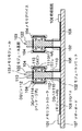
図5は、図23(a)に示す従来のメモリモジュール2302に用いられるメモリモジュール103の配線レイアウトを示している。図6はメモリモジュール2302と同様に用いるメモリモジュール103の配線レイアウトを示している。図5に示すように、従来のメモリモジュール203では、モジュール基板上のコネクタ位置関係の制約や、モジュール基板上に配置されたCAレジスタ133やPLL回路134等のブロックが存在することより、配線の引き回しが複雑になって、モジュール内DQバス208の配線長を均一化することが困難な場合があった。
【0100】
本実施形態例では、一つの信号に対して2つのデバイス端子があるため、図6に示すように、2つのDQピン112のうち、何れか一方のDQピン112を利用することにより、適正な配線レイアウトを容易に作ることができ、また配線長の均一化を容易にすることができる。また図23(b)に示すメモリモジュール2303に対しても、同様に図22に示すメモリモジュールの配線レイアウトのようにすれば、適正な配線レイアウトを容易に作ることができ、また配線長の均一化を容易にすることができる上、メモリデバイス104の一方のDQピン112から他方のDQピン112までを、分岐のない一筋の配線で構成することができ、良好な信号伝達特性が得られる。
【0101】
図15は本発明の第3の視点によるメモリパッケージの例である。メモリパッケージの左右両側に1つずつ入出力信号端子1505〜1508があり、チップ1509上の入出力信号用チップパッドから左右どちらかの入出力信号端子に配線されている。例えば(a)のパッケージ1501では入出力信号用チップパッド1503は左側の入出力端子1508へ、また(b)のパッケージ1502では入出力信号用チップパッド1503は右側の入出力端子1508へ配線されている。
【0102】
図16は本発明の第3の視点によるメモリパッケージを用いたメモリモジュールの例である。図16に示すように配線できない領域1603の左側からメモリへの配線する場合は左の端子が有効なパッケージ1501を使い、逆に配線できない領域1603の右側からメモリへ配線する場合は右の端子が有効なパッケージ1502を使っている。このように2種類のパッケージ1501、1502のうち、何れか一方のパッケージを用いることにより、適正な配線レイアウトを容易に作ることができ、また配線長を短く均一化することが容易にできる。
【0103】
図17は図16のメモリモジュールに用いられるメモリパッケージの別の実施例である。このメモリパッケージはメモリパッケージの左右両側に1つずつ入出力信号端子が有し、入出力信号用チップパッドの左右両側の近傍にパッドを有する。そして該入出力信号端子と入出力信号用チップパッドの近傍のパッドの間が配線され、左右何れかのチップパッドの近傍のパッドと入出力信号用チップパッドの間がワイヤボンディングで接続されている。例えば入出力信号端子1508とチップパッド左側近傍のパッド1703の間が配線されており、パッド1703と入出力信号用チップパッド1503の間はボンディングワイヤ1702で接続されることでパッケージの左側に有効な入出力信号端子を有する図15(a)と同様のメモリパッケージを構成できる。
【0104】
図18は図16のメモリモジュールに用いられるメモリパッケージの別の実施形態例である。これは図17のメモリパッケージのワイヤボンディングの代わりにジャンパチップを使ったものである。本パッケージはパッケージ基板1804の裏面に端子とチップを有し、表面に配線及びジャンパパッドペア、ジャンパチップを有している。図17のメモリパッケージと同様にパッケージ左右両側に端子を有し、左右両側の端子から入出力信号用チップパッドに配線されているが、配線は途中のジャンパチップ用パッドペア1803で分断されている。そして例えば左側のジャンパチップ用パッドペアをジャンパチップ1802で接続することにより、パッケージの左側に有効な入出力信号端子を有するパッケージを構成できる。なお上記と逆にパッケージ表面にチップ、裏面に配線及びジャンパパッドペア、ジャンパチップを配置しても構わない。
【0105】
図19は図16のメモリモジュールに用いられるメモリパッケージの別の実施形態例である。このメモリパッケージは図17のメモリパッケージと同様にパッケージ左右両側に端子を有し、左右両側の入出力信号端子から入出力信号用チップパッドに配線されている。そして右側の入出力信号端子からの配線は入出力信号用チップパッド近傍1902で切断されている。これにより、パッケージの左側に有効な入出力信号端子を有するパッケージを構成できる。
【0106】
以上、パッケージの左側に有効な入出力信号端子を有するメモリパッケージについて述べたが、パッケージの右側に有効な入出力信号端子を有するメモリパッケージも同様に実現可能であることは言うまでもない。またパッケージ内に電源GND層を設け、配線を伝送線として形成しても良い。
【0107】
図20は図16のメモリモジュールに用いられる第4の視点によるメモリパッケージの実施例(断面図)である。このメモリパッケージ2000は(a)に示すように主にパッケージ基板1804とメモリチップ1503、入出力信号端子2001及び2002からなり、前記パッケージ基板1804の裏面にチップを有し、前記パッケージ基板1804の左右表裏に入出力端子を有している。このうちパッケージ左側の表裏面で対向して配置されている入出力端子2001及び2002はビアホール2003を介して接続されている。
【0108】
またメモリチップ1509の入出力信号用パッド1503から入出力端子2001及び2002にパッケージ内配線1504を用いて接続されている。なおパッケージ内に電源GND層を設け、パッケージ内配線を伝送線として形成しても良い。このように本メモリパッケージの左右いずれかの側に表裏両面に共通の入出力端子を有するので、(b)に示すようにパッケージ2000はメモリモジュール1601に実装する際、表向きに実装した場合はパッケージの左側に有効な入出力信号端子を有するパッケージとして使用でき、裏向きに実装した場合はパッケージの右側に有効な入出力信号端子を有するパッケージとして使用できる。なお、本メモリパッケージは図21(a)に示すようにパッケージ基板1804の両面にメモリチップ1509を実装してもよい。また図21(b)に示すようにパッケージの入出力信号端子に用いられているボール2101を介して積層構造にしても良い。
【0109】
図24は1対1接続バスと一筆書き接続バスを併用しているメモリシステムの例である。メモリ装置2401はメモリコントローラ2405の左右両側に複数のメモリ2403を持ち、前記メモリコントローラ2405と複数のメモリ2403を結ぶ1対1接続バス2406及び一筆書き接続バス2407を有している。ここで1対1接続バスはデータ信号バスやデータストローブ信号に、一筆書き接続バスはコマンド・アドレス信号やクロック信号に使用する事ができる。または1対1接続バスはクロック信号に、一筆書き接続バスはデータ・コマンド・アドレス信号に使用する事もできる。
【0110】
図25は図24記載のメモリ装置に用いる積層メモリ2501の実施例である。(a)はメモリ2501の平面図である。(b)は本メモリの配線領域2504の断面図である。(c)は本発明の配線領域2503の断面図である。本メモリは本発明の第1及び第4の視点の両方を取り入れた半導体ユニットである。本メモリは図21(a)記載のメモリにおいて、配線領域2503で本発明の第1の視点による半導体ユニットと同じくしたものであり、チップパッド1503は半導体ユニットの左右両側の端子2505に配線されている。また配線領域2504は本発明の第4の視点による半導体ユニットと同じくしたものであり、チップパッド1503は半導体ユニットの片側(左)の端子2506に配線されている。端子2505は図25記載のメモリ装置の一筆書き接続バス2407用端子に用いればよい。端子2506は1対1接続バス2406用端子に用いればよい。
【0111】
図26は図25のメモリを図24記載のメモリに適用した例である。図26(a)は1対1接続バス2406に関する断面図である。図の様に1対1接続バス2406は基板内層に形成されている。そしてメモリコントローラ2405の右側に置かれたメモリ2501の1対1接続バス用信号端子2506がメモリのメモリコントローラに近い側(左側)にあるので、メモリのチップパッドまで短い距離で配線できる。またメモリコントローラ2405の左側に置かれたメモリ2501は裏返して実装されている。これによりメモリ2501の1対1接続バス用信号端子2506がメモリコントローラ2405に近い側(右側)になり、メモリのチップパッドまで短い距離で配線できる。
【0112】
(b)は一筆書き接続バス2407に関する断面図である。一筆書き接続バス2407は基板表層に形成され、メモリ2501の左右両側にある一筆書き接続バス用端子に接続されており、メモリ内の配線を介してメモリコントローラ2405から終端抵抗2404まで一筋の配線を構成している。以上の説明でメモリ2501は図21(a)記載のメモリを改造したものであったが、図27のように図21(b)記載のメモリを同様に改造したものでも構わない。また配線は伝送線で構成されているが、図においてグランドプレーンや電源プレーンの記載は省略されている。なお、メモリシステム2401はメモリモジュールとして構成可能であることは言うまでもない。
【0113】
図28は本発明における半導体デバイスの別の実施例である。これは図25に示した半導体デバイスを半田ボールを介して積層したもので4個の半導体チップを実装するものである。(a)は下層のデバイスに接続される1対1接続バスの配線を示す半導体デバイスの断面図である。本デバイスは下層のプリント基板2801及び上層のプリント基板2802から構成されている。下層のプリント基板2801の表面に半導体チップ2804、裏面に半導体チップ2803及びデバイス端子2809を有しており、半田ボール2811とデバイス端子2809はビアホール2810で電気的に接続されている。また上層のプリント基板2802の表面に半導体チップ2806及びデバイス端子2813、裏面に半導体チップ2805を有しており、デバイス端子2813と半田ボール2811はビアホール2812で電気的に接続されている。下層のプリント基板2801においては配線2812がビアホール2810と半導体チップ2803のチップパッド2807並びに半導体チップ2804のチップパッド2808に接続されている。ここで半導体チップ2803のチップパッド2807と半導体チップ2804のチップパッド2808はビアボールで接続され、このビアホールと配線2812が接続されている事が望ましい。
【0114】
(b)は上層のデバイスに接続される1対1接続バスの配線を示す断面図である。下層のプリント基板2801の裏面にデバイス端子2821を有しており、半田ボール2823とデバイス端子2821はビアホール2822で電気的に接続されている。また上層のプリント基板2802の表面にデバイス端子2825を有しており、デバイス端子2825と半田ボール2823はビアホール2824で電気的に接続されている。上層のプリント基板2802においては配線2826がビアホール2824と半導体チップ2805のチップパッド2827並びに半導体チップ2806のチップパッド2828に接続されている。ここで半導体チップ2805のチップパッド2827と半導体チップ2806のチップパッド2828はビアボールで接続され、このビアホールと配線2826が接続されている事が望ましい。
【0115】
(c)は上層及び下層のデバイスに並列的に一筆書き接続される配線を示す半導体デバイスの断面図である。下層のデバイスの裏面にはデバイス端子2831及び2842が、表面には半田ボール2833及び2844があり、半田ボール2833とデバイス端子2831はビアホール2832で、また半田ボール2844とデバイス端子2842はビアホール2843で電気的に接続されている。そして下層のプリント基板2801の配線2838はビアホール2832、半導体チップ2803のチップパッド2836及び半導体チップ2804のチップパッド2837、ビアホール2843を一筆書き接続している。ここでチップパッド2836、2837は下層のプリント基板2801のビアホールで接続されている事が望ましい。上層のデバイスの表面にはデバイス端子2835及び2846が、裏面には半田ボール2833及び2844があり、半田ボール2833とデバイス端子2835はビアホール2834で、また半田ボール2844とデバイス端子2846はビアホール2844で電気的に接続されている。
【0116】
そして、上層のプリント基板2802の配線2839はビアホール2834、半導体チップ2805のチップパッド2840及び半導体チップ2806のチップパッド2841、ビアホール2845を一筆書き接続している。ここでチップパッド2840、2841は下層のプリント基板2802のビアホールで接続されている事が望ましい。また応力的・熱的観点から半導体チップ2804と2805の間には緩衝材を挟む事が望ましい。また本積層デバイスをメモリモジュール上に実装した際、上層デバイスの剥き出しになっているデバイス端子2813、2835、2846に絶縁体を被せて外部との短絡から保護するか、もしくは除去する事が望ましい。さらに半導体デバイス配線の実効的特性インピーダンスとデバイス端子に接続される配線の特性インピーダンスとの整合のために、配線2838及び2839の長さl、単位長さ当たりのインダクタンスL0、単位長さ当たりのキャパシタンスC0、半導体チップのチップパッドにおける負荷容量Cin、デバイス端子に接続される配線の特性インピーダンスZMBの間に数1式の関係が成り立っている事が望ましい。
【0117】
【数1】

【0118】
【発明の効果】
以上説明したように、本発明の半導体ユニット、及び、半導体モジュール、並びに、このような半導体ユニットや半導体モジュールを備えるメモリシステムでは、半導体ユニットは1つの信号配線に対して2つの外部端子を備える。例えば、この半導体ユニット及び半導体モジュールを使用したメモリシステムでは、信号配線が一筋の配線として構成され、半導体ユニット内で発生する信号反射を低く抑えることができ、高速動作が可能となる。また、信号配線が電源配線層よりシールドされる構成を採用すると、半導体チップに侵入するノイズが減少してクロストークの影響が低くなり、また、パッケージ基板に占める金属の割合が高くなるため、熱の放散がスムーズに行なわれて、半導体チップの温度上昇による性能の低下を抑えることができる。
【0119】
また、SSTLバスのようにメモリモジュールコネクタで信号配線の分岐を持つメモリシステムにおいても、半導体モジュールにおいて配線長が短くなるように、半導体ユニットの前記2つの外部端子のうち一方の外部端子を配線先として選択できるので、半導体モジュール内で発生する信号反射を低く抑えることができ、高速動作が可能となる。
【図面の簡単な説明】
【図1】本発明の一実施形態例のメモリシステムの構成を示す斜視図である。
【図2】図1のメモリシステム100のDQバス108方向に沿った断面図である。
【図3】メモリデバイス104の詳細をメモリチップ120の入出力部分の等価回路と共に示した断面図である。
【図4】図1及び図2に示すメモリモジュール103の詳細を示す断面図である。
【図5】従来のメモリモジュール203の配線レイアウトを示す平面図である。
【図6】図1に示すメモリモジュール103の配線レイアウトを示す平面図である。
【図7】本発明の第2実施形態例のメモリシステムで使用されるメモリデバイス104の詳細を示す断面図である。
【図8】本発明の第2実施形態例のメモリシステムの構成を示す断面図である。
【図9】図8のメモリモジュール103の詳細を示す断面図である。
【図10】本発明の第3実施形態例のメモリシステムで使用されるメモリデバイスの詳細を示す断面図である。
【図11】図10に示すメモリデバイス104を、メモリチップ120の入出力部分の等価回路と共に示す断面図である。
【図12】メモリシステム100におけるメモリデバイス104の別の例の詳細を示す断面図である。
【図13】従来のメモリシステムにおける信号配線経路を示す断面図である。
【図14】図13のメモリデバイス204の詳細を示す断面図である。
【図15】本発明の第3の視点の半導体ユニットの第1実施形態例のメモリパッケージの構成を示す平面図である。
【図16】本発明の第3の視点の半導体モジュールの構成を示す平面図である。
【図17】本発明の第3の視点の半導体ユニットの第2実施形態例のメモリパッケージの構成を示す平面図である。
【図18】本発明の第3の視点の半導体ユニットの第3実施形態例のメモリパッケージの構成を示す平面図である。
【図19】本発明の第3の視点の半導体ユニットの第4実施形態例のメモリパッケージの構成を示す平面図である。
【図20】本発明の第4の視点の半導体ユニットの第1実施形態例のメモリパッケージの構成を示す断面図である。
【図21】本発明の第4の視点の半導体ユニットの第2実施形態例のメモリパッケージの構成を示す断面図である。
【図22】本発明の第1及び第2の視点の半導体ユニットを1対1接続バスに用いられるメモリモジュールに用いた場合の実施例を示す図である。
【図23】従来の別のメモリシステムにおける信号配線経路を示す断面図である。
【図24】1対1接続バスと一筆書き接続バスを併用したメモリシステムの構成を示すブロック図である。
【図25】本発明の第1及び第4の視点を兼ね備えた積層メモリの第1の実施例の平面図及び断面図である。
【図26】本発明の第1及び第4の視点を兼ね備えたメモリの第1の実施例を用いた1対1接続バスと一筆書き接続バスを併用したメモリ装置の断面図である。
【図27】本発明の第1及び第4の視点を兼ね備えた積層メモリの第2の実施例の断面図である。
【図28】本発明の第1及び第4の視点を兼ね備えた4つのデバイスを搭載した積層メモリの実施例の断面図である。
【符号の説明】
100,200:メモリシステム
101,201:メモリコントローラ
102,202:モジュールソケット
103,203:メモリモジュール
104,204:メモリデバイス
105:レジスタ
106,205:終端抵抗
107,206:マザーボード
108:DQバス
109:CAバス
110:モジュール内DQバス
111:モジュール内CAバス
112,209:DQピン(デバイス端子)
113:CAピン
114:パッケージ内DQバス
115,212:信号端子パッド
116,117:電源ピン(VDDピン、GNDピン)
118,119:パッケージ内電源面(VDD面、GND面)
120,210:メモリチップ
121,211:パッケージ基板
122:モジュール基板
123,124:モジュール内電源面(VDD面、GND面)
125:接続端子
126:分岐配線
127:チップ内DQバス
128:入力ドライバ
129:出力ドライバ
1501:半導体ユニット左用
1502:半導体ユニット右用
1503:チップパッド
1504:パッケージ内配線
1505,1506,1507,1508:入出力信号端子
1509:チップ
1601:メモリモジュール
1602:スタブ抵抗
1603:メモリへの配線禁止領域
1604:メモリモジュール端子
1605:メモリへの配線
1701:パッケージ左用
1702:ボンディングワイヤ
1703:ボンディングパッド
1801:パッケージ左用
1802:ジャンパチップ
1803:ジャンパチップ用パッド
1804:パッケージ基板
1901:パッケージ左用
1902:切断された配線
2000:左右兼用パッケージ
2001,2002:入出力信号端子
2003:ビアホール(スルーホール)
2101:半田ボール
2102:追加されたメモリ
2201:終端抵抗
2202:終端電位プレーンへのビアホール
2301:スタブ抵抗
2302:メモリモジュール
2303:1対1接続メモリモジュール
2401:メモリ装置
2403:メモリ
2404:終端抵抗(網)
2405:メモリコントローラ
2406:1対1接続バス
2407:一筆書き接続バス
2408:メモリ装置入出力信号バス
2501:積層メモリ
2503:一筆書き接続信号用配線
2504:1対1接続信号用配線
2505:一筆書き接続信号端子
2506:1対1接続信号端子
2601:終端電位プレーン
2801,2802:プリント基板
2803,2804,2805,2806:半導体チップ
2807,2808:チップパッド
2809,2813,2821,2825,2831,2835、2842,2846:デバイス端子
2810,2812,2822,2824,2832,2834,2836,2837,2840,2841,2843,2845:ビアホール
2811,2823,2833、2844:半田ボール
2826,2838,2839:パッケージ内配線[0001]
TECHNICAL FIELD OF THE INVENTION
The present invention relates to a semiconductor unit, a semiconductor module, and a memory system, and more particularly to a semiconductor unit, a semiconductor module, and a memory system in which a data signal or the like is less deteriorated during high-speed operation.
[0002]
[Prior art]
In recent years, memory systems have been increasingly required to operate at higher speeds. In particular, high-speed memory systems are required to have performances corresponding to high frequencies such as several hundred MHz to several GHz. In general, in a memory system, when an operating frequency is increased, a waveform is likely to be disturbed when a signal propagates through a wiring. Therefore, as in the memory systems described in Patent Documents 1 to 3, a signal is transmitted to a signal wiring at a high speed. It is designed to be propagated accurately.
[0003]
For example, Patent Literature 1 describes a technique for reducing the number of signal wiring branches and reducing the reflection of signals generated at the wiring branches as a memory system capable of high-speed operation. FIG. 13 shows a signal wiring path in the memory system described in FIG. 21 of Patent Document 1. The
[0004]
The
[0005]
The
[0006]
FIG. 14 shows details of the
[0007]
The
[0008]
As described above, according to the technology described in Patent Document 1, in the
[0009]
Patent Document 3 describes an example of a memory bus with an SSTL interface standardized by JEDEC (a subordinate organization of the Electronic Industries Association of the United States) as a memory system capable of high-speed operation (SSTL: Stub Series Terminated Logic). . The SSTL bus is provided with a terminating resistor at at least one end of the bus line, and a resistor (stub resistor) for matching the characteristic impedance of the transmission line at a branch point of the signal line, so that the SSTL bus occurs at a branch of the line. To reduce signal reflections.
[0010]
FIG. 20 of Patent Document 3 describes an example of an SSTL bus having terminal resistors at both ends of a bus line. FIG. 23A shows an embodiment of the SSTL bus. As shown in the figure, in the SSTL bus, when connecting the
[0011]
In this case, when the signal reflected at the end of the branch line returns to the main line, reflection of the signal is reduced because the impedance mismatch between the branch line and the main line is reduced. Therefore, disturbance of the waveform due to repetition of reflection can be reduced, and high-speed data transfer can be performed. Further, the terminal of the main line is terminated to a predetermined terminal voltage (for example, half of the power supply voltage) via the
[0012]
As described above, in the technology described in Patent Document 3, in a memory system having a branch that performs high-speed operation, a resistor (stub resistor) for matching the characteristic impedance of a transmission line is provided at a branch point of a signal line. High-speed operation is enabled by reducing signal disturbance due to repeated signal reflection occurring at the wiring branch point.
[0013]
[Patent Document 1]
JP 2001-256772 A
[0014]
[Patent Document 2]
JP 2001-68617 A
[0015]
[Patent Document 3]
JP-A-10-020974
[0016]
[Problems to be solved by the invention]
As described above, in the
[0017]
For example, if the wiring length of the wiring 213 in the package is 10 mm and the propagation time per unit distance of the signal propagating in the wiring is 6 ns / m, the time tS required for the signal to reciprocate through the wiring 213 in the package is 120 ps. Become. When the rise time tR of the propagating signal is less than about twice the signal round trip time tS, the influence on the signal waveform increases, and the disturbance of the waveform due to signal reflection becomes apparent. Assuming that the signal rising time tR is about 1/10 of the operating frequency, the signal rising time tR when the operating frequency is 100 MHz is about 1 ns, and the signal rising time tR is about 100 ps when the operating frequency is 1 GHz. When the operating frequency is about 100 MHz, the signal reciprocating time tS is sufficiently shorter than the rise time tR, and the disturbance of the waveform does not cause a serious problem. However, as the operating frequency approaches the GHz order, the signal reciprocating time tS And the rise time tR becomes small, and the disturbance of the signal waveform becomes a problem.
[0018]
In order to realize a stable high-speed operation in the
[0019]
Patent Literature 2 describes a technique of stacking a plurality of semiconductor elements on one memory module. In the technique described in Patent Document 2, signal wiring parallel to the substrate connecting one end and the other end of the substrate formed immediately below the semiconductor element, and alternately arranged at one end and the other end of the substrate. The signal wiring in the stacking direction formed by the via is configured as a single wiring, and corresponds to a high-speed operation. However, in Patent Document 2, the signal wiring in the direction parallel to the substrate passes through a long section immediately below the semiconductor element, and when the operating frequency increases, the signal wiring crosses the signal wiring and the power supply wiring in the semiconductor element. There is a problem that the talk noise (electromagnetic coupling noise) gets on. Further, when the semiconductor elements are stacked, heat generated from the semiconductor elements concentrates, causing a problem that the temperature of the module is increased and the performance is reduced.
[0020]
In a memory module that operates at high speed, it is necessary to control the timing of various signals reaching the device with high accuracy. In order to perform timing control with high precision and to lay both data wiring and command address wiring without problems from the viewpoint of timing errors, signal reflection, crosstalk, etc., the wiring occupation area on the layout increases, Degree of freedom decreases. In particular, in command address wiring, it is necessary to distribute signals from the registers mounted in the memory module to all memory devices, and the number of command address wires increases due to module miniaturization, large memory chip capacity, and expanded functions. Due to such requirements, the wiring occupation area is further increased, the degree of freedom of the wiring is reduced, and the layout becomes more severe.
[0021]
Further, in the conventional memory module, there are restrictions on the positional relationship between the terminals on the module substrate to be wired and the corresponding terminals on the memory device, and the command / address signal register IC or the clock buffer disposed on the module substrate. Due to restrictions on a non-wiring area such as a PLLIC (PLL: Phase-Locked Loop), routing of signal wiring from a memory module terminal to a memory device terminal is complicated, and the wiring length of the signal wiring may be increased. In a memory system having a branch for performing signal transmission on the order of several hundred MHz, the above-mentioned signal wiring corresponds to a branch wiring, and an increase in the wiring length increases disturbance of a signal waveform generated by reflection and reciprocation of a signal in the branch wiring. There was a problem.
[0022]
The present invention solves the above problems, shortens the wiring length of branch wiring in a package or a memory module in a memory system, and ensures that signal waveform disturbance does not cause a problem in operation of the memory system even during high-speed operation. It is an object of the present invention to provide a semiconductor unit and a semiconductor module which alleviate the lack of freedom and a memory system including such a semiconductor unit and a semiconductor module.
[0023]
Further, the present invention provides a semiconductor unit, a semiconductor module, and a memory system that can reduce crosstalk noise on a memory device from signal wiring, improve heat dissipation capability, and suppress device performance degradation due to device temperature rise. Aim.
[0024]
[Means for Solving the Problems]
In order to achieve the above object, a semiconductor unit according to a first aspect of the present invention is a semiconductor unit having two device terminals for one input / output signal, wherein the semiconductor unit includes a signal wiring layer and a power supply. Or a multilayer substrate having at least two wiring layers including a ground wiring layer, and a semiconductor chip having input / output pads and mounted on the surface of the multilayer substrate via the input / output pads. One device terminal is disposed on the laminated substrate and connected to both ends of one signal line in the signal wiring layer, and the one signal line is connected to an input / output of the semiconductor chip via a via hole. It is characterized by being connected to a pad.
[0025]
In a semiconductor unit according to a first aspect of the present invention, two device terminals are provided corresponding to one input / output signal, and each device terminal is provided with a signal wiring routed on a signal wiring layer of a laminated substrate (package substrate). Connected to each other. The signal line is connected to the input / output pad of the corresponding semiconductor chip via a via (through hole) at a desired position. When viewed from both device terminals, the wiring (via) connected to the input / output pad forms a branch wiring with respect to the signal line formed between the device terminals. Since two device terminals are provided corresponding to one input / output signal, the semiconductor unit inputs a signal input from one device terminal to the semiconductor chip via an input / output pad via a branch wiring, and inputs the other device terminal. It can be taken out from the terminal. Therefore, for example, instead of branching from a data bus formed outside and inputting a signal to the semiconductor unit, a signal line formed in the semiconductor unit can be inserted into the data bus.
[0026]
In the conventional structure in which one input / output pad is connected to one device terminal, the signal wiring in the semiconductor unit from the device terminal to the input / output pad forms a branch line for the data bus. In the present invention, a wiring from a signal wiring connecting between two device terminals to an input / output pad of a semiconductor chip constitutes a branch line. Compared with the conventional semiconductor unit, the wiring length of the wiring constituting the branch line with respect to the data bus can be shortened, and the time for a signal to reciprocate on the branch line is shortened. The influence of the signal reflection caused by the above on the signal waveform is small, and the operation of the semiconductor unit does not become unstable.
[0027]
The package substrate has at least two wiring layers, and a power supply surface (for example, a VDD surface) and a ground surface (GND surface) are wired on the power supply wiring layer. By shielding the signal wiring layer with the power supply wiring layer, crosstalk invading the semiconductor chip from the input / output signal lines can be reduced. It is preferable that the branch wiring is substantially composed of only a via hole.
[0028]
A semiconductor unit according to a second aspect of the present invention is a semiconductor unit including two device terminals for one input / output signal, and the semiconductor unit includes at least a signal wiring layer and a power supply or ground wiring layer. A multilayer substrate having two wiring layers; and a semiconductor chip having input / output pads and mounted on the surface of the multilayer substrate via the input / output pads. And two device terminals are connected to the two input / output pads via corresponding signal wirings and via holes in the signal wiring layer, respectively. And
[0029]
A semiconductor unit according to a second aspect of the present invention includes two device terminals corresponding to one input / output signal, and each device terminal includes two input / output pads corresponding to one input / output signal. It is connected to each input / output pad of the chip via signal wiring. In a semiconductor chip, each input / output pad is connected to each other by a wiring in the chip, and a signal line formed between both device terminals is configured as a single wiring. For example, when a signal is input from a data bus formed outside to one of the input / output pads of the semiconductor chip, the input signal is input to the semiconductor chip from one of the input / output pads, the wiring inside the chip, and the other input / output pad. The signal is output from the other device terminal via the output pad.
[0030]
For this reason, the wiring length of the wiring constituting the branch line with respect to the data bus can be further reduced, and the time for a signal to reciprocate on the branch line is further reduced. And the operation of the semiconductor unit does not become unstable. The package substrate has at least two wiring layers, and a power supply surface (for example, a VDD surface) and a ground surface (GND surface) are wired on the power supply wiring layer. By shielding the signal wiring layer with the power supply wiring layer, crosstalk that enters the semiconductor chip from the input / output signal lines can be reduced.
[0031]
A semiconductor unit according to a third aspect of the present invention is a semiconductor unit provided with two device terminals in the semiconductor unit for one input / output signal, wherein the semiconductor unit includes at least one of a semiconductor chip and the semiconductor chip. The semiconductor device is characterized by comprising a wiring for selectively connecting one input / output signal chip pad and one device terminal electrically connected to the semiconductor module among two device terminals corresponding to the chip pad.
[0032]
The semiconductor unit according to the third aspect of the present invention includes two device terminals corresponding to one input / output signal, and can select a device terminal electrically connected to the semiconductor module. Therefore, it is possible to select and wire a device terminal having a shorter wiring length on the semiconductor module. Also, since there is no wiring between the chip pad and the other device terminal having no electrical connection with the semiconductor module among the two device terminals corresponding to the chip pad, there is no extra wiring capacitance or wiring inductance. . Thereby, signal reflection can be reduced.
[0033]
A semiconductor unit according to a fourth aspect of the present invention is a semiconductor unit provided with two device terminals in the semiconductor unit for one input / output signal, wherein the semiconductor unit includes at least one of a semiconductor chip and the semiconductor chip. The semiconductor device is characterized in that the two device terminals connected to the one input / output signal chip pad are provided one by one facing the front surface and the back surface of one side of the semiconductor unit.
[0034]
In a semiconductor unit according to a fourth aspect of the present invention, a semiconductor terminal is provided with one device terminal in opposition to one of the front and back surfaces of one side of the semiconductor unit corresponding to one input / output signal, and the semiconductor unit is mounted on a semiconductor module. The location of the device terminals can be changed when the front surface of the semiconductor unit faces upward and when the rear surface faces upward. For this reason, it is possible to select and mount a mounting method that can shorten the wiring length on the semiconductor module. Further, since the length of the wiring between the chip pad and the other of the two device terminals corresponding to the chip pad and having no direct connection with the memory module is less than the thickness of the semiconductor unit, Extra wiring capacitance and wiring inductance due to wiring to device terminals that are not directly connected to the module are also very small. Thereby, signal reflection can be reduced.
[0035]
In the semiconductor units according to the first and second aspects of the present invention, the signal wiring layer forms a microstrip line together with a ground wiring layer in the laminated substrate, and the ground wiring layer is formed of the signal wiring layer and the semiconductor. The signal wiring layer may be disposed between a power supply layer and a ground wiring layer in the laminated substrate to form a strip line with the power supply layer or the ground wiring layer. May be. In these cases, the proportion of metal contained in the package substrate in the vicinity of the semiconductor chip increases, so that heat can be smoothly dissipated, and the operation of the semiconductor chip can be prevented from becoming unstable due to a rise in temperature. .
[0036]
In the semiconductor unit according to the first and second aspects of the present invention, the laminated substrate is formed to be larger than a plane size of the semiconductor chip, and faces the two device terminals formed on the back surface of the laminated substrate. Then, a configuration further including two device terminals formed on the surface of the laminated substrate can be adopted. In this case, the semiconductor unit has a maximum of four device terminals for one input / output signal. When the semiconductor units are stacked, two device terminals of one and the other on the front side and one and the other on the back side can be combined and connected to the same input / output signal. . The semiconductor unit may include a device terminal that is not connected to the signal wiring but directly connects the front side and the back side via a via.
[0037]
In a semiconductor unit according to a first aspect of the present invention, the semiconductor chip has at least one of an input buffer and an output buffer, an input protection resistor, and an input / output circuit having an electrostatic protection element corresponding to the input / output pad. Can be adopted.
[0038]
In a semiconductor unit according to a second aspect of the present invention, the semiconductor chip has at least one of an input buffer and an output buffer, an input protection resistor, and an electrostatic protection element corresponding to the two input / output pads. It is possible to adopt a configuration in which one input / output circuit is provided, and the input / output circuit is connected to the one internal wiring via another internal wiring.
[0039]
The semiconductor unit according to the first and second aspects of the present invention is configured to operate by inputting a clock signal, and a distance L between the input / output circuit and the one signal wiring is determined by a product specification of the semiconductor unit. It is preferable that the relationship of 2 × 2L × 7 ns / m <tck / 10 is satisfied with the determined cycle time tck of the clock. In general, assuming that the signal rise time is tR and the time for a signal to reciprocate in the branch wiring is tS, the signal rise time tR is less than twice the signal reciprocation time tS, in other words, the signal reciprocation time tS is equal to the signal rise time tR. When is greater than or equal to, the disturbance of the signal waveform becomes apparent. When the time required for a signal to propagate through a unit distance is 6 to 7 (ns / m) and the signal rise time tR is about 1/10 of the cycle of the operation clock, 2 × 2L × 7 ns / If the relationship of m <tck / 10 is satisfied, the signal waveform disturbance does not affect the operation of the semiconductor unit, and good operation can be performed.
[0040]
A semiconductor module according to the present invention includes a module substrate including a connector and an internal wiring connected to the connector, and a plurality of semiconductor units mounted on the front and back surfaces of the module substrate and connected to the internal wiring. A semiconductor module, wherein each of the semiconductor units is configured as the first or second semiconductor unit of the present invention, and the two semiconductor units of the two semiconductor units arranged opposite to the front and back surfaces of the module substrate. One of the two device terminals is connected to each other via a via hole, and the other of the two device terminals is connected to the connector via an internal wiring disposed on the front and back surfaces of the module substrate, respectively. It is characterized by.
[0041]
In the semiconductor module according to the first aspect of the present invention, the wiring outside the module and the wiring inside the module are respectively connected by connectors on the front surface and the back surface of the module substrate, and the wiring inside each module is mounted on the front surface and the back surface of the module substrate. It is connected to one device terminal of the semiconductor unit of the first or second viewpoint, respectively. The other device terminal of each of the semiconductor units mounted on the front surface and the back surface is connected via a via connecting the front surface and the back surface of the module substrate. For this reason, the wiring from the connector on the front side to the connector on the back side can be configured as a single line, and the number of branching points can be reduced to enable high-speed operation. In addition, immediately below the semiconductor unit, it is not necessary to wire the wiring in the module corresponding to the signal input to the semiconductor unit. Therefore, it is possible to arrange other wiring such as control wiring directly below the unit without increasing the number of wiring layers. The degree of freedom in wiring layout is improved.
[0042]
A semiconductor module according to a second aspect of the present invention includes a module substrate including a connector and an internal wiring connected to the connector, and a front surface mounted on the front and back surfaces of the module substrate and connected to the internal wiring. And a plurality of semiconductor units on which a device terminal can be formed on the back surface, wherein the plurality of semiconductor units are stacked, and a device terminal formed on the back surface of the upper semiconductor unit and a lower semiconductor unit. The device terminal is connected to a device terminal formed on the surface.
[0043]
In the semiconductor module according to the second aspect of the present invention, the wiring in the module is connected to one of the device terminals on the back surface side of the semiconductor unit mounted on the front and back surfaces of the module substrate and having the device terminals formed on the front and back surfaces. Is done. The semiconductor unit is stacked on the module substrate, and the signal wiring formed in the semiconductor unit is connected to one line by appropriately connecting one and the other device terminals formed on the front and back surfaces of the semiconductor unit. Connected. In this case, the number of branches in the stacked semiconductor units is reduced, and high-speed operation becomes possible.
[0044]
In a semiconductor module according to a second aspect of the present invention, one of the two device terminals of the two semiconductor units disposed to face the front and back surfaces of the module substrate is connected to each other via a via hole, It is preferable that the other of the two device terminals is connected to the connector via an in-module wiring arranged on the front and back surfaces of the module substrate. In this case, since the length of the branch wiring of the signal wiring from the connector on the front side of the module to the connector on the back side of the module can be reduced, high-speed operation is possible even when the semiconductor units are stacked. Become. In addition, immediately below the semiconductor unit, it is not necessary to wire the wiring in the module corresponding to the signal input to the semiconductor unit. Therefore, it is possible to arrange other wiring such as control wiring directly below the unit without increasing the number of wiring layers. The degree of freedom in wiring layout is improved.
[0045]
In the semiconductor module according to the first and second aspects of the present invention, the module substrate can be configured as another laminated substrate. In this case, strip lines and microstrip lines can be formed by shielding the wiring in the module with a power supply surface or a ground surface.
[0046]
In the semiconductor module according to the first and second aspects of the present invention, the semiconductor unit can be configured as a memory device.
[0047]
The semiconductor module according to the first and second aspects of the present invention further includes a register mounted on the module substrate, and a control wiring between the register and the plurality of memory devices is connected between the two device terminals. Can be adopted. In this case, since the signal wiring and the control wiring do not intersect on the module substrate, the size of the control wiring can be increased and the characteristic impedance can be reduced.
[0048]
A third semiconductor module according to the present invention includes a module substrate having a connector and an internal wiring connected to the connector, and a plurality of semiconductor units mounted on the front and back surfaces of the module substrate and connected to the internal wiring. Wherein the semiconductor unit is configured as the first, third, or fourth semiconductor unit of the present invention, and a wiring from a module terminal of the module to the semiconductor unit has a short wiring length. The device is characterized in that the device terminals of the semiconductor units are selected and connected so as to be able to be performed.
[0049]
A memory system according to the present invention includes a motherboard having a motherboard wiring, a controller mounted on the motherboard, and a plurality of semiconductor modules sequentially mounted on the motherboard and sequentially connected to the controller via the motherboard wiring. And a terminating resistor connected to the end of the motherboard wiring, wherein the semiconductor module is a semiconductor module of a first or second viewpoint, and the motherboard wiring is a wiring in the module. It is characterized by being connected in series through the
[0050]
In the memory system of the present invention, by employing the memory modules configured as the first and second semiconductor modules, it is possible to shorten the wiring length of the branch wiring existing in the signal path from the memory controller to the terminating resistor. And high-speed operation becomes possible.
[0051]
In the memory system of the present invention, the one signal line can be configured as a data bus for reading data from the memory device and writing data to the memory device. In a memory system, particularly, a data bus requires high-speed and accurate signal transmission. Therefore, the speed of the memory system can be increased by configuring the data bus as a wiring having a short branch.
[0052]
The term “straight wiring” used in the present invention means a signal wiring in which one signal propagates in a signal path substantially only in one direction without a branch or a loop in the wiring path.
[0053]
BEST MODE FOR CARRYING OUT THE INVENTION
Hereinafter, the present invention will be described in more detail based on embodiments of the present invention with reference to the drawings. FIG. 1 is a perspective view showing a configuration of a memory system according to an embodiment of the present invention. FIG. 2 shows a cross section along the direction of the
[0054]
The
[0055]
The
[0056]
The signal output from the
[0057]
The signal lines in the memory system 100 are all wired so as to have the same impedance, and the terminating
[0058]
In the memory system 100, the impedance of the signal wiring is accurately matched to enable high-speed reading / writing in order to prevent signal reflection particularly on the data bus (DQ bus). In a system that operates at high speed, the path of the return current is also important, and discontinuity does not occur in the power supply wiring on the
[0059]
As shown in FIG. 2, the memory module includes a plurality of
[0060]
Each
[0061]
FIG. 3 shows details of the
[0062]
The
[0063]
The
[0064]
FIG. 4 shows details of the
[0065]
The
[0066]
On the surface of the
[0067]
Here, in the
[0068]
In the memory system 100 shown in FIGS. 1 and 2, at the time of writing data, a signal output from the
[0069]
A signal input from one
[0070]
A signal input from one
[0071]
In the memory system 100, as described above, the impedance of the signal wiring in each component of the
[0072]
On the other hand, during a data read operation, a data signal is output from the
[0073]
The data signal output to the memory controller reaches the
[0074]
In the present embodiment, as described above, two device terminals (DQ pins 112) are provided corresponding to one in-
[0075]
Further, each wiring in the data bus is shielded by a power supply surface (VDD surface, GND surface). Therefore, crosstalk noise that enters the
[0076]
In the memory system 100, a part of the data bus is wired in the
[0077]
In the
[0078]
FIG. 7 shows details of the
[0079]
FIG. 8 shows the configuration of the memory system of the second embodiment. The memory system 100 according to the present embodiment has two data buses terminated in one
[0080]
The data bus is wired with two systems, system 0 and system 1. One end of each system of the data bus is terminated by an on-chip termination (on-chip termination resistor) 106A provided in the
[0081]
FIG. 9 shows details of the
[0082]
The
[0083]
The second DQ pin (A2) 112 of the memory device (A) 104 is connected to the other end of the intra-module DQ bus (A) 112 via a via, and one end of the intra-module DQ bus (B) 112. Connected to. The other end of the intra-module DQ bus (B) 114 is connected to a second DQ pin (B2) 112 of the memory device (B) 104 via a via. The DQ pin (B2) 112 is connected to the first DQ pin (C1) 112 of the memory device (C) 104 via a DQ bus 110C that traverses the
[0084]
In the memory devices (C) and (D) 104, the connection of the memory device (B) 104 from the first DQ pin (B1) 112 to the second DQ pin (B2) 112 is performed in the same order as in the reverse order. C) 104, the first DQ pin (C1) 112 and the second DQ pin (C2) 112 are connected. The DQ pin (C2) is connected to the in-
[0085]
In the memory system 100 shown in FIG. 8, for example, when data is written to the 0 system, a signal output from the
[0086]
The signal arriving at the
[0087]
In the present embodiment, as in the first embodiment, the data bus from the
[0088]
In the present embodiment, a configuration is adopted in which one system data bus passes through the
[0089]
FIG. 10 shows details of a memory device used in the memory system according to the third embodiment of the present invention. In the first and second embodiments, the
[0090]
The
[0091]
FIG. 11 shows the
[0092]
The
[0093]
When a signal is input to the signal input terminal pad 115A, the signal input from one of the DQ pins 112 is transmitted via the
[0094]
When the
[0095]
In the present embodiment, the signal terminal pad 115A for inputting a signal of the
[0096]
In the above-described embodiment, the
[0097]
FIG. 12 shows details of another example of the
[0098]
FIG. 23 shows an example of an input / output signal bus in a memory system. (A) is an example of an SSTL bus, and (b) is an example of a one-to-one connection bus.
[0099]
FIG. 5 shows a wiring layout of the
[0100]
In the present embodiment, since there are two device terminals for one signal, as shown in FIG. 6, by using one of the two DQ pins 112, an appropriate The wiring layout can be easily made, and the wiring length can be easily made uniform. Also, for the
[0101]
FIG. 15 is an example of a memory package according to the third aspect of the present invention. There are input /
[0102]
FIG. 16 is an example of a memory module using a memory package according to the third aspect of the present invention. As shown in FIG. 16, when wiring from the left side of the
[0103]
FIG. 17 shows another embodiment of the memory package used in the memory module of FIG. This memory package has one input / output signal terminal on each of the left and right sides of the memory package, and has pads near the left and right sides of the input / output signal chip pad. The input / output signal terminals and the pads near the input / output signal chip pads are wired, and the pads near the left or right chip pads and the input / output signal chip pads are connected by wire bonding. . For example, wiring is provided between the input /
[0104]
FIG. 18 shows another embodiment of the memory package used in the memory module of FIG. This uses a jumper chip instead of the wire bonding of the memory package of FIG. This package has terminals and chips on the back surface of a
[0105]
FIG. 19 shows another embodiment of the memory package used in the memory module of FIG. This memory package has terminals on the left and right sides of the package, similarly to the memory package of FIG. The wiring from the input / output signal terminal on the right side is cut in the
[0106]
As described above, the memory package having the valid input / output signal terminals on the left side of the package has been described. However, it is needless to say that the memory package having the valid input / output signal terminals on the right side of the package can be similarly realized. Further, a power supply GND layer may be provided in the package, and the wiring may be formed as a transmission line.
[0107]
FIG. 20 is an embodiment (a cross-sectional view) of a memory package according to a fourth viewpoint used in the memory module of FIG. The
[0108]
In addition, the input /
[0109]
FIG. 24 shows an example of a memory system using a one-to-one connection bus and a one-stroke connection bus. The
[0110]
FIG. 25 shows an embodiment of the stacked
[0111]
FIG. 26 shows an example in which the memory of FIG. 25 is applied to the memory of FIG. FIG. 26A is a cross-sectional view of the one-to-
[0112]
(B) is sectional drawing regarding the one-
[0113]
FIG. 28 shows another embodiment of the semiconductor device according to the present invention. In this case, four semiconductor chips are mounted by laminating the semiconductor devices shown in FIG. 25 via solder balls. FIG. 2A is a cross-sectional view of a semiconductor device showing a wiring of a one-to-one connection bus connected to a device in a lower layer. This device includes a lower printed
[0114]
FIG. 2B is a cross-sectional view illustrating a wiring of a one-to-one connection bus connected to an upper layer device.
[0115]
FIG. 3C is a cross-sectional view of the semiconductor device showing wirings connected to the upper layer device and the lower layer device in one stroke in parallel.
[0116]
The wiring 2839 of the upper printed
[0117]
(Equation 1)
[0118]
【The invention's effect】
As described above, in the semiconductor unit, the semiconductor module, and the memory system including such a semiconductor unit and the semiconductor module of the present invention, the semiconductor unit includes two external terminals for one signal wiring. For example, in a memory system using the semiconductor unit and the semiconductor module, the signal wiring is configured as a single wiring, so that signal reflection occurring in the semiconductor unit can be suppressed low, and high-speed operation can be performed. In addition, when a configuration in which signal wiring is shielded from the power supply wiring layer is employed, noise penetrating into the semiconductor chip is reduced and the influence of crosstalk is reduced, and the proportion of metal in the package substrate is increased. Is smoothly dissipated, and a decrease in performance due to a rise in the temperature of the semiconductor chip can be suppressed.
[0119]
Also, in a memory system such as an SSTL bus in which a signal wiring is branched by a memory module connector, one of the two external terminals of the semiconductor unit is connected to a wiring destination so as to shorten the wiring length in the semiconductor module. Therefore, signal reflection generated in the semiconductor module can be suppressed low, and high-speed operation can be performed.
[Brief description of the drawings]
FIG. 1 is a perspective view showing a configuration of a memory system according to an embodiment of the present invention.
FIG. 2 is a cross-sectional view of the memory system 100 of FIG. 1 along the direction of a
FIG. 3 is a cross-sectional view showing details of a
FIG. 4 is a sectional view showing details of a
FIG. 5 is a plan view showing a wiring layout of a
FIG. 6 is a plan view showing a wiring layout of the
FIG. 7 is a cross-sectional view showing details of a
FIG. 8 is a sectional view showing a configuration of a memory system according to a second embodiment of the present invention;
FIG. 9 is a sectional view showing details of a
FIG. 10 is a sectional view showing details of a memory device used in a memory system according to a third embodiment of the present invention;
11 is a cross-sectional view showing the
FIG. 12 is a cross-sectional view illustrating details of another example of the
FIG. 13 is a sectional view showing a signal wiring path in a conventional memory system.
FIG. 14 is a sectional view showing details of a
FIG. 15 is a plan view showing a configuration of a memory package of a first embodiment of a semiconductor unit according to a third aspect of the present invention.
FIG. 16 is a plan view illustrating a configuration of a semiconductor module according to a third aspect of the present invention.
FIG. 17 is a plan view showing a configuration of a memory package of a second embodiment of a semiconductor unit according to a third aspect of the present invention.
FIG. 18 is a plan view showing a configuration of a memory package of a third embodiment of a semiconductor unit according to a third aspect of the present invention.
FIG. 19 is a plan view showing a configuration of a memory package of a semiconductor unit according to a fourth embodiment of the third aspect of the present invention;
FIG. 20 is a cross-sectional view illustrating a configuration of a memory package of a first embodiment of a semiconductor unit according to a fourth aspect of the present invention.
FIG. 21 is a sectional view showing a configuration of a memory package of a second embodiment of the semiconductor unit according to the fourth aspect of the present invention;
FIG. 22 is a diagram showing an embodiment in which the semiconductor units of the first and second aspects of the present invention are used in a memory module used for a one-to-one connection bus.
FIG. 23 is a cross-sectional view showing a signal wiring path in another conventional memory system.
FIG. 24 is a block diagram illustrating a configuration of a memory system using a one-to-one connection bus and a one-stroke connection bus.
FIG. 25 is a plan view and a sectional view of a first embodiment of the stacked memory having both the first and fourth viewpoints of the present invention.
FIG. 26 is a cross-sectional view of a memory device using a one-to-one connection bus and a one-stroke connection bus using the first embodiment of the memory having both the first and fourth aspects of the present invention.
FIG. 27 is a sectional view of a second embodiment of the stacked memory having the first and fourth aspects of the present invention.
FIG. 28 is a sectional view of an embodiment of a stacked memory equipped with four devices having both the first and fourth viewpoints of the present invention.
[Explanation of symbols]
100, 200: Memory system
101, 201: memory controller
102, 202: Module socket
103, 203: memory module
104, 204: memory device
105: Register
106, 205: terminal resistance
107, 206: motherboard
108: DQ bus
109: CA bus
110: DQ bus in module
111: CA bus in module
112, 209: DQ pin (device terminal)
113: CA pin
114: DQ bus in package
115, 212: signal terminal pad
116, 117: Power supply pins (VDD pin, GND pin)
118, 119: power supply plane in the package (VDD plane, GND plane)
120, 210: memory chips
121, 211: Package substrate
122: Module board
123, 124: Power supply plane in module (VDD plane, GND plane)
125: connection terminal
126: Branch wiring
127: DQ bus in chip
128: Input driver
129: Output driver
1501: For semiconductor unit left
1502: For semiconductor unit right
1503: Chip pad
1504: Wiring in package
1505, 1506, 1507, 1508: I / O signal terminals
1509: Chip
1601: Memory module
1602: Stub resistance
1603: Wiring prohibited area to memory
1604: memory module terminal
1605: Wiring to memory
1701: For package left
1702: Bonding wire
1703: Bonding pad
1801: Package left
1802: Jumper chip
1803: Pad for jumper chip
1804: Package substrate
1901: Package left
1902: Disconnected wiring
2000: Left and right package
2001, 2002: input / output signal terminal
2003: Via hole (through hole)
2101: Solder ball
2102: Additional memory
2201: Terminating resistor
2202: Via hole to termination potential plane
2301: Stub resistance
2302: Memory module
2303: One-to-one connection memory module
2401: Memory device
2403: Memory
2404: Terminating resistor (net)
2405: Memory controller
2406: One-to-one connection bus
2407: One-stroke connection bus
2408: Memory device input / output signal bus
2501: stacked memory
2503: Single-stroke connection signal wiring
2504: Wiring for 1: 1 connection signal
2505: One-stroke connection signal terminal
2506: One-to-one connection signal terminal
2601: Termination potential plane
2801, 802: Printed circuit board
2803, 2804, 2805, 2806: Semiconductor chip
2807, 2808: Chip pad
2809, 2813, 2821, 2825, 2831, 2835, 2842, 2846: Device terminal
2810, 2812, 2822, 2824, 2832, 2834, 2836, 2837, 2840, 2841, 2843, 2845: via hole
2811, 2223, 2833, 2844: solder ball
2826, 2838, 2839: In-package wiring
Claims (31)
該半導体ユニットは、信号配線層と電源又はグランド配線層とを含む少なくとも2層の配線層を有する積層基板と、入出力パッドを備え該入出力パッドを介して前記積層基板の表面に搭載される半導体チップとを備えており、
前記2つのデバイス端子は、前記積層基板上に配置されると共に前記信号配線層中の1つの信号配線の両端にそれぞれ接続されており、該1つの信号配線は、ビアホールを介して前記半導体チップの入出力パッドに接続されることを特徴とする半導体ユニット。A semiconductor unit having two device terminals for one input / output signal,
The semiconductor unit has a laminated substrate having at least two wiring layers including a signal wiring layer and a power supply or ground wiring layer, and has an input / output pad, and is mounted on the surface of the laminated substrate via the input / output pad. And a semiconductor chip,
The two device terminals are arranged on the laminated substrate and are connected to both ends of one signal wiring in the signal wiring layer, respectively, and the one signal wiring is connected to the semiconductor chip via a via hole. A semiconductor unit connected to an input / output pad.
該半導体ユニットは、信号配線層と電源又はグランド配線層とを含む少なくとも2層の配線層を有する積層基板と、入出力パッドを備え該入出力パッドを介して前記積層基板の表面に搭載される半導体チップとを備えており、
前記半導体チップは、1つのチップ内配線の両端に接続される2つの入出力パッドを備え、前記2つのデバイス端子はそれぞれ、前記信号配線層中の対応する信号配線及びビアホールを介して前記2つの入出力パッドに接続されることを特徴とする半導体ユニット。A semiconductor unit having two device terminals for one input / output signal,
The semiconductor unit has a laminated substrate having at least two wiring layers including a signal wiring layer and a power supply or ground wiring layer, and has an input / output pad, and is mounted on the surface of the laminated substrate via the input / output pad. And a semiconductor chip,
The semiconductor chip includes two input / output pads connected to both ends of a single intra-chip line, and the two device terminals are respectively connected to the two signal terminals via corresponding signal lines and via holes in the signal line layer. A semiconductor unit connected to an input / output pad.
前記半導体ユニットのそれぞれが、請求項1から8の何れかに記載の半導体ユニットとして構成され、
前記モジュール基板の表面及び裏面に対向して配置される2つの半導体ユニットの前記2つのデバイス端子の一方は、ビアホールを介して相互に接続され、前記2つのデバイス端子の他方はそれぞれ、前記モジュール基板の表面及び裏面に配置されるモジュール内配線を介して前記コネクタに接続されることを特徴とする半導体モジュール。A module including a connector and a module substrate including an internal wiring connected to the connector, and a plurality of semiconductor units mounted on the front and back surfaces of the module substrate and connected to the internal wiring, and a semiconductor module including:
Each of the semiconductor units is configured as a semiconductor unit according to any one of claims 1 to 8,
One of the two device terminals of the two semiconductor units disposed opposite to the front and back surfaces of the module substrate is connected to each other via a via hole, and the other of the two device terminals is connected to the module substrate, respectively. A semiconductor module which is connected to the connector via wiring inside the module arranged on the front and back surfaces of the semiconductor module.
複数の半導体ユニットが積層されており、上層の半導体ユニットの裏面に形成されたデバイス端子と、下層の半導体ユニットの表面に形成されたデバイス端子とが接続もしくは共通化されることを特徴とする半導体モジュール。8. A module board comprising a connector and a module wiring connected to the connector, and a plurality of semiconductor units according to claim 7 mounted on the front and back surfaces of the module board and connected to the module wiring. A semiconductor module,
A semiconductor wherein a plurality of semiconductor units are stacked, and a device terminal formed on the back surface of the upper semiconductor unit and a device terminal formed on the surface of the lower semiconductor unit are connected or shared. module.
前記半導体モジュールが、請求項13又は14に記載の半導体モジュールであり、前記マザーボード配線が、前記モジュール内配線を介して一連に接続されることを特徴とするメモリシステム。A motherboard having a motherboard wiring, a controller mounted on the motherboard, a plurality of semiconductor modules sequentially mounted on the motherboard and sequentially connected to the controller via the motherboard wiring, and an end of the motherboard wiring And a terminating resistor connected to the
15. The memory system according to claim 13, wherein the semiconductor module is the semiconductor module according to claim 13, wherein the motherboard wiring is connected in series via the module wiring.
該半導体ユニットは前記半導体ユニットの左右もしくは前後もしくは表裏異なる側に前記2つのデバイス端子が一つずつ配置されており、前記2つのデバイス端子は半導体チップの対応する前記入出力信号の入出力パッドに配線されることを特徴とする半導体ユニット。A semiconductor unit having at least two device terminals for one input / output signal,
In the semiconductor unit, the two device terminals are arranged one by one on the left / right or front / rear or different sides of the semiconductor unit, and the two device terminals are connected to corresponding input / output pads of the semiconductor chip. A semiconductor unit characterized by being wired.
該半導体ユニットは前記半導体ユニットの左右異なる側に前記2つのデバイス端子が一つずつ配置されており、前記2つのデバイス端子のうち、片側のデバイス端子だけが半導体チップの対応する前記入出力信号の入出力パッドに配線されることを特徴とする半導体ユニット。A semiconductor unit having two device terminals for one input / output signal,
In the semiconductor unit, the two device terminals are arranged one by one on left and right sides different from the semiconductor unit, and only one of the two device terminals is a device terminal on one side of the corresponding input / output signal of the semiconductor chip. A semiconductor unit, which is wired to input / output pads.
前記2つのデバイス端子のうち、片側のデバイス端子に接続されたパッケージ内配線だけが半導体チップの対応する前記入出力信号の入出力パッドにワイヤボンディングで接続されることを特徴とする請求項18記載の半導体ユニット。A semiconductor unit having two device terminals for one input / output signal,
19. The semiconductor device according to claim 18, wherein only the wiring in the package connected to one of the device terminals is connected to the corresponding input / output pad of the semiconductor chip by wire bonding. Semiconductor unit.
前記2つのデバイス端子のうち、片側のデバイス端子に接続されたパッケージ内配線だけが半導体チップの対応する前記入出力信号の入出力パッドにジャンパチップで接続されることを特徴とする請求項18記載の半導体ユニット。A semiconductor unit having two device terminals for one input / output signal,
19. The device according to claim 18, wherein, of the two device terminals, only a wiring in the package connected to one of the device terminals is connected to a corresponding input / output pad of the semiconductor chip by the jumper chip. Semiconductor unit.
前記2つのデバイス端子が半導体チップの対応する前記入出力信号の入出力パッドにそれぞれパッケージ内配線で配線されており、前記2つのデバイス端子のうち、片側のデバイス端子に接続されたパッケージ内配線が切断されていることを特徴とする請求項18記載の半導体ユニット。A semiconductor unit having two device terminals for one input / output signal,
The two device terminals are wired to the input / output pads of the corresponding input / output signal of the semiconductor chip, respectively, by wiring in a package. Of the two device terminals, the wiring in the package connected to one of the device terminals 19. The semiconductor unit according to claim 18, wherein the semiconductor unit is cut.
該半導体ユニットは、信号配線層と電源又はグランド配線層とを含む少なくとも2層の配線層を有する積層基板と、入出力パッドを備え該入出力パッドを介して前記積層基板の表面に搭載される半導体チップとを備えており、前記2つのデバイス端子は、それぞれ前記積層基板の片側表裏面上に対向して配置されるとともに、間にビアホールを介して接続され、さらに該ビアホールは1本の配線で前記半導体チップの入出力パッドに接続されることを特徴とする半導体ユニット。A semiconductor unit having two device terminals for one input / output signal,
The semiconductor unit has a laminated substrate having at least two wiring layers including a signal wiring layer and a power supply or ground wiring layer, and has an input / output pad, and is mounted on a surface of the laminated substrate via the input / output pad. A semiconductor chip, wherein the two device terminals are respectively disposed on one of the front and back surfaces of the laminated substrate so as to face each other, and are connected to each other via a via hole. A semiconductor unit connected to input / output pads of the semiconductor chip.
該入出力信号の配線において、前記2つのデバイス端子のうち、前記配線が短く配線できる方のデバイス端子を選択して配線したことを特徴とするメモリモジュール。22. A memory module comprising the semiconductor unit according to claim 17, comprising two device terminals for one input / output signal as a memory,
The memory module according to claim 1, wherein, in the wiring of the input / output signal, a device terminal that can be wired shorter than the two device terminals is selected and wired.
該入出力信号の配線において、前記2つのデバイス端子のうち、前記配線が短く配線できる方のデバイス端子を配線できるように、該半導体ユニットのメモリモジュール基板との接続を持つ面を選択して実装したことを特徴とするメモリモジュール。25. A memory module comprising the semiconductor unit according to claim 22, comprising two device terminals for one input / output signal as a memory,
In the wiring of the input / output signals, a surface having a connection with the memory module substrate of the semiconductor unit is selected and mounted so that a device terminal of the two device terminals which can be wired shorter can be wired. A memory module, comprising:
Priority Applications (2)
| Application Number | Priority Date | Filing Date | Title |
|---|---|---|---|
| JP2003103681A JP4221238B2 (en) | 2002-09-26 | 2003-04-08 | Memory module |
| US10/672,551 US7633147B2 (en) | 2002-09-26 | 2003-09-26 | Semiconductor unit having two device terminals for every one input/output signal |
Applications Claiming Priority (2)
| Application Number | Priority Date | Filing Date | Title |
|---|---|---|---|
| JP2002281593 | 2002-09-26 | ||
| JP2003103681A JP4221238B2 (en) | 2002-09-26 | 2003-04-08 | Memory module |
Publications (2)
| Publication Number | Publication Date |
|---|---|
| JP2004165605A true JP2004165605A (en) | 2004-06-10 |
| JP4221238B2 JP4221238B2 (en) | 2009-02-12 |
Family
ID=32827803
Family Applications (1)
| Application Number | Title | Priority Date | Filing Date |
|---|---|---|---|
| JP2003103681A Expired - Fee Related JP4221238B2 (en) | 2002-09-26 | 2003-04-08 | Memory module |
Country Status (2)
| Country | Link |
|---|---|
| US (1) | US7633147B2 (en) |
| JP (1) | JP4221238B2 (en) |
Cited By (3)
| Publication number | Priority date | Publication date | Assignee | Title |
|---|---|---|---|---|
| JP2008084296A (en) * | 2006-08-30 | 2008-04-10 | Nec Electronics Corp | Mobile terminal and display panel driver |
| US7477520B2 (en) | 2005-04-04 | 2009-01-13 | Elpida Memory, Inc. | Memory module |
| US10056321B2 (en) | 2012-12-10 | 2018-08-21 | Samsung Electronics Co., Ltd. | Semiconductor package and method for routing the package |
Families Citing this family (66)
| Publication number | Priority date | Publication date | Assignee | Title |
|---|---|---|---|---|
| DE10345550B3 (en) * | 2003-09-30 | 2005-02-10 | Infineon Technologies Ag | Computer memory device with several random-access memory modules divided into disjunctive module groups each having memory cells organized in disjunctive cell groups with simultaneous write-in and read-out |
| US8212367B2 (en) * | 2004-11-10 | 2012-07-03 | Sandisk Il Ltd. | Integrated circuit die with logically equivalent bonding pads |
| US7928591B2 (en) * | 2005-02-11 | 2011-04-19 | Wintec Industries, Inc. | Apparatus and method for predetermined component placement to a target platform |
| US20070187844A1 (en) | 2006-02-10 | 2007-08-16 | Wintec Industries, Inc. | Electronic assembly with detachable components |
| JP4828202B2 (en) * | 2005-10-20 | 2011-11-30 | ルネサスエレクトロニクス株式会社 | Module semiconductor device |
| EP1962342A4 (en) * | 2005-12-14 | 2010-09-01 | Shinko Electric Ind Co | Substrate with built-in chip and method for manufacturing substrate with built-in chip |
| US20110222252A1 (en) * | 2006-02-10 | 2011-09-15 | Kong-Chen Chen | Electronic assembly with detachable components |
| US20110222253A1 (en) * | 2006-02-10 | 2011-09-15 | Kong-Chen Chen | Electronic assembly with detachable components |
| US20110228506A1 (en) * | 2006-02-10 | 2011-09-22 | Kong-Chen Chen | Electronic assembly with detachable components |
| MY147246A (en) * | 2006-02-10 | 2012-11-14 | Wintec Ind Inc | Electronic assembly with detachable components |
| US20110223695A1 (en) * | 2006-02-10 | 2011-09-15 | Kong-Chen Chen | Electronic assembly with detachable components |
| JP2007251351A (en) | 2006-03-14 | 2007-09-27 | Renesas Technology Corp | Semiconductor device |
| US7462509B2 (en) * | 2006-05-16 | 2008-12-09 | International Business Machines Corporation | Dual-sided chip attached modules |
| JP4108717B2 (en) * | 2006-07-03 | 2008-06-25 | 日本電気株式会社 | Printed circuit board |
| US20080122074A1 (en) * | 2006-11-28 | 2008-05-29 | Silicon Storage Tech., Inc. | Multi-chip electronic circuit module and a method of manufacturing |
| JP2010079445A (en) * | 2008-09-24 | 2010-04-08 | Toshiba Corp | Ssd device |
| JP2011029535A (en) * | 2009-07-29 | 2011-02-10 | Elpida Memory Inc | Semiconductor device |
| JP2012009601A (en) * | 2010-06-24 | 2012-01-12 | Elpida Memory Inc | Semiconductor device |
| US8327536B2 (en) | 2010-06-30 | 2012-12-11 | Apple Inc. | Method of manufacturing high-speed connector inserts and cables |
| US9112310B2 (en) | 2010-06-30 | 2015-08-18 | Apple Inc. | Spark gap for high-speed cable connectors |
| KR101474097B1 (en) | 2010-06-30 | 2014-12-17 | 애플 인크. | Power distribution inside cable |
| US20120104543A1 (en) * | 2010-10-29 | 2012-05-03 | Apple Inc. | High-speed memory sockets and interposers |
| US9474156B2 (en) | 2011-02-10 | 2016-10-18 | Apple Inc. | Interposer connectors with alignment features |
| US8966134B2 (en) | 2011-02-23 | 2015-02-24 | Apple Inc. | Cross-over and bypass configurations for high-speed data transmission |
| JP5324619B2 (en) * | 2011-04-15 | 2013-10-23 | 株式会社日立製作所 | Signal transmission circuit |
| US9033740B2 (en) | 2011-04-25 | 2015-05-19 | Apple Inc. | Interposer connectors |
| US8823165B2 (en) | 2011-07-12 | 2014-09-02 | Invensas Corporation | Memory module in a package |
| US8513817B2 (en) | 2011-07-12 | 2013-08-20 | Invensas Corporation | Memory module in a package |
| US8502390B2 (en) | 2011-07-12 | 2013-08-06 | Tessera, Inc. | De-skewed multi-die packages |
| US8441111B2 (en) | 2011-10-03 | 2013-05-14 | Invensas Corporation | Stub minimization for multi-die wirebond assemblies with parallel windows |
| US8653646B2 (en) | 2011-10-03 | 2014-02-18 | Invensas Corporation | Stub minimization using duplicate sets of terminals for wirebond assemblies without windows |
| US8610260B2 (en) | 2011-10-03 | 2013-12-17 | Invensas Corporation | Stub minimization for assemblies without wirebonds to package substrate |
| US8659142B2 (en) | 2011-10-03 | 2014-02-25 | Invensas Corporation | Stub minimization for wirebond assemblies without windows |
| US8436477B2 (en) | 2011-10-03 | 2013-05-07 | Invensas Corporation | Stub minimization using duplicate sets of signal terminals in assemblies without wirebonds to package substrate |
| WO2013052544A1 (en) | 2011-10-03 | 2013-04-11 | Invensas Corporation | Stub minimization with terminal grids offset from center of package |
| EP2769409A1 (en) | 2011-10-03 | 2014-08-27 | Invensas Corporation | Stub minimization for multi-die wirebond assemblies with orthogonal windows |
| US8436457B2 (en) | 2011-10-03 | 2013-05-07 | Invensas Corporation | Stub minimization for multi-die wirebond assemblies with parallel windows |
| JP5887414B2 (en) | 2011-10-03 | 2016-03-16 | インヴェンサス・コーポレイション | Stub minimization of multi-die wirebond assemblies with parallel windows |
| US9437512B2 (en) * | 2011-10-07 | 2016-09-06 | Mediatek Inc. | Integrated circuit package structure |
| JP5703206B2 (en) * | 2011-12-19 | 2015-04-15 | 株式会社日立製作所 | Semiconductor device, signal transmission system, and signal transmission method |
| US8848391B2 (en) | 2012-08-27 | 2014-09-30 | Invensas Corporation | Co-support component and microelectronic assembly |
| US9368477B2 (en) | 2012-08-27 | 2016-06-14 | Invensas Corporation | Co-support circuit panel and microelectronic packages |
| US8787034B2 (en) | 2012-08-27 | 2014-07-22 | Invensas Corporation | Co-support system and microelectronic assembly |
| US8848392B2 (en) | 2012-08-27 | 2014-09-30 | Invensas Corporation | Co-support module and microelectronic assembly |
| JP6091239B2 (en) * | 2013-02-13 | 2017-03-08 | キヤノン株式会社 | Printed circuit boards, printed wiring boards and electronic devices |
| US20140268621A1 (en) * | 2013-03-15 | 2014-09-18 | Wintec Industries, Inc. | Edge Mounting for Printed Circuit |
| US9070423B2 (en) | 2013-06-11 | 2015-06-30 | Invensas Corporation | Single package dual channel memory with co-support |
| US9123555B2 (en) | 2013-10-25 | 2015-09-01 | Invensas Corporation | Co-support for XFD packaging |
| US9281296B2 (en) | 2014-07-31 | 2016-03-08 | Invensas Corporation | Die stacking techniques in BGA memory package for small footprint CPU and memory motherboard design |
| US9691437B2 (en) | 2014-09-25 | 2017-06-27 | Invensas Corporation | Compact microelectronic assembly having reduced spacing between controller and memory packages |
| JP6434870B2 (en) * | 2015-07-28 | 2018-12-05 | ルネサスエレクトロニクス株式会社 | Electronic equipment |
| JP6543129B2 (en) | 2015-07-29 | 2019-07-10 | ルネサスエレクトロニクス株式会社 | Electronic device |
| US9484080B1 (en) | 2015-11-09 | 2016-11-01 | Invensas Corporation | High-bandwidth memory application with controlled impedance loading |
| US9679613B1 (en) | 2016-05-06 | 2017-06-13 | Invensas Corporation | TFD I/O partition for high-speed, high-density applications |
| TWD189067S (en) * | 2017-02-17 | 2018-03-11 | 三星電子股份有限公司 | Ssd storage device |
| TWD189068S (en) * | 2017-02-17 | 2018-03-11 | 三星電子股份有限公司 | Ssd storage device |
| TWD190983S (en) * | 2017-02-17 | 2018-06-11 | 三星電子股份有限公司 | Ssd storage device |
| TWD189065S (en) * | 2017-02-17 | 2018-03-11 | 三星電子股份有限公司 | Ssd storage device |
| TWD189070S (en) * | 2017-02-17 | 2018-03-11 | 三星電子股份有限公司 | Ssd storage device |
| TWD189066S (en) * | 2017-02-17 | 2018-03-11 | 三星電子股份有限公司 | Ssd storage device |
| TWD189069S (en) * | 2017-02-17 | 2018-03-11 | 三星電子股份有限公司 | Ssd storage device |
| TWD189071S (en) * | 2017-02-17 | 2018-03-11 | 三星電子股份有限公司 | Ssd storage device |
| USD869469S1 (en) * | 2018-04-09 | 2019-12-10 | Samsung Electronics Co., Ltd. | SSD storage device |
| USD869470S1 (en) * | 2018-04-09 | 2019-12-10 | Samsung Electronics Co., Ltd. | SSD storage device |
| TWI791657B (en) * | 2018-11-02 | 2023-02-11 | 森富科技股份有限公司 | configuration memory structure |
| US11475940B2 (en) | 2020-12-11 | 2022-10-18 | Micron Technology, Inc. | Semiconductor device layout for a plurality of pads and a plurality of data queue circuits |
Family Cites Families (14)
| Publication number | Priority date | Publication date | Assignee | Title |
|---|---|---|---|---|
| US24389A (en) * | 1859-06-14 | Improvement in horse-rakes | ||
| JPS63181191A (en) | 1987-01-21 | 1988-07-26 | Nec Ic Microcomput Syst Ltd | Semiconductor memory device |
| JP3435941B2 (en) | 1994-11-28 | 2003-08-11 | 株式会社日立製作所 | Data transfer system and computer system and functional circuit board for hot-swap |
| JPH1020974A (en) | 1996-07-03 | 1998-01-23 | Fujitsu Ltd | Bus structure and input/output buffer |
| US6525414B2 (en) * | 1997-09-16 | 2003-02-25 | Matsushita Electric Industrial Co., Ltd. | Semiconductor device including a wiring board and semiconductor elements mounted thereon |
| US6137164A (en) * | 1998-03-16 | 2000-10-24 | Texas Instruments Incorporated | Thin stacked integrated circuit device |
| US6184477B1 (en) * | 1998-12-02 | 2001-02-06 | Kyocera Corporation | Multi-layer circuit substrate having orthogonal grid ground and power planes |
| US6383916B1 (en) * | 1998-12-21 | 2002-05-07 | M. S. Lin | Top layers of metal for high performance IC's |
| JP2001068617A (en) | 1999-08-27 | 2001-03-16 | Toshiba Corp | Semiconductor device |
| JP4569913B2 (en) | 2000-03-10 | 2010-10-27 | エルピーダメモリ株式会社 | Memory module |
| JP4569912B2 (en) * | 2000-03-10 | 2010-10-27 | エルピーダメモリ株式会社 | Memory system |
| JP2001274323A (en) | 2000-03-24 | 2001-10-05 | Hitachi Ltd | Semiconductor device and semiconductor module mounted therewith, and method of manufacturing the same |
| US7071024B2 (en) * | 2001-05-21 | 2006-07-04 | Intel Corporation | Method for packaging a microelectronic device using on-die bond pad expansion |
| US6630628B2 (en) * | 2002-02-07 | 2003-10-07 | Agilent Technologies, Inc. | High-performance laminate for integrated circuit interconnection |
-
2003
- 2003-04-08 JP JP2003103681A patent/JP4221238B2/en not_active Expired - Fee Related
- 2003-09-26 US US10/672,551 patent/US7633147B2/en not_active Expired - Fee Related
Cited By (3)
| Publication number | Priority date | Publication date | Assignee | Title |
|---|---|---|---|---|
| US7477520B2 (en) | 2005-04-04 | 2009-01-13 | Elpida Memory, Inc. | Memory module |
| JP2008084296A (en) * | 2006-08-30 | 2008-04-10 | Nec Electronics Corp | Mobile terminal and display panel driver |
| US10056321B2 (en) | 2012-12-10 | 2018-08-21 | Samsung Electronics Co., Ltd. | Semiconductor package and method for routing the package |
Also Published As
| Publication number | Publication date |
|---|---|
| JP4221238B2 (en) | 2009-02-12 |
| US7633147B2 (en) | 2009-12-15 |
| US20040196682A1 (en) | 2004-10-07 |
Similar Documents
| Publication | Publication Date | Title |
|---|---|---|
| JP4221238B2 (en) | Memory module | |
| US6438014B2 (en) | High speed access compatible memory module | |
| US6411539B2 (en) | Memory system | |
| KR100340285B1 (en) | Memory module having series-connected printed circuit boards | |
| US7456505B2 (en) | Integrated circuit chip and integrated device | |
| US7355421B2 (en) | Semiconductor apparatus testing arrangement and semiconductor apparatus testing method | |
| US6532162B2 (en) | Reference plane of integrated circuit packages | |
| JP2008010859A (en) | Semiconductor device | |
| KR100481247B1 (en) | Method, memory system and memory module board for avoiding local incoordination of impedance around memory chips on the memory system | |
| KR100922642B1 (en) | Programming semiconductor dies for pin map compatibility | |
| US7479680B2 (en) | Method and apparatus that provides differential connections with improved ESD protection and routing | |
| US10199363B2 (en) | Semiconductor memory device including output buffer | |
| US6628528B2 (en) | Current sharing in memory packages | |
| JP4632122B2 (en) | module | |
| KR20040017691A (en) | Layout for semiconductor integrated circuit having on-chip determination | |
| US8901781B2 (en) | Prevention of the propagation of power supply noise from one output circuit to another in a semiconductor device | |
| JP2006073625A (en) | Electronic part | |
| US6580619B2 (en) | Multilayer reference plane in package devices | |
| US6662250B1 (en) | Optimized routing strategy for multiple synchronous bus groups | |
| US6417688B1 (en) | Method and apparatus for implementing a highly robust, fast, and economical five load bus topology based on bit mirroring and a well terminated transmission environment | |
| JPH02277262A (en) | Feeder pin arrangement for integrated circuit | |
| US20060220263A1 (en) | Semiconductor device to be applied to various types of semiconductor package | |
| US20090032922A1 (en) | Semiconductor Package, Printed Wiring Board Structure and Electronic Apparatus | |
| JP2012146979A (en) | Area efficient arrangement of interface device within integrated circuit | |
| JP2004207609A (en) | Grid array package and printed circuit board loaded with grid array package |
Legal Events
| Date | Code | Title | Description |
|---|---|---|---|
| A621 | Written request for application examination |
Free format text: JAPANESE INTERMEDIATE CODE: A621 Effective date: 20050705 |
|
| A131 | Notification of reasons for refusal |
Free format text: JAPANESE INTERMEDIATE CODE: A131 Effective date: 20080806 |
|
| A521 | Request for written amendment filed |
Free format text: JAPANESE INTERMEDIATE CODE: A523 Effective date: 20081001 |
|
| TRDD | Decision of grant or rejection written | ||
| A01 | Written decision to grant a patent or to grant a registration (utility model) |
Free format text: JAPANESE INTERMEDIATE CODE: A01 Effective date: 20081029 |
|
| A01 | Written decision to grant a patent or to grant a registration (utility model) |
Free format text: JAPANESE INTERMEDIATE CODE: A01 |
|
| A61 | First payment of annual fees (during grant procedure) |
Free format text: JAPANESE INTERMEDIATE CODE: A61 Effective date: 20081117 |
|
| FPAY | Renewal fee payment (event date is renewal date of database) |
Free format text: PAYMENT UNTIL: 20111121 Year of fee payment: 3 |
|
| R150 | Certificate of patent or registration of utility model |
Free format text: JAPANESE INTERMEDIATE CODE: R150 |
|
| FPAY | Renewal fee payment (event date is renewal date of database) |
Free format text: PAYMENT UNTIL: 20121121 Year of fee payment: 4 |
|
| FPAY | Renewal fee payment (event date is renewal date of database) |
Free format text: PAYMENT UNTIL: 20121121 Year of fee payment: 4 |
|
| S631 | Written request for registration of reclamation of domicile |
Free format text: JAPANESE INTERMEDIATE CODE: R313631 |
|
| FPAY | Renewal fee payment (event date is renewal date of database) |
Free format text: PAYMENT UNTIL: 20121121 Year of fee payment: 4 |
|
| R350 | Written notification of registration of transfer |
Free format text: JAPANESE INTERMEDIATE CODE: R350 |
|
| S111 | Request for change of ownership or part of ownership |
Free format text: JAPANESE INTERMEDIATE CODE: R313115 |
|
| FPAY | Renewal fee payment (event date is renewal date of database) |
Free format text: PAYMENT UNTIL: 20121121 Year of fee payment: 4 |
|
| R350 | Written notification of registration of transfer |
Free format text: JAPANESE INTERMEDIATE CODE: R350 |
|
| FPAY | Renewal fee payment (event date is renewal date of database) |
Free format text: PAYMENT UNTIL: 20121121 Year of fee payment: 4 |
|
| FPAY | Renewal fee payment (event date is renewal date of database) |
Free format text: PAYMENT UNTIL: 20131121 Year of fee payment: 5 |
|
| FPAY | Renewal fee payment (event date is renewal date of database) |
Free format text: PAYMENT UNTIL: 20131121 Year of fee payment: 5 |
|
| S111 | Request for change of ownership or part of ownership |
Free format text: JAPANESE INTERMEDIATE CODE: R313117 |
|
| R360 | Written notification for declining of transfer of rights |
Free format text: JAPANESE INTERMEDIATE CODE: R360 |
|
| R360 | Written notification for declining of transfer of rights |
Free format text: JAPANESE INTERMEDIATE CODE: R360 |
|
| R371 | Transfer withdrawn |
Free format text: JAPANESE INTERMEDIATE CODE: R371 |
|
| S111 | Request for change of ownership or part of ownership |
Free format text: JAPANESE INTERMEDIATE CODE: R313117 |
|
| R350 | Written notification of registration of transfer |
Free format text: JAPANESE INTERMEDIATE CODE: R350 |
|
| R250 | Receipt of annual fees |
Free format text: JAPANESE INTERMEDIATE CODE: R250 |
|
| LAPS | Cancellation because of no payment of annual fees |