JP2004165351A - Method for manufacturing semiconductor device - Google Patents
Method for manufacturing semiconductor device Download PDFInfo
- Publication number
- JP2004165351A JP2004165351A JP2002328382A JP2002328382A JP2004165351A JP 2004165351 A JP2004165351 A JP 2004165351A JP 2002328382 A JP2002328382 A JP 2002328382A JP 2002328382 A JP2002328382 A JP 2002328382A JP 2004165351 A JP2004165351 A JP 2004165351A
- Authority
- JP
- Japan
- Prior art keywords
- thin film
- single crystal
- substrate
- semiconductor device
- ferroelectric
- Prior art date
- Legal status (The legal status is an assumption and is not a legal conclusion. Google has not performed a legal analysis and makes no representation as to the accuracy of the status listed.)
- Pending
Links
- 239000004065 semiconductor Substances 0.000 title claims abstract description 126
- 238000004519 manufacturing process Methods 0.000 title claims abstract description 61
- 238000000034 method Methods 0.000 title claims abstract description 45
- 239000010409 thin film Substances 0.000 claims abstract description 223
- 239000000758 substrate Substances 0.000 claims abstract description 216
- 239000013078 crystal Substances 0.000 claims abstract description 138
- 239000003990 capacitor Substances 0.000 claims description 72
- 229910052710 silicon Inorganic materials 0.000 claims description 26
- 239000010703 silicon Substances 0.000 claims description 26
- XUIMIQQOPSSXEZ-UHFFFAOYSA-N Silicon Chemical compound [Si] XUIMIQQOPSSXEZ-UHFFFAOYSA-N 0.000 claims description 25
- 229910002367 SrTiO Inorganic materials 0.000 claims description 10
- 229910018072 Al 2 O 3 Inorganic materials 0.000 claims description 7
- 230000008878 coupling Effects 0.000 claims description 6
- 238000010168 coupling process Methods 0.000 claims description 6
- 238000005859 coupling reaction Methods 0.000 claims description 6
- 238000010030 laminating Methods 0.000 claims description 6
- 229910020684 PbZr Inorganic materials 0.000 claims description 5
- 239000000126 substance Substances 0.000 claims description 5
- 229910052791 calcium Inorganic materials 0.000 claims description 4
- 229910052746 lanthanum Inorganic materials 0.000 claims description 4
- 229910052745 lead Inorganic materials 0.000 claims description 4
- 238000000059 patterning Methods 0.000 claims description 4
- 229910052712 strontium Inorganic materials 0.000 claims description 4
- 230000010287 polarization Effects 0.000 abstract description 29
- 239000010410 layer Substances 0.000 description 48
- WFKWXMTUELFFGS-UHFFFAOYSA-N tungsten Chemical compound [W] WFKWXMTUELFFGS-UHFFFAOYSA-N 0.000 description 25
- 229910052721 tungsten Inorganic materials 0.000 description 25
- 239000010937 tungsten Substances 0.000 description 25
- 239000010408 film Substances 0.000 description 18
- CPLXHLVBOLITMK-UHFFFAOYSA-N Magnesium oxide Chemical compound [Mg]=O CPLXHLVBOLITMK-UHFFFAOYSA-N 0.000 description 17
- 239000000463 material Substances 0.000 description 17
- 229910052741 iridium Inorganic materials 0.000 description 14
- 229910052697 platinum Inorganic materials 0.000 description 14
- 230000015572 biosynthetic process Effects 0.000 description 9
- 229910020068 MgAl Inorganic materials 0.000 description 8
- 239000011229 interlayer Substances 0.000 description 8
- 239000000395 magnesium oxide Substances 0.000 description 8
- 229910004121 SrRuO Inorganic materials 0.000 description 6
- BOTDANWDWHJENH-UHFFFAOYSA-N Tetraethyl orthosilicate Chemical compound CCO[Si](OCC)(OCC)OCC BOTDANWDWHJENH-UHFFFAOYSA-N 0.000 description 6
- 239000011810 insulating material Substances 0.000 description 6
- 229910052594 sapphire Inorganic materials 0.000 description 5
- 239000010980 sapphire Substances 0.000 description 5
- 238000000605 extraction Methods 0.000 description 4
- 230000015654 memory Effects 0.000 description 4
- 238000010586 diagram Methods 0.000 description 3
- 229910052751 metal Inorganic materials 0.000 description 3
- 229910021332 silicide Inorganic materials 0.000 description 3
- FVBUAEGBCNSCDD-UHFFFAOYSA-N silicide(4-) Chemical compound [Si-4] FVBUAEGBCNSCDD-UHFFFAOYSA-N 0.000 description 3
- 229910021521 yttrium barium copper oxide Inorganic materials 0.000 description 3
- 229910052726 zirconium Inorganic materials 0.000 description 3
- 229910045601 alloy Inorganic materials 0.000 description 2
- 239000000956 alloy Substances 0.000 description 2
- 229910052797 bismuth Inorganic materials 0.000 description 2
- JCXGWMGPZLAOME-UHFFFAOYSA-N bismuth atom Chemical compound [Bi] JCXGWMGPZLAOME-UHFFFAOYSA-N 0.000 description 2
- 238000005229 chemical vapour deposition Methods 0.000 description 2
- 239000003989 dielectric material Substances 0.000 description 2
- 238000001312 dry etching Methods 0.000 description 2
- 238000005530 etching Methods 0.000 description 2
- 238000010438 heat treatment Methods 0.000 description 2
- 230000010354 integration Effects 0.000 description 2
- 150000002500 ions Chemical class 0.000 description 2
- 239000002184 metal Substances 0.000 description 2
- 238000004549 pulsed laser deposition Methods 0.000 description 2
- 238000000992 sputter etching Methods 0.000 description 2
- 229910002076 stabilized zirconia Inorganic materials 0.000 description 2
- VYPSYNLAJGMNEJ-UHFFFAOYSA-N Silicium dioxide Chemical compound O=[Si]=O VYPSYNLAJGMNEJ-UHFFFAOYSA-N 0.000 description 1
- 239000002253 acid Substances 0.000 description 1
- 239000008119 colloidal silica Substances 0.000 description 1
- 230000000694 effects Effects 0.000 description 1
- 230000001747 exhibiting effect Effects 0.000 description 1
- 230000006870 function Effects 0.000 description 1
- 125000003253 isopropoxy group Chemical group [H]C([H])([H])C([H])(O*)C([H])([H])[H] 0.000 description 1
- 150000002739 metals Chemical class 0.000 description 1
- 238000001451 molecular beam epitaxy Methods 0.000 description 1
- 239000002994 raw material Substances 0.000 description 1
- 229910052596 spinel Inorganic materials 0.000 description 1
- 239000011029 spinel Substances 0.000 description 1
- 238000004544 sputter deposition Methods 0.000 description 1
- 239000007858 starting material Substances 0.000 description 1
Images


Classifications
-
- H—ELECTRICITY
- H01—ELECTRIC ELEMENTS
- H01L—SEMICONDUCTOR DEVICES NOT COVERED BY CLASS H10
- H01L28/00—Passive two-terminal components without a potential-jump or surface barrier for integrated circuits; Details thereof; Multistep manufacturing processes therefor
- H01L28/40—Capacitors
- H01L28/55—Capacitors with a dielectric comprising a perovskite structure material
-
- H—ELECTRICITY
- H10—SEMICONDUCTOR DEVICES; ELECTRIC SOLID-STATE DEVICES NOT OTHERWISE PROVIDED FOR
- H10B—ELECTRONIC MEMORY DEVICES
- H10B53/00—Ferroelectric RAM [FeRAM] devices comprising ferroelectric memory capacitors
-
- H—ELECTRICITY
- H10—SEMICONDUCTOR DEVICES; ELECTRIC SOLID-STATE DEVICES NOT OTHERWISE PROVIDED FOR
- H10B—ELECTRONIC MEMORY DEVICES
- H10B53/00—Ferroelectric RAM [FeRAM] devices comprising ferroelectric memory capacitors
- H10B53/30—Ferroelectric RAM [FeRAM] devices comprising ferroelectric memory capacitors characterised by the memory core region
Landscapes
- Engineering & Computer Science (AREA)
- Power Engineering (AREA)
- Chemical & Material Sciences (AREA)
- Materials Engineering (AREA)
- Computer Hardware Design (AREA)
- Microelectronics & Electronic Packaging (AREA)
- Semiconductor Memories (AREA)
- Semiconductor Integrated Circuits (AREA)
Abstract
Description
【0001】
【発明の属する技術分野】
本発明は半導体装置に関し、特に強誘電体薄膜を含むキャパシタ構造を含む半導体装置の製造方法に関する。
【0002】
【従来の技術】
半導体装置、特に半導体メモリにはさまざまな特徴をもったものがあるが、そのなかでも特に電源オフ時でもデータが保持されるものを不揮発性メモリ(nonvolatile memory)と呼んでいる。不揮発性メモリのなかで特に電荷を保持するキャパシタ用材料として強誘電体を用いたものは、強誘電体メモリ(Ferroelectric random access memory(FRAM(登録商標) )と名付けられている。
【0003】
FRAMは、強誘電体薄膜の極性の異なる2つの残留分極特性を利用しており、電源をオフにしてもデータが保持される。不揮発性の目安になるその書換え回数は1×10¹⁰〜1×10¹²回と多い。書換え速度も数十nsのオーダであり、高速性を有している。
【0004】
FRAMにおいて、キャパシタ用誘電体材料である強誘電体は、2つの方向のうちの一方の方向に分極することができる。分極方向を区別することによって、一方の分極方向に対応する“1”、及び反対の分極方向に対応する“0”の情報を記憶することが可能になる。キャパシタにおける誘電体材料が強誘電体でない場合、すなわち常誘電体である場合は、分極は電極からの電位差がある時のみ維持され、電位差が取り除かれた時は維持されない。従って、この場合は揮発性の動作をもたらす。FRAMにおける強誘電体の分極の方向は、キャパシタの分極を切り換えるに十分な電位を与えることにより、感知することができる。
【0005】
FRAMにおいて用いられる強誘電体材料は、鉛系強誘電体及びビスマス系強誘電体である。鉛系強誘電体の代表的な材料はPZT(PbZrxTi1−xO3)、PLZT(PbyLa1−yZrxTi1−xO3)などである。ビスマス系強誘電体の代表的な材料はSBT(SrBi2Ta2O9)である。
【0006】
FRAMにおいて用いられる強誘電体材料に関しては、特開平13−102543号公報に、FRAMにおけるキャパシタ用強誘電体材料として単結晶の強誘電体薄膜を用いることが記載されている。しかし、この公報には、本発明におけるように単結晶基板上に成長させて得られた単結晶強誘電体薄膜を用いる半導体装置の製造方法は記載されていない。
【0007】
特開平11−103024号公報には、複数の結晶粒が層状構造に配置された強誘電体薄膜(配向性多結晶薄膜)を、この薄膜と接する面を構成する結晶が(111)面に配向した下部電極上に設けた構造の半導体装置が記載されている。
【0008】
一方、Fosterら,Journal of Applied Physics,81,2324(1997)には、(001)SrTiO3上に下部電極として(001)SrRuO3を形成した後、MOCVD法でPZT(001)面薄膜を形成することにより、残留分極電荷量(2Pr)の大きなPZT薄膜が得られることが報告されている。
【0009】
【特許文献1】
特開平13−102543号公報
【特許文献2】
特開平11−103024号公報
【非特許文献1】
Fosterら,Journal of Applied Phys
ics,81,2324(1997)
【0010】
【発明が解決しようとする課題】
キャパシタ材料に上記のような強誘電体を用いたシステムLSIは、ICカード、スマートカード等のマネー情報、個人情報を取り扱う機器に使用されるため、きわめて信頼性が高いことが必要である。これらのシステムLSIで想定されている耐用年数10年を実現するためには、強誘電体キャパシタの分極電荷量ができるだけ大きいことが望まれる。しかしながら、従来のスパッタ法で作製した強誘電体キャパシタでは分極電荷量が20〜25μC/cm2のものが大半を占め、実際の製品に必要とされる分極電荷量30μC/cm2を満たす強誘電体キャパシタを高い収率で得るのは困難であった。製品の信頼性向上に必要とされる分極電荷量35μC/cm2以上の強誘電体キャパシタを得るのは、更に困難であった。
【0011】
本発明は、分極電荷量の大きな強誘電体薄膜を含むキャパシタ構造を組み込んだ高信頼性の半導体装置の製造を可能にする方法の提供を目的とするものである。
【0012】
【課題を解決するための手段】
本発明の半導体装置の製造方法では、強誘電体結晶材料として(111)面の単結晶薄膜材料又は(111)面に配向した多結晶薄膜材料を用い、その両面に電極を形成することによって、従来の配向性多結晶薄膜を用いたキャパシタに比べ残留分極量の大きなキャパシタを含む半導体装置を製造する。
【0013】
具体的には、本発明の半導体装置の製造方法は、強誘電体薄膜を含むキャパシタ構造を含む半導体装置を製造する方法であって、(111)面の強誘電体単結晶薄膜層の成長に適した表面を持つ単結晶基板の上に、基板面に対し平行な(111)面を持つ、Pbを含む強誘電体単結晶薄膜、又は基板面に対し平行な(111)面に配向した、Pbを含む強誘電体多結晶薄膜と、半導体装置の回路の一部とを形成して、Pbを含む強誘電体薄膜と半導体装置の回路の一部とを有する単結晶基板を作製すること、そしてこの単結晶基板を、前もって半導体装置の他の回路を形成したもう一つの基板と貼り合わせて両者の回路を結合することにより、強誘電体薄膜を含むキャパシタ構造を含む半導体装置を得ることを特徴とする。
【0014】
一つの態様において、本発明の半導体装置製造方法は、
(1)単結晶基板上に、基板面に対し平行な(111)面を持つ、Pbを含む強誘電体単結晶薄膜層を形成し、該薄膜層をパターニングすることにより単結晶基板上に所定の形状をなす孤立した強誘電体薄膜を形成すること、該強誘電体薄膜上に位置し且つ所定の形状をなす、キャパシタの一方の電極を形成すること、及び単結晶基板上に半導体装置の回路の一部を形成することにより、Pbを含む強誘電体薄膜、一方の電極及び半導体装置の回路の一部を上に有する単結晶基板を作製すること、
(2)半導体装置の他の回路を形成した半導体基板を作製すること、
(3)上記単結晶基板と上記半導体基板とを貼り合わせ、両方の基板の回路を結合すること、
(4)上記単結晶基板を除去して強誘電体薄膜を露出させ、露出した強誘電体薄膜上にキャパシタのもう一方の電極を形成すること、
を含む、強誘電体薄膜を含むキャパシタ構造を含む半導体装置の製造方法である。
【0015】
もう一つの態様において、本発明の半導体装置製造方法は、
(1)貫通孔を有する単結晶基板上に導電性薄膜層を形成すること、該導電性薄膜層上に、基板面に対し平行な(111)面を持つ、Pbを含む強誘電体単結晶薄膜、又は基板面に対し平行な(111)面に配向した、Pbを含む強誘電体多結晶薄膜層を形成すること、上記導電性薄膜層及び上記強誘電体薄膜層をパターニングすることにより、所定の形状をなす孤立した強誘電体薄膜と、所定形状をなす、キャパシタの一方の電極とを形成すること、上記強誘電体薄膜の上にキャパシタのもう一方の電極を形成すること、及び半導体装置の回路の一部を、上記単結晶基板の貫通孔を通り抜けさせて形成することにより、Pbを含む強誘電体薄膜とこれを挟む一対の電極から構成されるキャパシタ構造及び半導体装置の回路の一部を含む単結晶基板を作製すること、
(2)半導体装置の他の回路を形成した半導体基板を作製すること、
(3)上記単結晶基板と上記半導体基板とを貼り合わせ、両方の基板の回路を結合すること、
を含む、強誘電体薄膜を含むキャパシタ構造を含む半導体装置の製造方法である。
【0016】
本発明の方法では、鉛(Pb)を含む強誘電体材料からキャパシタの誘電体薄膜を形成する。Pbを含む強誘電体材料としては、PZT(PbZrxTi1−xO3)、PLZT(PbyLa1−yZrxTi1−xO3)、PLCSZT((Pb,La,Ca,Sr)(Zr,Ti)O3)、あるいはこれらにNbを添加した物質を使用することができる。
【0017】
強誘電体薄膜を形成する単結晶基板としては、強誘電体薄膜の形成面が(111)面の単結晶基板、又は(111)面からオフセット角度を有する単結晶基板を用いることができる。一般に、オフセット角度を有する単結晶基板を使用すると、成長した結晶表面の平坦性が増す。(111)面の単結晶基板の代表例としては、MgO又はSrTiO3単結晶基板を挙げることができる。
【0018】
あるいは、強誘電体薄膜を形成する単結晶基板としては、強誘電体薄膜の形成面が(0001)面(C面)のα−Al2O3単結晶基板、又は(0001)面からオフセット角度を有するα−Al2O3単結晶基板を用いてもよい。また、強誘電体薄膜形成面が(001)面のMgAl2O4(マグネシア・スピネル)単結晶基板を用いてもよい。
【0019】
上述の強誘電体薄膜形成基板(MgO、SrTiO3、α−Al2O3及びMgAl2O4単結晶基板)等を使用する場合は、強誘電体多結晶薄膜層の形成前に、該基板上にキャパシタの一方の電極となる導電性薄膜を形成してもよい。この導電性薄膜は、Pt、Ir、Ti、Ru又はそれらの酸化物から形成することができ、その(111)面を強誘電体薄膜形成面とすることができる。
【0020】
あるいは、強誘電体薄膜を形成する単結晶基板としては、強誘電体薄膜の形成面が(111)面又はこれと等価の面、すなわち{111}面のシリコン単結晶基板、あるいは{111}面からオフセット角度を有するシリコン単結晶基板を用いてもよい。また、強誘電体薄膜の形成面が{100}面のシリコン単結晶基板、あるいは{100}面からオフセット角度を有するシリコン単結晶基板を用いてもよい。
【0021】
このようなシリコン単結晶基板を用いる場合、強誘電体薄膜は、基板の強誘電体薄膜形成面上に直接、又はその上に形成したバッファ層を介して、エピタキシャル成長させることができる。バッファ層の使用は、強誘電体薄膜形成時のシリサイドの生成を防止するのに有効である。バッファ層は、MgO、YSZ(イットリウム安定化ジルコニア(ZrO2))、MgAl2O4、CaO、SrTiO3、CeO2等で形成することができ、その(111)面又は(0001)面を強誘電体薄膜形成面とすることができる。
【0022】
シリコン単結晶基板を用い、その強誘電体薄膜形成面に直接又はバッファ層を介して強誘電体薄膜を形成する場合には、強誘電体多結晶薄膜層の形成前に、該基板又はバッファ層上にキャパシタの一方の電極となる導電性薄膜を形成してもよい。この導電性薄膜は、Pt、Ir、Ti、Ru又はそれらの酸化物から形成することができ、その(111)面を強誘電体薄膜形成面とすることができる。これらの金属元素の合金を使用することもできる。更に、上記金属又はそれらの合金から形成した層を複数積層してもよい。あるいは、導電性薄膜はSrRuO3、YBCO、又はLSCOにより形成し、その(111)面を強誘電体薄膜形成面としてもよい。
【0023】
【発明の実施の形態】
本発明では、単結晶基板上に、基板面に対し平行な(111)面を持つ、Pbを含む強誘電体単結晶薄膜層を形成する。Fosterらは、Journal of Applied Physics,81,2324(1997)において、(001)SrTiO3上に下部電極として(001)SrRuO3を形成後、有機金属化学気相成長(MOCVD)法でPZT(001)面薄膜を形成すると、この薄膜の残留分極電荷量(2Pr)として110μC/cm2の大きな値の得られたことを報告している。この残留分極電荷量を(111)面に換算すると63μC/cm2という値になり、前述の実用的な製品において必要とされる30μC/cm2に比べ2倍以上の値が得られることを示している。
【0024】
例えば、強誘電体材料としてPZT材料を用いる場合、結晶型が立方晶のときは(001)方向に分極軸が存在する。電極上に強誘電体薄膜単結晶の(111)面を形成すると、電極面に対して垂直な<111>軸は<001>分極軸に対して35.3°の角度を持っている。多結晶の強誘電体薄膜では、30〜100nmのドメイン構造となっており、その分極軸の方位にはバラツキがあるため、単結晶薄膜に比べると小さな分極電荷量しか示さない。
【0025】
そこで、単結晶基板上に基板面に対し平行な(111)面を持つ強誘電体の単結晶薄膜層を形成し、この薄膜層をエッチングすることにより単結晶基板上に所定形状の互いに孤立した強誘電体薄膜を形成し、薄膜の両面に電極を形成し、そして半導体回路が形成済みの基板と張り合わせて両者の回路を結合することによって、従来の配向性多結晶薄膜の分極電荷量30μC/cm2に比べ2倍以上の分極電荷量を示す単結晶強誘電体薄膜を含むキャパシタを組み込んだ高信頼性の半導体装置を製造することができる。
【0026】
本発明により製造した半導体装置においては、キャパシタに用いる強誘電体薄膜の単位面積当たりの分極電荷量が大きくなるので、キャパシタ面積を小さくしても必要な分極電荷量が確保できる。従って、スケーリング則に沿って微細加工を行うことができるようになり、集積度の高い半導体装置の製造が可能になって、高性能化に加え低価格化を実現することができる。
【0027】
【実施例】
次に、実施例により本発明を更に説明する。とは言え、本発明はこれらの実施例に限定されるものではない。
【0028】
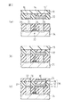
(実施例1)
図1(a)に示すように、単結晶基板10の上に、基板10の表面に平行な(111)面11を持つ単結晶PZT層12をエピタキシャル成長させる。単結晶基板10としては、例えば、MgO(111)面、SrTiO3(111)面、あるいはα−Al2O3(0001)面の基板を用いことができる。
【0029】
単結晶PZT(111)のエピタキシャル成長は、有機金属化学気相成長(MOCVD)法、分子線エピタキシー(MBE)法、あるいはパルスレーザーデポジション(PLD)法で行うことができる。成膜法はこれらに限定されるものではない。また、PZT(PbZrxTi1−xO3)に限定されず、PLZT(PbyLa1−yZrxTi1−xO3)、PLCSZT((Pb,La,Ca,Sr)(Zr,Ti)O3)などの強誘電体材料の使用が可能であり、またこれらにNbを添加した材料の使用も可能である。
【0030】
例えばMOCVD法でのPZTの成膜は、Pb(THD)2、Zr(THD)4、及びTi(i−PrO)2(THD)2を原料として使用し、基板温度550〜600℃、圧力130〜670Pa(1〜5Torr)で行うことができる。(原料化合物の式におけるTHDはトリメチルヘキサンジオネート、i−PrOはイソプロポキシを表している。)
【0031】
平坦なPZT(111)面11を有する薄膜層12を基板10全面に形成後、薄膜キャパシタとなる領域の薄膜12’を残してPZT薄膜層12をエッチングする(図1(b))。残されたPZT薄膜12’上に、PtあるいはIr材料の薄膜により下部電極14(これは後ほど別の基板と貼り合わせる際上下逆さまにされる)を形成し、そして基板10上に、後ほど貼り合わせる別の基板(半導体基板)につながる引き出し配線となる、半導体装置の回路の一部としてのプラグ16をタングステンで形成する(図1(c))。
【0032】
次に、基板10上にTEOSなどの絶縁材料の層を形成し、CMPなどの平坦化手法により表面を平坦化して絶縁膜18(図1(d))を形成する。引き続き、下部電極14とタングステンプラグ16の上にタングステン薄膜20を形成し、TEOS絶縁材料層をもう一度形成してから平坦化して、層間絶縁膜22を形成する(図1(e))。
【0033】
図2(a)に示したように、キャパシタ用の強誘電体PZT薄膜12’を形成した基板10をひっくり返し、半導体装置の回路の一部としてのトランジスタ23が予め形成してある半導体基板24と向かい合わせにする。続いて、図2(b)に示したように、基板10のタングステン薄膜20が基板22のトランジスタの引き出し電極26と接合するように、基板10と基板24を密着させ、熱処理をおこない、2つの基板を貼り合わせて機械的、電気的に結合する。ウエハ状の2枚の基板を熱処理により貼り合わせる技術は、例えば特開平2−303114号公報、特開平1−115143号公報に記載されている。
【0034】
次に、キャパシタ用の強誘電体PZT薄膜12’を形成するのに用いた基板10を除去する。基板10の除去は、基板10がMgO基板の場合、HClを用いて化学的に溶解させる。SrTiO3基板の場合は、HNO3、HF及びHClの混酸を用いて化学的に溶解させる。サファイア(α−Al2O3)基板の場合は、溶融KOHでないと溶解しないので、SiC研磨材を用いて機械的に、あるいはコロイダルシリカを用いて機械化学的に除去する。
【0035】
最後に、図2(c)に示したように、キャパシタの上部電極28とこれに接続するタングステン薄膜30、タングステンプラグ16に接続する別のタングステンプラグ32、及び層間絶縁膜34を、先に説明したのと同様に形成して、下部電極14、強誘電体PZT薄膜12’及び上部電極28から構成された強誘電体キャパシタ36を備えた半導体装置が得られる。上部電極28は、例えばIr又はIrO2で形成することができる。
【0036】
(実施例2)
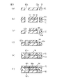
この例は、貫通孔を形成したサファイア(α−Al2O3)基板の(0001)面上にPZT薄膜を形成することによる、強誘電体キャパシタを組み入れた半導体装置の製造を説明する。
【0037】
図3(a)に示したように、(0001)面51を上面とするサファイア(α−Al2O3)単結晶基板50に貫通孔52a、52bをあける。貫通孔52aは、キャパシタの一方の電極に接続するプラグの形成用であり、貫通孔52bは、後に貼り合わせる半導体基板(回路基板)につながる引き出し配線となるプラグの形成用である。これらの貫通孔は、サファイア基板50を機械的に加工して形成してもよいし、あるいは反応性ガスを用いたドライエッチング法又はArイオンを用いたイオンミリング法で形成してもよく、あるいは溶融KOHを用いて化学的にエッチングして形成してもよい。
【0038】
図3(b)に示したように、基板50の(0001)面51に、この面51に平行な(111)面55を有する薄膜54を形成する。この薄膜54は強誘電体キャパシタの一方の電極となる薄膜であり、PtあるいはIrで形成することができる。更に、薄膜54の上に、やはり基板50の(0001)面51に平行な(111)面57を有するPZT薄膜56を形成する。Pt(111)面あるいはIr(111)面の上に成長したPZT薄膜は、PtあるいはIr結晶と格子定数が合わないため、完全な単結晶とはならないが、配向性の強い多結晶薄膜((111)面に配向した多結晶薄膜)となる。PtあるいはIr薄膜に代えてSrRuO3薄膜を使用すれば、単結晶PZT薄膜を得ることができる。次いで、図3(c)に示したように、キャパシタの強誘電体薄膜58となる部分と電極60となる部分を残して、薄膜56、54(図3(b))を除去する。
【0039】
図3(d)に示したように、貫通孔52a、52b(図3(c))内にタングステンを充填し、貫通孔52a内のタングステンには電極60に接続するプラグ62aを形成させる。貫通孔52b内のタングステンの上には更にタングステンを柱状に伸ばし、後に貼り合わせる半導体基板につながる引き出し配線となるプラグ62bを形成する。
【0040】
基板50上にTEOSなどの絶縁材料の層を形成し、表面を平坦化して絶縁膜64(図3(e))を形成する。次いで、図3(f)に示したように、強誘電体薄膜58の上に、基板50の面に平行な(111)面を持つPt又はIr薄膜のもう一方の電極66を形成し、この電極66及びタングステンプラグ62bの上にタングステン薄膜68a及び68bをそれぞれ形成し、TEOS絶縁材料層をもう一度形成してから平坦化して、層間絶縁膜70を形成する(図3(f))。
【0041】
この例では、上記のとおり強誘電体薄膜58とこれを挟む二つの電極60、66から構成されるキャパシタを形成した基板50をひっくり返すか、あるいはひっくり返さずに、予めトランジスタを形成した別の基板と貼り合わせることができる。基板50をひっくり返す場合は、図4に示したように、キャパシタの電極66が下部電極として、タングステン薄膜68aを介し、もう一方の基板(半導体基板)74に形成したトランジスタ76の一方の引き出し電極78aに接続し、タングステンプラグ62bがタングステン薄膜68bを介してもう一方の引き出し電極78bに接続する。基板50をひっくり返さない場合は、図5に示したように、キャパシタの電極60が下部電極として、タングステンプラグ62aを介しもう一方の基板74のトランジスタ76の一方の引き出し電極78aに接続し、タングステンプラグ62bがもう一方の引き出し電極78bに接続する。
【0042】
(実施例3)
この例は、貫通孔を形成したシリコン基板の(111)面上にPZT薄膜を形成することによる、強誘電体キャパシタを組み入れた半導体装置の製造を説明する。
【0043】
図6(a)に示したように、(111)面91を上面とするシリコン基板90に貫通孔92a、92bをあける。貫通孔92aは、キャパシタの一方の電極に接続するプラグの形成用であり、貫通孔92bは、後に貼り合わせる半導体基板につながる引き出し配線となるプラグの形成用である。これらの貫通孔は、シリコン基板90を機械的に加工して形成してもよいし、あるいは反応性ガスを用いたドライエッチング法又はArイオンを用いたイオンミリング法で形成してもよく、あるいはHFとHNO3の混酸を用いて化学的にエッチングして形成してもよい。
【0044】
図6(b)に示したように、基板90の(111)面91に、この面91に平行な(111)面95を有するMgAl2O4薄膜94を形成する。この薄膜94は、基板90の(111)面91に平行な(111)面を備えたPZT薄膜をその上に形成するためのバッファ層となり、PZT薄膜形成時のシリサイドの生成を防止する働きを持つ。続いて、薄膜94の上に強誘電体キャパシタの一方の電極となる薄膜96を、PtあるいはIrで形成する。この薄膜96も、基板90の(111)面91に平行な(111)面97を持つ。更に、薄膜96の上に、やはり基板90の(111)面91に平行な(111)面99を有するPZT薄膜98を形成する。
【0045】
次に、図6(c)に示したように、キャパシタの強誘電体薄膜100となる部分と電極102となる部分を残して、薄膜98、96(図6(b))を除去する。
【0046】
続いて、図6(d)に示したように、貫通孔92a、92b(図6(c))内にタングステンを充填し、貫通孔92a内のタングステンには電極102に接続するプラグ104aを形成させる。貫通孔92b内のタングステンの上には更にタングステンを柱状に伸ばし、後に貼り合わせる半導体基板につながる引き出し配線となるプラグ104bを形成する。
【0047】
基板90上にTEOSなどの絶縁材料の層を形成し、表面を平坦化して絶縁膜106(図6(e))を形成する。次いで、図6(f)に示したように、強誘電体薄膜100の上に、基板90の面に平行な(111)面を持つPt又はIr薄膜のもう一方の電極108を形成し、この電極108及びタングステンプラグ104bの上にタングステン薄膜110a及び110bをそれぞれ形成し、TEOS絶縁材料層をもう一度形成してから平坦化して、層間絶縁膜112を形成する(図6(f))。
【0048】
この例においても、実施例2で説明したように、強誘電体薄膜100とこれを挟む二つの電極102、108から構成されるキャパシタを形成した基板90をひっくり返すか、あるいはひっくり返さずに、予めトランジスタを形成した別の基板と貼り合わせることができる。
【0049】
(実施例4)
ここでは、貫通孔を形成したシリコン基板の(001)面上に、その面に対し平行な(111)面を持つPZT薄膜を形成することによる、強誘電体キャパシタを組み入れた半導体装置の製造を説明する。
【0050】
実施例3で説明したのと同様に、(001)面を上面とするシリコン基板に、キャパシタの一方の電極に接続するプラグの形成用の貫通孔と、後に貼り合わせる半導体基板につながる引き出し配線となるプラグ形成用の貫通孔をあける。
【0051】
一般に、シリコン基板の表面には薄い酸化膜(自然酸化膜)が存在しており、ここではシリコン基板の酸化膜が残っている(001)面に、MgAl2O4薄膜を形成する。薄い酸化膜の存在するSi(001)面に成膜されたMgAl2O4薄膜は、(111)面を有する薄膜となり、これは実施例3で言及したようにシリコン基板の表面(薄膜形成面)に平行な(111)面を備えたPZT薄膜をその上に形成するためのバッファ層となり、PZT薄膜形成時のシリサイドの生成を防止することができる。
【0052】
続いて、実施例3で先に説明した手順に従ってシリコン基板上にキャパシタを形成し、この基板と予めトランジスタを形成した別の基板とを貼り合わせることにより、強誘電体PZTキャパシタを組み込んだ半導体装置を製造することができる。
【0053】
本発明は、以上説明したとおりであるが、その特徴を種々の態様ととも付記すれば、次のとおりである。
(付記1) 強誘電体薄膜を含むキャパシタ構造を含む半導体装置を製造する方法であって、(111)面の強誘電体単結晶薄膜層の成長に適した表面を持つ単結晶基板の上に、基板面に対し平行な(111)面を持つ、Pbを含む強誘電体単結晶薄膜、又は基板面に対し平行な(111)面に配向した、Pbを含む強誘電体多結晶薄膜と、半導体装置の回路の一部とを形成して、Pbを含む強誘電体薄膜と半導体装置の回路の一部とを有する単結晶基板を作製すること、そしてこの単結晶基板を、前もって半導体装置の他の回路を形成したもう一つの基板と貼り合わせることにより両者の回路を結合し、強誘電体薄膜を含むキャパシタ構造を含む半導体装置を得ることを特徴とする半導体装置の製造方法。
(付記2) (1)単結晶基板上に、基板面に対し平行な(111)面を持つ、Pbを含む強誘電体単結晶薄膜層を形成し、該薄膜層をパターニングすることにより単結晶基板上に所定の形状をなす孤立した強誘電体薄膜を形成すること、該強誘電体薄膜上に位置し且つ所定の形状をなす、キャパシタの一方の電極を形成すること、及び単結晶基板上に半導体装置の回路の一部を形成することにより、Pbを含む強誘電体薄膜、一方の電極及び半導体装置の回路の一部を上に有する単結晶基板を作製すること、
(2)半導体装置の他の回路を形成した半導体基板を作製すること、
(3)上記単結晶基板と上記半導体基板とを貼り合わせ、両方の基板の回路を結合すること、
(4)上記単結晶基板を除去して強誘電体薄膜を露出させ、露出した強誘電体薄膜上にキャパシタのもう一方の電極を形成すること、
を含む、付記1記載の半導体装置の製造方法。
(付記3) (1)貫通孔を有する単結晶基板上に導電性薄膜層を形成すること、該導電性薄膜層上に、基板面に対し平行な(111)面を持つ、Pbを含む強誘電体単結晶薄膜、又は基板面に対し平行な(111)面に配向した、Pbを含む強誘電体多結晶薄膜層を形成すること、上記導電性薄膜層及び上記強誘電体薄膜層をパターニングすることにより、所定の形状をなす孤立した強誘電体薄膜と、所定形状をなす、キャパシタの一方の電極とを形成すること、上記強誘電体薄膜の上にキャパシタのもう一方の電極を形成すること、及び半導体装置の回路の一部を、上記単結晶基板の貫通孔を通り抜けさせて形成することにより、Pbを含む強誘電体薄膜とこれを挟む一対の電極から構成されるキャパシタ構造及び半導体装置の回路の一部を含む単結晶基板を作製すること、
(2)半導体装置の他の回路を形成した半導体基板を作製すること、
(3)上記単結晶基板と上記半導体基板とを貼り合わせ、両方の基板の回路を結合すること、
を含む、付記1記載の半導体装置の製造方法。
(付記4) 前記強誘電体が、PZT(PbZrxTi1−xO3)、PLZT(PbyLa1−yZrxTi1−xO3)、PLCSZT((Pb,La,Ca,Sr)(Zr,Ti)O3)、又はこれらにNbを添加した物質である、付記1から3までのいずれか一つに記載の半導体装置の製造方法。
(付記5) 前記単結晶基板として、強誘電体薄膜の形成面が(111)面の単結晶基板、又は(111)面からオフセット角度を有する単結晶基板を使用する、付記1から4までのいずれか一つに記載の半導体装置の製造方法。
(付記6) 前記単結晶基板がMgO又はSrTiO3単結晶基板である、付記5記載の半導体装置の製造方法。
(付記7) 前記単結晶基板として、強誘電体薄膜の形成面が(0001)面のα−Al2O3単結晶基板、又は(0001)面からオフセット角度を有するα−Al2O3単結晶基板を使用する、付記1から4までのいずれか一つに記載の半導体装置の製造方法。
(付記8) 前記単結晶基板として、強誘電体薄膜形成面が(001)面のMgAl2O4単結晶基板を使用する、付記1から4までのいずれか一つに記載の半導体装置の製造方法。
(付記9) 前記強誘電体多結晶薄膜層の形成前に、前記単結晶基板上にキャパシタの一方の電極となる導電性薄膜を形成することを更に含む、付記1から8までのいずれか一つに記載の半導体装置の製造方法。
(付記10) 前記導電性薄膜を、Pt、Ir、Ti、Ru又はそれらの酸化物から形成する、付記9記載の半導体装置の製造方法。
(付記11) 前記単結晶基板として、強誘電体薄膜の形成面が{111}面のシリコン単結晶基板、あるいは{111}面からオフセット角度を有するシリコン単結晶基板を使用する、付記1から4までのいずれか一つに記載の半導体装置の製造方法。
(付記12) 前記単結晶基板として、強誘電体薄膜の形成面が{100}面のシリコン単結晶基板、あるいは{100}面からオフセット角度を有するシリコン単結晶基板を使用する、付記1から4までのいずれか一つに記載の半導体装置の製造方法。
(付記13) 前記強誘電体薄膜を、前記単結晶基板の強誘電体薄膜形成面上に直接エピタキシャル成長させる、付記11又は12記載の半導体装置の製造方法。
(付記14) 前記強誘電体薄膜を、前記単結晶基板の強誘電体薄膜形成面の上に形成したバッファ層を介してエピタキシャル成長させる、付記11又は12記載の半導体装置の製造方法。
(付記15) 前記バッファ層を、MgO、イットリウム安定化ジルコニア、MgAl2O4、CaO、SrTiO3又はCeO2により形成し、その(111)面又は(0001)面の上に前記強誘電体薄膜を成長させる、付記14記載の半導体装置の製造方法。
(付記16) 前記強誘電体多結晶薄膜層の形成前に、前記単結晶基板上に導電性薄膜を形成する、付記13記載の半導体装置の製造方法。
(付記17) 前記導電性薄膜を、Pt、Ir、Ti、Ru又はそれらの酸化物から形成し、その(111)面の上に前記強誘電体多結晶薄膜を成長させる、付記16記載の半導体装置の製造方法。
(付記18) 前記導電性薄膜を、Pt、Ir、Ti、Ru又はそれらの酸化物で形成した層を複数積層して形成する、付記17記載の半導体装置の製造方法。
(付記19) 前記導電性薄膜を、SrRuO3、YBCO、又はLSCOにより形成し、その(111)面の上に前記強誘電体薄膜を成長させる、付記16記載の半導体装置の製造方法。
(付記20) 前記強誘電体多結晶薄膜層の形成前に、前記バッファ層上に導電性薄膜を形成する、付記14又は15記載の半導体装置の製造方法。
(付記21) 前記導電性薄膜を、Pt、Ir、Ti、Ru又はそれらの酸化物から形成し、その(111)面の上に前記強誘電体多結晶薄膜を成長させる、付記20記載の半導体装置の製造方法。
(付記22) 前記導電性薄膜を、Pt、Ir、Ti、Ru又はそれらの酸化物で形成した層を複数積層して形成する、付記21記載の半導体装置の製造方法。
(付記23) 前記導電性薄膜を、SrRuO3、YBCO、又はLSCOにより形成し、その(111)面の上に前記強誘電体薄膜を成長させる、付記20記載の半導体装置の製造方法。
【0054】
【発明の効果】
本発明の半導体装置では、キャパシタのための強誘電体薄膜として、分極軸と35.3°の角度を持つ<111>軸に垂直な面である(111)面を表面に持つ単結晶を用い、この単結晶強誘電体薄膜の分極電荷量は63μC/cm2と換算されるため、従来の配向性多結晶薄膜の30μC/cm2に比べ2倍以上の値が得られる。このように残留分極量が大きいため、本発明を利用して得られた半導体装置を不揮発性メモリとして組み込んだシステムLSIの信頼性はきわめて高くなる。
【0055】
また、本発明により得られた半導体装置においては単位面積あたりの分極電荷量が大きくなるので、キャパシタ面積を小さくしても必要な分極電荷量が確保できる。このことから、スケーリング則に沿って微細加工を行うことができるようになり、集積度の高い半導体装置の製造が可能になって、高性能化に加え低価格化を実現することができる。
【図面の簡単な説明】
【図1】実施例1の半導体装置の製造方法の前半の工程を説明する図である。
【図2】実施例1の半導体装置の製造方法の後半の工程を説明する図である。
【図3】実施例2の半導体装置の製造で用いるキャパシタを形成した単結晶基板の作製を説明する図である。
【図4】実施例2においてキャパシタを形成した単結晶基板をひっくり返して半導体回路を形成したシリコン基板に貼り合わせることにより製造した半導体装置を示す図である。
【図5】実施例2においてキャパシタを形成した単結晶基板をひっくり返さずに半導体回路を形成したシリコン基板に貼り合わせることにより製造した半導体装置を示す図である。
【図6】実施例3の半導体装置の製造で用いるキャパシタを形成した単結晶基板の作製を説明する図である。
【符号の説明】
10…単結晶基板
11…PZT(111)面
12…単結晶PZT層
12’…単結晶PZT薄膜
14…下部電極
16…タングステンプラグ
22…層間絶縁膜
23、76…トランジスタ
24、74…半導体基板
26…引き出し電極
28…上部電極
34…層間絶縁膜
36…強誘電体キャパシタ
50…サファイア基板
52a、52b、92a、92b…貫通孔
58…PZT強誘電体薄膜
60、66…電極
62a、62b…タングステンプラグ
64…絶縁膜
70…層間絶縁膜
90…シリコン基板
94…バッファ層
100…強誘電体薄膜
102、108…電極
112…層間絶縁膜[0001]
TECHNICAL FIELD OF THE INVENTION
The present invention relates to a semiconductor device, and more particularly, to a method for manufacturing a semiconductor device including a capacitor structure including a ferroelectric thin film.
[0002]
[Prior art]
2. Description of the Related Art A semiconductor device, particularly a semiconductor memory, has various characteristics. Among them, a device that retains data even when the power is turned off is called a non-volatile memory (nonvolatile memory). Among the non-volatile memories, those using a ferroelectric as a material for a capacitor for retaining electric charges are called a ferroelectric random access memory (FRAM (registered trademark)).
[0003]
The FRAM uses two remanent polarization characteristics of the ferroelectric thin film having different polarities, and retains data even when the power is turned off. The number of rewrites, which is a measure of non-volatility, is 1 × 10 10 ~ 1 × 10 12 Many times. The rewriting speed is on the order of several tens of ns, and has a high speed.
[0004]
In an FRAM, a ferroelectric which is a dielectric material for a capacitor can be polarized in one of two directions. By distinguishing the polarization directions, it becomes possible to store information of “1” corresponding to one polarization direction and “0” corresponding to the opposite polarization direction. If the dielectric material in the capacitor is not ferroelectric, that is, a paraelectric, polarization is maintained only when there is a potential difference from the electrodes, and not when the potential difference is removed. Thus, this results in a volatile operation. The direction of polarization of the ferroelectric in the FRAM can be sensed by applying a potential sufficient to switch the polarization of the capacitor.
[0005]
Ferroelectric materials used in the FRAM are a lead-based ferroelectric and a bismuth-based ferroelectric. A typical lead-based ferroelectric material is PZT (PbZr x Ti 1-x O 3 ), PLZT (Pb y La 1-y Zr x Ti 1-x O 3 ). A typical bismuth-based ferroelectric material is SBT (SrBi 2 Ta 2 O 9 ).
[0006]
As for the ferroelectric material used in the FRAM, Japanese Patent Application Laid-Open No. 13-102543 describes that a single crystal ferroelectric thin film is used as a ferroelectric material for a capacitor in the FRAM. However, this publication does not describe a method for manufacturing a semiconductor device using a single crystal ferroelectric thin film obtained by growing a single crystal substrate on a single crystal substrate as in the present invention.
[0007]
Japanese Patent Application Laid-Open No. H11-103024 discloses that a ferroelectric thin film (oriented polycrystalline thin film) in which a plurality of crystal grains are arranged in a layered structure is such that a crystal constituting a surface in contact with the thin film is oriented to a (111) plane. A semiconductor device having a structure provided on the lower electrode described above is described.
[0008]
On the other hand, Foster et al., Journal of Applied Physics, 81, 324 (1997) include (001) SrTiO. 3 (001) SrRuO as lower electrode on top 3 It is reported that a PZT (001) plane thin film is formed by MOCVD after forming a PZT thin film having a large residual polarization charge (2Pr).
[0009]
[Patent Document 1]
JP-A-13-102543
[Patent Document 2]
JP-A-11-103024
[Non-patent document 1]
Foster et al., Journal of Applied Physs.
ics, 81, 324 (1997)
[0010]
[Problems to be solved by the invention]
The system LSI using the ferroelectric material as described above for the capacitor material is used for devices handling money information and personal information such as an IC card and a smart card, and therefore needs to have extremely high reliability. In order to achieve the service life of 10 years assumed in these system LSIs, it is desired that the amount of polarization charge of the ferroelectric capacitor be as large as possible. However, a ferroelectric capacitor produced by a conventional sputtering method has a polarization charge amount of 20 to 25 μC / cm. 2 And the polarization charge amount required for actual products is 30 μC / cm. 2 It was difficult to obtain a ferroelectric capacitor satisfying the above in a high yield. 35 μC / cm polarization charge required for improving product reliability 2 It was even more difficult to obtain the above ferroelectric capacitor.
[0011]
An object of the present invention is to provide a method for manufacturing a highly reliable semiconductor device incorporating a capacitor structure including a ferroelectric thin film having a large polarization charge.
[0012]
[Means for Solving the Problems]
In the method of manufacturing a semiconductor device according to the present invention, a single crystal thin film material having a (111) plane or a polycrystalline thin film material oriented in a (111) plane is used as a ferroelectric crystal material, and electrodes are formed on both surfaces thereof. A semiconductor device including a capacitor having a larger amount of remanent polarization than a capacitor using a conventional oriented polycrystalline thin film is manufactured.
[0013]
Specifically, the method for manufacturing a semiconductor device of the present invention is a method for manufacturing a semiconductor device including a capacitor structure including a ferroelectric thin film, and is used for growing a (111) plane ferroelectric single crystal thin film layer. A ferroelectric single crystal thin film containing Pb having a (111) plane parallel to the substrate surface, or a (111) plane parallel to the substrate surface, on a single crystal substrate having a suitable surface; Forming a ferroelectric polycrystalline thin film containing Pb and a part of a circuit of a semiconductor device to form a single crystal substrate having the ferroelectric thin film containing Pb and a part of a circuit of the semiconductor device; Then, this single crystal substrate is bonded to another substrate on which another circuit of the semiconductor device is formed in advance, and the two circuits are joined to obtain a semiconductor device including a capacitor structure including a ferroelectric thin film. Features.
[0014]
In one embodiment, a method for manufacturing a semiconductor device according to the present invention includes:
(1) A ferroelectric single crystal thin film layer containing Pb having a (111) plane parallel to the substrate surface is formed on a single crystal substrate, and the thin film layer is patterned to a predetermined thickness on the single crystal substrate. Forming an isolated ferroelectric thin film having a shape of: forming one electrode of a capacitor located on the ferroelectric thin film and having a predetermined shape; and forming a semiconductor device on a single crystal substrate. Forming a part of a circuit to form a ferroelectric thin film containing Pb, one electrode, and a single crystal substrate having a part of the circuit of the semiconductor device thereon;
(2) manufacturing a semiconductor substrate on which another circuit of the semiconductor device is formed;
(3) laminating the single crystal substrate and the semiconductor substrate and coupling circuits of both substrates;
(4) removing the single crystal substrate to expose the ferroelectric thin film, and forming the other electrode of the capacitor on the exposed ferroelectric thin film;
And a method for manufacturing a semiconductor device including a capacitor structure including a ferroelectric thin film.
[0015]
In another embodiment, a method for manufacturing a semiconductor device according to the present invention includes:
(1) Forming a conductive thin film layer on a single crystal substrate having a through hole, and forming a Pb-containing ferroelectric single crystal having a (111) plane parallel to the substrate surface on the conductive thin film layer By forming a thin film or a ferroelectric polycrystalline thin film layer containing Pb oriented in a (111) plane parallel to the substrate surface, and patterning the conductive thin film layer and the ferroelectric thin film layer, Forming an isolated ferroelectric thin film having a predetermined shape and one electrode of a capacitor having a predetermined shape; forming another electrode of the capacitor on the ferroelectric thin film; and By forming a part of the circuit of the device through the through hole of the single crystal substrate, a capacitor structure including a ferroelectric thin film containing Pb and a pair of electrodes sandwiching the ferroelectric thin film and a circuit of the semiconductor device are formed. Simple connection including part To produce a substrate,
(2) manufacturing a semiconductor substrate on which another circuit of the semiconductor device is formed;
(3) laminating the single crystal substrate and the semiconductor substrate and coupling circuits of both substrates;
And a method for manufacturing a semiconductor device including a capacitor structure including a ferroelectric thin film.
[0016]
In the method of the present invention, a dielectric thin film of a capacitor is formed from a ferroelectric material containing lead (Pb). Pb-containing ferroelectric materials include PZT (PbZr x Ti 1-x O 3 ), PLZT (Pb y La 1-y Zr x Ti 1-x O 3 ), PLCSZT ((Pb, La, Ca, Sr) (Zr, Ti) O 3 ) Or a substance obtained by adding Nb thereto.
[0017]
As the single crystal substrate on which the ferroelectric thin film is formed, a single crystal substrate on which the ferroelectric thin film is formed has a (111) plane or a single crystal substrate having an offset angle from the (111) plane can be used. In general, the use of a single crystal substrate having an offset angle increases the flatness of the grown crystal surface. As a typical example of the (111) plane single crystal substrate, MgO or SrTiO 3 A single crystal substrate can be used.
[0018]
Alternatively, as a single-crystal substrate on which a ferroelectric thin film is formed, α-Al having a (0001) plane (C plane) as a formation surface 2 O 3 Α-Al having an offset angle from a single crystal substrate or (0001) plane 2 O 3 A single crystal substrate may be used. The ferroelectric thin film forming surface has a (001) plane of MgAl. 2 O 4 (Magnesia spinel) A single crystal substrate may be used.
[0019]
The above ferroelectric thin film forming substrate (MgO, SrTiO) 3 , Α-Al 2 O 3 And MgAl 2 O 4 When a single-crystal substrate) is used, a conductive thin film serving as one electrode of a capacitor may be formed on the substrate before forming the ferroelectric polycrystalline thin film layer. This conductive thin film can be formed from Pt, Ir, Ti, Ru or an oxide thereof, and its (111) plane can be used as a ferroelectric thin film formation surface.
[0020]
Alternatively, as the single crystal substrate on which the ferroelectric thin film is formed, the surface on which the ferroelectric thin film is formed is a (111) plane or a plane equivalent thereto, ie, a {111} silicon single crystal substrate, or a {111} plane. Alternatively, a silicon single crystal substrate having an offset angle from may be used. Alternatively, a silicon single crystal substrate having a {100} plane where the ferroelectric thin film is formed or a silicon single crystal substrate having an offset angle from the {100} plane may be used.
[0021]
When such a silicon single crystal substrate is used, the ferroelectric thin film can be epitaxially grown directly on the ferroelectric thin film forming surface of the substrate or via a buffer layer formed thereon. The use of the buffer layer is effective for preventing generation of silicide at the time of forming the ferroelectric thin film. The buffer layer is made of MgO, YSZ (yttrium-stabilized zirconia (ZrO 2 )), MgAl 2 O 4 , CaO, SrTiO 3 , CeO 2 The (111) plane or the (0001) plane can be used as a ferroelectric thin film formation surface.
[0022]
When using a silicon single crystal substrate and forming a ferroelectric thin film directly on the ferroelectric thin film forming surface or via a buffer layer, the substrate or the buffer layer is formed before forming the ferroelectric polycrystalline thin film layer. A conductive thin film serving as one electrode of a capacitor may be formed thereon. This conductive thin film can be formed from Pt, Ir, Ti, Ru or an oxide thereof, and its (111) plane can be used as a ferroelectric thin film formation surface. Alloys of these metal elements can also be used. Further, a plurality of layers formed from the above metals or alloys thereof may be stacked. Alternatively, the conductive thin film is SrRuO 3 , YBCO, or LSCO, and the (111) plane may be used as a ferroelectric thin film forming surface.
[0023]
BEST MODE FOR CARRYING OUT THE INVENTION
In the present invention, a ferroelectric single crystal thin film layer containing Pb having a (111) plane parallel to the substrate surface is formed on a single crystal substrate. Foster et al. In the Journal of Applied Physics, 81, 23 (1997) describe (001) SrTiO. 3 (001) SrRuO as lower electrode on top 3 Is formed, a PZT (001) plane thin film is formed by a metalorganic chemical vapor deposition (MOCVD) method, and the residual polarization charge (2Pr) of this thin film is 110 μC / cm. 2 Report that a large value was obtained. When this residual polarization charge is converted to the (111) plane, it is 63 μC / cm. 2 Which is 30 μC / cm required for the above-mentioned practical product. 2 It is shown that a value that is twice or more as compared with is obtained.
[0024]
For example, when a PZT material is used as the ferroelectric material, when the crystal type is cubic, a polarization axis exists in the (001) direction. When the (111) plane of the ferroelectric thin film single crystal is formed on the electrode, the <111> axis perpendicular to the electrode plane has an angle of 35.3 ° with respect to the <001> polarization axis. The polycrystalline ferroelectric thin film has a domain structure of 30 to 100 nm, and its polarization axis direction varies, so that it shows only a small amount of polarization charge as compared with a single crystal thin film.
[0025]
Therefore, a ferroelectric single-crystal thin-film layer having a (111) plane parallel to the substrate surface is formed on the single-crystal substrate, and the thin-film layer is etched to isolate a predetermined shape of each other on the single-crystal substrate. A ferroelectric thin film is formed, electrodes are formed on both sides of the thin film, and the two circuits are bonded together by bonding to a substrate on which a semiconductor circuit has been formed. cm 2 Thus, it is possible to manufacture a highly reliable semiconductor device incorporating a capacitor including a single crystal ferroelectric thin film exhibiting twice or more the amount of polarization charge as compared with the above.
[0026]
In the semiconductor device manufactured according to the present invention, the amount of polarization charge per unit area of the ferroelectric thin film used for the capacitor increases, so that the required amount of polarization charge can be secured even if the capacitor area is reduced. Therefore, fine processing can be performed according to the scaling rule, and a semiconductor device with a high degree of integration can be manufactured, and cost reduction in addition to high performance can be realized.
[0027]
【Example】
Next, the present invention will be further described with reference to examples. However, the invention is not limited to these examples.
[0028]
(Example 1)
As shown in FIG. 1A, a single
[0029]
Epitaxial growth of single crystal PZT (111) can be performed by metal organic chemical vapor deposition (MOCVD), molecular beam epitaxy (MBE), or pulsed laser deposition (PLD). The film forming method is not limited to these. In addition, PZT (PbZr x Ti 1-x O 3 ), But not limited to PLZT (Pb y La 1-y Zr x Ti 1-x O 3 ), PLCSZT ((Pb, La, Ca, Sr) (Zr, Ti) O 3 ) Can be used, and a material obtained by adding Nb to these can be used.
[0030]
For example, PZT film formation by the MOCVD method is performed using Pb (THD). 2 , Zr (THD) 4 , And Ti (i-PrO) 2 (THD) 2 Can be used as a raw material at a substrate temperature of 550 to 600 ° C. and a pressure of 130 to 670 Pa (1 to 5 Torr). (THD in the formula of the starting compound represents trimethylhexanedionate, and i-PrO represents isopropoxy.)
[0031]
After a
[0032]
Next, a layer of an insulating material such as TEOS is formed on the
[0033]
As shown in FIG. 2A, the
[0034]
Next, the
[0035]
Finally, as shown in FIG. 2C, the
[0036]
(Example 2)
In this example, a sapphire (α-Al 2 O 3 A description will be given of the manufacture of a semiconductor device incorporating a ferroelectric capacitor by forming a PZT thin film on the (0001) plane of a substrate.
[0037]
As shown in FIG. 3A, sapphire (α-Al 2 O 3 ) Drill through
[0038]
As shown in FIG. 3B, a
[0039]
As shown in FIG. 3D, tungsten is filled in the through
[0040]
A layer of an insulating material such as TEOS is formed on the
[0041]
In this example, as described above, the
[0042]
(Example 3)
This example describes the manufacture of a semiconductor device incorporating a ferroelectric capacitor by forming a PZT thin film on a (111) plane of a silicon substrate having a through hole.
[0043]
As shown in FIG. 6A, through
[0044]
As shown in FIG. 6B, a MgAl having a (111)
[0045]
Next, as shown in FIG. 6 (c), the
[0046]
Subsequently, as shown in FIG. 6D, tungsten is filled in the through
[0047]
A layer of an insulating material such as TEOS is formed over the
[0048]
Also in this example, as described in the second embodiment, the
[0049]
(Example 4)
Here, a semiconductor device incorporating a ferroelectric capacitor is formed by forming a PZT thin film having a (111) plane parallel to the (001) plane of a silicon substrate having a through hole formed thereon. explain.
[0050]
In the same manner as described in the third embodiment, a through hole for forming a plug connected to one electrode of a capacitor, and a lead wiring connected to a semiconductor substrate to be bonded later are formed on a silicon substrate having a (001) plane as an upper surface. A through hole for forming a plug is formed.
[0051]
In general, a thin oxide film (natural oxide film) exists on the surface of a silicon substrate. In this case, MgAl is deposited on the (001) surface of the silicon substrate where the oxide film remains. 2 O 4 Form a thin film. MgAl deposited on Si (001) surface with thin oxide film 2 O 4 The thin film is a thin film having a (111) plane, which is used for forming a PZT thin film having a (111) plane parallel to the surface of the silicon substrate (thin film forming surface) as described in the third embodiment. , And the generation of silicide during the formation of the PZT thin film can be prevented.
[0052]
Subsequently, a capacitor is formed on a silicon substrate according to the procedure described in the third embodiment, and this substrate is bonded to another substrate on which a transistor has been formed in advance, thereby forming a semiconductor device incorporating a ferroelectric PZT capacitor. Can be manufactured.
[0053]
Although the present invention has been described above, the features of the present invention will be described below with various aspects thereof.
(Supplementary Note 1) A method of manufacturing a semiconductor device including a capacitor structure including a ferroelectric thin film, the method comprising: forming a ferroelectric single crystal thin film layer having a surface suitable for growing a (111) plane on a single crystal substrate; A ferroelectric single crystal thin film containing Pb having a (111) plane parallel to the substrate surface, or a ferroelectric polycrystalline thin film containing Pb oriented to the (111) plane parallel to the substrate surface; Forming a part of a circuit of the semiconductor device to form a single crystal substrate having a ferroelectric thin film containing Pb and a part of the circuit of the semiconductor device; and forming the single crystal substrate in advance of the semiconductor device. A method for manufacturing a semiconductor device, comprising bonding both circuits by bonding to another substrate on which another circuit is formed to obtain a semiconductor device including a capacitor structure including a ferroelectric thin film.
(Supplementary Note 2) (1) A ferroelectric single crystal thin film layer containing Pb having a (111) plane parallel to the substrate surface is formed on a single crystal substrate, and the single crystal is formed by patterning the thin film layer. Forming an isolated ferroelectric thin film having a predetermined shape on a substrate, forming one electrode of a capacitor located on the ferroelectric thin film and having a predetermined shape, and forming on a single crystal substrate Forming a ferroelectric thin film containing Pb, one electrode and a part of the circuit of the semiconductor device thereon by forming a part of the circuit of the semiconductor device in
(2) manufacturing a semiconductor substrate on which another circuit of the semiconductor device is formed;
(3) laminating the single crystal substrate and the semiconductor substrate and coupling circuits of both substrates;
(4) removing the single crystal substrate to expose the ferroelectric thin film, and forming the other electrode of the capacitor on the exposed ferroelectric thin film;
The method for manufacturing a semiconductor device according to
(Supplementary Note 3) (1) Forming a conductive thin film layer on a single-crystal substrate having a through hole, and forming a Pb-containing layer having a (111) plane parallel to the substrate surface on the conductive thin film layer Forming a dielectric single crystal thin film or a ferroelectric polycrystalline thin film layer containing Pb oriented in a (111) plane parallel to a substrate surface, and patterning the conductive thin film layer and the ferroelectric thin film layer Thereby forming an isolated ferroelectric thin film having a predetermined shape and one electrode of a capacitor having a predetermined shape, and forming another electrode of the capacitor on the ferroelectric thin film. And forming a part of a circuit of the semiconductor device through the through-hole of the single crystal substrate, thereby forming a capacitor structure and semiconductor comprising a ferroelectric thin film containing Pb and a pair of electrodes sandwiching the ferroelectric thin film. Part of the equipment circuit Producing a single crystal substrate containing
(2) manufacturing a semiconductor substrate on which another circuit of the semiconductor device is formed;
(3) laminating the single crystal substrate and the semiconductor substrate and coupling circuits of both substrates;
The method for manufacturing a semiconductor device according to
(Supplementary Note 4) The ferroelectric substance is PZT (PbZr). x Ti 1-x O 3 ), PLZT (Pb y La 1-y Zr x Ti 1-x O 3 ), PLCSZT ((Pb, La, Ca, Sr) (Zr, Ti)
(Supplementary Note 5) As the single crystal substrate, a single crystal substrate having a ferroelectric thin film forming surface with a (111) plane or a single crystal substrate having an offset angle from the (111) plane is used. A method for manufacturing the semiconductor device according to any one of the above.
(Supplementary Note 6) The single crystal substrate is made of MgO or SrTiO. 3 6. The method for manufacturing a semiconductor device according to Supplementary Note 5, which is a single crystal substrate.
(Supplementary Note 7) As the single crystal substrate, α-Al having a (0001) plane on which a ferroelectric thin film is formed 2 O 3 Α-Al having an offset angle from a single crystal substrate or (0001) plane 2 O 3 5. The method of manufacturing a semiconductor device according to any one of
(Supplementary Note 8) As the single crystal substrate, MgAl having a (001) plane on which a ferroelectric thin film is formed 2 O 4 5. The method of manufacturing a semiconductor device according to any one of
(Supplementary note 9) Any one of
(Supplementary note 10) The method of manufacturing a semiconductor device according to supplementary note 9, wherein the conductive thin film is formed from Pt, Ir, Ti, Ru, or an oxide thereof.
(Supplementary Note 11) As the single crystal substrate, a silicon single crystal substrate having a ferroelectric thin film formation surface with a {111} plane or a silicon single crystal substrate having an offset angle from the {111} plane is used. 13. The method for manufacturing a semiconductor device according to any one of the above.
(Supplementary Note 12) As the single crystal substrate, a silicon single crystal substrate having a {100} plane where a ferroelectric thin film is formed or a silicon single crystal substrate having an offset angle from the {100} plane is used. 13. The method for manufacturing a semiconductor device according to any one of the above.
(Supplementary Note 13) The method of manufacturing a semiconductor device according to
(Supplementary note 14) The method of manufacturing a semiconductor device according to
(Supplementary Note 15) The buffer layer may be made of MgO, yttrium-stabilized zirconia, MgAl 2 O 4 , CaO, SrTiO 3 Or CeO 2 15. The method for manufacturing a semiconductor device according to
(Supplementary note 16) The method for manufacturing a semiconductor device according to supplementary note 13, wherein a conductive thin film is formed on the single crystal substrate before the formation of the ferroelectric polycrystalline thin film layer.
(Supplementary Note 17) The semiconductor according to
(Supplementary note 18) The method for manufacturing a semiconductor device according to supplementary note 17, wherein the conductive thin film is formed by stacking a plurality of layers formed of Pt, Ir, Ti, Ru, or an oxide thereof.
(Supplementary Note 19) The conductive thin film is made of SrRuO 3 17. The method of manufacturing a semiconductor device according to
(Supplementary Note 20) The method for manufacturing a semiconductor device according to
(Supplementary note 21) The semiconductor according to
(Supplementary note 22) The method of manufacturing a semiconductor device according to supplementary note 21, wherein the conductive thin film is formed by stacking a plurality of layers formed of Pt, Ir, Ti, Ru, or an oxide thereof.
(Supplementary Note 23) The conductive thin film is made of SrRuO 3 21. The method of manufacturing a semiconductor device according to
[0054]
【The invention's effect】
In the semiconductor device of the present invention, as a ferroelectric thin film for a capacitor, a single crystal having a (111) plane which is a plane perpendicular to a <111> axis having an angle of 35.3 ° with respect to a polarization axis is used. The polarization charge of this single crystal ferroelectric thin film is 63 μC / cm. 2 30 μC / cm of the conventional oriented polycrystalline thin film 2 The value obtained is twice or more as compared with. Because of such a large amount of remanent polarization, the reliability of a system LSI incorporating a semiconductor device obtained by using the present invention as a nonvolatile memory becomes extremely high.
[0055]
Further, in the semiconductor device obtained according to the present invention, the amount of polarization charge per unit area increases, so that the required amount of polarization charge can be secured even if the capacitor area is reduced. Accordingly, fine processing can be performed in accordance with the scaling rule, and a semiconductor device with a high degree of integration can be manufactured. As a result, cost reduction as well as high performance can be realized.
[Brief description of the drawings]
FIG. 1 is a diagram illustrating the first half of a method of manufacturing a semiconductor device according to a first embodiment;
FIG. 2 is a diagram illustrating the latter half of the method of manufacturing the semiconductor device according to the first embodiment.
FIG. 3 is a view for explaining the manufacture of a single crystal substrate on which a capacitor used in manufacturing the semiconductor device of Example 2 is formed.
FIG. 4 is a diagram showing a semiconductor device manufactured by turning a single crystal substrate on which a capacitor is formed in Example 2 and bonding the substrate to a silicon substrate on which a semiconductor circuit is formed;
FIG. 5 is a view showing a semiconductor device manufactured by bonding a single crystal substrate on which a capacitor is formed in Example 2 to a silicon substrate on which a semiconductor circuit is formed without turning over;
FIG. 6 is a view for explaining the manufacture of a single crystal substrate on which a capacitor used in manufacturing the semiconductor device of Example 3 is formed.
[Explanation of symbols]
10 Single crystal substrate
11 ... PZT (111) plane
12 Single crystal PZT layer
12 ': Single crystal PZT thin film
14 ... Lower electrode
16 ... Tungsten plug
22 ... interlayer insulating film
23, 76 ... transistors
24, 74: semiconductor substrate
26 ... Leader electrode
28 ... Upper electrode
34 ... Interlayer insulating film
36 ... ferroelectric capacitor
50 ... Sapphire substrate
52a, 52b, 92a, 92b ... through-hole
58 ... PZT ferroelectric thin film
60, 66 ... electrode
62a, 62b ... tungsten plug
64 ... insulating film
70 ... interlayer insulating film
90 ... Silicon substrate
94 ... buffer layer
100 ... ferroelectric thin film
102, 108 ... electrodes
112 ... interlayer insulating film
Claims (9)
(2)半導体装置の他の回路を形成した半導体基板を作製すること、
(3)上記単結晶基板と上記半導体基板とを貼り合わせ、両方の基板の回路を結合すること、
(4)上記単結晶基板を除去して強誘電体薄膜を露出させ、露出した強誘電体薄膜上にキャパシタのもう一方の電極を形成すること、
を含む、請求項1記載の半導体装置の製造方法。(1) A ferroelectric single crystal thin film layer containing Pb having a (111) plane parallel to the substrate surface is formed on a single crystal substrate, and the thin film layer is patterned to a predetermined thickness on the single crystal substrate. Forming an isolated ferroelectric thin film having a shape of: forming one electrode of a capacitor located on the ferroelectric thin film and having a predetermined shape; and forming a semiconductor device on a single crystal substrate. Forming a part of a circuit to form a ferroelectric thin film containing Pb, one electrode, and a single crystal substrate having a part of the circuit of the semiconductor device thereon;
(2) manufacturing a semiconductor substrate on which another circuit of the semiconductor device is formed;
(3) laminating the single crystal substrate and the semiconductor substrate and coupling circuits of both substrates;
(4) removing the single crystal substrate to expose the ferroelectric thin film, and forming the other electrode of the capacitor on the exposed ferroelectric thin film;
The method for manufacturing a semiconductor device according to claim 1, comprising:
(2)半導体装置の他の回路を形成した半導体基板を作製すること、
(3)上記単結晶基板と上記半導体基板とを貼り合わせ、両方の基板の回路を結合すること、
を含む、請求項1記載の半導体装置の製造方法。(1) Forming a conductive thin film layer on a single crystal substrate having a through hole, and forming a Pb-containing ferroelectric single crystal having a (111) plane parallel to the substrate surface on the conductive thin film layer By forming a thin film or a ferroelectric polycrystalline thin film layer containing Pb oriented in a (111) plane parallel to the substrate surface, and patterning the conductive thin film layer and the ferroelectric thin film layer, Forming an isolated ferroelectric thin film having a predetermined shape and one electrode of a capacitor having a predetermined shape; forming another electrode of the capacitor on the ferroelectric thin film; and By forming a part of the circuit of the device through the through hole of the single crystal substrate, a capacitor structure including a ferroelectric thin film containing Pb and a pair of electrodes sandwiching the ferroelectric thin film and a circuit of the semiconductor device are formed. Simple connection including part To produce a substrate,
(2) manufacturing a semiconductor substrate on which another circuit of the semiconductor device is formed;
(3) laminating the single crystal substrate and the semiconductor substrate and coupling circuits of both substrates;
The method for manufacturing a semiconductor device according to claim 1, comprising:
Priority Applications (5)
| Application Number | Priority Date | Filing Date | Title |
|---|---|---|---|
| JP2002328382A JP2004165351A (en) | 2002-11-12 | 2002-11-12 | Method for manufacturing semiconductor device |
| PCT/JP2003/014123 WO2004044965A2 (en) | 2002-11-12 | 2003-11-05 | Method of producing semiconductor device |
| CNB2003801030112A CN100376015C (en) | 2002-11-12 | 2003-11-05 | Method of producing semiconductor device |
| US10/532,249 US7674634B2 (en) | 2002-11-12 | 2003-11-05 | Method of producing semiconductor device |
| TW092131546A TWI228821B (en) | 2002-11-12 | 2003-11-11 | Method of producing semiconductor device |
Applications Claiming Priority (1)
| Application Number | Priority Date | Filing Date | Title |
|---|---|---|---|
| JP2002328382A JP2004165351A (en) | 2002-11-12 | 2002-11-12 | Method for manufacturing semiconductor device |
Publications (1)
| Publication Number | Publication Date |
|---|---|
| JP2004165351A true JP2004165351A (en) | 2004-06-10 |
Family
ID=32310543
Family Applications (1)
| Application Number | Title | Priority Date | Filing Date |
|---|---|---|---|
| JP2002328382A Pending JP2004165351A (en) | 2002-11-12 | 2002-11-12 | Method for manufacturing semiconductor device |
Country Status (5)
| Country | Link |
|---|---|
| US (1) | US7674634B2 (en) |
| JP (1) | JP2004165351A (en) |
| CN (1) | CN100376015C (en) |
| TW (1) | TWI228821B (en) |
| WO (1) | WO2004044965A2 (en) |
Cited By (2)
| Publication number | Priority date | Publication date | Assignee | Title |
|---|---|---|---|---|
| WO2006095425A1 (en) * | 2005-03-10 | 2006-09-14 | Fujitsu Limited | Nonvolatile semiconductor storage and method for manufacturing same |
| JP2020533779A (en) * | 2017-09-06 | 2020-11-19 | フーダン大学Fudan University | Ferroelectric memory integrated circuit and its operation method and manufacturing method |
Families Citing this family (13)
| Publication number | Priority date | Publication date | Assignee | Title |
|---|---|---|---|---|
| FI121722B (en) * | 2006-09-18 | 2011-03-15 | Valtion Teknillinen | Disc capacitor or disc resonator arrangement |
| US11527774B2 (en) | 2011-06-29 | 2022-12-13 | Space Charge, LLC | Electrochemical energy storage devices |
| US10601074B2 (en) | 2011-06-29 | 2020-03-24 | Space Charge, LLC | Rugged, gel-free, lithium-free, high energy density solid-state electrochemical energy storage devices |
| US9853325B2 (en) | 2011-06-29 | 2017-12-26 | Space Charge, LLC | Rugged, gel-free, lithium-free, high energy density solid-state electrochemical energy storage devices |
| US11996517B2 (en) | 2011-06-29 | 2024-05-28 | Space Charge, LLC | Electrochemical energy storage devices |
| KR20130060065A (en) * | 2011-11-29 | 2013-06-07 | 에스케이하이닉스 주식회사 | Non-volatile memory device and method of fabricating the same |
| CN104538539B (en) * | 2014-12-25 | 2017-06-27 | 内蒙古科技大学 | A kind of electric card effect refrigeration composite thick film material |
| CN104637949B (en) * | 2015-01-24 | 2017-11-17 | 复旦大学 | Non-destructive read-out ferroelectric memory and preparation method thereof and operating method |
| CN104637948B (en) * | 2015-01-24 | 2017-11-17 | 复旦大学 | Non-destructive read-out ferroelectric memory and preparation method thereof and read/write operation method |
| CN106409818B (en) * | 2016-10-17 | 2019-01-22 | 北京工业大学 | A kind of method that non-destructive obtains flexible ferroelectric capacitor |
| US11121139B2 (en) * | 2017-11-16 | 2021-09-14 | International Business Machines Corporation | Hafnium oxide and zirconium oxide based ferroelectric devices with textured iridium bottom electrodes |
| EP3762989A4 (en) | 2018-03-07 | 2021-12-15 | Space Charge, LLC | Thin-film solid-state energy-storage devices |
| TWI764176B (en) * | 2020-06-16 | 2022-05-11 | 光洋應用材料科技股份有限公司 | Parts for sputtering chamber and method of making the same |
Family Cites Families (14)
| Publication number | Priority date | Publication date | Assignee | Title |
|---|---|---|---|---|
| JPS60202952A (en) * | 1984-03-28 | 1985-10-14 | Fujitsu Ltd | Manufacture of semiconductor device |
| US5070026A (en) * | 1989-06-26 | 1991-12-03 | Spire Corporation | Process of making a ferroelectric electronic component and product |
| JPH06196648A (en) | 1992-12-25 | 1994-07-15 | Fuji Xerox Co Ltd | Oriented ferroelectric thin film device |
| JP2924574B2 (en) | 1993-05-31 | 1999-07-26 | 富士ゼロックス株式会社 | Oriented ferroelectric thin film device |
| JPH08186235A (en) * | 1994-12-16 | 1996-07-16 | Texas Instr Inc <Ti> | Manufacture of semiconductor device |
| JPH08227980A (en) | 1995-02-21 | 1996-09-03 | Toshiba Corp | Semiconductor device and fabrication of the same |
| KR100219519B1 (en) * | 1997-01-10 | 1999-09-01 | 윤종용 | A semiconductor device having ferroelectric floating gate ram and fabrication method of the same |
| CN1292931A (en) * | 1998-09-22 | 2001-04-25 | 株式会社日立制作所 | Ferroelectric device and semiconductor device |
| US6333202B1 (en) * | 1999-08-26 | 2001-12-25 | International Business Machines Corporation | Flip FERAM cell and method to form same |
| JP2001102543A (en) | 1999-09-30 | 2001-04-13 | Fujitsu Ltd | Semiconductor device and manufacturing method therefor |
| JP3608459B2 (en) * | 1999-12-28 | 2005-01-12 | 株式会社村田製作所 | Thin film laminate, ferroelectric thin film element, and manufacturing method thereof |
| US6396094B1 (en) | 2000-05-12 | 2002-05-28 | Agilent Technologies, Inc. | Oriented rhombohedral composition of PbZr1-xTixO3 thin films for low voltage operation ferroelectric RAM |
| JP2002016229A (en) | 2000-06-29 | 2002-01-18 | Rikogaku Shinkokai | Ferroelectric element and method of manufacturing the same |
| US6829157B2 (en) * | 2001-12-05 | 2004-12-07 | Korea Institute Of Science And Technology | Method of controlling magnetization easy axis in ferromagnetic films using voltage, ultrahigh-density, low power, nonvolatile magnetic memory using the control method, and method of writing information on the magnetic memory |
-
2002
- 2002-11-12 JP JP2002328382A patent/JP2004165351A/en active Pending
-
2003
- 2003-11-05 CN CNB2003801030112A patent/CN100376015C/en not_active Expired - Fee Related
- 2003-11-05 US US10/532,249 patent/US7674634B2/en not_active Expired - Fee Related
- 2003-11-05 WO PCT/JP2003/014123 patent/WO2004044965A2/en active Application Filing
- 2003-11-11 TW TW092131546A patent/TWI228821B/en not_active IP Right Cessation
Cited By (5)
| Publication number | Priority date | Publication date | Assignee | Title |
|---|---|---|---|---|
| WO2006095425A1 (en) * | 2005-03-10 | 2006-09-14 | Fujitsu Limited | Nonvolatile semiconductor storage and method for manufacturing same |
| JPWO2006095425A1 (en) * | 2005-03-10 | 2008-08-14 | 富士通株式会社 | Nonvolatile semiconductor memory device and manufacturing method thereof |
| JP4818255B2 (en) * | 2005-03-10 | 2011-11-16 | 富士通株式会社 | Method for manufacturing nonvolatile semiconductor memory device |
| JP2020533779A (en) * | 2017-09-06 | 2020-11-19 | フーダン大学Fudan University | Ferroelectric memory integrated circuit and its operation method and manufacturing method |
| JP7079769B2 (en) | 2017-09-06 | 2022-06-02 | フーダン大学 | Ferroelectric memory integrated circuit and its operation method and manufacturing method |
Also Published As
| Publication number | Publication date |
|---|---|
| TWI228821B (en) | 2005-03-01 |
| US20060166378A1 (en) | 2006-07-27 |
| WO2004044965A2 (en) | 2004-05-27 |
| US7674634B2 (en) | 2010-03-09 |
| CN1711624A (en) | 2005-12-21 |
| TW200414509A (en) | 2004-08-01 |
| WO2004044965A3 (en) | 2004-11-25 |
| CN100376015C (en) | 2008-03-19 |
Similar Documents
| Publication | Publication Date | Title |
|---|---|---|
| US7446361B2 (en) | Capacitor and semiconductor device having a ferroelectric material | |
| US8497181B1 (en) | Semiconductor device and method of manufacturing the same | |
| JP4578774B2 (en) | Method for manufacturing ferroelectric capacitor | |
| EP1306889B1 (en) | Electronic device with electrode and its manufacture | |
| JP4439020B2 (en) | Semiconductor memory device and manufacturing method thereof | |
| JP2004165351A (en) | Method for manufacturing semiconductor device | |
| US6376259B1 (en) | Method for manufacturing a ferroelectric memory cell including co-annealing | |
| US20110183440A1 (en) | Semiconductor device and manufacturing method thereof, and thin film device | |
| US20070040198A1 (en) | Semiconductor device and manufacturing method thereof, and thin film device | |
| JP5211560B2 (en) | Semiconductor device manufacturing method and semiconductor device | |
| JP4823895B2 (en) | Semiconductor device and manufacturing method thereof | |
| JP3212194B2 (en) | Method for manufacturing semiconductor device | |
| JP2007173396A (en) | Ferroelectric capacitor and semiconductor device | |
| JP2006245383A (en) | Capacitor for semiconductor integrated circuit | |
| JP2003152167A (en) | Capacitor of semiconductor element and its manufacturing method | |
| KR100801200B1 (en) | Semiconductor device and manufacturing method thereof, and thin film device | |
| JP2001102543A (en) | Semiconductor device and manufacturing method therefor | |
| JP2009231345A (en) | Ferroelectric material, ferroelectric capacitor, and semiconductor memory | |
| JP2007053141A (en) | Semiconductor device and its manufacturing method | |
| JPH1197638A (en) | Semiconductor memory and manufacture of the same | |
| JPH10229169A (en) | Ferroelectric memory element, manufacture thereof and integrated circuit | |
| JP2010171456A (en) | Ferroelectric capacitor, method of manufacturing the same, and semiconductor device | |
| JP2005317741A (en) | Polycrystalline substance, polycrystalline substance device and method for manufacturing the same |
Legal Events
| Date | Code | Title | Description |
|---|---|---|---|
| A621 | Written request for application examination |
Free format text: JAPANESE INTERMEDIATE CODE: A621 Effective date: 20051007 |
|
| A131 | Notification of reasons for refusal |
Free format text: JAPANESE INTERMEDIATE CODE: A131 Effective date: 20090825 |
|
| A02 | Decision of refusal |
Free format text: JAPANESE INTERMEDIATE CODE: A02 Effective date: 20091222 |