JP2004160977A - Barrier layer for article and process of forming the barrier layer using expanding thermal plasma - Google Patents
Barrier layer for article and process of forming the barrier layer using expanding thermal plasma Download PDFInfo
- Publication number
- JP2004160977A JP2004160977A JP2003144218A JP2003144218A JP2004160977A JP 2004160977 A JP2004160977 A JP 2004160977A JP 2003144218 A JP2003144218 A JP 2003144218A JP 2003144218 A JP2003144218 A JP 2003144218A JP 2004160977 A JP2004160977 A JP 2004160977A
- Authority
- JP
- Japan
- Prior art keywords
- substrate
- barrier layer
- article
- metal
- combinations
- Prior art date
- Legal status (The legal status is an assumption and is not a legal conclusion. Google has not performed a legal analysis and makes no representation as to the accuracy of the status listed.)
- Pending
Links
- 230000004888 barrier function Effects 0.000 title claims abstract description 179
- 238000000034 method Methods 0.000 title claims abstract description 70
- 239000000758 substrate Substances 0.000 claims abstract description 147
- 238000000151 deposition Methods 0.000 claims abstract description 112
- QVGXLLKOCUKJST-UHFFFAOYSA-N atomic oxygen Chemical compound [O] QVGXLLKOCUKJST-UHFFFAOYSA-N 0.000 claims abstract description 72
- 239000001301 oxygen Substances 0.000 claims abstract description 72
- 229910052760 oxygen Inorganic materials 0.000 claims abstract description 72
- 230000005540 biological transmission Effects 0.000 claims abstract description 37
- 239000004973 liquid crystal related substance Substances 0.000 claims abstract description 17
- 239000000126 substance Substances 0.000 claims abstract 2
- 239000010410 layer Substances 0.000 claims description 278
- 229910052751 metal Inorganic materials 0.000 claims description 83
- 239000002184 metal Substances 0.000 claims description 83
- 230000008021 deposition Effects 0.000 claims description 71
- 239000000376 reactant Substances 0.000 claims description 67
- 239000002243 precursor Substances 0.000 claims description 49
- 229910052782 aluminium Inorganic materials 0.000 claims description 39
- XAGFODPZIPBFFR-UHFFFAOYSA-N aluminium Chemical compound [Al] XAGFODPZIPBFFR-UHFFFAOYSA-N 0.000 claims description 39
- XLYOFNOQVPJJNP-UHFFFAOYSA-N water Chemical compound O XLYOFNOQVPJJNP-UHFFFAOYSA-N 0.000 claims description 37
- ATJFFYVFTNAWJD-UHFFFAOYSA-N Tin Chemical compound [Sn] ATJFFYVFTNAWJD-UHFFFAOYSA-N 0.000 claims description 36
- 229910052718 tin Inorganic materials 0.000 claims description 36
- HCHKCACWOHOZIP-UHFFFAOYSA-N Zinc Chemical compound [Zn] HCHKCACWOHOZIP-UHFFFAOYSA-N 0.000 claims description 35
- 229910052725 zinc Inorganic materials 0.000 claims description 35
- 239000011701 zinc Substances 0.000 claims description 35
- 229910052710 silicon Inorganic materials 0.000 claims description 32
- 239000010703 silicon Substances 0.000 claims description 32
- 150000004767 nitrides Chemical class 0.000 claims description 31
- XUIMIQQOPSSXEZ-UHFFFAOYSA-N Silicon Chemical group [Si] XUIMIQQOPSSXEZ-UHFFFAOYSA-N 0.000 claims description 29
- 229910052738 indium Inorganic materials 0.000 claims description 28
- APFVFJFRJDLVQX-UHFFFAOYSA-N indium atom Chemical compound [In] APFVFJFRJDLVQX-UHFFFAOYSA-N 0.000 claims description 28
- QGZKDVFQNNGYKY-UHFFFAOYSA-N Ammonia Chemical compound N QGZKDVFQNNGYKY-UHFFFAOYSA-N 0.000 claims description 26
- 229910044991 metal oxide Inorganic materials 0.000 claims description 25
- 150000004706 metal oxides Chemical class 0.000 claims description 25
- 239000000463 material Substances 0.000 claims description 24
- 229910052723 transition metal Inorganic materials 0.000 claims description 23
- 150000003624 transition metals Chemical class 0.000 claims description 23
- IJGRMHOSHXDMSA-UHFFFAOYSA-N Atomic nitrogen Chemical compound N#N IJGRMHOSHXDMSA-UHFFFAOYSA-N 0.000 claims description 22
- RTAQQCXQSZGOHL-UHFFFAOYSA-N Titanium Chemical compound [Ti] RTAQQCXQSZGOHL-UHFFFAOYSA-N 0.000 claims description 19
- 229910052719 titanium Inorganic materials 0.000 claims description 19
- 239000010936 titanium Substances 0.000 claims description 19
- VYPSYNLAJGMNEJ-UHFFFAOYSA-N Silicium dioxide Chemical compound O=[Si]=O VYPSYNLAJGMNEJ-UHFFFAOYSA-N 0.000 claims description 14
- PPBRXRYQALVLMV-UHFFFAOYSA-N Styrene Chemical compound C=CC1=CC=CC=C1 PPBRXRYQALVLMV-UHFFFAOYSA-N 0.000 claims description 14
- MCMNRKCIXSYSNV-UHFFFAOYSA-N Zirconium dioxide Chemical compound O=[Zr]=O MCMNRKCIXSYSNV-UHFFFAOYSA-N 0.000 claims description 14
- 239000011521 glass Substances 0.000 claims description 14
- 229910021529 ammonia Inorganic materials 0.000 claims description 13
- 229910052793 cadmium Inorganic materials 0.000 claims description 13
- 229910010272 inorganic material Inorganic materials 0.000 claims description 13
- 239000011147 inorganic material Substances 0.000 claims description 13
- 239000012790 adhesive layer Substances 0.000 claims description 12
- -1 carbide Inorganic materials 0.000 claims description 12
- 229920000642 polymer Polymers 0.000 claims description 12
- 229910052757 nitrogen Inorganic materials 0.000 claims description 11
- 229910052581 Si3N4 Inorganic materials 0.000 claims description 10
- BASFCYQUMIYNBI-UHFFFAOYSA-N platinum Chemical compound [Pt] BASFCYQUMIYNBI-UHFFFAOYSA-N 0.000 claims description 10
- 229920000307 polymer substrate Polymers 0.000 claims description 10
- HQVNEWCFYHHQES-UHFFFAOYSA-N silicon nitride Chemical compound N12[Si]34N5[Si]62N3[Si]51N64 HQVNEWCFYHHQES-UHFFFAOYSA-N 0.000 claims description 10
- 229910001868 water Inorganic materials 0.000 claims description 9
- GYHNNYVSQQEPJS-UHFFFAOYSA-N Gallium Chemical compound [Ga] GYHNNYVSQQEPJS-UHFFFAOYSA-N 0.000 claims description 8
- BLRPTPMANUNPDV-UHFFFAOYSA-N Silane Chemical compound [SiH4] BLRPTPMANUNPDV-UHFFFAOYSA-N 0.000 claims description 8
- BDOSMKKIYDKNTQ-UHFFFAOYSA-N cadmium atom Chemical compound [Cd] BDOSMKKIYDKNTQ-UHFFFAOYSA-N 0.000 claims description 8
- 229910052733 gallium Inorganic materials 0.000 claims description 8
- 150000002894 organic compounds Chemical class 0.000 claims description 8
- 239000011368 organic material Substances 0.000 claims description 8
- 230000035699 permeability Effects 0.000 claims description 8
- 229910000077 silane Inorganic materials 0.000 claims description 8
- VXUYXOFXAQZZMF-UHFFFAOYSA-N titanium(IV) isopropoxide Chemical compound CC(C)O[Ti](OC(C)C)(OC(C)C)OC(C)C VXUYXOFXAQZZMF-UHFFFAOYSA-N 0.000 claims description 8
- NLHHRLWOUZZQLW-UHFFFAOYSA-N Acrylonitrile Chemical compound C=CC#N NLHHRLWOUZZQLW-UHFFFAOYSA-N 0.000 claims description 7
- 229910052580 B4C Inorganic materials 0.000 claims description 7
- 229910052582 BN Inorganic materials 0.000 claims description 7
- ZOXJGFHDIHLPTG-UHFFFAOYSA-N Boron Chemical compound [B] ZOXJGFHDIHLPTG-UHFFFAOYSA-N 0.000 claims description 7
- PZNSFCLAULLKQX-UHFFFAOYSA-N Boron nitride Chemical compound N#B PZNSFCLAULLKQX-UHFFFAOYSA-N 0.000 claims description 7
- VYZAMTAEIAYCRO-UHFFFAOYSA-N Chromium Chemical compound [Cr] VYZAMTAEIAYCRO-UHFFFAOYSA-N 0.000 claims description 7
- ZOKXTWBITQBERF-UHFFFAOYSA-N Molybdenum Chemical compound [Mo] ZOKXTWBITQBERF-UHFFFAOYSA-N 0.000 claims description 7
- CTQNGGLPUBDAKN-UHFFFAOYSA-N O-Xylene Chemical compound CC1=CC=CC=C1C CTQNGGLPUBDAKN-UHFFFAOYSA-N 0.000 claims description 7
- GWEVSGVZZGPLCZ-UHFFFAOYSA-N Titan oxide Chemical compound O=[Ti]=O GWEVSGVZZGPLCZ-UHFFFAOYSA-N 0.000 claims description 7
- QCWXUUIWCKQGHC-UHFFFAOYSA-N Zirconium Chemical compound [Zr] QCWXUUIWCKQGHC-UHFFFAOYSA-N 0.000 claims description 7
- PNEYBMLMFCGWSK-UHFFFAOYSA-N aluminium oxide Inorganic materials [O-2].[O-2].[O-2].[Al+3].[Al+3] PNEYBMLMFCGWSK-UHFFFAOYSA-N 0.000 claims description 7
- 229910003481 amorphous carbon Inorganic materials 0.000 claims description 7
- 229910052796 boron Inorganic materials 0.000 claims description 7
- INAHAJYZKVIDIZ-UHFFFAOYSA-N boron carbide Chemical compound B12B3B4C32B41 INAHAJYZKVIDIZ-UHFFFAOYSA-N 0.000 claims description 7
- 229910010293 ceramic material Inorganic materials 0.000 claims description 7
- 229910052804 chromium Inorganic materials 0.000 claims description 7
- 239000011651 chromium Substances 0.000 claims description 7
- 229910052732 germanium Inorganic materials 0.000 claims description 7
- GNPVGFCGXDBREM-UHFFFAOYSA-N germanium atom Chemical compound [Ge] GNPVGFCGXDBREM-UHFFFAOYSA-N 0.000 claims description 7
- 229910052735 hafnium Inorganic materials 0.000 claims description 7
- VBJZVLUMGGDVMO-UHFFFAOYSA-N hafnium atom Chemical compound [Hf] VBJZVLUMGGDVMO-UHFFFAOYSA-N 0.000 claims description 7
- 229910052750 molybdenum Inorganic materials 0.000 claims description 7
- 239000011733 molybdenum Substances 0.000 claims description 7
- 229920000515 polycarbonate Polymers 0.000 claims description 7
- 239000004417 polycarbonate Substances 0.000 claims description 7
- 239000000377 silicon dioxide Substances 0.000 claims description 7
- 229910052715 tantalum Inorganic materials 0.000 claims description 7
- GUVRBAGPIYLISA-UHFFFAOYSA-N tantalum atom Chemical compound [Ta] GUVRBAGPIYLISA-UHFFFAOYSA-N 0.000 claims description 7
- OGIDPMRJRNCKJF-UHFFFAOYSA-N titanium oxide Inorganic materials [Ti]=O OGIDPMRJRNCKJF-UHFFFAOYSA-N 0.000 claims description 7
- WFKWXMTUELFFGS-UHFFFAOYSA-N tungsten Chemical compound [W] WFKWXMTUELFFGS-UHFFFAOYSA-N 0.000 claims description 7
- 229910052721 tungsten Inorganic materials 0.000 claims description 7
- 239000010937 tungsten Substances 0.000 claims description 7
- 229910052720 vanadium Inorganic materials 0.000 claims description 7
- LEONUFNNVUYDNQ-UHFFFAOYSA-N vanadium atom Chemical compound [V] LEONUFNNVUYDNQ-UHFFFAOYSA-N 0.000 claims description 7
- 239000008096 xylene Substances 0.000 claims description 7
- 229910052726 zirconium Inorganic materials 0.000 claims description 7
- XLOMVQKBTHCTTD-UHFFFAOYSA-N Zinc monoxide Chemical compound [Zn]=O XLOMVQKBTHCTTD-UHFFFAOYSA-N 0.000 claims description 6
- KPUWHANPEXNPJT-UHFFFAOYSA-N disiloxane Chemical class [SiH3]O[SiH3] KPUWHANPEXNPJT-UHFFFAOYSA-N 0.000 claims description 6
- 239000001257 hydrogen Substances 0.000 claims description 6
- 229910052739 hydrogen Inorganic materials 0.000 claims description 6
- 150000001247 metal acetylides Chemical class 0.000 claims description 6
- 229910001507 metal halide Inorganic materials 0.000 claims description 6
- 150000005309 metal halides Chemical class 0.000 claims description 6
- 229920001296 polysiloxane Polymers 0.000 claims description 6
- 239000004695 Polyether sulfone Substances 0.000 claims description 5
- 239000004698 Polyethylene Substances 0.000 claims description 5
- 239000004642 Polyimide Substances 0.000 claims description 5
- BQCADISMDOOEFD-UHFFFAOYSA-N Silver Chemical compound [Ag] BQCADISMDOOEFD-UHFFFAOYSA-N 0.000 claims description 5
- 229910000831 Steel Inorganic materials 0.000 claims description 5
- 239000003365 glass fiber Substances 0.000 claims description 5
- AMGQUBHHOARCQH-UHFFFAOYSA-N indium;oxotin Chemical compound [In].[Sn]=O AMGQUBHHOARCQH-UHFFFAOYSA-N 0.000 claims description 5
- 239000000178 monomer Substances 0.000 claims description 5
- 229910052697 platinum Inorganic materials 0.000 claims description 5
- 229920000636 poly(norbornene) polymer Polymers 0.000 claims description 5
- 229920000058 polyacrylate Polymers 0.000 claims description 5
- 229920006393 polyether sulfone Polymers 0.000 claims description 5
- 229920000573 polyethylene Polymers 0.000 claims description 5
- 229920001721 polyimide Polymers 0.000 claims description 5
- 229910052709 silver Inorganic materials 0.000 claims description 5
- 239000004332 silver Substances 0.000 claims description 5
- 229940071182 stannate Drugs 0.000 claims description 5
- 239000010959 steel Substances 0.000 claims description 5
- 239000005046 Chlorosilane Substances 0.000 claims description 4
- KOPOQZFJUQMUML-UHFFFAOYSA-N chlorosilane Chemical compound Cl[SiH3] KOPOQZFJUQMUML-UHFFFAOYSA-N 0.000 claims description 4
- PZPGRFITIJYNEJ-UHFFFAOYSA-N disilane Chemical compound [SiH3][SiH3] PZPGRFITIJYNEJ-UHFFFAOYSA-N 0.000 claims description 4
- FZHAPNGMFPVSLP-UHFFFAOYSA-N silanamine Chemical compound [SiH3]N FZHAPNGMFPVSLP-UHFFFAOYSA-N 0.000 claims description 4
- 238000005299 abrasion Methods 0.000 claims description 3
- SMZOGRDCAXLAAR-UHFFFAOYSA-N aluminium isopropoxide Chemical compound [Al+3].CC(C)[O-].CC(C)[O-].CC(C)[O-] SMZOGRDCAXLAAR-UHFFFAOYSA-N 0.000 claims description 3
- 229910000420 cerium oxide Inorganic materials 0.000 claims description 3
- HQWPLXHWEZZGKY-UHFFFAOYSA-N diethylzinc Chemical compound CC[Zn]CC HQWPLXHWEZZGKY-UHFFFAOYSA-N 0.000 claims description 3
- AXAZMDOAUQTMOW-UHFFFAOYSA-N dimethylzinc Chemical compound C[Zn]C AXAZMDOAUQTMOW-UHFFFAOYSA-N 0.000 claims description 3
- BMMGVYCKOGBVEV-UHFFFAOYSA-N oxo(oxoceriooxy)cerium Chemical compound [Ce]=O.O=[Ce]=O BMMGVYCKOGBVEV-UHFFFAOYSA-N 0.000 claims description 3
- OVZUSPADPSOQQN-UHFFFAOYSA-N tri(propan-2-yloxy)indigane Chemical compound [In+3].CC(C)[O-].CC(C)[O-].CC(C)[O-] OVZUSPADPSOQQN-UHFFFAOYSA-N 0.000 claims description 3
- SSEICBQSWNBGQZ-UHFFFAOYSA-N tris[(2-methylpropan-2-yl)oxy]indigane Chemical compound CC(C)(C)O[In](OC(C)(C)C)OC(C)(C)C SSEICBQSWNBGQZ-UHFFFAOYSA-N 0.000 claims description 3
- 239000011787 zinc oxide Substances 0.000 claims description 3
- NIXOWILDQLNWCW-UHFFFAOYSA-M Acrylate Chemical compound [O-]C(=O)C=C NIXOWILDQLNWCW-UHFFFAOYSA-M 0.000 claims 6
- 150000002118 epoxides Chemical class 0.000 claims 6
- 229920000620 organic polymer Polymers 0.000 claims 4
- 125000004435 hydrogen atom Chemical class [H]* 0.000 claims 3
- 239000004411 aluminium Substances 0.000 claims 2
- 229910001510 metal chloride Inorganic materials 0.000 claims 2
- 150000002739 metals Chemical class 0.000 claims 2
- 229920000592 inorganic polymer Polymers 0.000 claims 1
- 230000005855 radiation Effects 0.000 abstract description 4
- 238000004026 adhesive bonding Methods 0.000 abstract 1
- 239000007789 gas Substances 0.000 description 24
- XKRFYHLGVUSROY-UHFFFAOYSA-N Argon Chemical compound [Ar] XKRFYHLGVUSROY-UHFFFAOYSA-N 0.000 description 14
- 230000005525 hole transport Effects 0.000 description 8
- 229910052786 argon Inorganic materials 0.000 description 7
- 238000000576 coating method Methods 0.000 description 7
- 238000000623 plasma-assisted chemical vapour deposition Methods 0.000 description 6
- 238000006243 chemical reaction Methods 0.000 description 5
- 238000010586 diagram Methods 0.000 description 5
- 230000007613 environmental effect Effects 0.000 description 4
- 150000001768 cations Chemical class 0.000 description 3
- 239000001307 helium Substances 0.000 description 3
- 229910052734 helium Inorganic materials 0.000 description 3
- SWQJXJOGLNCZEY-UHFFFAOYSA-N helium atom Chemical compound [He] SWQJXJOGLNCZEY-UHFFFAOYSA-N 0.000 description 3
- 229920006289 polycarbonate film Polymers 0.000 description 3
- ATUOYWHBWRKTHZ-UHFFFAOYSA-N Propane Chemical compound CCC ATUOYWHBWRKTHZ-UHFFFAOYSA-N 0.000 description 2
- 239000011248 coating agent Substances 0.000 description 2
- 239000007772 electrode material Substances 0.000 description 2
- 239000012530 fluid Substances 0.000 description 2
- 150000002431 hydrogen Chemical class 0.000 description 2
- 238000007735 ion beam assisted deposition Methods 0.000 description 2
- 150000002500 ions Chemical class 0.000 description 2
- 239000000203 mixture Substances 0.000 description 2
- 230000006798 recombination Effects 0.000 description 2
- 238000005215 recombination Methods 0.000 description 2
- 239000004065 semiconductor Substances 0.000 description 2
- 239000002356 single layer Substances 0.000 description 2
- UFHFLCQGNIYNRP-UHFFFAOYSA-N Hydrogen Chemical compound [H][H] UFHFLCQGNIYNRP-UHFFFAOYSA-N 0.000 description 1
- FYYHWMGAXLPEAU-UHFFFAOYSA-N Magnesium Chemical compound [Mg] FYYHWMGAXLPEAU-UHFFFAOYSA-N 0.000 description 1
- 241000204667 Thermoplasma Species 0.000 description 1
- 230000002411 adverse Effects 0.000 description 1
- HSFWRNGVRCDJHI-UHFFFAOYSA-N alpha-acetylene Natural products C#C HSFWRNGVRCDJHI-UHFFFAOYSA-N 0.000 description 1
- VSCWAEJMTAWNJL-UHFFFAOYSA-K aluminium trichloride Chemical class Cl[Al](Cl)Cl VSCWAEJMTAWNJL-UHFFFAOYSA-K 0.000 description 1
- 239000001273 butane Substances 0.000 description 1
- 238000005229 chemical vapour deposition Methods 0.000 description 1
- 238000001816 cooling Methods 0.000 description 1
- 238000010494 dissociation reaction Methods 0.000 description 1
- 230000005593 dissociations Effects 0.000 description 1
- 229940079593 drug Drugs 0.000 description 1
- 239000003814 drug Substances 0.000 description 1
- 230000000694 effects Effects 0.000 description 1
- 238000005538 encapsulation Methods 0.000 description 1
- 125000002534 ethynyl group Chemical group [H]C#C* 0.000 description 1
- 230000008020 evaporation Effects 0.000 description 1
- 238000001704 evaporation Methods 0.000 description 1
- 238000006062 fragmentation reaction Methods 0.000 description 1
- 238000003384 imaging method Methods 0.000 description 1
- 238000009616 inductively coupled plasma Methods 0.000 description 1
- 239000011261 inert gas Substances 0.000 description 1
- 238000002347 injection Methods 0.000 description 1
- 239000007924 injection Substances 0.000 description 1
- 229910052743 krypton Inorganic materials 0.000 description 1
- DNNSSWSSYDEUBZ-UHFFFAOYSA-N krypton atom Chemical compound [Kr] DNNSSWSSYDEUBZ-UHFFFAOYSA-N 0.000 description 1
- 229910052749 magnesium Inorganic materials 0.000 description 1
- 239000011777 magnesium Substances 0.000 description 1
- 238000012986 modification Methods 0.000 description 1
- 230000004048 modification Effects 0.000 description 1
- IJDNQMDRQITEOD-UHFFFAOYSA-N n-butane Chemical compound CCCC IJDNQMDRQITEOD-UHFFFAOYSA-N 0.000 description 1
- OFBQJSOFQDEBGM-UHFFFAOYSA-N n-pentane Natural products CCCCC OFBQJSOFQDEBGM-UHFFFAOYSA-N 0.000 description 1
- 229910052754 neon Inorganic materials 0.000 description 1
- GKAOGPIIYCISHV-UHFFFAOYSA-N neon atom Chemical compound [Ne] GKAOGPIIYCISHV-UHFFFAOYSA-N 0.000 description 1
- 229910052756 noble gas Inorganic materials 0.000 description 1
- 230000000704 physical effect Effects 0.000 description 1
- 239000002861 polymer material Substances 0.000 description 1
- 239000001294 propane Substances 0.000 description 1
- 239000011253 protective coating Substances 0.000 description 1
- 150000004756 silanes Chemical class 0.000 description 1
- LIVNPJMFVYWSIS-UHFFFAOYSA-N silicon monoxide Chemical class [Si-]#[O+] LIVNPJMFVYWSIS-UHFFFAOYSA-N 0.000 description 1
- 229910052814 silicon oxide Inorganic materials 0.000 description 1
- 238000004544 sputter deposition Methods 0.000 description 1
- 238000006467 substitution reaction Methods 0.000 description 1
- XJDNKRIXUMDJCW-UHFFFAOYSA-J titanium tetrachloride Chemical compound Cl[Ti](Cl)(Cl)Cl XJDNKRIXUMDJCW-UHFFFAOYSA-J 0.000 description 1
- 229910052724 xenon Inorganic materials 0.000 description 1
- FHNFHKCVQCLJFQ-UHFFFAOYSA-N xenon atom Chemical compound [Xe] FHNFHKCVQCLJFQ-UHFFFAOYSA-N 0.000 description 1
Images


Classifications
-
- H—ELECTRICITY
- H01—ELECTRIC ELEMENTS
- H01L—SEMICONDUCTOR DEVICES NOT COVERED BY CLASS H10
- H01L23/00—Details of semiconductor or other solid state devices
- H01L23/564—Details not otherwise provided for, e.g. protection against moisture
-
- C—CHEMISTRY; METALLURGY
- C23—COATING METALLIC MATERIAL; COATING MATERIAL WITH METALLIC MATERIAL; CHEMICAL SURFACE TREATMENT; DIFFUSION TREATMENT OF METALLIC MATERIAL; COATING BY VACUUM EVAPORATION, BY SPUTTERING, BY ION IMPLANTATION OR BY CHEMICAL VAPOUR DEPOSITION, IN GENERAL; INHIBITING CORROSION OF METALLIC MATERIAL OR INCRUSTATION IN GENERAL
- C23C—COATING METALLIC MATERIAL; COATING MATERIAL WITH METALLIC MATERIAL; SURFACE TREATMENT OF METALLIC MATERIAL BY DIFFUSION INTO THE SURFACE, BY CHEMICAL CONVERSION OR SUBSTITUTION; COATING BY VACUUM EVAPORATION, BY SPUTTERING, BY ION IMPLANTATION OR BY CHEMICAL VAPOUR DEPOSITION, IN GENERAL
- C23C16/00—Chemical coating by decomposition of gaseous compounds, without leaving reaction products of surface material in the coating, i.e. chemical vapour deposition [CVD] processes
- C23C16/22—Chemical coating by decomposition of gaseous compounds, without leaving reaction products of surface material in the coating, i.e. chemical vapour deposition [CVD] processes characterised by the deposition of inorganic material, other than metallic material
- C23C16/30—Deposition of compounds, mixtures or solid solutions, e.g. borides, carbides, nitrides
- C23C16/34—Nitrides
- C23C16/345—Silicon nitride
-
- C—CHEMISTRY; METALLURGY
- C23—COATING METALLIC MATERIAL; COATING MATERIAL WITH METALLIC MATERIAL; CHEMICAL SURFACE TREATMENT; DIFFUSION TREATMENT OF METALLIC MATERIAL; COATING BY VACUUM EVAPORATION, BY SPUTTERING, BY ION IMPLANTATION OR BY CHEMICAL VAPOUR DEPOSITION, IN GENERAL; INHIBITING CORROSION OF METALLIC MATERIAL OR INCRUSTATION IN GENERAL
- C23C—COATING METALLIC MATERIAL; COATING MATERIAL WITH METALLIC MATERIAL; SURFACE TREATMENT OF METALLIC MATERIAL BY DIFFUSION INTO THE SURFACE, BY CHEMICAL CONVERSION OR SUBSTITUTION; COATING BY VACUUM EVAPORATION, BY SPUTTERING, BY ION IMPLANTATION OR BY CHEMICAL VAPOUR DEPOSITION, IN GENERAL
- C23C16/00—Chemical coating by decomposition of gaseous compounds, without leaving reaction products of surface material in the coating, i.e. chemical vapour deposition [CVD] processes
- C23C16/44—Chemical coating by decomposition of gaseous compounds, without leaving reaction products of surface material in the coating, i.e. chemical vapour deposition [CVD] processes characterised by the method of coating
- C23C16/50—Chemical coating by decomposition of gaseous compounds, without leaving reaction products of surface material in the coating, i.e. chemical vapour deposition [CVD] processes characterised by the method of coating using electric discharges
- C23C16/513—Chemical coating by decomposition of gaseous compounds, without leaving reaction products of surface material in the coating, i.e. chemical vapour deposition [CVD] processes characterised by the method of coating using electric discharges using plasma jets
-
- H—ELECTRICITY
- H10—SEMICONDUCTOR DEVICES; ELECTRIC SOLID-STATE DEVICES NOT OTHERWISE PROVIDED FOR
- H10K—ORGANIC ELECTRIC SOLID-STATE DEVICES
- H10K50/00—Organic light-emitting devices
- H10K50/80—Constructional details
- H10K50/84—Passivation; Containers; Encapsulations
- H10K50/844—Encapsulations
-
- C—CHEMISTRY; METALLURGY
- C09—DYES; PAINTS; POLISHES; NATURAL RESINS; ADHESIVES; COMPOSITIONS NOT OTHERWISE PROVIDED FOR; APPLICATIONS OF MATERIALS NOT OTHERWISE PROVIDED FOR
- C09K—MATERIALS FOR MISCELLANEOUS APPLICATIONS, NOT PROVIDED FOR ELSEWHERE
- C09K2323/00—Functional layers of liquid crystal optical display excluding electroactive liquid crystal layer characterised by chemical composition
-
- H—ELECTRICITY
- H01—ELECTRIC ELEMENTS
- H01L—SEMICONDUCTOR DEVICES NOT COVERED BY CLASS H10
- H01L2924/00—Indexing scheme for arrangements or methods for connecting or disconnecting semiconductor or solid-state bodies as covered by H01L24/00
- H01L2924/0001—Technical content checked by a classifier
- H01L2924/0002—Not covered by any one of groups H01L24/00, H01L24/00 and H01L2224/00
-
- H—ELECTRICITY
- H01—ELECTRIC ELEMENTS
- H01L—SEMICONDUCTOR DEVICES NOT COVERED BY CLASS H10
- H01L2924/00—Indexing scheme for arrangements or methods for connecting or disconnecting semiconductor or solid-state bodies as covered by H01L24/00
- H01L2924/10—Details of semiconductor or other solid state devices to be connected
- H01L2924/11—Device type
- H01L2924/12—Passive devices, e.g. 2 terminal devices
- H01L2924/1204—Optical Diode
- H01L2924/12044—OLED
-
- Y—GENERAL TAGGING OF NEW TECHNOLOGICAL DEVELOPMENTS; GENERAL TAGGING OF CROSS-SECTIONAL TECHNOLOGIES SPANNING OVER SEVERAL SECTIONS OF THE IPC; TECHNICAL SUBJECTS COVERED BY FORMER USPC CROSS-REFERENCE ART COLLECTIONS [XRACs] AND DIGESTS
- Y02—TECHNOLOGIES OR APPLICATIONS FOR MITIGATION OR ADAPTATION AGAINST CLIMATE CHANGE
- Y02T—CLIMATE CHANGE MITIGATION TECHNOLOGIES RELATED TO TRANSPORTATION
- Y02T50/00—Aeronautics or air transport
- Y02T50/60—Efficient propulsion technologies, e.g. for aircraft
-
- Y—GENERAL TAGGING OF NEW TECHNOLOGICAL DEVELOPMENTS; GENERAL TAGGING OF CROSS-SECTIONAL TECHNOLOGIES SPANNING OVER SEVERAL SECTIONS OF THE IPC; TECHNICAL SUBJECTS COVERED BY FORMER USPC CROSS-REFERENCE ART COLLECTIONS [XRACs] AND DIGESTS
- Y10—TECHNICAL SUBJECTS COVERED BY FORMER USPC
- Y10S—TECHNICAL SUBJECTS COVERED BY FORMER USPC CROSS-REFERENCE ART COLLECTIONS [XRACs] AND DIGESTS
- Y10S428/00—Stock material or miscellaneous articles
- Y10S428/913—Material designed to be responsive to temperature, light, moisture
-
- Y—GENERAL TAGGING OF NEW TECHNOLOGICAL DEVELOPMENTS; GENERAL TAGGING OF CROSS-SECTIONAL TECHNOLOGIES SPANNING OVER SEVERAL SECTIONS OF THE IPC; TECHNICAL SUBJECTS COVERED BY FORMER USPC CROSS-REFERENCE ART COLLECTIONS [XRACs] AND DIGESTS
- Y10—TECHNICAL SUBJECTS COVERED BY FORMER USPC
- Y10T—TECHNICAL SUBJECTS COVERED BY FORMER US CLASSIFICATION
- Y10T428/00—Stock material or miscellaneous articles
- Y10T428/26—Web or sheet containing structurally defined element or component, the element or component having a specified physical dimension
- Y10T428/263—Coating layer not in excess of 5 mils thick or equivalent
- Y10T428/264—Up to 3 mils
- Y10T428/265—1 mil or less
-
- Y—GENERAL TAGGING OF NEW TECHNOLOGICAL DEVELOPMENTS; GENERAL TAGGING OF CROSS-SECTIONAL TECHNOLOGIES SPANNING OVER SEVERAL SECTIONS OF THE IPC; TECHNICAL SUBJECTS COVERED BY FORMER USPC CROSS-REFERENCE ART COLLECTIONS [XRACs] AND DIGESTS
- Y10—TECHNICAL SUBJECTS COVERED BY FORMER USPC
- Y10T—TECHNICAL SUBJECTS COVERED BY FORMER US CLASSIFICATION
- Y10T428/00—Stock material or miscellaneous articles
- Y10T428/26—Web or sheet containing structurally defined element or component, the element or component having a specified physical dimension
- Y10T428/266—Web or sheet containing structurally defined element or component, the element or component having a specified physical dimension of base or substrate
-
- Y—GENERAL TAGGING OF NEW TECHNOLOGICAL DEVELOPMENTS; GENERAL TAGGING OF CROSS-SECTIONAL TECHNOLOGIES SPANNING OVER SEVERAL SECTIONS OF THE IPC; TECHNICAL SUBJECTS COVERED BY FORMER USPC CROSS-REFERENCE ART COLLECTIONS [XRACs] AND DIGESTS
- Y10—TECHNICAL SUBJECTS COVERED BY FORMER USPC
- Y10T—TECHNICAL SUBJECTS COVERED BY FORMER US CLASSIFICATION
- Y10T428/00—Stock material or miscellaneous articles
- Y10T428/31504—Composite [nonstructural laminate]
- Y10T428/31507—Of polycarbonate
-
- Y—GENERAL TAGGING OF NEW TECHNOLOGICAL DEVELOPMENTS; GENERAL TAGGING OF CROSS-SECTIONAL TECHNOLOGIES SPANNING OVER SEVERAL SECTIONS OF THE IPC; TECHNICAL SUBJECTS COVERED BY FORMER USPC CROSS-REFERENCE ART COLLECTIONS [XRACs] AND DIGESTS
- Y10—TECHNICAL SUBJECTS COVERED BY FORMER USPC
- Y10T—TECHNICAL SUBJECTS COVERED BY FORMER US CLASSIFICATION
- Y10T428/00—Stock material or miscellaneous articles
- Y10T428/31504—Composite [nonstructural laminate]
- Y10T428/31678—Of metal
- Y10T428/31681—Next to polyester, polyamide or polyimide [e.g., alkyd, glue, or nylon, etc.]
-
- Y—GENERAL TAGGING OF NEW TECHNOLOGICAL DEVELOPMENTS; GENERAL TAGGING OF CROSS-SECTIONAL TECHNOLOGIES SPANNING OVER SEVERAL SECTIONS OF THE IPC; TECHNICAL SUBJECTS COVERED BY FORMER USPC CROSS-REFERENCE ART COLLECTIONS [XRACs] AND DIGESTS
- Y10—TECHNICAL SUBJECTS COVERED BY FORMER USPC
- Y10T—TECHNICAL SUBJECTS COVERED BY FORMER US CLASSIFICATION
- Y10T428/00—Stock material or miscellaneous articles
- Y10T428/31504—Composite [nonstructural laminate]
- Y10T428/31721—Of polyimide
-
- Y—GENERAL TAGGING OF NEW TECHNOLOGICAL DEVELOPMENTS; GENERAL TAGGING OF CROSS-SECTIONAL TECHNOLOGIES SPANNING OVER SEVERAL SECTIONS OF THE IPC; TECHNICAL SUBJECTS COVERED BY FORMER USPC CROSS-REFERENCE ART COLLECTIONS [XRACs] AND DIGESTS
- Y10—TECHNICAL SUBJECTS COVERED BY FORMER USPC
- Y10T—TECHNICAL SUBJECTS COVERED BY FORMER US CLASSIFICATION
- Y10T428/00—Stock material or miscellaneous articles
- Y10T428/31504—Composite [nonstructural laminate]
- Y10T428/31855—Of addition polymer from unsaturated monomers
Abstract
Description
【技術分野】
【0001】
本発明は、水分及び酸素の透過に対する抵抗性に優れたバリヤ層に関する。本発明は特に、このようなバリヤ層を有する物品及び物品にバリヤ層を設層する方法に関する。
【背景技術】
【0002】
種々のタイプの電子装置、例えば発光ダイオード(以下「LED」)、液晶ディスプレイ(以下「LCD」)、光起電力物品、フラットパネルディスプレイ装置、エレクトロクロミック物品及び有機EL素子(以下「OELD」)が同じアーキテクチャーを共有している。つまり、各装置が1以上の基材と1以上の「能動」(アクティブ)層を含む。
【0003】
このような装置の能動層に用いられる材料の多くが環境因子に敏感である。LED及びOELDの電極材料は、OELDに用いられるポリマー及び有機化合物やLCDに用いられる液晶材料と同様、空気及び水分に敏感である。風雨、特に酸素及び水にさらされると、この種の装置の寿命が大幅に制限されるおそれがある。
【0004】
実質的に不透過性の基材、例えばガラスを選択することで、環境からの攻撃に対して保護する。しかし、可撓性型のこの種装置に用いられるポリマー基材では、酸素及び水分に対する適切な保護が得られない。その結果、ポリマー基材に、酸素及び水蒸気に対しほぼ不透過性のコーティング1層以上を設けて所望レベルの保護を実現しなければならない。
【0005】
種々の被覆方法を用いてバリヤ材料を基材に設層している。例えばバリヤ材料を堆積するのに、プラズマ化学気相成長法(PECVD)が用いられている。しかし、典型的なPECVD法は比較的低速である。即ち、バリヤ材料を基材上に堆積する速度が約30〜60nm/min以下である。工業的に実施可能とするためには、バリヤコーティングを基材にもっと高い堆積速度で設層しなければならない。
【考案の開示】
【発明が解決しようとする課題】
【0006】
バリヤ材料はLCD、LED、OELDなどの可撓性ディスプレイ装置の寿命を許容レベルまで延ばすのに必要とされているが、必要なバリヤ材料を基材に設層するのに現在用いられている方法はあまりにも低速である。従って、バリヤ層を基材上に高い堆積速度で形成する方法が必要とされている。また、バリヤ層を基材上に形成して、水蒸気及び酸素透過率が許容範囲にある物品を作成する方法も必要とされている。さらに、水蒸気及び酸素透過率が許容範囲にある、バリヤ層を有する物品が必要とされている。
【課題を解決するための手段】
【0007】
上述したような要求に応えるために、本発明は、基材及び基材の表面に設けられた、水分及び酸素の透過抵抗性であるバリヤ層を備える物品、並びにかかるバリヤ層を基材上に堆積する方法を提供する。物品は追加の層、例えば接着層、耐摩耗性層、放射線吸収層、放射線反射層、導電層などを含んでもよい。このような物品には、発光ダイオード(LED)、液晶ディスプレイ(LCD)、光起電力物品、エレクトロクロミック物品、有機集積回路、有機EL素子(OELD)などがあるが、これらに限定されない。
【0008】
従って、第1の発明は物品を提供する。この物品は、基材及び基材の少なくとも一面に設けられた1以上のバリヤ層を備え、前記バリヤ層は無機材料を含有し、また前記バリヤ層は水分及び酸素の透過抵抗性であり、25℃、相対湿度100%での水蒸気透過率(WVTR)が約2g/m2日未満であり、25℃、酸素濃度100%での酸素透過率(OTR)が約2cc/m2日未満である。
【0009】
第2の発明は水分及び酸素の透過抵抗性であるバリヤ層を提供する。このバリヤ層は、金属酸化物、金属窒化物、金属炭化物及びこれらの組合せの少なくとも1種を含有する。前記金属窒化物、金属炭化物及び金属酸化物のそれぞれがケイ素、アルミニウム、亜鉛、インジウム、錫、遷移金属及びこれらの組合せの少なくとも1種を含有する。前記バリヤ
層は、25℃、相対湿度100%での水蒸気透過率(WVTR)が約2g/m2日未満で
あり、25℃、酸素濃度100%での酸素透過率(OTR)が約2cc/m2日未満である。
【0010】
第3の発明は物品を提供する。この物品は、基材及び1以上のバリヤ層を備え、前記バリヤ層は金属酸化物、金属窒化物、金属炭化物及びこれらの組合せの少なくとも1種を含有し、前記金属窒化物、金属炭化物及び金属酸化物のそれぞれがケイ素、アルミニウム、亜鉛、インジウム、錫、遷移金属及びこれらの組合せの少なくとも1種を含有し、また前記バリヤ層は水分及び酸素の透過抵抗性であり、25℃、相対湿度100%での水蒸気透過率(WVTR)が約2g/m2日未満であり、25℃、酸素濃度100%での酸素透過率(OTR)が約2cc/m2日未満である。
【0011】
第4の発明は被覆物品の形成方法を提供する。被覆物品は、基材及びその上に設けられたバリヤ層を備え、前記バリヤ層は水分及び酸素の透過抵抗性であり、25℃、相対湿度100%での水蒸気透過率(WVTR)が約2g/m2日未満であり、25℃、酸素濃度100%での酸素透過率(OTR)が約2cc/m2日未満である。本方法は、基材を用意し、電子温度約1eV未満の熱プラズマを発生し、少なくとも1種の反応物質を熱プラズマ中に注入し、前記少なくとも1種の反応物質を前記膨張性熱プラズマ中で反応させて少なくとも1種の堆積前駆物質を形成し、前記少なくとも1種の堆積前駆物質を前記基材上に約200nm/min以上の速度で堆積してバリヤ層を基材上に形成する工程を含む。
【0012】
第5の発明は基材上にバリヤ層を形成する方法を提供する。前記バリヤ層は水分及び酸素の透過抵抗性であり、25℃、相対湿度100%での水蒸気透過率(WVTR)が約2g/m2日未満であり、25℃、酸素濃度100%での酸素透過率(OTR)が約2cc/m2日未満であり、前記バリヤ層は金属酸化物、金属窒化物、金属炭化物及びこれらの組合せの少なくとも1種を含有し、前記金属窒化物、金属炭化物及び金属酸化物のそれぞれがケイ素、アルミニウム、亜鉛、インジウム、錫、遷移金属及びこれらの組合せの少なくとも1種を含有する。本方法は、電子温度約1eV未満の熱プラズマを発生し、ケイ素、アルミニウム、亜鉛、インジウム、錫、遷移金属及びこれらの組合せの少なくとも1種を含有する第1反応物質を熱プラズマ中に注入し、酸素、窒素及びアンモニアの少なくとも1種を含有する第2反応物質を熱プラズマ中に注入し、前記第1反応物質と第2反応物質を前記熱プラズマ中で分解して複数種の分解物を形成し、少なくとも1種の反応物質を熱プラズマ中で反応させて少なくとも1種の堆積前駆物質を形成し、前記少なくとも1種の堆積前駆物質を前記基材上に約200nm/min以上の速度で堆積して、金属酸化物、金属窒化物、金属炭化物及びこれらの組合せの少なくとも1種を含有するバリヤ層を基材上に形成する工程を含む。
【0013】
第6の発明は被覆物品の形成方法を提供する。被覆物品は、基材及びその上に設けられたバリヤ層を備える。前記バリヤ層は水分及び酸素の透過抵抗性であり、25℃、相対湿度100%での水蒸気透過率(WVTR)が約2g/m2日未満であり、25℃、酸素濃度100%での酸素透過率(OTR)が約2cc/m2日未満であり、前記バリヤ層は金属酸化物、金属窒化物、金属炭化物及びこれらの組合せの少なくとも1種を含有し、前記金属窒化物、金属炭化物及び金属酸化物のそれぞれがケイ素、アルミニウム、亜鉛、インジウム、錫、遷移金属及びこれらの組合せの少なくとも1種を含有する。本方法は、基材を用意し、電子温度約1eV未満の熱プラズマを発生し、ケイ素、アルミニウム、亜鉛、インジウム、錫、遷移金属及びこれらの組合せの少なくとも1種を含有する第1反応物質を熱プラズマ中に注入し、酸素、窒素、水及びアンモニアの少なくとも1種を含有する第2反応物質を熱プラズマ中に注入し、前記第1反応物質と第2反応物質を前記熱プラズマ中で反応させて少なくとも1種の堆積前駆物質を形成し、前記少なくとも1種の堆積前駆物質を前記基材上に約200nm/min以上の速度で堆積して、金属酸化物、金属窒化物、金属炭化物及びこれらの組合せの少なくとも1種を含有するバリヤ層を基材上に形成する工程を含む。
【0014】
本発明の上記及び他の観点、効果及び特徴は以下の詳細な説明、添付図面及び特許請求の範囲から明らかになるであろう。
【発明を実施するための最良の形態】
【0015】
以下の説明において、同一の参照符号は数葉の図面全体にわたって同一又は対応する部分を示す。また、「上」、「下」、「外」、「内」などの用語は便宜的に使用した用語であり、限定的な意味に解釈すべきでない。
【0016】
各種のディスプレイ装置、例えば発光ダイオード(以下「LED」ともいう)、液晶ディスプレイ(以下「LCD」ともいう)、光起電力物品、フラットパネルディスプレイ装置、エレクトロクロミック物品及び有機EL素子(以下「OELD」ともいう)が同じアーキテクチャーを共有している。つまり、各装置が1以上の基材と1以上の「能動」層を含む。例えば発光ダイオード及び有機EL素子は、陰極層、電子輸送層、発光層、ホール輸送層及び陽極層を基材上に積層した構成とすることができる。液晶ディスプレイは、それぞれ導電層が設けられた2つの基材を備え、2つの基材間に液晶層が挟まれた構成とすることができる。
【0017】
これらの装置に用いられる材料の多くが環境因子による悪影響を受けるおそれがある。LED及びOELDの電極材料は、OELDに用いられるポリマー及び有機化合物やLCDに用いられる液晶材料と同様、空気及び水分に敏感である。風雨、特に酸素及び水にさらされると、この種の装置の寿命が大幅に制限されるおそれがある。
【0018】
実質的に不透過性の基材、例えばガラスを選択することで、環境からの攻撃に対して保護する。しかし、可撓性型のこの種装置に用いられるポリマー基材では、酸素及び水分に対する適切な保護が得られない。その結果、ポリマー基材に、酸素及び水蒸気に対しほぼ不透過性のバリヤ層1層以上を設けて所望レベルの保護を実現しなければならない。ここで、「ほぼ不透過性」と形容されるコーティング、装置又は被覆基材は、25℃、相対湿度100%での水蒸気透過率(以下「WVTR」ともいう)が約2g/m2日未満であり、25℃、酸素濃度100%での酸素透過率(以下「OTR」ともいう)が約2cc/m2日未満であることを意味する。
【0019】
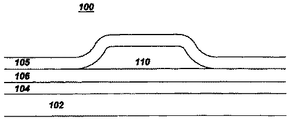
ここで添付図面、特に図1を参照すると、これらの図解は本発明の好適な実施形態を具体的に記述するためのもので、本発明を限定するものではない。図1は、本発明の物品100の概略図である。物品100は、基材102及び基材102の表面に設けられた1以上のバリヤ層106を備える。所望に応じて、追加の層104、例えば接着層(これに限らない)を基材102と1以上のバリヤ層106との間に設けることができる。基材102はガラス、ポリマー材料、ケイ素、金属ウェッブ及びガラス繊維の1つから構成することができる。基材102がポリマー材料である場合、基材102はポリカーボネート、ポリエチレンテレフタレン、ポリエチレンナフタレン、ポリイミド、ポリエーテルスルホン、ポリアクリレート、ポリノルボルネン及びこれらの組合せの少なくとも1種を含有する。別の実施形態では、基材102はアルミニウム及び鋼の1種からなる金属ウェッブである。
【0020】
1以上のバリヤ層106は、無機材料を含有し、水分及び酸素の透過に抵抗性である(耐水分透過性及び耐酸素透過性)。1以上のバリヤ層106は、25℃、相対湿度100%での水蒸気透過率(WVTR)が約2g/m2日未満であり、25℃、酸素濃度100%での酸素透過率(OTR)が約2cc/m2日未満である。第2の実施形態では、1以上の水分バリヤ層106は、25℃、相対湿度100%での水蒸気透過率が約1.7g/m2日未満であり、25℃、酸素濃度100%での酸素透過率が約0.21cc/m2日未満である。第3の実施形態では、1以上のバリヤ層106は、25℃、相対湿度100%での水蒸気透過率が約0.157g/m2日未満であり、25℃、酸素濃度100%での酸素透過率が約0.13cc/m2日未満である。1以上のバリヤ層106は、金属酸化物、金属窒化物、金属炭化物及びこれらの組合せの少なくとも1つを含有し、その金属はケイ素、アルミニウム、亜鉛、インジウム、錫、遷移金属(例えばチタンなど)の1種である。1実施形態では、1以上のバリヤ層106が酸化チタンを含有する。別の実施形態では、1以上のバリヤ層106が窒化ケイ素を含有する。1以上のバリヤ層106は厚さが約10nm〜約10000nmの範囲にある。1実施形態では、1以上のバリヤ層は厚さが約20nm〜約500nmの範囲にある。
【0021】
物品100はさらに、1以上のバリヤ層106に隣接して設けられた1以上の層110を含んでもよい。物品100がLCDディスプレイである場合、この1以上の層は、錫、カドミウム、インジウム、亜鉛、マグネシウム、ガリウム及びこれらの組合せの酸化物を含有する1以上の透明な導電層を含むことができる。物品100がLED又はOELDである場合、1以上の層は、例えば、陰極層、電子輸送層、発光層(OELDの場合)、正孔輸送層及び陽極層を含むことができ、ここで電子輸送層及び正孔輸送層は有機材料でも無機材料でもよく、発光層は有機材料を含有する。
【0022】
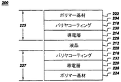
図2は本発明の可撓性液晶ディスプレイの構造を示す概略図である。可撓性LCD200は、中心液晶層212、第1導電層214、第2導電層216、第1バリヤ層218、第2バリヤ層220、第1ポリマー基材222及び第2ポリマー基材224を備える。第1ポリマー基材222、第1導電層214及び第1バリヤ層218の組合せで第1プレート225を形成し、第2ポリマー基材224、第2導電層216及び第2バリヤ層220の組合せで第2プレート227を形成する。第1プレート225及び第2プレート227は互いにほぼ平行に配置され、その間に液晶層212が介在する。可撓性LCDは、本明細書に援用する、Argemiro Soares DaSilva Sobrinhoの米国特許出願第09/836657号「A Transparent Flexible Barrier for Liquid Crystal Display Devices and Method of Making the Same」に記載されている。
【0023】
図3a及び図3bはそれぞれ発光ダイオード(LED)及び有機EL素子(OELD)の概略図である。LED300(図3a)では、バリヤ層312は基材310上に設けられる。陽極314が基材310とは反対側のバリヤ層312の上に設けられる。正孔輸送層314は、当業界で周知の少なくとも1種のn型(負電荷受容性)半導体、例えばリンをドープしたケイ素などを含有し、陽極314の上に、それと接して設けられる。電子輸送層316は、当業界で周知の少なくとも1種のp型(正孔)半導体、例えばアルミニウムをドープしたケイ素などを含有し、正孔輸送層314の上に、それと接して設けられる。陰極318は電子輸送層316の上に、それと接して設けられる。
【0024】
OELD350(図3b)は、基材360、バリヤ層362、陽極364、正孔輸送層366、電子輸送層370及び陰極372を、発光層368が正孔輸送層366と電子輸送層370との間に配置されること以外は、LED300の場合とほぼ同じ関係で含む。正孔輸送層366、発光層368及び電子輸送層370はそれぞれ分子形態又はポリマー形態の有機材料を含有する。電子輸送層370及び発光層368を組合せて単一層としてもよい。或いは、正孔輸送層366、発光層368及び電子輸送層370を組合せて単一層としてもよい。
【0025】
別の実施形態では、1以上の層110は、接着層、耐摩耗性層、紫外線吸収層及び赤外線反射層の少なくとも1層を含んでもよい。1以上の層110が、バリヤ層106の基材102への密着性を高めるための接着層を含む場合、その接着層は元素形態の金属、金属炭化物、金属酸炭化物、金属酸化物、金属窒化物、金属酸窒化物及び金属炭窒化物の少なくとも1種を含有する。ここで金属は、ケイ素、アルミニウム、チタン、ジルコニウム、ハフニウム、タンタル、ガリウム、ゲルマニウム、亜鉛、錫、カドミウム、タングステン、モリブデン、クロム、バナジウム及び白金の1種である。或いは、接着層は、無定形炭素;ガラス、シリカ、アルミナ、ジルコニア、窒化ホウ素、炭化ホウ素、炭窒化ホウ素の少なくとも1種を含有するセラミック材料;シリコーン;モノマー;オリゴマー;シロキサン;ポリマー;エポキシド;アクリレート;アクリロニトリル;キシレン;スチレンなど及びこれらの組合せのうち少なくとも1つを含有してもよい。紫外線吸収層が1以上の層110に含まれる場合、紫外線吸収層は酸化チタン、酸化亜鉛、酸化セリウム、ポリマー又は分子形態の紫外線吸収性有機材料及びこれらの組合せのうち少なくとも1つを含有する。赤外線反射層が1以上の層110に含まれる場合、赤外線反射層は、銀、アルミニウム、インジウム、錫、酸化インジウム錫(ITO)、錫酸カドミウム、亜鉛及びこれらの組合せのうち少なくとも1つを含有する。
【0026】
1実施形態において、1以上のバリヤ層106が1以上の層110と基材102との間に介在する。図1に示す実施形態では、1以上の層110をバリヤ層106と第2バリヤ層105との間に設けてもよい。さらに1以上の層110は、図1に示すように、バリヤ層106の一部と第2バリヤ層105との間に配置する必要があるだけである。このような構成により、水蒸気及び酸素への露出からの1以上の層110の全体的なカプセル封止及び保護を達成する。別の実施形態では、1以上の層110が、図1に104で示されるように、1以上のバリヤ層106と基材102との間に介在する。後者の実施形態の1例は、1以上の層110が接着層を含む場合である。
【0027】
本発明は、前述したバリヤ層106が基材102上に設けられた物品100の形成方法、並びに前述したバリヤ層106を基材102上に形成する方法も包含する。バリヤ層106を基材102上に形成するには、1以上のプラズマ源により発生させたプラズマ中に少なくとも1種の反応物質を注入する。1以上のプラズマ源は、膨張性熱プラズマ(以下「ETP」ともいう)を発生する膨張性熱プラズマ源であるのが好ましい。プラズマを発生するのに、単一プラズマ源を用いても、複数のプラズマ源の配列体を用いてもよい。単一及び複数のプラズマ源を有するシステムが、本明細書に先行技術として援用する、Barry Lee−Mean Yangらの米国特許第6110544号「Protective Coating by High Rate Arc Plasma Deposition」、Barry Lee−Mean Yangらの米国特許出願第06/681820号「Apparatus and Method for Large Area Chemical Vapor Deposition Using Expanding Thermal Plasma Generators」、Marc Schaepkensの米国特許出願第09/683149号「Large Area Plasma Coating Using Multiple Expanding Thermal Plasma Sources in Combination with a Common Injection Source」及びMarc Schaepkensの米国特許出願第09/683148号「Apparatus and Method for Depositing Large Area Coatings on Non−Planar Surfaces」に記載されている。
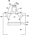
【0028】
図4に、単一ETP源を有するETP堆積システムの概略図を示す。ETP堆積システム400は高圧プラズマ室410及び低圧堆積室420を含み、堆積室420に基材424が収容される。ETP源402は、陰極404、陽極406及びプラズマ源ガス入口408を含み、このうち後者の2つはプラズマ室410に配置されている。プラズマ源ガスは不活性ガス、例えば希ガス、即ちアルゴン、ヘリウム、ネオン、クリプトン又はキセノンである。或いは、化学的反応性ガス、例えば窒素、水素などをプラズマ源ガスとして用いてもよい。アルゴンをプラズマ源ガスとして用いるのが好ましい。陰極404と陽極406との間にアークを発生し、プラズマ源ガス入口408からプラズマ源ガスをアークに導入することにより、膨張性熱プラズマであるプラズマ412をETP源402で発生する。
【0029】
プラズマ室410及び堆積室420は開口418を介して互いに流体連通している。堆積室420は真空系(図示せず)と流体連通している。真空系は、堆積室420をプラズマ室410の圧力よりも低い圧力に維持することができる。1実施形態では、堆積室420を約1トル(約133Pa)未満の圧力、好ましくは約100ミリトル(約0.133Pa)未満の圧力に維持する一方、プラズマ室410を約0.1気圧(約1.01x10⁴Pa)以上の圧力に維持する。
【0030】
少なくとも1種の反応物質ガスを所定の流量でプラズマ源402により発生したプラズマ中に供給するための、1以上の反応物質ガスインジェクタ422が堆積室420に配置されている。プラズマ412が開口418から堆積室420に進入するにつれて、少なくとも1種の反応物質ガスを1以上の反応物質ガスインジェクタ422からプラズマ412に供給する。少なくとも1種の反応物質ガスは、単一の反応物質ガスでも複数の反応物質ガスの混合物でもよい。少なくとも1種の反応物質ガスは、単一の反応物質ガス源又は複数の別々の反応物質源から単一の反応物質ガスインジェクタ系又は複数の別々の反応物質ガスインジェクタ系に供給すればよい。
【0031】
ETPでは、陰極及び陽極間に発生したアーク中でプラズマ源ガスをイオン化し、陽イオンと電子を生成することによりプラズマを発生する。例えば、アルゴンプラズマを発生させる場合、下記の反応が起こる。
【0032】
Ar → Ar++e−
次にプラズマを低圧で大きな体積に膨張させ、これにより電子及び陽イオンを冷却する。本発明では、プラズマ412をプラズマ室410で発生し、開口418を介して堆積室420中に膨張させる。前述したように、堆積室420はプラズマ室410よりも著しく低い圧力に維持されている。その結果、ETP中の電子は冷たすぎ、そのエネルギーはETP内の少なくとも1種の反応物質ガスの解離を直接引き起こすには不十分である。その代わり、プラズマ中に導入された少なくとも1種の反応物質ガスは、ETP内のイオン及び電子との電荷交換反応及び解離的再結合反応を生じ、少なくとも1種の堆積前駆物質を形成する。膨張ETP内で、陽イオン及び電子の温度はほぼ等しく、約0.1eV(約1000K)の範囲にある。ETPとは対照的に、他のタイプのプラズマは、プラズマの化学に有意な影響を与える十分高い温度を有する電子を生成する。このようなプラズマでは、通例陽イオンの温度は0.1eVを上回り、電子の温度は1eV以上、即ち約10000K以上である。
【0033】
プラズマ412に注入されると、少なくとも1種の反応物質ガスはETP内で反応して少なくとも1種の堆積前駆物質を形成する。このような反応には、電荷交換反応、解離的再結合反応、フラグメント化反応があるが、これらに限定されない。この後ETP内に形成された少なくとも1種の堆積前駆物質が、基材424の表面上に堆積して基材424上にバリヤ層106を形成する。
【0034】
少なくとも1種の堆積前駆物質は基材424上に約200nm/min以上の速度で堆積して基材424上に1以上のバリヤ層106を形成するが、それより高い堆積速度も本発明の範囲内である。例えば1実施形態では、少なくとも1種の堆積前駆物質を約600nm/min以上の速度で基材424上に堆積する。別の実施形態では、少なくとも1種の堆積前駆物質を約3000nm/min以上の速度で基材424上に堆積する。さらに他の実施形態では、少なくとも1種の堆積前駆物質を約10000nm/min以上の速度で基材424の表面上に堆積する。
【0035】
前述したように、1以上のバリヤ層106は、金属酸化物、金属窒化物、金属炭化物及びこれらの組合せの少なくとも1種を含有し、その金属はケイ素、アルミニウム、亜鉛、インジウム、錫及び遷移金属(例えばチタンなど)の1種である。これらの例において、少なくとも1種の反応物質ガスは、シラン、金属蒸気、金属ハロゲン化物及び金属の有機化合物の少なくとも1種を含有する第1気体状反応物質を含み、その金属はチタン、亜鉛、アルミニウム、インジウム及び錫の1種である。シランの例としては、ジシラン、アミノシラン及びクロロシランがある。有機化合物の例としては、チタンイソプロポキシド、ジエチル亜鉛、ジメチル亜鉛、インジウムイソプロポキシド、インジウムtert−ブトキシド、アルミニウムイソプロポキシド及びこれらの組合せがある。金属ハロゲン化物の例としては、チタン、錫及びアルミニウムの塩化物がある。少なくとも1種の反応物質は、蒸気状態の元素亜鉛、インジウム、錫及びアルミニウムを含有してもよい。第1気体状反応物質をプラズマ412中に、酸素、窒素、水素、水及びアンモニアの少なくとも1種を含有する第2気体状反応物質と共に注入する。1以上のバリヤ層106がチタンの酸化物、窒化物及び炭化物の少なくとも1種を含有する実施形態では、塩化チタン及びチタンイソプロポキシドの少なくとも1種を含有する第1気体状反応物質をプラズマ412中に第2反応物質と共に注入する。ここで第2反応物質は、酸素、窒素、水素、水及びアンモニアの代わりに或いはそれに加えて、プロパン、ブタン、アセチレンなど及びこれらの組合せを含有してもよい。1以上のバリヤ層106がケイ素の酸化物、窒化物及び炭化物の少なくとも1種を含有する別の実施形態では、シラン、ジシラン、アミノシラン及びクロロシランの少なくとも1種を含有する第1気体状反応物質をプラズマ412中に第2反応物質と共に注入する。例えば、ヘリウムで濃度約2%に希釈したシラン(SiH4)とアンモニアを膨張性熱アルゴンプラズマ中に注入することにより、窒化ケイ素バリヤ層を堆積することができる。
【0036】
前述したように、物品100は、1以上のバリヤ層106に加えて、さらに1以上の層110を含んでもよい。このような場合、上述した、バリヤ層106を基材102上に配置した物品100の形成方法及びバリヤ層106を基材102上に形成する方法は、さらに、その1以上の層110を基材102又はバリヤ層106いずれかに被覆する1以上の工程を含む。1以上の層110を堆積する方法はその1以上のコーティングの性質や特性(例えば組成、所望の物性など)に依存することが、当業者には明らかである。1以上の層110は、上述したETPプラズマ装置及び方法を用いて堆積することができる。或いは、スパッタリング、蒸着、イオンビームアシスト堆積(IBAD)、プラズマ利用化学蒸着(PECVD)、誘導結合プラズマ(ICP)又は電子サイクロトロン共鳴(ECR)いずれかを用いる高強度プラズマ化学蒸着(HIPCVD)などの方法を用いて、1以上の層110を堆積してもよい。
【実施例】
【0037】
以下に実施例を示して本発明の特徴と効果を具体的に説明する。
実施例1
厚さ30ミル(約0.76mm)のポリカーボネート基材を、本明細書に記載し、図4に概略を示したシステムと同様のプラズマ堆積システムの堆積室に入れた。基材を、膨張性熱プラズマ(ETP)から約25〜60cmの範囲の作用距離(WD)に配置した。真空容器を約100ミリトル(mTorr)未満の圧力まで排気し、アルゴンガスをプラズマ室及びETP源に約2〜3slm(standard liters per minute)の範囲の流量で流し、プラズマ源を付勢した。ETPの生成は約40〜70Aの範囲の電流レベルで行った。プラズマ室内の圧力を約300〜800トルの範囲とし、一方堆積室内の圧力を約45〜100ミリトルの範囲とした。この圧力差のため、アルゴン熱プラズマは堆積室に向かって膨張した。堆積室では、ヘリウムで濃度約2%に希釈したシランとアンモニアからなる反応物質をリングインジェクタを介して膨張性熱アルゴンプラズマ中に注入した。反応物質がETPと反応して堆積前駆物質を形成し、これらが化合してポリカーボネート基材上に200nm/min以上の堆積速度で窒化ケイ素材料バリヤ層を堆積した。
【0038】
窒化ケイ素バリヤ層の25℃、相対湿度100%での水蒸気透過率(WVTR)を反応物質(本例ではアンモニア)の流量の関数としてプロットしたグラフを図5に示す。厚さ30ミルの未被覆ポリカーボネートフィルムの水蒸気透過率も図5に示す。図5から明らかなように、厚さ約30ミルのポリカーボネートフィルム上に堆積した厚さ350nmの単一窒化ケイ素バリヤ層は、水蒸気透過率を0.2g/m2日未満に減らす。これらのフィルムは高度に透明かつ無色であり、窒化ケイ素バリヤ層で被覆されたポリカーボネートフィルムは透明度89%以上、黄色度指数0.7未満である。
【0039】
以上、代表的な実施形態を具体的な説明のために記載したが、上述の説明は本発明の範囲を限定すると考えるべきではない。例えば、基材及び上述した特性を有するバリヤ層を備える、可撓性LCDディスプレイ、LED及びOELD以外の物品も、本発明の範囲に包含されるものである。このような物品には、光起電力素子、エレクトロクロミック素子、X線撮像素子、有機集積回路及び硬質基材ディスプレイ素子などがある。したがって、当業者であれば、本発明の要旨から逸脱することなく種々の変更、改変、置き換えが可能である。
【図面の簡単な説明】
【0040】
【図1】本発明の物品の概略図である。
【図2】本発明の可撓性液晶ディスプレイの概略図である。
【図3a】本発明の発光ダイオードの概略図である。
【図3b】本発明の有機EL素子の概略図である。
【図4】膨張性熱プラズマ堆積システムの概略図である。
【図5】本発明の窒化ケイ素バリヤ層の水蒸気透過率を反応物質流量の関数として示すグラフである。
【符号の説明】
【0041】
100 物品
102 基材
104 接着層
105 第2バリヤ層
106 バリヤ層
110 1以上の層【Technical field】
[0001]
The present invention relates to a barrier layer having excellent resistance to permeation of moisture and oxygen. The invention particularly relates to articles having such a barrier layer and to a method of applying a barrier layer to an article.
[Background Art]
[0002]
Various types of electronic devices, such as light emitting diodes (hereinafter "LED"), liquid crystal displays (hereinafter "LCD"), photovoltaic articles, flat panel display devices, electrochromic articles, and organic EL devices (hereinafter "OELD"). They share the same architecture. That is, each device includes one or more substrates and one or more "active" layers.
[0003]
Many of the materials used for the active layers of such devices are sensitive to environmental factors. Electrode materials for LEDs and OELDs are sensitive to air and moisture, as are polymers and organic compounds used for OELDs and liquid crystal materials used for LCDs. Exposure to weather, especially oxygen and water, can severely limit the life of such devices.
[0004]
The choice of a substantially impermeable substrate, such as glass, protects against environmental attack. However, the polymer substrate used in such flexible devices does not provide adequate protection against oxygen and moisture. As a result, the polymer substrate must be provided with one or more coatings that are substantially impermeable to oxygen and water vapor to achieve the desired level of protection.
[0005]
The barrier material is applied to the substrate using various coating methods. For example, plasma enhanced chemical vapor deposition (PECVD) has been used to deposit barrier materials. However, typical PECVD methods are relatively slow. That is, the rate at which the barrier material is deposited on the substrate is about 30 to 60 nm / min or less. To be commercially viable, barrier coatings must be applied to substrates at higher deposition rates.
[Disclosure of Invention]
[Problems to be solved by the invention]
[0006]
Barrier materials are needed to extend the life of flexible display devices, such as LCDs, LEDs, OELDs, etc. to acceptable levels, but the methods currently used to apply the necessary barrier materials to substrates. Is too slow. Therefore, there is a need for a method of forming a barrier layer on a substrate at a high deposition rate. There is also a need for a method of forming a barrier layer on a substrate to produce an article having an acceptable water vapor and oxygen permeability. Further, there is a need for an article having a barrier layer that has acceptable water vapor and oxygen transmission rates.
[Means for Solving the Problems]
[0007]
In order to meet the above-mentioned demands, the present invention provides an article comprising a substrate and a barrier layer provided on the surface of the substrate, the barrier layer being resistant to permeation of moisture and oxygen, and such a barrier layer formed on the substrate. A method for depositing is provided. The article may include additional layers, such as an adhesive layer, an abrasion resistant layer, a radiation absorbing layer, a radiation reflecting layer, a conductive layer, and the like. Such articles include, but are not limited to, light emitting diodes (LEDs), liquid crystal displays (LCDs), photovoltaic articles, electrochromic articles, organic integrated circuits, organic EL devices (OELD), and the like.
[0008]
Therefore, the first invention provides an article. The article comprises a substrate and one or more barrier layers provided on at least one surface of the substrate, wherein the barrier layer comprises an inorganic material, and wherein the barrier layer is resistant to permeation of moisture and oxygen; Water vapor transmission rate (WVTR) at 100 ° C. and 100% relative humidity is about 2 g / m2Less than 2 days, and the oxygen transmission rate (OTR) at 25 ° C. and 100% oxygen concentration is about 2 cc / m2Less than a day.
[0009]
A second invention provides a barrier layer that is resistant to permeation of moisture and oxygen. The barrier layer contains at least one of a metal oxide, a metal nitride, a metal carbide, and combinations thereof. Each of the metal nitrides, metal carbides and metal oxides contains at least one of silicon, aluminum, zinc, indium, tin, transition metals and combinations thereof. The barrier
The layer has a water vapor transmission rate (WVTR) of about 2 g /
Oxygen permeability (OTR) at 25 ° C and 100% oxygen concentration is about 2cc / m2Less than a day.
[0010]
A third invention provides an article. The article comprises a substrate and one or more barrier layers, wherein the barrier layer comprises at least one of a metal oxide, a metal nitride, a metal carbide, and combinations thereof, wherein the metal nitride, the metal carbide, and the metal Each of the oxides contains at least one of silicon, aluminum, zinc, indium, tin, transition metals and combinations thereof, and the barrier layer is resistant to permeation of moisture and oxygen; % Water vapor transmission rate (WVTR) is about 2 g / m2Less than 2 days, and the oxygen transmission rate (OTR) at 25 ° C. and 100% oxygen concentration is about 2 cc / m2Less than a day.
[0011]
A fourth invention provides a method for forming a coated article. The coated article comprises a substrate and a barrier layer disposed thereon, said barrier layer being moisture and oxygen permeable and having a water vapor transmission rate (WVTR) at 25 ° C. and 100% relative humidity of about 2 g. / M2Less than 2 days, and the oxygen transmission rate (OTR) at 25 ° C. and 100% oxygen concentration is about 2 cc / m2Less than a day. The method includes providing a substrate, generating a thermal plasma having an electron temperature of less than about 1 eV, injecting at least one reactant into the thermal plasma, and incorporating the at least one reactant into the inflatable thermal plasma. Forming at least one deposition precursor on said substrate by depositing said at least one deposition precursor on said substrate at a rate of at least about 200 nm / min. including.
[0012]
A fifth invention provides a method for forming a barrier layer on a substrate. The barrier layer is resistant to permeation of moisture and oxygen and has a water vapor transmission rate (WVTR) of about 2 g /
[0013]
A sixth invention provides a method for forming a coated article. The coated article comprises a substrate and a barrier layer provided thereon. The barrier layer is resistant to permeation of moisture and oxygen and has a water vapor transmission rate (WVTR) of about 2 g /
[0014]
The above and other aspects, advantages and features of the present invention will become apparent from the following detailed description, the accompanying drawings and the appended claims.
BEST MODE FOR CARRYING OUT THE INVENTION
[0015]
In the following description, the same reference numerals indicate the same or corresponding parts throughout the several drawings. In addition, terms such as “up,” “down,” “outside,” and “inside” are terms used for convenience and should not be construed as limiting.
[0016]
Various display devices, for example, a light emitting diode (hereinafter also referred to as “LED”), a liquid crystal display (hereinafter also referred to as “LCD”), a photovoltaic product, a flat panel display device, an electrochromic product, and an organic EL device (hereinafter “OELD”) ) Share the same architecture. That is, each device includes one or more substrates and one or more "active" layers. For example, a light emitting diode and an organic EL element can have a configuration in which a cathode layer, an electron transport layer, a light emitting layer, a hole transport layer, and an anode layer are stacked on a base material. The liquid crystal display may include two substrates each provided with a conductive layer, and may have a configuration in which a liquid crystal layer is sandwiched between the two substrates.
[0017]
Many of the materials used in these devices can be adversely affected by environmental factors. Electrode materials for LEDs and OELDs are sensitive to air and moisture, as are polymers and organic compounds used for OELDs and liquid crystal materials used for LCDs. Exposure to weather, especially oxygen and water, can severely limit the life of such devices.
[0018]
The choice of a substantially impermeable substrate, such as glass, protects against environmental attack. However, the polymer substrate used in such flexible devices does not provide adequate protection against oxygen and moisture. As a result, the polymer substrate must be provided with one or more barrier layers that are substantially impermeable to oxygen and water vapor to achieve the desired level of protection. Here, the coating, apparatus or coated substrate described as “almost impermeable” has a water vapor transmission rate (hereinafter also referred to as “WVTR”) at 25 ° C. and 100% relative humidity of about 2 g / m 2.2Days, the oxygen transmission rate (hereinafter also referred to as “OTR”) at 25 ° C. and an oxygen concentration of 100% is about 2 cc / m 2.2Means less than days.
[0019]
Referring now to the accompanying drawings, and in particular to FIG. 1, these illustrations are intended to describe preferred embodiments of the invention in detail and are not intended to limit the invention. FIG. 1 is a schematic diagram of an
[0020]
One or more barrier layers 106 contain an inorganic material and are resistant to permeation of moisture and oxygen (moisture permeation resistance and oxygen permeation resistance). One or more barrier layers 106 have a water vapor transmission rate (WVTR) of about 2 g /
[0021]
[0022]
FIG. 2 is a schematic view showing the structure of the flexible liquid crystal display of the present invention. The
[0023]
3a and 3b are schematic diagrams of a light emitting diode (LED) and an organic EL device (OELD), respectively. In the LED 300 (FIG. 3a), the
[0024]
The OELD 350 (FIG. 3b) includes a
[0025]
In another embodiment, one or
[0026]
In one embodiment, one or more barrier layers 106 intervene between one or
[0027]
The present invention also includes a method for forming the
[0028]
FIG. 4 shows a schematic diagram of an ETP deposition system having a single ETP source. The
[0029]
[0030]
One or more
[0031]
In ETP, a plasma is generated by ionizing a plasma source gas in an arc generated between a cathode and an anode to generate positive ions and electrons. For example, when generating argon plasma, the following reaction occurs.
[0032]
Ar → Ar++ E−
The plasma is then expanded to a large volume at low pressure, thereby cooling the electrons and cations. In the present invention, a
[0033]
When injected into the
[0034]
At least one deposition precursor is deposited on the
[0035]
As described above, the one or more barrier layers 106 include at least one of a metal oxide, a metal nitride, a metal carbide, and combinations thereof, wherein the metal is silicon, aluminum, zinc, indium, tin, and a transition metal. (For example, titanium). In these examples, the at least one reactant gas comprises a first gaseous reactant containing at least one of silane, metal vapor, metal halide and an organic compound of a metal, wherein the metal is titanium, zinc, One of aluminum, indium and tin. Examples of silanes include disilane, aminosilane and chlorosilane. Examples of organic compounds include titanium isopropoxide, diethyl zinc, dimethyl zinc, indium isopropoxide, indium tert-butoxide, aluminum isopropoxide and combinations thereof. Examples of metal halides include titanium, tin and aluminum chlorides. The at least one reactant may contain the elements zinc, indium, tin and aluminum in the vapor state. A first gaseous reactant is injected into the
[0036]
As mentioned above, the
【Example】
[0037]
Hereinafter, the features and effects of the present invention will be specifically described with reference to examples.
Example 1
A 30 mil (approximately 0.76 mm) thick polycarbonate substrate was placed in the deposition chamber of a plasma deposition system similar to the system described herein and schematically illustrated in FIG. The substrate was placed at a working distance (WD) in the range of about 25-60 cm from the expansive thermal plasma (ETP). The vacuum vessel was evacuated to a pressure of less than about 100 millitorr (mTorr), and argon gas was flowed through the plasma chamber and ETP source at a flow rate in the range of about 2-3 slm (standard liters per minute) to energize the plasma source. ETP generation was performed at current levels in the range of about 40-70A. The pressure in the plasma chamber was in the range of about 300-800 Torr, while the pressure in the deposition chamber was in the range of about 45-100 mTorr. Due to this pressure difference, the argon thermal plasma expanded toward the deposition chamber. In the deposition chamber, a reactant consisting of silane and ammonia diluted to a concentration of about 2% with helium was injected into the expansive hot argon plasma via a ring injector. The reactants reacted with the ETP to form deposition precursors, which combined to deposit a silicon nitride material barrier layer on the polycarbonate substrate at a deposition rate of 200 nm / min or more.
[0038]
FIG. 5 shows a graph plotting the water vapor transmission rate (WVTR) of the silicon nitride barrier layer at 25 ° C. and 100% relative humidity as a function of the flow rate of the reactant (ammonia in this example). The water vapor transmission rate of a 30 mil thick uncoated polycarbonate film is also shown in FIG. As can be seen from FIG. 5, a single 350 nm thick silicon nitride barrier layer deposited on a polycarbonate film about 30 mils thick has a water vapor transmission rate of 0.2 g / m2.2Reduce to less than a day. These films are highly transparent and colorless and polycarbonate films coated with a silicon nitride barrier layer have a transparency of 89% or more and a yellowness index of less than 0.7.
[0039]
While the exemplary embodiments have been described for specific description, the above description should not be considered as limiting the scope of the present invention. For example, articles other than flexible LCD displays, LEDs, and OELDs, comprising a substrate and a barrier layer having the properties described above, are also within the scope of the invention. Such articles include photovoltaic devices, electrochromic devices, X-ray imaging devices, organic integrated circuits, and rigid substrate display devices. Therefore, those skilled in the art can make various changes, modifications, and substitutions without departing from the gist of the present invention.
[Brief description of the drawings]
[0040]
FIG. 1 is a schematic view of an article of the present invention.
FIG. 2 is a schematic view of a flexible liquid crystal display of the present invention.
FIG. 3a is a schematic diagram of a light emitting diode of the present invention.
FIG. 3b is a schematic view of the organic EL device of the present invention.
FIG. 4 is a schematic diagram of an inflatable thermal plasma deposition system.
FIG. 5 is a graph showing the water vapor transmission rate of a silicon nitride barrier layer of the present invention as a function of reactant flow rate.
[Explanation of symbols]
[0041]
100 articles
102 base material
104 adhesive layer
105 Second barrier layer
106 barrier layer
110 One or more layers
Claims (103)
バリヤ層は無機材料を含有し、またバリヤ層は水分及び酸素の透過抵抗性であり、25℃、相対湿度100%での水蒸気透過率(WVTR)が約2g/m2日未満であり、25℃、酸素濃度100%での酸素透過率(OTR)が約2cc/m2日未満である、物品。An article comprising (a) a base material and (b) one or more barrier layers provided on at least one surface of the base material,
The barrier layer contains an inorganic material, and the barrier layer is resistant to permeation of moisture and oxygen, has a water vapor transmission rate (WVTR) at 25 ° C. and 100% relative humidity of less than about 2 g / m 2 days, An article having an oxygen transmission rate (OTR) of less than about 2 cc / m 2 days at 100 ° C. and 100% oxygen concentration.
前記1以上のバリヤ層は金属酸化物、金属窒化物、金属炭化物及びこれらの組合せの少なくとも1種を含有し、前記金属窒化物、金属炭化物及び金属酸化物のそれぞれがケイ素、アルミニウム、亜鉛、インジウム、錫、遷移金属及びこれらの組合せの少なくとも1種を含有し、また前記バリヤ層は水分及び酸素の透過抵抗性であり、25℃、相対湿度100%での水蒸気透過率(WVTR)が約2g/m2日未満であり、25℃、酸素濃度100%での酸素透過率(OTR)が約2cc/m2日未満である、物品。An article comprising (a) a substrate and (b) one or more barrier layers,
The one or more barrier layers include at least one of a metal oxide, a metal nitride, a metal carbide, and combinations thereof, wherein each of the metal nitride, metal carbide, and metal oxide is silicon, aluminum, zinc, indium. , Tin, transition metals and combinations thereof, and the barrier layer is moisture and oxygen permeable and has a water vapor transmission rate (WVTR) at 25 ° C. and 100% relative humidity of about 2 g. / m is less than 2 days, less than 25 ° C., the oxygen permeability of an oxygen concentration 100% (OTR) of about 2 cc / m 2 day, article.
(a)基材を用意し、
(b)電子温度約1eV未満の熱プラズマを発生し、
(c)少なくとも1種の反応物質を熱プラズマ中に注入し、
(d)前記反応物質を前記膨張性熱プラズマ中で反応させて少なくとも1種の堆積前駆物質を形成し、
(e)前記少なくとも1種の堆積前駆物質を前記基材上に約200nm/min以上の速度で堆積してバリヤ層を基材上に形成する
工程を含む方法。A substrate and a barrier layer disposed thereon, wherein the barrier layer is resistant to permeation of moisture and oxygen and has a water vapor transmission rate (WVTR) at 25 ° C. and 100% relative humidity of about 2 g / m 2. Less than about 2 days, wherein the oxygen transmission rate (OTR) at 25 ° C. and 100% oxygen concentration is less than about 2 cc / m 2 days, comprising:
(A) Prepare a base material,
(B) generating thermal plasma having an electron temperature of less than about 1 eV;
(C) injecting at least one reactant into a thermal plasma;
(D) reacting the reactants in the expanding thermal plasma to form at least one deposition precursor;
(E) depositing the at least one deposition precursor on the substrate at a rate of about 200 nm / min or more to form a barrier layer on the substrate.
(a)電子温度約1eV未満の熱プラズマを発生し、
(b)ケイ素、アルミニウム、亜鉛、インジウム、錫、遷移金属及びこれらの組合せの少なくとも1種を含有する第1反応物質を熱プラズマ中に注入し、
(c)酸素、窒素及びアンモニアの少なくとも1種を含有する第2反応物質を熱プラズマ中に注入し、
(d)前記第1反応物質と第2反応物質を前記熱プラズマ中で反応させて少なくとも1種の堆積前駆物質を形成し、
(e)前記少なくとも1種の堆積前駆物質を前記基材上に約200nm/min以上の速度で堆積して、金属酸化物、金属窒化物、金属炭化物及びこれらの組合せの少なくとも1種を含有するバリヤ層を基材上に形成する
工程を含む方法。A method of forming a barrier layer on a substrate, wherein the barrier layer is resistant to permeation of moisture and oxygen and has a water vapor transmission rate (WVTR) at 25 ° C. and 100% relative humidity of about 2 g / m 2 days. Less than about 2 cc / m 2 day at 25 ° C. and 100% oxygen concentration, wherein the barrier layer comprises at least one of a metal oxide, a metal nitride, a metal carbide, and combinations thereof. Wherein each of the metal nitride, metal carbide and metal oxide comprises at least one of silicon, aluminum, zinc, indium, tin, transition metal and combinations thereof,
(A) generating a thermal plasma having an electron temperature of less than about 1 eV;
(B) injecting a first reactant containing at least one of silicon, aluminum, zinc, indium, tin, transition metals and combinations thereof into a thermal plasma;
(C) injecting a second reactant containing at least one of oxygen, nitrogen and ammonia into the thermal plasma;
(D) reacting the first reactant and the second reactant in the thermal plasma to form at least one deposition precursor;
(E) depositing the at least one deposition precursor on the substrate at a rate of about 200 nm / min or more and containing at least one of a metal oxide, a metal nitride, a metal carbide, and a combination thereof; A method comprising forming a barrier layer on a substrate.
(a)基材を用意し、
(b)電子温度約1eV未満の熱プラズマを発生し、
(c)ケイ素、アルミニウム、亜鉛、インジウム、錫、遷移金属及びこれらの組合せの少なくとも1種を含有する第1反応物質を熱プラズマ中に注入し、
(d)酸素、窒素、水及びアンモニアの少なくとも1種を含有する第2反応物質を熱プラズマ中に注入し、
(e)前記第1反応物質と第2反応物質を前記熱プラズマ中で反応させて少なくとも1種の堆積前駆物質を形成し、
(f)前記少なくとも1種の堆積前駆物質を前記基材上に約200nm/min以上の速度で堆積して、金属酸化物、金属窒化物、金属炭化物及びこれらの組合せの少なくとも1種を含有するバリヤ層を基材上に形成する
工程を含む方法。A substrate and a barrier layer provided thereon, wherein the barrier layer has a water vapor transmission rate (WVTR) of less than about 2 g / m 2 day at 25 ° C. and 100% relative humidity; % Oxygen transmission rate (OTR) in less than about 2 cc / m 2 days, wherein the barrier layer comprises at least one of a metal oxide, a metal nitride, a metal carbide, and combinations thereof; A method of forming a coated article, wherein each of the metal carbide and the metal oxide comprises at least one of silicon, aluminum, zinc, indium, tin, transition metals and combinations thereof,
(A) Prepare a base material,
(B) generating thermal plasma having an electron temperature of less than about 1 eV;
(C) injecting a first reactant containing at least one of silicon, aluminum, zinc, indium, tin, transition metals and combinations thereof into a thermal plasma;
(D) injecting a second reactant containing at least one of oxygen, nitrogen, water and ammonia into the thermal plasma;
(E) reacting the first reactant and the second reactant in the thermal plasma to form at least one deposition precursor;
(F) depositing the at least one deposition precursor on the substrate at a rate of about 200 nm / min or more and containing at least one of a metal oxide, a metal nitride, a metal carbide, and a combination thereof; A method comprising forming a barrier layer on a substrate.
Applications Claiming Priority (1)
| Application Number | Priority Date | Filing Date | Title |
|---|---|---|---|
| US10/063,917 US6743524B2 (en) | 2002-05-23 | 2002-05-23 | Barrier layer for an article and method of making said barrier layer by expanding thermal plasma |
Publications (2)
| Publication Number | Publication Date |
|---|---|
| JP2004160977A true JP2004160977A (en) | 2004-06-10 |
| JP2004160977A5 JP2004160977A5 (en) | 2006-07-06 |
Family
ID=29399092
Family Applications (1)
| Application Number | Title | Priority Date | Filing Date |
|---|---|---|---|
| JP2003144218A Pending JP2004160977A (en) | 2002-05-23 | 2003-05-22 | Barrier layer for article and process of forming the barrier layer using expanding thermal plasma |
Country Status (3)
| Country | Link |
|---|---|
| US (3) | US6743524B2 (en) |
| EP (1) | EP1365458A1 (en) |
| JP (1) | JP2004160977A (en) |
Cited By (10)
| Publication number | Priority date | Publication date | Assignee | Title |
|---|---|---|---|---|
| JP2006239883A (en) * | 2005-02-28 | 2006-09-14 | Fuji Photo Film Co Ltd | Steam barrier film |
| JP2008504114A (en) * | 2004-06-25 | 2008-02-14 | アプライド マテリアルズ インコーポレイテッド | Improving the water shielding performance of the encapsulation membrane |
| JP2008532852A (en) * | 2005-03-18 | 2008-08-21 | エクスアテック、エル.エル.シー. | Luminescent plastic window glass |
| JP2008546211A (en) * | 2005-06-10 | 2008-12-18 | ゼネラル・エレクトリック・カンパニイ | Hermetic sealing package and manufacturing method thereof |
| JP2010511975A (en) * | 2006-11-30 | 2010-04-15 | コーニング インコーポレイテッド | Flexible substrate with thin film barrier |
| JP2010215967A (en) * | 2009-03-17 | 2010-09-30 | Fujifilm Corp | Method for manufacturing gas barrier film, gas barrier film for solar battery, and gas barrier film for display |
| JP2012215825A (en) * | 2011-03-25 | 2012-11-08 | Fujifilm Corp | Heat ray shielding member and laminate structure |
| JP2014525647A (en) * | 2011-08-10 | 2014-09-29 | ゼネラル・エレクトリック・カンパニイ | Organic light emitting diode package with energy blocking layer |
| US8901015B2 (en) | 2012-02-15 | 2014-12-02 | Applied Materials, Inc. | Method for depositing an inorganic encapsulating film |
| US9893242B2 (en) | 2015-09-30 | 2018-02-13 | Nichia Corporation | Light emitting device |
Families Citing this family (89)
| Publication number | Priority date | Publication date | Assignee | Title |
|---|---|---|---|---|
| US20090111206A1 (en) | 1999-03-30 | 2009-04-30 | Daniel Luch | Collector grid, electrode structures and interrconnect structures for photovoltaic arrays and methods of manufacture |
| US8138413B2 (en) | 2006-04-13 | 2012-03-20 | Daniel Luch | Collector grid and interconnect structures for photovoltaic arrays and modules |
| US8222513B2 (en) | 2006-04-13 | 2012-07-17 | Daniel Luch | Collector grid, electrode structures and interconnect structures for photovoltaic arrays and methods of manufacture |
| US7507903B2 (en) | 1999-03-30 | 2009-03-24 | Daniel Luch | Substrate and collector grid structures for integrated series connected photovoltaic arrays and process of manufacture of such arrays |
| US8076568B2 (en) * | 2006-04-13 | 2011-12-13 | Daniel Luch | Collector grid and interconnect structures for photovoltaic arrays and modules |
| US8664030B2 (en) | 1999-03-30 | 2014-03-04 | Daniel Luch | Collector grid and interconnect structures for photovoltaic arrays and modules |
| US6866901B2 (en) | 1999-10-25 | 2005-03-15 | Vitex Systems, Inc. | Method for edge sealing barrier films |
| US20100330748A1 (en) | 1999-10-25 | 2010-12-30 | Xi Chu | Method of encapsulating an environmentally sensitive device |
| US7198832B2 (en) | 1999-10-25 | 2007-04-03 | Vitex Systems, Inc. | Method for edge sealing barrier films |
| US7898053B2 (en) | 2000-02-04 | 2011-03-01 | Daniel Luch | Substrate structures for integrated series connected photovoltaic arrays and process of manufacture of such arrays |
| US7898054B2 (en) | 2000-02-04 | 2011-03-01 | Daniel Luch | Substrate structures for integrated series connected photovoltaic arrays and process of manufacture of such arrays |
| US8198696B2 (en) | 2000-02-04 | 2012-06-12 | Daniel Luch | Substrate structures for integrated series connected photovoltaic arrays and process of manufacture of such arrays |
| FR2827396B1 (en) * | 2001-07-12 | 2003-11-14 | Saint Gobain | ELECTRICALLY CONTROLLABLE DEVICE WITH VARIABLE OPTICAL AND / OR ENERGY PROPERTIES |
| US8900366B2 (en) | 2002-04-15 | 2014-12-02 | Samsung Display Co., Ltd. | Apparatus for depositing a multilayer coating on discrete sheets |
| US8808457B2 (en) | 2002-04-15 | 2014-08-19 | Samsung Display Co., Ltd. | Apparatus for depositing a multilayer coating on discrete sheets |
| US20040229051A1 (en) * | 2003-05-15 | 2004-11-18 | General Electric Company | Multilayer coating package on flexible substrates for electro-optical devices |
| US7086918B2 (en) * | 2002-12-11 | 2006-08-08 | Applied Materials, Inc. | Low temperature process for passivation applications |
| US6890656B2 (en) * | 2002-12-20 | 2005-05-10 | General Electric Company | High rate deposition of titanium dioxide |
| US7648925B2 (en) | 2003-04-11 | 2010-01-19 | Vitex Systems, Inc. | Multilayer barrier stacks and methods of making multilayer barrier stacks |
| US7002292B2 (en) * | 2003-07-22 | 2006-02-21 | E. I. Du Pont De Nemours And Company | Organic electronic device |
| DE102004001603B4 (en) * | 2004-01-09 | 2009-03-05 | Schott Ag | Container with interior decor |
| US20050202263A1 (en) * | 2004-03-09 | 2005-09-15 | Jonathan Sargent | Barrier layer to prevent the loss of additives in an underlying layer |
| US7106488B2 (en) * | 2004-03-23 | 2006-09-12 | Air Products And Chemicals, Inc. | Hybrid process for depositing electrochromic coating |
| JP2005285659A (en) * | 2004-03-30 | 2005-10-13 | Toyota Industries Corp | Organic electroluminescence device and its manufacturing method |
| US7695805B2 (en) * | 2004-11-30 | 2010-04-13 | Tdk Corporation | Transparent conductor |
| DE102005025083B4 (en) * | 2005-05-30 | 2007-05-24 | Infineon Technologies Ag | Thermoplastic thermoset composite and method for bonding a thermoplastic material to a thermoset material |
| US20070020451A1 (en) * | 2005-07-20 | 2007-01-25 | 3M Innovative Properties Company | Moisture barrier coatings |
| US7722929B2 (en) | 2005-08-18 | 2010-05-25 | Corning Incorporated | Sealing technique for decreasing the time it takes to hermetically seal a device and the resulting hermetically sealed device |
| US20070040501A1 (en) | 2005-08-18 | 2007-02-22 | Aitken Bruce G | Method for inhibiting oxygen and moisture degradation of a device and the resulting device |
| US7829147B2 (en) | 2005-08-18 | 2010-11-09 | Corning Incorporated | Hermetically sealing a device without a heat treating step and the resulting hermetically sealed device |
| US7767498B2 (en) | 2005-08-25 | 2010-08-03 | Vitex Systems, Inc. | Encapsulated devices and method of making |
| FR2893427B1 (en) * | 2005-11-16 | 2008-01-04 | Saint Gobain | ELECTROCHEMICAL SYSTEM ON PLASTIC |
| US8822810B2 (en) | 2006-04-13 | 2014-09-02 | Daniel Luch | Collector grid and interconnect structures for photovoltaic arrays and modules |
| US9006563B2 (en) | 2006-04-13 | 2015-04-14 | Solannex, Inc. | Collector grid and interconnect structures for photovoltaic arrays and modules |
| US9865758B2 (en) | 2006-04-13 | 2018-01-09 | Daniel Luch | Collector grid and interconnect structures for photovoltaic arrays and modules |
| US8729385B2 (en) | 2006-04-13 | 2014-05-20 | Daniel Luch | Collector grid and interconnect structures for photovoltaic arrays and modules |
| US9236512B2 (en) | 2006-04-13 | 2016-01-12 | Daniel Luch | Collector grid and interconnect structures for photovoltaic arrays and modules |
| US8884155B2 (en) | 2006-04-13 | 2014-11-11 | Daniel Luch | Collector grid and interconnect structures for photovoltaic arrays and modules |
| GB0607743D0 (en) * | 2006-04-20 | 2006-05-31 | Pilkington Plc | Laminated glazing |
| GB0607746D0 (en) * | 2006-04-20 | 2006-05-31 | Pilkington Plc | Glazing |
| US20080006819A1 (en) * | 2006-06-19 | 2008-01-10 | 3M Innovative Properties Company | Moisture barrier coatings for organic light emitting diode devices |
| US20080138538A1 (en) * | 2006-12-06 | 2008-06-12 | General Electric Company | Barrier layer, composite article comprising the same, electroactive device, and method |
| US7667886B2 (en) | 2007-01-22 | 2010-02-23 | E Ink Corporation | Multi-layer sheet for use in electro-optic displays |
| US8241713B2 (en) * | 2007-02-21 | 2012-08-14 | 3M Innovative Properties Company | Moisture barrier coatings for organic light emitting diode devices |
| US20100118376A1 (en) * | 2007-04-09 | 2010-05-13 | Dong-Joo Kwon | Multi-layered photochromic sheet and photochromic glass prepared therefrom |
| WO2009002892A1 (en) * | 2007-06-22 | 2008-12-31 | The Regents Of The University Of Colorado | Protective coatings for organic electronic devices made using atomic layer deposition and molecular layer deposition techniques |
| US20090200553A1 (en) * | 2007-11-30 | 2009-08-13 | Applied Materials, Inc | High temperature thin film transistor on soda lime glass |
| DE212008000087U1 (en) * | 2007-12-14 | 2010-08-12 | Miasole, Santa Clara | Photovoltaic, environmentally protected facility |
| US8628820B2 (en) * | 2008-03-11 | 2014-01-14 | Ppg Industries Ohio, Inc. | Reflective article and method of making a reflective article |
| US20110197947A1 (en) | 2008-03-20 | 2011-08-18 | Miasole | Wire network for interconnecting photovoltaic cells |
| US20100043863A1 (en) * | 2008-03-20 | 2010-02-25 | Miasole | Interconnect assembly |
| US8912429B2 (en) * | 2008-03-20 | 2014-12-16 | Hanergy Holding Group Ltd. | Interconnect assembly |
| US20090283140A1 (en) * | 2008-05-19 | 2009-11-19 | James Freitag | Method of making contact to a solar cell employing a group ibiiiavia compound absorber layer |
| US8207012B2 (en) * | 2008-04-28 | 2012-06-26 | Solopower, Inc. | Method and apparatus for achieving low resistance contact to a metal based thin film solar cell |
| ITMI20081374A1 (en) * | 2008-07-25 | 2010-01-26 | Getters Spa | COMPOSITE ABSORBER OF H2O FOR SEALED MEDICAL DEVICES |
| JP5374980B2 (en) * | 2008-09-10 | 2013-12-25 | ソニー株式会社 | Solid-state imaging device |
| US20100122730A1 (en) * | 2008-11-17 | 2010-05-20 | Corneille Jason S | Power-loss-inhibiting current-collector |
| KR20100071650A (en) * | 2008-12-19 | 2010-06-29 | 삼성전자주식회사 | Gas barrier thin film, electronic device comprising the same, and method for preparing the same |
| US9337446B2 (en) | 2008-12-22 | 2016-05-10 | Samsung Display Co., Ltd. | Encapsulated RGB OLEDs having enhanced optical output |
| US9184410B2 (en) | 2008-12-22 | 2015-11-10 | Samsung Display Co., Ltd. | Encapsulated white OLEDs having enhanced optical output |
| CN101783395A (en) * | 2009-01-20 | 2010-07-21 | 京东方科技集团股份有限公司 | Organic electroluminescence component and manufacturing method thereof |
| TWI391886B (en) * | 2009-06-12 | 2013-04-01 | Au Optronics Corp | Flexible touch display apparatus |
| EP2451991B1 (en) | 2009-07-08 | 2019-07-03 | Aixtron SE | Method for plasma processing |
| US8362356B2 (en) * | 2009-08-13 | 2013-01-29 | Gtat Corporation | Intermetal stack for use in a photovoltaic device |
| WO2011025715A1 (en) * | 2009-08-24 | 2011-03-03 | First Solar, Inc. | Doped transparent conductive oxide |
| US8590338B2 (en) | 2009-12-31 | 2013-11-26 | Samsung Mobile Display Co., Ltd. | Evaporator with internal restriction |
| TWI514608B (en) | 2010-01-14 | 2015-12-21 | Dow Global Technologies Llc | Moisture resistant photovoltaic devices with exposed conductive grid |
| US9059349B2 (en) | 2010-02-09 | 2015-06-16 | Dow Global Technologies Llc | Moisture resistant photovoltaic devices with improved adhesion of barrier film |
| US9061344B1 (en) | 2010-05-26 | 2015-06-23 | Apollo Precision (Fujian) Limited | Apparatuses and methods for fabricating wire current collectors and interconnects for solar cells |
| US8766240B2 (en) | 2010-09-21 | 2014-07-01 | Universal Display Corporation | Permeation barrier for encapsulation of devices and substrates |
| US10026859B2 (en) | 2010-10-04 | 2018-07-17 | Beijing Apollo Ding Rong Solar Technology Co., Ltd. | Small gauge wire solar cell interconnect |
| CN102560490A (en) * | 2010-12-28 | 2012-07-11 | 鸿富锦精密工业(深圳)有限公司 | Antiseptic treatment method for surfaces of aluminum and aluminum alloy and products thereof |
| US8765232B2 (en) | 2011-01-10 | 2014-07-01 | Plasmasi, Inc. | Apparatus and method for dielectric deposition |
| US8951824B1 (en) | 2011-04-08 | 2015-02-10 | Apollo Precision (Fujian) Limited | Adhesives for attaching wire network to photovoltaic cells |
| US9299956B2 (en) | 2012-06-13 | 2016-03-29 | Aixtron, Inc. | Method for deposition of high-performance coatings and encapsulated electronic devices |
| US10526708B2 (en) | 2012-06-19 | 2020-01-07 | Aixtron Se | Methods for forming thin protective and optical layers on substrates |
| US20140048013A1 (en) * | 2012-08-17 | 2014-02-20 | Intermolecular, Inc. | SEED LAYER FOR ZnO AND DOPED-ZnO THIN FILM NUCLEATION AND METHODS OF SEED LAYER DEPOSITION |
| CN104051357B (en) | 2013-03-15 | 2017-04-12 | 财团法人工业技术研究院 | Environmentally sensitive electronic device and packaging method thereof |
| CN105324707B (en) | 2013-06-12 | 2020-06-12 | 唯景公司 | Pretreatment of Transparent Conductive Oxide (TCO) films for improved electrical contact |
| US10712454B2 (en) | 2014-07-25 | 2020-07-14 | General Electric Company | X-ray detectors supported on a substrate having a metal barrier |
| US9513380B2 (en) | 2014-07-25 | 2016-12-06 | General Electric Company | X-ray detectors supported on a substrate having a surrounding metal barrier |
| DE102015102870A1 (en) * | 2015-02-27 | 2016-09-01 | Fraunhofer-Gesellschaft zur Förderung der angewandten Forschung e.V. | Reflector element and method for its production |
| CN109073949B (en) | 2016-04-19 | 2022-01-11 | Sage电致变色显示有限公司 | Electrochromic device including transparent conductive oxide layer and bus bar and method of forming the same |
| JP6907032B2 (en) * | 2017-06-06 | 2021-07-21 | 株式会社ジャパンディスプレイ | Display device and its manufacturing method |
| JP7000581B2 (en) | 2017-09-12 | 2022-01-19 | セイジ・エレクトロクロミクス,インコーポレイテッド | Non-luminous variable transmissive device and how to form it |
| WO2019096991A1 (en) * | 2017-11-20 | 2019-05-23 | Saint-Gobain Glass France | Non-light-emitting, variable transmission device and a process of fabricating the same |
| US11362293B2 (en) * | 2018-05-31 | 2022-06-14 | Massachusetts Institute Of Technology | Interlayers and associated systems, devices, and methods |
| US11028805B2 (en) | 2019-01-09 | 2021-06-08 | Saudi Arabian Oil Company | System and method for on-board catalytic upgrading of hydrocarbon fuels |
| KR102506156B1 (en) * | 2020-11-13 | 2023-03-06 | 한국광기술원 | Solar Cell Module with Holes and Method for Manufacturing the Same |
Family Cites Families (16)
| Publication number | Priority date | Publication date | Assignee | Title |
|---|---|---|---|---|
| US4709991A (en) * | 1983-04-26 | 1987-12-01 | Seiko Epson Kabushiki Kaisha | Liquid crystal display with barrier layer to reduce permeability |
| NL8701530A (en) | 1987-06-30 | 1989-01-16 | Stichting Fund Ond Material | METHOD FOR TREATING SURFACES OF SUBSTRATES USING A PLASMA AND REACTOR FOR CARRYING OUT THAT METHOD |
| CA2044053C (en) | 1990-06-08 | 2001-11-27 | Roger W. Phillips | Barrier film having high colorless transparency and method |
| MX9303141A (en) * | 1992-05-28 | 1994-04-29 | Polar Materials Inc | METHODS AND DEVICES FOR DEPOSITING BARRIER COATINGS. |
| JPH0796977A (en) * | 1993-06-08 | 1995-04-11 | Ajinomoto Co Inc | Double packing material for easily oxidized substance |
| FR2712310B1 (en) | 1993-11-09 | 1995-12-22 | Pechiney Recherche | Transparent barrier barrier coating for flexible packaging plastic film. |
| JP3017912B2 (en) * | 1993-12-13 | 2000-03-13 | シャープ株式会社 | Electrode substrate for liquid crystal display device and liquid crystal display device |
| JPH10154824A (en) * | 1996-11-21 | 1998-06-09 | Nippon Oil Co Ltd | Photoelectric converter |
| JP3290375B2 (en) * | 1997-05-12 | 2002-06-10 | 松下電器産業株式会社 | Organic electroluminescent device |
| US6110544A (en) | 1997-06-26 | 2000-08-29 | General Electric Company | Protective coating by high rate arc plasma deposition |
| EP1014399B1 (en) * | 1998-12-22 | 2006-05-17 | Matsushita Electric Industrial Co., Ltd. | Flexible thin film capacitor and method for producing the same |
| US6355125B1 (en) * | 1999-03-26 | 2002-03-12 | Agfa-Gevaert | Method for making an electric or electronic module comprising a glass laminate |
| US6413645B1 (en) | 2000-04-20 | 2002-07-02 | Battelle Memorial Institute | Ultrabarrier substrates |
| US6468708B1 (en) * | 2000-04-20 | 2002-10-22 | Eastman Kodak Company | Self-contained humidity stabilized imaging media comprising microencapsulated color formers |
| JP4595276B2 (en) * | 2000-12-25 | 2010-12-08 | 東洋製罐株式会社 | Microwave plasma processing method and apparatus |
| EP1597409A1 (en) * | 2003-02-20 | 2005-11-23 | General Electric Company | Apparatus and method for depositing large area coatings on planar surfaces |
-
2002
- 2002-05-23 US US10/063,917 patent/US6743524B2/en not_active Expired - Lifetime
-
2003
- 2003-05-22 JP JP2003144218A patent/JP2004160977A/en active Pending
- 2003-05-23 EP EP20030253239 patent/EP1365458A1/en not_active Withdrawn
-
2004
- 2004-03-16 US US10/802,101 patent/US20040175580A1/en not_active Abandoned
- 2004-03-16 US US10/802,102 patent/US20040175512A1/en not_active Abandoned
Cited By (14)
| Publication number | Priority date | Publication date | Assignee | Title |
|---|---|---|---|---|
| JP2008504114A (en) * | 2004-06-25 | 2008-02-14 | アプライド マテリアルズ インコーポレイテッド | Improving the water shielding performance of the encapsulation membrane |
| JP4573673B2 (en) * | 2005-02-28 | 2010-11-04 | 富士フイルム株式会社 | Water vapor barrier film |
| JP2006239883A (en) * | 2005-02-28 | 2006-09-14 | Fuji Photo Film Co Ltd | Steam barrier film |
| JP2008532852A (en) * | 2005-03-18 | 2008-08-21 | エクスアテック、エル.エル.シー. | Luminescent plastic window glass |
| US9871199B2 (en) | 2005-03-18 | 2018-01-16 | Sabic Global Technologies B.V. | Light emissive plastic glazing having a multilayered configuration for illuminating passenger compartment |
| US9315148B2 (en) | 2005-03-18 | 2016-04-19 | Exatec Llc | Light emissive plastic glazing |
| JP2008546211A (en) * | 2005-06-10 | 2008-12-18 | ゼネラル・エレクトリック・カンパニイ | Hermetic sealing package and manufacturing method thereof |
| JP2010511975A (en) * | 2006-11-30 | 2010-04-15 | コーニング インコーポレイテッド | Flexible substrate with thin film barrier |
| US8455059B2 (en) | 2009-03-17 | 2013-06-04 | Fujifilm Corporation | Method of producing gas barrier layer, gas barrier film for solar batteries and gas barrier film for displays |
| JP2010215967A (en) * | 2009-03-17 | 2010-09-30 | Fujifilm Corp | Method for manufacturing gas barrier film, gas barrier film for solar battery, and gas barrier film for display |
| JP2012215825A (en) * | 2011-03-25 | 2012-11-08 | Fujifilm Corp | Heat ray shielding member and laminate structure |
| JP2014525647A (en) * | 2011-08-10 | 2014-09-29 | ゼネラル・エレクトリック・カンパニイ | Organic light emitting diode package with energy blocking layer |
| US8901015B2 (en) | 2012-02-15 | 2014-12-02 | Applied Materials, Inc. | Method for depositing an inorganic encapsulating film |
| US9893242B2 (en) | 2015-09-30 | 2018-02-13 | Nichia Corporation | Light emitting device |
Also Published As
| Publication number | Publication date |
|---|---|
| US6743524B2 (en) | 2004-06-01 |
| US20040175512A1 (en) | 2004-09-09 |
| US20040175580A1 (en) | 2004-09-09 |
| EP1365458A1 (en) | 2003-11-26 |
| US20030219632A1 (en) | 2003-11-27 |
Similar Documents
| Publication | Publication Date | Title |
|---|---|---|
| JP2004160977A (en) | Barrier layer for article and process of forming the barrier layer using expanding thermal plasma | |
| JP5929775B2 (en) | Gas barrier film, method for producing the same, and electronic device including the gas barrier film | |
| CA2457791C (en) | Coatings with low permeation of gases and vapors | |
| KR101052380B1 (en) | Diffusion barrier coatings having a gradually changing composition and devices comprising the same | |
| KR101423446B1 (en) | Barrier films for plastic substrates fabricated by atomic layer deposition | |
| US20220018022A1 (en) | Multilayer encapsulation thin-film | |
| US9646940B2 (en) | Gas barrier film and electronic device | |
| CN101512728B (en) | Method to improve transmittance of an encapsulating film | |
| JP5473946B2 (en) | Method for manufacturing multilayer stack structure with improved WVTR barrier property | |
| JP5725865B2 (en) | Plasma processing apparatus and method for processing a substrate using an atmospheric pressure glow discharge electrode configuration | |
| CN104115300B (en) | Method for depositing an encapsulating film | |
| US20050172897A1 (en) | Barrier layer process and arrangement | |
| US8034419B2 (en) | Method for making a graded barrier coating | |
| WO2014123201A1 (en) | Gas barrier film and method for manufacturing same | |
| US20080105370A1 (en) | Composite articles having diffusion barriers and devices incorporating the same | |
| US20090110892A1 (en) | System and method for making a graded barrier coating | |
| CN109155343A (en) | The deposition method of the protective film of light emitting diode | |
| CN110010795B (en) | Silicon nitride film, preparation method thereof and packaging structure | |
| JP6926381B2 (en) | Protective film deposition method for light emitting elements | |
| JP5078344B2 (en) | Gas barrier film and manufacturing method thereof | |
| KR101644038B1 (en) | Transparent conductive film, method for manufacturing the same and touch panel containing the same | |
| CN116426010A (en) | Composite film, preparation method thereof and display device | |
| WO2017153747A1 (en) | Barrier coated substrates | |
| JPH10317148A (en) | Manufacture of gas barrier type plastic film |
Legal Events
| Date | Code | Title | Description |
|---|---|---|---|
| A521 | Request for written amendment filed |
Free format text: JAPANESE INTERMEDIATE CODE: A523 Effective date: 20060522 |
|
| A621 | Written request for application examination |
Free format text: JAPANESE INTERMEDIATE CODE: A621 Effective date: 20060522 |
|
| A977 | Report on retrieval |
Free format text: JAPANESE INTERMEDIATE CODE: A971007 Effective date: 20090305 |
|
| A131 | Notification of reasons for refusal |
Free format text: JAPANESE INTERMEDIATE CODE: A131 Effective date: 20090317 |
|
| A02 | Decision of refusal |
Free format text: JAPANESE INTERMEDIATE CODE: A02 Effective date: 20090908 |