JP2004149405A - Oxide porcelain composition, ceramic multi-layer substrate, and ceramic electronic component - Google Patents
Oxide porcelain composition, ceramic multi-layer substrate, and ceramic electronic component Download PDFInfo
- Publication number
- JP2004149405A JP2004149405A JP2003324791A JP2003324791A JP2004149405A JP 2004149405 A JP2004149405 A JP 2004149405A JP 2003324791 A JP2003324791 A JP 2003324791A JP 2003324791 A JP2003324791 A JP 2003324791A JP 2004149405 A JP2004149405 A JP 2004149405A
- Authority
- JP
- Japan
- Prior art keywords
- ceramic
- weight
- porcelain composition
- electronic component
- oxide
- Prior art date
- Legal status (The legal status is an assumption and is not a legal conclusion. Google has not performed a legal analysis and makes no representation as to the accuracy of the status listed.)
- Granted
Links
- 239000000203 mixture Substances 0.000 title claims abstract description 37
- 229910052573 porcelain Inorganic materials 0.000 title claims abstract description 19
- 239000000758 substrate Substances 0.000 title claims abstract description 18
- 239000000919 ceramic Substances 0.000 title claims description 66
- 229910052751 metal Inorganic materials 0.000 claims abstract description 3
- 239000004020 conductor Substances 0.000 claims description 25
- 229910018072 Al 2 O 3 Inorganic materials 0.000 claims description 12
- 239000010949 copper Substances 0.000 claims description 12
- 229910052574 oxide ceramic Inorganic materials 0.000 claims description 11
- 239000011224 oxide ceramic Substances 0.000 claims description 11
- 229910004298 SiO 2 Inorganic materials 0.000 claims description 9
- RYGMFSIKBFXOCR-UHFFFAOYSA-N Copper Chemical compound [Cu] RYGMFSIKBFXOCR-UHFFFAOYSA-N 0.000 claims description 7
- 229910052802 copper Inorganic materials 0.000 claims description 6
- 230000002250 progressing effect Effects 0.000 abstract 1
- 238000010304 firing Methods 0.000 description 17
- 238000005452 bending Methods 0.000 description 13
- 239000002994 raw material Substances 0.000 description 7
- 239000002002 slurry Substances 0.000 description 6
- 239000000843 powder Substances 0.000 description 5
- 239000001257 hydrogen Substances 0.000 description 4
- 229910052739 hydrogen Inorganic materials 0.000 description 4
- 238000000034 method Methods 0.000 description 4
- 230000001590 oxidative effect Effects 0.000 description 4
- 239000002245 particle Substances 0.000 description 4
- 238000007747 plating Methods 0.000 description 4
- YXFVVABEGXRONW-UHFFFAOYSA-N Toluene Chemical compound CC1=CC=CC=C1 YXFVVABEGXRONW-UHFFFAOYSA-N 0.000 description 3
- -1 BaCO 3 Inorganic materials 0.000 description 2
- PXHVJJICTQNCMI-UHFFFAOYSA-N Nickel Chemical compound [Ni] PXHVJJICTQNCMI-UHFFFAOYSA-N 0.000 description 2
- MCMNRKCIXSYSNV-UHFFFAOYSA-N Zirconium dioxide Chemical compound O=[Zr]=O MCMNRKCIXSYSNV-UHFFFAOYSA-N 0.000 description 2
- 150000001875 compounds Chemical class 0.000 description 2
- 230000006866 deterioration Effects 0.000 description 2
- 238000011049 filling Methods 0.000 description 2
- 239000011521 glass Substances 0.000 description 2
- 238000009413 insulation Methods 0.000 description 2
- 238000004519 manufacturing process Methods 0.000 description 2
- 238000007650 screen-printing Methods 0.000 description 2
- 229910000679 solder Inorganic materials 0.000 description 2
- 239000007858 starting material Substances 0.000 description 2
- ZAMOUSCENKQFHK-UHFFFAOYSA-N Chlorine atom Chemical compound [Cl] ZAMOUSCENKQFHK-UHFFFAOYSA-N 0.000 description 1
- ATJFFYVFTNAWJD-UHFFFAOYSA-N Tin Chemical compound [Sn] ATJFFYVFTNAWJD-UHFFFAOYSA-N 0.000 description 1
- 239000011230 binding agent Substances 0.000 description 1
- 230000015572 biosynthetic process Effects 0.000 description 1
- 239000003990 capacitor Substances 0.000 description 1
- 238000006243 chemical reaction Methods 0.000 description 1
- 239000000460 chlorine Substances 0.000 description 1
- 229910052801 chlorine Inorganic materials 0.000 description 1
- 239000002131 composite material Substances 0.000 description 1
- 230000007423 decrease Effects 0.000 description 1
- 230000007547 defect Effects 0.000 description 1
- 238000007606 doctor blade method Methods 0.000 description 1
- 230000000694 effects Effects 0.000 description 1
- 238000009713 electroplating Methods 0.000 description 1
- 230000002708 enhancing effect Effects 0.000 description 1
- 230000004907 flux Effects 0.000 description 1
- 238000001746 injection moulding Methods 0.000 description 1
- 239000012212 insulator Substances 0.000 description 1
- 238000003475 lamination Methods 0.000 description 1
- 239000000463 material Substances 0.000 description 1
- 238000002844 melting Methods 0.000 description 1
- 230000008018 melting Effects 0.000 description 1
- 238000002156 mixing Methods 0.000 description 1
- 229910052759 nickel Inorganic materials 0.000 description 1
- 239000004014 plasticizer Substances 0.000 description 1
- 238000013001 point bending Methods 0.000 description 1
- 229920002037 poly(vinyl butyral) polymer Polymers 0.000 description 1
- 238000001556 precipitation Methods 0.000 description 1
- 238000002360 preparation method Methods 0.000 description 1
- 238000007639 printing Methods 0.000 description 1
- 238000010298 pulverizing process Methods 0.000 description 1
- 238000005245 sintering Methods 0.000 description 1
- 239000000243 solution Substances 0.000 description 1
- 239000002904 solvent Substances 0.000 description 1
Images


Abstract
Description
本発明は、セラミック多層基板やセラミック電子部品などに用いられる、絶縁性の酸化物磁器組成物に関する。 The present invention relates to an insulating oxide ceramic composition used for ceramic multilayer substrates, ceramic electronic components, and the like.
従来、セラミック多層基板やセラミック電子部品に用いられる絶縁体材料として、BaO−Al2O3−SiO2系の酸化物磁器組成物が知られている。そして、特許文献1には、低温焼成が可能で焼成温度範囲が広く、しかも絶縁抵抗が高く、比誘電率が小さい酸化物磁器組成物として、Si、Ba、Al、B、CrおよびCaの各酸化物を含む磁器組成物が開示されている。
しかしながら、セラミック多層基板やセラミック電子部品が組み込まれる電気回路装置の小型化が進む中で、セラミック多層基板やセラミック電子部品に対して小型化、薄層化が要求され、これに耐え得る酸化物磁器組成物の抗折強度が要求されている。 However, with the progress of miniaturization of electric circuit devices in which ceramic multilayer substrates and ceramic electronic components are incorporated, oxide ceramics that can withstand and are required to be reduced in size and thickness for ceramic multilayer substrates and ceramic electronic components. The bending strength of the composition is required.
一般にセラミックの抗折強度はその組成に大きく依存するが、上記特許文献1に開示された磁器組成物は、基板としたときの抗折強度が200MPa未満であるため、電気回路装置への実装の際に割れが発生する場合があるなど、市場の要求を十分満足し得るものではなかった。 In general, the bending strength of a ceramic greatly depends on its composition. However, the porcelain composition disclosed in Patent Document 1 has a bending strength of less than 200 MPa when used as a substrate. In some cases, cracks may occur, and the market demands could not be fully satisfied.
そこで、本発明の目的は、BaO−Al2O3−SiO2系磁器組成物を用いた多層基板や電子部品の抗折強度の向上を図り、小型化、薄層化の進む多層基板や電子部品の信頼性を高めることができる酸化物磁器組成物、それを用いたセラミック多層基板およびセラミック電子部品を提供することにある。 An object of the present invention, aims to improve the bending strength of the multi-layer substrate and an electronic component using a BaO-Al 2 O 3 -SiO 2 based ceramic composition, miniaturization, multi-layer substrate and an electronic an increasingly thinning An object of the present invention is to provide an oxide porcelain composition capable of enhancing the reliability of a component, a ceramic multilayer substrate and a ceramic electronic component using the same.
上記目的を達成するため、本発明の酸化物磁器組成物は、金属元素としてAl、Si、Ba、BおよびCrを含有する酸化物磁器組成物であって、AlをAl2O3に換算して11.5〜60.0重量%、SiをSiO2に換算して4.0〜70.0重量%、BaをBaOに換算して4.0〜40.0重量%、BをB2O3に換算して1.0〜30.0重量%、およびCrをCr2O3に換算して0.3〜3.0重量%含有することを特徴とする。 In order to achieve the above object, the oxide ceramic composition of the present invention is an oxide ceramic composition containing Al, Si, Ba, B and Cr as metal elements, wherein Al is converted to Al 2 O 3. Te 11.5 to 60.0 wt%, 4.0 to 70.0 wt% in terms of Si to SiO 2, 4.0 to 40.0 wt% in terms of Ba to BaO, B and B 2 O 3 1.0 to 30.0% by weight in terms of, and Cr in terms of Cr 2 O 3, characterized in that it contains 0.3 to 3.0 wt%.
また、上述の酸化物磁器組成物を主成分とし、該主成分100重量部に対して、副成分としてCaO、MgO、ZnOおよびSrOから選ばれる少なくとも1種を合計量で3重量部以下含有することを特徴とする。 Further, the main component is the above-mentioned oxide ceramic composition, and the total amount of at least one selected from CaO, MgO, ZnO and SrO is contained as an auxiliary component with respect to 100 parts by weight of the main component. It is characterized by that.
さらに、本発明のセラミック多層基板は、セラミック積層体と、該セラミック積層体のセラミック層間に形成された内部導体とを備える、セラミック多層基板であって、前記セラミック層が、上述の酸化物磁器組成物からなることを特徴とする。 Furthermore, the ceramic multilayer substrate of the present invention is a ceramic multilayer substrate comprising a ceramic laminate and an internal conductor formed between the ceramic layers of the ceramic laminate, wherein the ceramic layer comprises the oxide ceramic composition described above. It consists of things.
また、本発明のセラミック電子部品は、セラミック体と、該セラミック体の内部に形成された内部導体と、該セラミック体の表面に形成された外部電極とを備える、セラミック電子部品であって、前記セラミック体が、上述の酸化物磁器組成物からなることを特徴とする。 The ceramic electronic component of the present invention is a ceramic electronic component comprising a ceramic body, an internal conductor formed inside the ceramic body, and an external electrode formed on the surface of the ceramic body, The ceramic body is composed of the above-described oxide ceramic composition.
さらに、本発明のセラミック電子部品は、前記内部導体および前記外部電極が、銅を主成分とすることを特徴とする。 Furthermore, the ceramic electronic component of the present invention is characterized in that the inner conductor and the outer electrode are mainly composed of copper.
本発明によれば、BaO−Al2O3−SiO2系の酸化物磁器組成物を用いた多層回路基板および電子部品の抗折強度を向上させることができる。 According to the present invention, it is possible to improve the bending strength of the multilayer circuit board and an electronic component using a BaO-Al 2 O 3 -SiO 2 based oxide ceramic compositions.
また、1000以上のQ値と良好なはんだ付け性が得られ、小型化、薄層化の進む多層回路基板および電子部品の信頼性を高めることができる。さらに、焼成可能温度範囲の幅が広くなることによって、焼成炉内の温度変動やばらつきによる不良が発生しにくくなり、量産性が向上する。 In addition, a Q value of 1000 or more and good solderability can be obtained, and the reliability of multilayer circuit boards and electronic components that are becoming smaller and thinner can be improved. Furthermore, since the range of the firing possible temperature range is widened, defects due to temperature fluctuations and variations in the firing furnace are less likely to occur, and mass productivity is improved.
まず、出発原料として、いずれも粒径2.0μm以下のSiO2、BaCO3、Al2O3、B2O3およびCr2O3を準備した。 First, SiO 2 , BaCO 3 , Al 2 O 3 , B 2 O 3 and Cr 2 O 3 each having a particle size of 2.0 μm or less were prepared as starting materials.
次に、表1に示す組成比率の酸化物磁器組成物が得られるように調合、混合し、800〜1000℃で仮焼した。得られた仮焼物をジルコニアボールミルで12時間粉砕し、原料粉末を得た。 Next, it prepared and mixed so that the oxide ceramic composition of the composition ratio shown in Table 1 might be obtained, and calcined at 800-1000 degreeC. The obtained calcined product was pulverized with a zirconia ball mill for 12 hours to obtain a raw material powder.
この原料粉末に、有機バインダとしてのポリビニルブチラール、可塑剤としてのDOP、およびトルエンを主成分とする溶剤を添加し、ボールミルで混合し、減圧下で脱泡処理を行なってスラリーを調整した。なお、スラリー中の粉末の平均粒径が1.5μm以下となるように、原料粉末の粉砕時間などを調整することが好ましい。スラリー中の粉末の平均粒径を1.5μm以下とすることで、焼成温度を低下させることが可能である。 To this raw material powder, polyvinyl butyral as an organic binder, DOP as a plasticizer, and a solvent containing toluene as main components were added, mixed with a ball mill, and defoamed under reduced pressure to prepare a slurry. It is preferable to adjust the pulverization time of the raw material powder so that the average particle size of the powder in the slurry is 1.5 μm or less. By setting the average particle size of the powder in the slurry to 1.5 μm or less, the firing temperature can be lowered.
得られたスラリーをドクターブレード法により、フィルム上に厚さ1mmのグリーンシートとして成形した後、フィルムを剥離し、所定の形状にカットした。そして、窒素−水素の非酸化性雰囲気中、950〜1040℃で焼成し、板状の磁器試料を得た。 The obtained slurry was formed as a 1 mm thick green sheet on the film by the doctor blade method, and then the film was peeled and cut into a predetermined shape. And it baked at 950-1040 degreeC in the non-oxidizing atmosphere of nitrogen-hydrogen, and obtained the plate-shaped porcelain sample.
その後、磁器試料の表裏面に、電極として銅粉末と有機質ビヒクルとを重量比80:20の割合で混合したペーストを印刷した。その後、950〜1040℃で窒素−水素の非酸化性雰囲気中で焼成し、銅電極が付与された試料を得た。 Thereafter, a paste prepared by mixing copper powder and an organic vehicle as an electrode at a weight ratio of 80:20 was printed on the front and back surfaces of the porcelain sample. Then, it baked in 950-1040 degreeC in the non-oxidizing atmosphere of nitrogen-hydrogen, and the sample to which the copper electrode was provided was obtained.
次に、得られた試料について、3点曲げ強度試験(JIS R1601)によって抗折強度を測定した。 Next, the bending strength of the obtained sample was measured by a three-point bending strength test (JIS R1601).
また、電気特性として、周波数1MHzにおける静電容量およびQ、ならびにDC100Vでの絶縁抵抗を測定し、静電容量よりεr(比誘電率)を算出した。 Further, as electrical characteristics, the capacitance and Q at a frequency of 1 MHz and the insulation resistance at DC 100 V were measured, and εr (relative dielectric constant) was calculated from the capacitance.
さらに、試料のはんだ付け性を調べるため、試料をあらかじめ20秒間予熱し、銅電極の表面に塩素系フラックスを付けた後、230℃のはんだ槽(Sn/Pb=6/4重量比)に5秒間浸漬し、はんだ付けを行なった。そして、目視で銅電極の表面を観察し、銅電極表面の90%以上がはんだで覆われているものをはんだ付け性が良とし、90%に満たないものをはんだ付け性が不良であるとした。 Further, in order to examine the solderability of the sample, the sample was preheated for 20 seconds in advance, and a chlorine-based flux was applied to the surface of the copper electrode, and then the sample was placed in a 230 ° C. solder bath (Sn / Pb = 6/4 weight ratio). It was immersed for 2 seconds and soldered. Then, the surface of the copper electrode is visually observed, and when 90% or more of the copper electrode surface is covered with solder, the solderability is good, and when less than 90%, the solderability is poor. did.
これらの結果を表1に示す。なお、表1中のはんだ付け性の欄に〇印を付したものははんだ付け性が良のものであり、×印を付したものははんだ付け性が不良のものである。また、表1中、試料番号に*印を付したものは本発明の範囲外のものであり、それ以外はすべて本発明の範囲内のものである。 These results are shown in Table 1. In Table 1, those marked with ◯ in the solderability column have good solderability, and those marked with x have poor solderability. In Table 1, the sample numbers marked with * are outside the scope of the present invention, and everything else is within the scope of the present invention.
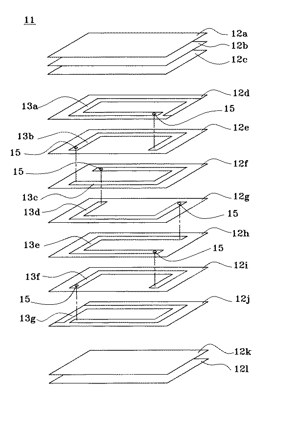
表1から明らかなように、AlをAl2O3に換算して11.5〜60.0重量%、SiをSiO2に換算して4.0〜70.0重量%、BaをBaOに換算して4.0〜40.0重量%、BをB2O3に換算して1.0〜30.0重量%、およびCrをCr2O3に換算して0.3〜3.0重量%含有する、本発明の範囲内の酸化物磁器組成物は、200MPa以上の優れた抗折強度を示す。また、Qは1000以上を示し、はんだ付け性に優れる。 As is apparent from Table 1, Al is converted to Al 2 O 3 in an amount of 11.5 to 60.0% by weight, Si is converted into SiO 2 in an amount of 4.0 to 70.0% by weight, and Ba is converted into BaO. 4.0 to 40.0 wt% in terms of conversion, B to 1.0 to 30.0 wt% in terms of B 2 O 3 , and Cr to 0.3 2 to 3 in terms of Cr 2 O 3 . The oxide porcelain composition within the scope of the present invention containing 0% by weight exhibits an excellent bending strength of 200 MPa or more. Moreover, Q shows 1000 or more and is excellent in solderability.
これに対して、試料1、2に示すように、Al2O3量が11.5重量%未満か、試料30に示すように60.0重量%を超える場合は、抗折強度が200MPa未満と低い。
On the other hand, when the Al 2 O 3 content is less than 11.5% by weight as shown in
Al2O3の含有量によって抗折強度が変化するのは、Al化合物の析出によるものであるが、Al2O3の含有量が11.5重量%未満であると、Al化合物が十分析出しないため、抗折強度は200MPa未満と低い。また、Al2O3の含有量が60.0重量%を超えると焼結性が悪化して磁器焼結体が十分に緻密化しないため、抗折強度は200MPa未満に低下する。 The bending strength varies depending on the Al 2 O 3 content because of precipitation of the Al compound, but if the Al 2 O 3 content is less than 11.5% by weight, the Al compound is sufficiently analyzed. Since it does not come out, the bending strength is as low as less than 200 MPa. On the other hand, if the content of Al 2 O 3 exceeds 60.0% by weight, the sinterability is deteriorated and the ceramic sintered body is not sufficiently densified, so that the bending strength is reduced to less than 200 MPa.
また、試料28、6に示すように、SiO2が4.0重量%未満か、70.0重量%を超えると、焼結性が悪化して焼結体が十分に緻密化しにくくなり、Qが1000未満となる。 Further, as shown in Samples 28 and 6, when SiO 2 is less than 4.0% by weight or more than 70.0% by weight, the sinterability is deteriorated and the sintered body is not sufficiently densified. Is less than 1000.
また、試料22、10に示すように、BaOが4.0重量%未満か、40.0重量%を超えると、焼結性が悪化して焼結体が十分に緻密化しにくくなり、Qが1000未満となる。 Further, as shown in Samples 22 and 10, when BaO is less than 4.0% by weight or exceeds 40.0% by weight, the sinterability deteriorates and the sintered body becomes difficult to be sufficiently densified, and Q is Less than 1000.
また、試料4に示すように、B2O3が1.0重量%未満では、焼結性が悪化して磁器焼結体が十分に緻密化しにくくなり、Qが1000未満となる。一方、試料27に示すように、B2O3が30.0重量%を超えると、非晶質相が増加し、Qが1000未満となる。
Further, as shown in
また、試料15、13に示すように、Cr2O3が0.3重量%未満か、3.0重量%を超えると、はんだ付け性がやや悪くなる。なお、焼成時、電極表面にガラス相が浮き出るとはんだ付け性が悪化するが、Crにはガラス相の流動を防ぐ効果があり、はんだ付け性の悪化を防ぐことができる。
Further, as shown in
出発原料として、実施例1と同じSiO2、BaCO3、Al2O3、B2O3およびCr2O3を準備した。また、いずれも粒径2.0μm以下のCaCO3、Mg(OH)2、ZnOおよびSrCO3を準備した。 As starting materials, the same SiO 2 , BaCO 3 , Al 2 O 3 , B 2 O 3 and Cr 2 O 3 as in Example 1 were prepared. Also, CaCO 3 , Mg (OH) 2 , ZnO and SrCO 3 having a particle size of 2.0 μm or less were prepared.
その後、実施例1と同様にして、表2に示す組成比率の磁器試料を得た。なお、焼成に際して、同一組成の試料について焼成温度を振り、焼成可能温度範囲を求めた。 Thereafter, in the same manner as in Example 1, ceramic samples having the composition ratios shown in Table 2 were obtained. During firing, the firing temperature was varied for samples having the same composition, and the firing possible temperature range was determined.
一般に、セラミック焼成時の焼成収縮率の挙動は、焼成温度の上昇に伴ってある温度までは焼成収縮率が大きくなり、ある温度で最大値をとり、その後は逆に小さくなる傾向を示す。本発明においては、その焼成収縮率が最大値をとる温度を試料の最適焼成温度とし、さらにその収縮率の最大値との差が0.5%以内となる温度範囲を焼成可能温度範囲とし、易焼結性を示すパラメータとした。 Generally, the firing shrinkage behavior during ceramic firing tends to increase as the firing temperature increases up to a certain temperature, takes a maximum value at a certain temperature, and then decreases. In the present invention, the temperature at which the firing shrinkage rate takes the maximum value is the optimum firing temperature of the sample, and the temperature range where the difference from the maximum shrinkage rate is within 0.5% is the firing possible temperature range, The parameter was set to indicate easy sinterability.
以上の結果を表2に示す。なお、表2中、試料番号に◎印を付したものは本発明のより好ましい範囲のものであり、それ以外は本発明の範囲内にあるが、より好ましい範囲外のものである。 The results are shown in Table 2. In Table 2, the sample numbers marked with ◎ are those within the more preferred range of the present invention, and others are within the scope of the present invention, but are outside the more preferred range.
表2から明らかなように、副成分としてCaO、MgO、ZnOおよびSrOから選ばれる少なくとも1種を合計量で3重量部以下含有させることにより、焼成可能温度範囲が広くなり、焼結が容易となる。これに対して、試料35、41に示すように、CaO、MgO、ZnOおよびSrOから選ばれる少なくとも1種を合計量で3重量部を超えて含有するものは、焼成温度が1000℃前後に上昇し、焼成可能温度範囲の幅も上記酸化物が無添加の場合(試料31)と比べて大差なくなる。 As is apparent from Table 2, the inclusion of at least one selected from CaO, MgO, ZnO and SrO as subcomponents in a total amount of 3 parts by weight or less widens the sinterable temperature range and facilitates sintering. Become. On the other hand, as shown in samples 35 and 41, those containing at least one selected from CaO, MgO, ZnO and SrO in a total amount exceeding 3 parts by weight increase the firing temperature to around 1000 ° C. And the width of the sinterable temperature range is not much different from that in the case where the oxide is not added (sample 31).
出発原料として、実施例1と同じ原料を準備した。その後、実施例1と同様にして、表1の試料8に示す組成比率の磁器組成物が得られるように調合し、スラリーを調整し、グリーンシートを得た。 The same raw material as in Example 1 was prepared as a starting raw material. Thereafter, in the same manner as in Example 1, the mixture was prepared so that a ceramic composition having the composition ratio shown in Sample 8 of Table 1 was obtained, the slurry was adjusted, and a green sheet was obtained.
その後、このグリーンシートを所定の寸法にカットし、カットした複数のグリーンシートの表面にスクリーン印刷法によりCuを主成分とする導体パターンを形成した。この導体パターンを形成した複数のグリーンシートにパンチャーを用いてビアホールを形成して、Cuを主成分とする導体を充填した。そして、各グリーンシート表面の導体パターンを互いに電気的に接続できるようにして積み重ね、圧着した。このグリーンシート圧着体を窒素−水素の非酸化性雰囲気中、980℃で焼成した。 Thereafter, the green sheet was cut into a predetermined dimension, and a conductor pattern mainly composed of Cu was formed on the surfaces of the cut green sheets by a screen printing method. Via holes were formed in the plurality of green sheets on which the conductor pattern was formed using a puncher, and a conductor mainly composed of Cu was filled. The conductor patterns on the surface of each green sheet were stacked and crimped so that they could be electrically connected to each other. This green sheet pressure-bonded body was fired at 980 ° C. in a non-oxidizing atmosphere of nitrogen-hydrogen.
これにより、図1に示すような、セラミック層1、ビアホール2で電気的に接続された内部導体3を備えるセラミック多層基板を得た。
As a result, a ceramic multilayer substrate including an
次に、得られたセラミック多層基板について、実施例1と同様にして抗折強度を測定したところ、200MPa以上の優れた抗折強度が得られた。 Next, when the bending strength of the obtained ceramic multilayer substrate was measured in the same manner as in Example 1, an excellent bending strength of 200 MPa or more was obtained.
図2は、本発明のセラミック電子部品の一実施形態である積層インダクタ11の斜視図である。また図3は、積層インダクタ11の構成を示す分解斜視図である。
FIG. 2 is a perspective view of a
積層インダクタ11は、複数のセラミック層が積層されてなるセラミック体12と、セラミック体12の内部に形成された内部導体13a〜13gと、セラミック体12の表面に、内部導体13a〜13gと導通するように形成された、外部電極14a、14bとによって構成されている。
The
セラミック体12は、本発明の磁器組成物よりなる。内部導体13a〜13gは、各々が電気的に直列に接続され、螺旋状のコイルを形成している。外部電極14aは、内部導体13a〜13gによって形成されたコイルの一端と接続するように、外部電極14bは、そのコイルの他端と接続するように、セラミック体12の表面に形成されている。
The
以下、図3に基づき、積層インダクタ11の製造方法を説明する。出発原料として、実施例1と同じ原料を準備した。その後、実施例1と同様にして、表1の試料8に示す組成比率の磁器組成物が得られるように調合し、スラリーを調整し、グリーンシート12a〜12lを得た。
Hereinafter, a method of manufacturing the
グリーンシート12d〜12iには、その厚み方向に貫通孔を設け、その貫通孔にCuを主成分とする導電性ペーストを充填することで、ビアホール15を形成した。さらに、グリーンシート12d〜12jの表面には、Cuを主成分とする内部導体13a〜13gをスクリーン印刷によって形成した。内部導体13a〜13gは、ビアホール15を介して電気接続され、全体として螺旋状のコイルを形成する。
The
次に、グリーンシート12a〜12lを積層し、厚み方向に加圧して、積層体を得た。Cuを主成分とするペーストをこの積層体の両端部に塗布し、窒素−水素の非酸化性雰囲気中、980℃で焼成した。これにより、セラミック体12を得た。セラミック体12の両端部には、外部電極14a、14bが形成された。
Next,
得られたセラミック体12を、メッキ液に浸漬し、外部電極14a、14bの表面に、第1のメッキ皮膜としてニッケル電解メッキ膜(図示せず)、第2のメッキ皮膜としてスズメッキ膜(図示せず)を形成し、積層インダクタ11を得た。
The obtained
なお、本実施例においてセラミック体12はシート積層で形成されているが、印刷や転写などの工法によって形成されてもよく、内部導体13a〜13gは、転写などの工法によって形成されてもよい。また、グリーンシート12d〜12iの貫通孔への導電性ペーストの充填と、内部導体13a〜13gの形成とは、同時に行われてもよい。外部電極14a、14bについては、焼成後に焼付などの方法により形成してもよい。
In this embodiment, the
また、本発明のセラミック電子部品は、本実施例のように積層インダクタに限らず、射出成形などによって形成されたコイル型電子部品であってもよく、またコンデンサやLC複合部品などの電子部品であってもよい。 Further, the ceramic electronic component of the present invention is not limited to the multilayer inductor as in the present embodiment, but may be a coil-type electronic component formed by injection molding or the like, or an electronic component such as a capacitor or an LC composite component. There may be.
本実施例における積層インダクタ11によれば、本発明の磁器組成物を用いているため、特性や信頼性の低下が抑えられ、製造歩留を向上させることができる。また、内部導体13a〜13gおよび外部電極14a、14bとして、いずれもCuを主成分とするペーストを用いているため、焼成時に内部導体13a〜13gや外部電極14a、14bの融解や揮発による焼失を防止することができる。さらに、内部導体13a〜13gと外部電極14a、14bとの界面に十分な接合性を持たせることができる。
According to the
1 セラミック層
2 ビアホール
3 内部導体
4 外部導体
11 積層インダクタ
12 セラミック体
13 内部導体
14 外部電極
DESCRIPTION OF SYMBOLS 1
Claims (5)
Priority Applications (1)
| Application Number | Priority Date | Filing Date | Title |
|---|---|---|---|
| JP2003324791A JP4419487B2 (en) | 2002-10-09 | 2003-09-17 | Oxide porcelain composition, ceramic multilayer substrate and ceramic electronic component |
Applications Claiming Priority (2)
| Application Number | Priority Date | Filing Date | Title |
|---|---|---|---|
| JP2002296705 | 2002-10-09 | ||
| JP2003324791A JP4419487B2 (en) | 2002-10-09 | 2003-09-17 | Oxide porcelain composition, ceramic multilayer substrate and ceramic electronic component |
Publications (2)
| Publication Number | Publication Date |
|---|---|
| JP2004149405A true JP2004149405A (en) | 2004-05-27 |
| JP4419487B2 JP4419487B2 (en) | 2010-02-24 |
Family
ID=32473541
Family Applications (1)
| Application Number | Title | Priority Date | Filing Date |
|---|---|---|---|
| JP2003324791A Expired - Lifetime JP4419487B2 (en) | 2002-10-09 | 2003-09-17 | Oxide porcelain composition, ceramic multilayer substrate and ceramic electronic component |
Country Status (1)
| Country | Link |
|---|---|
| JP (1) | JP4419487B2 (en) |
Cited By (3)
| Publication number | Priority date | Publication date | Assignee | Title |
|---|---|---|---|---|
| WO2008126486A1 (en) * | 2007-04-09 | 2008-10-23 | Murata Manufacturing Co., Ltd. | Dielectric ceramic composition, ceramic substrate, and method for producing the same |
| WO2010092969A1 (en) * | 2009-02-16 | 2010-08-19 | 株式会社村田製作所 | Low temperature cofired ceramic material and ceramic substrate |
| EP2386528A1 (en) * | 2009-01-07 | 2011-11-16 | Murata Manufacturing Co., Ltd. | Ceramic material for low-temperature sintering, and ceramic substrate |
-
2003
- 2003-09-17 JP JP2003324791A patent/JP4419487B2/en not_active Expired - Lifetime
Cited By (8)
| Publication number | Priority date | Publication date | Assignee | Title |
|---|---|---|---|---|
| WO2008126486A1 (en) * | 2007-04-09 | 2008-10-23 | Murata Manufacturing Co., Ltd. | Dielectric ceramic composition, ceramic substrate, and method for producing the same |
| JPWO2008126486A1 (en) * | 2007-04-09 | 2010-07-22 | 株式会社村田製作所 | Ceramic substrate and manufacturing method thereof |
| US7790271B2 (en) | 2007-04-09 | 2010-09-07 | Murata Manufacturing Co., Ltd. | Dielectric ceramic composition, ceramic substrate, and method for producing the same |
| JP5104761B2 (en) * | 2007-04-09 | 2012-12-19 | 株式会社村田製作所 | Ceramic substrate and manufacturing method thereof |
| EP2386528A1 (en) * | 2009-01-07 | 2011-11-16 | Murata Manufacturing Co., Ltd. | Ceramic material for low-temperature sintering, and ceramic substrate |
| EP2386528A4 (en) * | 2009-01-07 | 2014-01-01 | Murata Manufacturing Co | Ceramic material for low-temperature sintering, and ceramic substrate |
| WO2010092969A1 (en) * | 2009-02-16 | 2010-08-19 | 株式会社村田製作所 | Low temperature cofired ceramic material and ceramic substrate |
| JP5533674B2 (en) * | 2009-02-16 | 2014-06-25 | 株式会社村田製作所 | Low temperature sintered ceramic material and ceramic substrate |
Also Published As
| Publication number | Publication date |
|---|---|
| JP4419487B2 (en) | 2010-02-24 |
Similar Documents
| Publication | Publication Date | Title |
|---|---|---|
| US7211533B2 (en) | Oxide porcelain composition, ceramic multilayer substrate, and ceramic electronic component | |
| KR100814674B1 (en) | Dielectric porcelain composition and method for production thereof | |
| JP4839913B2 (en) | Electronic component, dielectric ceramic composition and method for producing the same | |
| JP2007331956A (en) | Electronic component, dielectric ceramic composition and method for producing the same | |
| JP5435176B2 (en) | Composite multilayer ceramic electronic components | |
| WO2010092970A1 (en) | Sintered body of low temperature cofired ceramic and multilayer ceramic substrate | |
| JP2007331958A (en) | Electronic component, dielectric ceramic composition and method for producing the same | |
| JP5761341B2 (en) | Glass ceramic composition | |
| JP2009088089A (en) | Ceramic multilayer substrate | |
| JP6458863B2 (en) | Low temperature sintered ceramic materials, ceramic sintered bodies and ceramic electronic components | |
| JP2007331957A (en) | Dielectric ceramic composition, electronic component and its production method | |
| JP2009007209A (en) | Dielectric porcelain and laminated ceramic capacitor using it | |
| JP4696891B2 (en) | Electronic component, dielectric ceramic composition and method for producing the same | |
| JP2012156171A (en) | Multilayer ceramic capacitor and manufacturing method of the same | |
| JP4419487B2 (en) | Oxide porcelain composition, ceramic multilayer substrate and ceramic electronic component | |
| JP4547945B2 (en) | Electronic component, dielectric ceramic composition and method for producing the same | |
| JP2007230819A (en) | Dielectric ceramic composition, electronic component, and method for producing the same | |
| JP2006202857A (en) | Laminated ceramic electronic component and its manufacturing method | |
| JP3981270B2 (en) | Conductor pattern incorporated in multilayer substrate, multilayer substrate incorporating conductor pattern, and method of manufacturing multilayer substrate | |
| KR20170012069A (en) | Composite electric device | |
| JP4691977B2 (en) | Method for manufacturing dielectric composition | |
| JP4802490B2 (en) | Electronic component, dielectric ceramic composition and method for producing the same | |
| JP4691978B2 (en) | Method for manufacturing dielectric composition | |
| JP4449344B2 (en) | Oxide porcelain composition and ceramic multilayer substrate | |
| JP3645046B2 (en) | Non-magnetic ceramic and ceramic laminated parts |
Legal Events
| Date | Code | Title | Description |
|---|---|---|---|
| A621 | Written request for application examination |
Free format text: JAPANESE INTERMEDIATE CODE: A621 Effective date: 20050627 |
|
| A977 | Report on retrieval |
Free format text: JAPANESE INTERMEDIATE CODE: A971007 Effective date: 20080616 |
|
| A131 | Notification of reasons for refusal |
Free format text: JAPANESE INTERMEDIATE CODE: A131 Effective date: 20080708 |
|
| A521 | Request for written amendment filed |
Free format text: JAPANESE INTERMEDIATE CODE: A523 Effective date: 20080905 |
|
| A131 | Notification of reasons for refusal |
Free format text: JAPANESE INTERMEDIATE CODE: A131 Effective date: 20090210 |
|
| A521 | Request for written amendment filed |
Free format text: JAPANESE INTERMEDIATE CODE: A523 Effective date: 20090410 |
|
| TRDD | Decision of grant or rejection written | ||
| A01 | Written decision to grant a patent or to grant a registration (utility model) |
Free format text: JAPANESE INTERMEDIATE CODE: A01 Effective date: 20091110 |
|
| A01 | Written decision to grant a patent or to grant a registration (utility model) |
Free format text: JAPANESE INTERMEDIATE CODE: A01 |
|
| A61 | First payment of annual fees (during grant procedure) |
Free format text: JAPANESE INTERMEDIATE CODE: A61 Effective date: 20091123 |
|
| FPAY | Renewal fee payment (event date is renewal date of database) |
Free format text: PAYMENT UNTIL: 20121211 Year of fee payment: 3 |
|
| R150 | Certificate of patent or registration of utility model |
Ref document number: 4419487 Country of ref document: JP Free format text: JAPANESE INTERMEDIATE CODE: R150 Free format text: JAPANESE INTERMEDIATE CODE: R150 |
|
| FPAY | Renewal fee payment (event date is renewal date of database) |
Free format text: PAYMENT UNTIL: 20131211 Year of fee payment: 4 |
|
| EXPY | Cancellation because of completion of term |